US10636975B2 - Organic semiconductor element, compound, organic semiconductor composition, and method of manufacturing organic semiconductor film - Google Patents
Organic semiconductor element, compound, organic semiconductor composition, and method of manufacturing organic semiconductor film Download PDFInfo
- Publication number
- US10636975B2 US10636975B2 US15/857,746 US201715857746A US10636975B2 US 10636975 B2 US10636975 B2 US 10636975B2 US 201715857746 A US201715857746 A US 201715857746A US 10636975 B2 US10636975 B2 US 10636975B2
- Authority
- US
- United States
- Prior art keywords
- independently represent
- group
- atom
- formula
- monovalent
- Prior art date
- Legal status (The legal status is an assumption and is not a legal conclusion. Google has not performed a legal analysis and makes no representation as to the accuracy of the status listed.)
- Active, expires
Links
- 239000004065 semiconductor Substances 0.000 title claims abstract description 183
- 150000001875 compounds Chemical class 0.000 title claims abstract description 115
- 239000000203 mixture Substances 0.000 title claims abstract description 67
- 238000004519 manufacturing process Methods 0.000 title claims abstract description 16
- 125000000217 alkyl group Chemical group 0.000 claims abstract description 100
- 125000004432 carbon atom Chemical group C* 0.000 claims abstract description 77
- 125000006615 aromatic heterocyclic group Chemical group 0.000 claims abstract description 48
- 125000002029 aromatic hydrocarbon group Chemical group 0.000 claims abstract description 38
- 125000002947 alkylene group Chemical group 0.000 claims abstract description 18
- 125000004435 hydrogen atom Chemical group [H]* 0.000 claims description 72
- 125000001424 substituent group Chemical group 0.000 claims description 62
- 125000004434 sulfur atom Chemical group 0.000 claims description 50
- 125000004430 oxygen atom Chemical group O* 0.000 claims description 46
- 229910052711 selenium Chemical group 0.000 claims description 42
- 239000002904 solvent Substances 0.000 claims description 38
- 239000000758 substrate Substances 0.000 claims description 38
- 125000004433 nitrogen atom Chemical group N* 0.000 claims description 36
- 125000004429 atom Chemical group 0.000 claims description 31
- 125000000962 organic group Chemical group 0.000 claims description 28
- 125000005843 halogen group Chemical group 0.000 claims description 26
- 239000011248 coating agent Substances 0.000 claims description 25
- 238000000576 coating method Methods 0.000 claims description 25
- 125000004450 alkenylene group Chemical group 0.000 claims description 17
- 125000004419 alkynylene group Chemical group 0.000 claims description 17
- 229910052757 nitrogen Inorganic materials 0.000 claims description 6
- 125000002915 carbonyl group Chemical group [*:2]C([*:1])=O 0.000 claims description 5
- 125000002813 thiocarbonyl group Chemical group *C(*)=S 0.000 claims description 5
- 229910052760 oxygen Inorganic materials 0.000 claims 11
- 229910052717 sulfur Inorganic materials 0.000 claims 11
- 239000010408 film Substances 0.000 abstract description 90
- 239000010409 thin film Substances 0.000 abstract description 36
- 238000003860 storage Methods 0.000 abstract description 10
- 230000007774 longterm Effects 0.000 abstract description 7
- 238000000034 method Methods 0.000 description 65
- 229920000642 polymer Polymers 0.000 description 64
- 230000000052 comparative effect Effects 0.000 description 53
- 239000010410 layer Substances 0.000 description 52
- 239000011230 binding agent Substances 0.000 description 39
- VLKZOEOYAKHREP-UHFFFAOYSA-N n-Hexane Chemical compound CCCCCC VLKZOEOYAKHREP-UHFFFAOYSA-N 0.000 description 36
- 0 CCCCC(C)(CC)c1cc(C(N(*)C(c2c(cc3C(N4*)=O)-c5ccc(-c6cc(C(C)(*)c7cc(-c8c(*9*)cc(-c%10ccc(C(C)(CCCC)C(CC)CC)[s]%10)[s]8)c9cc7-7)c-7[s]6)[s]5)=O)=O)c2c3c1C4=O Chemical compound CCCCC(C)(CC)c1cc(C(N(*)C(c2c(cc3C(N4*)=O)-c5ccc(-c6cc(C(C)(*)c7cc(-c8c(*9*)cc(-c%10ccc(C(C)(CCCC)C(CC)CC)[s]%10)[s]8)c9cc7-7)c-7[s]6)[s]5)=O)=O)c2c3c1C4=O 0.000 description 27
- XEKOWRVHYACXOJ-UHFFFAOYSA-N Ethyl acetate Chemical compound CCOC(C)=O XEKOWRVHYACXOJ-UHFFFAOYSA-N 0.000 description 27
- 230000015572 biosynthetic process Effects 0.000 description 27
- 238000003786 synthesis reaction Methods 0.000 description 27
- 230000002123 temporal effect Effects 0.000 description 25
- 239000000243 solution Substances 0.000 description 19
- OKKJLVBELUTLKV-UHFFFAOYSA-N Methanol Chemical compound OC OKKJLVBELUTLKV-UHFFFAOYSA-N 0.000 description 18
- 239000000463 material Substances 0.000 description 18
- 238000006243 chemical reaction Methods 0.000 description 17
- 125000001153 fluoro group Chemical group F* 0.000 description 17
- WYURNTSHIVDZCO-UHFFFAOYSA-N Tetrahydrofuran Chemical compound C1CCOC1 WYURNTSHIVDZCO-UHFFFAOYSA-N 0.000 description 16
- VYPSYNLAJGMNEJ-UHFFFAOYSA-N Silicium dioxide Chemical compound O=[Si]=O VYPSYNLAJGMNEJ-UHFFFAOYSA-N 0.000 description 14
- -1 poly(α-methylstyrene) Polymers 0.000 description 13
- 238000007789 sealing Methods 0.000 description 13
- RFFLAFLAYFXFSW-UHFFFAOYSA-N 1,2-dichlorobenzene Chemical compound ClC1=CC=CC=C1Cl RFFLAFLAYFXFSW-UHFFFAOYSA-N 0.000 description 12
- 125000001309 chloro group Chemical group Cl* 0.000 description 11
- 239000012043 crude product Substances 0.000 description 11
- 238000011282 treatment Methods 0.000 description 11
- 238000005227 gel permeation chromatography Methods 0.000 description 10
- 238000007639 printing Methods 0.000 description 10
- PBKONEOXTCPAFI-UHFFFAOYSA-N 1,2,4-trichlorobenzene Chemical compound ClC1=CC=C(Cl)C(Cl)=C1 PBKONEOXTCPAFI-UHFFFAOYSA-N 0.000 description 9
- YXFVVABEGXRONW-UHFFFAOYSA-N Toluene Chemical compound CC1=CC=CC=C1 YXFVVABEGXRONW-UHFFFAOYSA-N 0.000 description 9
- 229940125898 compound 5 Drugs 0.000 description 9
- 239000012299 nitrogen atmosphere Substances 0.000 description 9
- CXWXQJXEFPUFDZ-UHFFFAOYSA-N tetralin Chemical compound C1=CC=C2CCCCC2=C1 CXWXQJXEFPUFDZ-UHFFFAOYSA-N 0.000 description 9
- YMWUJEATGCHHMB-UHFFFAOYSA-N Dichloromethane Chemical compound ClCCl YMWUJEATGCHHMB-UHFFFAOYSA-N 0.000 description 8
- 239000004793 Polystyrene Substances 0.000 description 8
- MVPPADPHJFYWMZ-UHFFFAOYSA-N chlorobenzene Chemical compound ClC1=CC=CC=C1 MVPPADPHJFYWMZ-UHFFFAOYSA-N 0.000 description 8
- 229920002223 polystyrene Polymers 0.000 description 8
- 125000001246 bromo group Chemical group Br* 0.000 description 7
- 238000001914 filtration Methods 0.000 description 7
- 239000011521 glass Substances 0.000 description 7
- 125000002346 iodo group Chemical group I* 0.000 description 7
- 238000003756 stirring Methods 0.000 description 7
- CHLICZRVGGXEOD-UHFFFAOYSA-N 1-Methoxy-4-methylbenzene Chemical compound COC1=CC=C(C)C=C1 CHLICZRVGGXEOD-UHFFFAOYSA-N 0.000 description 6
- XHLHPRDBBAGVEG-UHFFFAOYSA-N 1-tetralone Chemical compound C1=CC=C2C(=O)CCCC2=C1 XHLHPRDBBAGVEG-UHFFFAOYSA-N 0.000 description 6
- HBEDSQVIWPRPAY-UHFFFAOYSA-N 2,3-dihydrobenzofuran Chemical compound C1=CC=C2OCCC2=C1 HBEDSQVIWPRPAY-UHFFFAOYSA-N 0.000 description 6
- ZWEHNKRNPOVVGH-UHFFFAOYSA-N 2-Butanone Chemical compound CCC(C)=O ZWEHNKRNPOVVGH-UHFFFAOYSA-N 0.000 description 6
- CSCPPACGZOOCGX-UHFFFAOYSA-N Acetone Chemical compound CC(C)=O CSCPPACGZOOCGX-UHFFFAOYSA-N 0.000 description 6
- KWOLFJPFCHCOCG-UHFFFAOYSA-N Acetophenone Chemical compound CC(=O)C1=CC=CC=C1 KWOLFJPFCHCOCG-UHFFFAOYSA-N 0.000 description 6
- OKTJSMMVPCPJKN-UHFFFAOYSA-N Carbon Chemical compound [C] OKTJSMMVPCPJKN-UHFFFAOYSA-N 0.000 description 6
- CSNNHWWHGAXBCP-UHFFFAOYSA-L Magnesium sulfate Chemical compound [Mg+2].[O-][S+2]([O-])([O-])[O-] CSNNHWWHGAXBCP-UHFFFAOYSA-L 0.000 description 6
- ZMXDDKWLCZADIW-UHFFFAOYSA-N N,N-Dimethylformamide Chemical compound CN(C)C=O ZMXDDKWLCZADIW-UHFFFAOYSA-N 0.000 description 6
- RDOXTESZEPMUJZ-UHFFFAOYSA-N anisole Chemical compound COC1=CC=CC=C1 RDOXTESZEPMUJZ-UHFFFAOYSA-N 0.000 description 6
- 229910052799 carbon Inorganic materials 0.000 description 6
- 239000000706 filtrate Substances 0.000 description 6
- 125000001997 phenyl group Chemical group [H]C1=C([H])C([H])=C(*)C([H])=C1[H] 0.000 description 6
- 238000010898 silica gel chromatography Methods 0.000 description 6
- 238000004528 spin coating Methods 0.000 description 6
- YLQBMQCUIZJEEH-UHFFFAOYSA-N tetrahydrofuran Natural products C=1C=COC=1 YLQBMQCUIZJEEH-UHFFFAOYSA-N 0.000 description 6
- BOWLIEKXXONYAR-UHFFFAOYSA-N CC1=CC=C(CC2=CC=C(C)C2)C1 Chemical compound CC1=CC=C(CC2=CC=C(C)C2)C1 BOWLIEKXXONYAR-UHFFFAOYSA-N 0.000 description 5
- HEDRZPFGACZZDS-UHFFFAOYSA-N Chloroform Chemical compound ClC(Cl)Cl HEDRZPFGACZZDS-UHFFFAOYSA-N 0.000 description 5
- 125000003545 alkoxy group Chemical group 0.000 description 5
- 239000003795 chemical substances by application Substances 0.000 description 5
- 238000001035 drying Methods 0.000 description 5
- 238000011156 evaluation Methods 0.000 description 5
- 238000007641 inkjet printing Methods 0.000 description 5
- 229910052809 inorganic oxide Inorganic materials 0.000 description 5
- 239000012044 organic layer Substances 0.000 description 5
- 229920000620 organic polymer Polymers 0.000 description 5
- 238000007650 screen-printing Methods 0.000 description 5
- 239000007787 solid Substances 0.000 description 5
- QPFMBZIOSGYJDE-UHFFFAOYSA-N 1,1,2,2-tetrachloroethane Chemical compound ClC(Cl)C(Cl)Cl QPFMBZIOSGYJDE-UHFFFAOYSA-N 0.000 description 4
- CWLKTJOTWITYSI-UHFFFAOYSA-N 1-fluoronaphthalene Chemical compound C1=CC=C2C(F)=CC=CC2=C1 CWLKTJOTWITYSI-UHFFFAOYSA-N 0.000 description 4
- MZQSGHAFQGSNFW-UHFFFAOYSA-N CC.CC.CC.CC.CC1=CC2=C(C=C(C)C3=NCN=C32)C2=NCN=C12.CC1=CC=C(C)C2=NCN=C12.Cc1c2ncnc2c(C)c2ncnc12.[Y]=C1CC(=[Y])C2=C3C1=CC=C1C(=[Y])CC(=[Y])C(=C13)/C=C\2.[Y]=C1CC(=[Y])C2=C3C1=CC=C1C4=CC=C5C(=[Y])CC(=[Y])C6=C5C4=C(/C=C\6)C(=C13)/C=C\2 Chemical compound CC.CC.CC.CC.CC1=CC2=C(C=C(C)C3=NCN=C32)C2=NCN=C12.CC1=CC=C(C)C2=NCN=C12.Cc1c2ncnc2c(C)c2ncnc12.[Y]=C1CC(=[Y])C2=C3C1=CC=C1C(=[Y])CC(=[Y])C(=C13)/C=C\2.[Y]=C1CC(=[Y])C2=C3C1=CC=C1C4=CC=C5C(=[Y])CC(=[Y])C6=C5C4=C(/C=C\6)C(=C13)/C=C\2 MZQSGHAFQGSNFW-UHFFFAOYSA-N 0.000 description 4
- VEXZGXHMUGYJMC-UHFFFAOYSA-N Hydrochloric acid Chemical compound Cl VEXZGXHMUGYJMC-UHFFFAOYSA-N 0.000 description 4
- PWATWSYOIIXYMA-UHFFFAOYSA-N Pentylbenzene Chemical compound CCCCCC1=CC=CC=C1 PWATWSYOIIXYMA-UHFFFAOYSA-N 0.000 description 4
- BQCADISMDOOEFD-UHFFFAOYSA-N Silver Chemical compound [Ag] BQCADISMDOOEFD-UHFFFAOYSA-N 0.000 description 4
- 239000000654 additive Substances 0.000 description 4
- 125000003342 alkenyl group Chemical group 0.000 description 4
- 125000000304 alkynyl group Chemical group 0.000 description 4
- 125000003118 aryl group Chemical group 0.000 description 4
- 238000007611 bar coating method Methods 0.000 description 4
- 238000009835 boiling Methods 0.000 description 4
- 229940125904 compound 1 Drugs 0.000 description 4
- 238000007606 doctor blade method Methods 0.000 description 4
- 125000003983 fluorenyl group Chemical group C1(=CC=CC=2C3=CC=CC=C3CC12)* 0.000 description 4
- 125000005842 heteroatom Chemical group 0.000 description 4
- 125000000623 heterocyclic group Chemical group 0.000 description 4
- 125000004957 naphthylene group Chemical group 0.000 description 4
- 239000003960 organic solvent Substances 0.000 description 4
- 229910052709 silver Inorganic materials 0.000 description 4
- 239000004332 silver Substances 0.000 description 4
- 230000002194 synthesizing effect Effects 0.000 description 4
- 238000010345 tape casting Methods 0.000 description 4
- OSIGJGFTADMDOB-UHFFFAOYSA-N 1-Methoxy-3-methylbenzene Chemical compound COC1=CC=CC(C)=C1 OSIGJGFTADMDOB-UHFFFAOYSA-N 0.000 description 3
- KBVDUUXRXJTAJC-UHFFFAOYSA-N 2,5-dibromothiophene Chemical compound BrC1=CC=C(Br)S1 KBVDUUXRXJTAJC-UHFFFAOYSA-N 0.000 description 3
- DTFKRVXLBCAIOZ-UHFFFAOYSA-N 2-methylanisole Chemical compound COC1=CC=CC=C1C DTFKRVXLBCAIOZ-UHFFFAOYSA-N 0.000 description 3
- QUBJDMPBDURTJT-UHFFFAOYSA-N 3-chlorothiophene Chemical compound ClC=1C=CSC=1 QUBJDMPBDURTJT-UHFFFAOYSA-N 0.000 description 3
- 229940077398 4-methyl anisole Drugs 0.000 description 3
- WEVYAHXRMPXWCK-UHFFFAOYSA-N Acetonitrile Chemical compound CC#N WEVYAHXRMPXWCK-UHFFFAOYSA-N 0.000 description 3
- UHOVQNZJYSORNB-UHFFFAOYSA-N Benzene Chemical group C1=CC=CC=C1 UHOVQNZJYSORNB-UHFFFAOYSA-N 0.000 description 3
- YNQLUTRBYVCPMQ-UHFFFAOYSA-N Ethylbenzene Chemical compound CCC1=CC=CC=C1 YNQLUTRBYVCPMQ-UHFFFAOYSA-N 0.000 description 3
- LYCAIKOWRPUZTN-UHFFFAOYSA-N Ethylene glycol Chemical compound OCCO LYCAIKOWRPUZTN-UHFFFAOYSA-N 0.000 description 3
- CTQNGGLPUBDAKN-UHFFFAOYSA-N O-Xylene Chemical compound CC1=CC=CC=C1C CTQNGGLPUBDAKN-UHFFFAOYSA-N 0.000 description 3
- FAPWRFPIFSIZLT-UHFFFAOYSA-M Sodium chloride Chemical class [Na+].[Cl-] FAPWRFPIFSIZLT-UHFFFAOYSA-M 0.000 description 3
- YTPLMLYBLZKORZ-UHFFFAOYSA-N Thiophene Chemical group C=1C=CSC=1 YTPLMLYBLZKORZ-UHFFFAOYSA-N 0.000 description 3
- 150000004945 aromatic hydrocarbons Chemical class 0.000 description 3
- JFDZBHWFFUWGJE-UHFFFAOYSA-N benzonitrile Chemical compound N#CC1=CC=CC=C1 JFDZBHWFFUWGJE-UHFFFAOYSA-N 0.000 description 3
- YFNONBGXNFCTMM-UHFFFAOYSA-N butoxybenzene Chemical compound CCCCOC1=CC=CC=C1 YFNONBGXNFCTMM-UHFFFAOYSA-N 0.000 description 3
- FFSAXUULYPJSKH-UHFFFAOYSA-N butyrophenone Chemical compound CCCC(=O)C1=CC=CC=C1 FFSAXUULYPJSKH-UHFFFAOYSA-N 0.000 description 3
- 239000011575 calcium Substances 0.000 description 3
- VZWXIQHBIQLMPN-UHFFFAOYSA-N chromane Chemical compound C1=CC=C2CCCOC2=C1 VZWXIQHBIQLMPN-UHFFFAOYSA-N 0.000 description 3
- 229940125782 compound 2 Drugs 0.000 description 3
- 238000004132 cross linking Methods 0.000 description 3
- 230000000694 effects Effects 0.000 description 3
- 230000005669 field effect Effects 0.000 description 3
- 239000010931 gold Substances 0.000 description 3
- 238000010438 heat treatment Methods 0.000 description 3
- RAXXELZNTBOGNW-UHFFFAOYSA-N imidazole Natural products C1=CNC=N1 RAXXELZNTBOGNW-UHFFFAOYSA-N 0.000 description 3
- HEBMCVBCEDMUOF-UHFFFAOYSA-N isochromane Chemical compound C1=CC=C2COCCC2=C1 HEBMCVBCEDMUOF-UHFFFAOYSA-N 0.000 description 3
- 229910052943 magnesium sulfate Inorganic materials 0.000 description 3
- 235000019341 magnesium sulphate Nutrition 0.000 description 3
- UZKWTJUDCOPSNM-UHFFFAOYSA-N methoxybenzene Substances CCCCOC=C UZKWTJUDCOPSNM-UHFFFAOYSA-N 0.000 description 3
- 239000000178 monomer Substances 0.000 description 3
- DLRJIFUOBPOJNS-UHFFFAOYSA-N phenetole Chemical compound CCOC1=CC=CC=C1 DLRJIFUOBPOJNS-UHFFFAOYSA-N 0.000 description 3
- SFLGSKRGOWRGBR-UHFFFAOYSA-N phthalane Chemical compound C1=CC=C2COCC2=C1 SFLGSKRGOWRGBR-UHFFFAOYSA-N 0.000 description 3
- 229920003023 plastic Polymers 0.000 description 3
- 239000004033 plastic Substances 0.000 description 3
- 229920002492 poly(sulfone) Polymers 0.000 description 3
- 229920001721 polyimide Polymers 0.000 description 3
- BWHMMNNQKKPAPP-UHFFFAOYSA-L potassium carbonate Substances [K+].[K+].[O-]C([O-])=O BWHMMNNQKKPAPP-UHFFFAOYSA-L 0.000 description 3
- 239000002243 precursor Substances 0.000 description 3
- KRIOVPPHQSLHCZ-UHFFFAOYSA-N propiophenone Chemical compound CCC(=O)C1=CC=CC=C1 KRIOVPPHQSLHCZ-UHFFFAOYSA-N 0.000 description 3
- DSNYFFJTZPIKFZ-UHFFFAOYSA-N propoxybenzene Chemical compound CCCOC1=CC=CC=C1 DSNYFFJTZPIKFZ-UHFFFAOYSA-N 0.000 description 3
- 238000000746 purification Methods 0.000 description 3
- 239000000741 silica gel Substances 0.000 description 3
- 229910002027 silica gel Inorganic materials 0.000 description 3
- 238000006467 substitution reaction Methods 0.000 description 3
- DOIRPCDOGSNNCS-UHFFFAOYSA-N trimethyl-[5-(5-trimethylstannylthiophen-2-yl)thiophen-2-yl]stannane Chemical compound S1C([Sn](C)(C)C)=CC=C1C1=CC=C([Sn](C)(C)C)S1 DOIRPCDOGSNNCS-UHFFFAOYSA-N 0.000 description 3
- 239000008096 xylene Substances 0.000 description 3
- CBMXCNPQDUJNHT-UHFFFAOYSA-N 1,6-dimethylnaphthalene Chemical compound CC1=CC=CC2=CC(C)=CC=C21 CBMXCNPQDUJNHT-UHFFFAOYSA-N 0.000 description 2
- HDNRAPAFJLXKBV-UHFFFAOYSA-N 1-ethyl-4-methoxybenzene Chemical compound CCC1=CC=C(OC)C=C1 HDNRAPAFJLXKBV-UHFFFAOYSA-N 0.000 description 2
- QPUYECUOLPXSFR-UHFFFAOYSA-N 1-methylnaphthalene Chemical compound C1=CC=C2C(C)=CC=CC2=C1 QPUYECUOLPXSFR-UHFFFAOYSA-N 0.000 description 2
- RKMGAJGJIURJSJ-UHFFFAOYSA-N 2,2,6,6-tetramethylpiperidine Chemical compound CC1(C)CCCC(C)(C)N1 RKMGAJGJIURJSJ-UHFFFAOYSA-N 0.000 description 2
- KCKZIWSINLBROE-UHFFFAOYSA-N 3,4-dihydro-1h-naphthalen-2-one Chemical compound C1=CC=C2CC(=O)CCC2=C1 KCKZIWSINLBROE-UHFFFAOYSA-N 0.000 description 2
- YEJRWHAVMIAJKC-UHFFFAOYSA-N 4-Butyrolactone Chemical compound O=C1CCCO1 YEJRWHAVMIAJKC-UHFFFAOYSA-N 0.000 description 2
- ZCYVEMRRCGMTRW-UHFFFAOYSA-N 7553-56-2 Chemical compound [I] ZCYVEMRRCGMTRW-UHFFFAOYSA-N 0.000 description 2
- XSQSDBVMLJNZKU-UHFFFAOYSA-N 9-(bromomethyl)nonadecane Chemical compound CCCCCCCCCCC(CBr)CCCCCCCC XSQSDBVMLJNZKU-UHFFFAOYSA-N 0.000 description 2
- IJGRMHOSHXDMSA-UHFFFAOYSA-N Atomic nitrogen Chemical compound N#N IJGRMHOSHXDMSA-UHFFFAOYSA-N 0.000 description 2
- QSLIWNMYFCNQEL-UHFFFAOYSA-N CCCCCCCCC(CCCCCCCC)COC1=CC=C(CCCCN2C(=O)C3=C(C)SC(C4=CC=C(C5=CC=C(C6=CC=C(C)S6)S5)S4)=C3C2=O)C=C1.CCCCCCCCCCC(CCCCCCCC)COC1=CC=C(CCCCN2C(=O)C3=C(C)SC(C4=CC=C(C5=CC=C(C6=CC=C(C)S6)S5)S4)=C3C2=O)C=C1.CCCCCCCCCCC1=CC=C(CCC2=C(C3=CC=C(C)S3)SC3=C2SC(C2=CC=C(C4=C5C(=O)N(CC(CCCCCCCC)CCCCCCCCCC)C(=O)C5=C(C)S4)S2)=C3CCC2=CC=C(CCCCCCCCCC)C=C2)C=C1 Chemical compound CCCCCCCCC(CCCCCCCC)COC1=CC=C(CCCCN2C(=O)C3=C(C)SC(C4=CC=C(C5=CC=C(C6=CC=C(C)S6)S5)S4)=C3C2=O)C=C1.CCCCCCCCCCC(CCCCCCCC)COC1=CC=C(CCCCN2C(=O)C3=C(C)SC(C4=CC=C(C5=CC=C(C6=CC=C(C)S6)S5)S4)=C3C2=O)C=C1.CCCCCCCCCCC1=CC=C(CCC2=C(C3=CC=C(C)S3)SC3=C2SC(C2=CC=C(C4=C5C(=O)N(CC(CCCCCCCC)CCCCCCCCCC)C(=O)C5=C(C)S4)S2)=C3CCC2=CC=C(CCCCCCCCCC)C=C2)C=C1 QSLIWNMYFCNQEL-UHFFFAOYSA-N 0.000 description 2
- UWFMBFDNHFTCMQ-ROCRYDDGSA-N CCCCCCCCCC1=CC=C(CCC2=C(C3=CC=C(C4=CC=C(C5=C(CCC6=CC=C(CCCCCCCCC)C=C6)C=C(C6=C7N=S=NC7=C(C)C7=NSN=C76)S5)S4)S3)SC(C)=C2)C=C1.CCCCCCCCCCC(CCCCCCCC)CC1=CC=C(CCCN2C(=O)C3=C4C5=C(C(=O)N(CCCC6=CC=C(CC(CCCCCCCC)CCCCCCCCCC)S6)C(=O)/C5=C/C(C5=CC=C(C6=CC=C(/C=C/C7=CC=C(C8=CC=C(C)S8)[Se]7)[Se]6)S5)=C\4C2=O)C(C)=C3)S1.CCCCCCCCCOC1=CC=C(CCCCC2(CCCCC3=CC=C(C)C=C3)C3=C(SC(C)=C3)C3=C2/C=C(/C2=CC=C(C)C4=NSN=C24)S3)C=C1 Chemical compound CCCCCCCCCC1=CC=C(CCC2=C(C3=CC=C(C4=CC=C(C5=C(CCC6=CC=C(CCCCCCCCC)C=C6)C=C(C6=C7N=S=NC7=C(C)C7=NSN=C76)S5)S4)S3)SC(C)=C2)C=C1.CCCCCCCCCCC(CCCCCCCC)CC1=CC=C(CCCN2C(=O)C3=C4C5=C(C(=O)N(CCCC6=CC=C(CC(CCCCCCCC)CCCCCCCCCC)S6)C(=O)/C5=C/C(C5=CC=C(C6=CC=C(/C=C/C7=CC=C(C8=CC=C(C)S8)[Se]7)[Se]6)S5)=C\4C2=O)C(C)=C3)S1.CCCCCCCCCOC1=CC=C(CCCCC2(CCCCC3=CC=C(C)C=C3)C3=C(SC(C)=C3)C3=C2/C=C(/C2=CC=C(C)C4=NSN=C24)S3)C=C1 UWFMBFDNHFTCMQ-ROCRYDDGSA-N 0.000 description 2
- LXQUUHICIYPTBT-SBZZGWGOSA-N CCCCCCCCCCC(CCCCCCCC)CC1=CC=C(OCCCCCN2C(=O)C3=C(C4=CC=C(C5=CC=C(/C=C/C6=CC=C(C7=CC=C(C)S7)[Se]6)[Se]5)S4)N(CCCCCOC4=CC=C(CC(CCCCCCCC)CCCCCCCCCC)C=C4)C(=O)C3=C2C)C=C1 Chemical compound CCCCCCCCCCC(CCCCCCCC)CC1=CC=C(OCCCCCN2C(=O)C3=C(C4=CC=C(C5=CC=C(/C=C/C6=CC=C(C7=CC=C(C)S7)[Se]6)[Se]5)S4)N(CCCCCOC4=CC=C(CC(CCCCCCCC)CCCCCCCCCC)C=C4)C(=O)C3=C2C)C=C1 LXQUUHICIYPTBT-SBZZGWGOSA-N 0.000 description 2
- AQGFTATZVSARHQ-UHFFFAOYSA-N CCCCCCCCCCC(CCCCCCCC)COC1=CC=C(CCCCCN2C(=O)C3=C(C4=CC=C(C5=CC=C(C6=CC=C(C7=CC=C(C)S7)S6)S5)S4)N(CCCCCC4=CC=C(OCC(CCCCCCCC)CCCCCCCCCC)C=C4)C(=O)C3=C2C)C=C1.CCCCCCCCCCOC1=CC(C)=CC(CCCCN2C(=O)C3=C(C2=O)C(C2=CC=C(C4=CC5=C(S4)C4=C(C=C(C6=CC=C(C)S6)S4)S5)S2)=CC=C3C)=C1 Chemical compound CCCCCCCCCCC(CCCCCCCC)COC1=CC=C(CCCCCN2C(=O)C3=C(C4=CC=C(C5=CC=C(C6=CC=C(C7=CC=C(C)S7)S6)S5)S4)N(CCCCCC4=CC=C(OCC(CCCCCCCC)CCCCCCCCCC)C=C4)C(=O)C3=C2C)C=C1.CCCCCCCCCCOC1=CC(C)=CC(CCCCN2C(=O)C3=C(C2=O)C(C2=CC=C(C4=CC5=C(S4)C4=C(C=C(C6=CC=C(C)S6)S4)S5)S2)=CC=C3C)=C1 AQGFTATZVSARHQ-UHFFFAOYSA-N 0.000 description 2
- VMMSSFCRUSENFI-UHFFFAOYSA-N CCCCCCCCCCC1=CC=C(CCCC2=C(C3=CC=C(C)S3)SC(C3=CC(CCCC4=CC=C(CCCCCCCCCC)C=C4)=C(C4=CC=C(C5=C6SC(=O)C(C)=C6SC5=O)S4)S3)=C2)C=C1 Chemical compound CCCCCCCCCCC1=CC=C(CCCC2=C(C3=CC=C(C)S3)SC(C3=CC(CCCC4=CC=C(CCCCCCCCCC)C=C4)=C(C4=CC=C(C5=C6SC(=O)C(C)=C6SC5=O)S4)S3)=C2)C=C1 VMMSSFCRUSENFI-UHFFFAOYSA-N 0.000 description 2
- JUVPQESQWYYYND-UHFFFAOYSA-N CCCCCCCCCCCCC(CCCCCCCCCC)COC1=CC=C(CCCCC2=C3C=C(C4=CC=C(C)S4)SC3=C3/C=C(CCCCC4=CC=C(OCC(CCCCCCCCCC)CCCCCCCCCCCC)C=C4)\C4=C(\S/C(C5=CC=C(C6=C7C(=O)N(CC(CCCCCCCCCC)CCCCCCCCCCCC)C(C)=C7C(=O)N6CC(CCCCCCCCCC)CCCCCCCCCCCC)S5)=C\4)C3=C2)C=C1 Chemical compound CCCCCCCCCCCCC(CCCCCCCCCC)COC1=CC=C(CCCCC2=C3C=C(C4=CC=C(C)S4)SC3=C3/C=C(CCCCC4=CC=C(OCC(CCCCCCCCCC)CCCCCCCCCCCC)C=C4)\C4=C(\S/C(C5=CC=C(C6=C7C(=O)N(CC(CCCCCCCCCC)CCCCCCCCCCCC)C(C)=C7C(=O)N6CC(CCCCCCCCCC)CCCCCCCCCCCC)S5)=C\4)C3=C2)C=C1 JUVPQESQWYYYND-UHFFFAOYSA-N 0.000 description 2
- MRWXBOMXWJOXRL-UHFFFAOYSA-N CCCCCCCCCCCCC(CCCCCCCCCC)COC1=CC=C(CCCCC2=C3C=C(C4=CC=C(C)S4)SC3=C3/C=C(CCCCC4=CC=C(OCC(CCCCCCCCCC)CCCCCCCCCCCC)C=C4)\C4=C(\S/C(C5=CC=C(C6=C7C(=O)N(CCCCC8=CC=C(OCC(CCCCCCCCCC)CCCCCCCCCCCC)C=C8)C(C)=C7C(=O)N6CCCCC6=CC=C(OCC(CCCCCCCCCC)CCCCCCCCCCCC)C=C6)S5)=C\4)C3=C2)C=C1 Chemical compound CCCCCCCCCCCCC(CCCCCCCCCC)COC1=CC=C(CCCCC2=C3C=C(C4=CC=C(C)S4)SC3=C3/C=C(CCCCC4=CC=C(OCC(CCCCCCCCCC)CCCCCCCCCCCC)C=C4)\C4=C(\S/C(C5=CC=C(C6=C7C(=O)N(CCCCC8=CC=C(OCC(CCCCCCCCCC)CCCCCCCCCCCC)C=C8)C(C)=C7C(=O)N6CCCCC6=CC=C(OCC(CCCCCCCCCC)CCCCCCCCCCCC)C=C6)S5)=C\4)C3=C2)C=C1 MRWXBOMXWJOXRL-UHFFFAOYSA-N 0.000 description 2
- YRZOSYANPBBVQO-UHFFFAOYSA-N CCCCCCCCCCCCC1=C2C=C(C3=CC=C(C)S3)SC2=C2/C=C(CCCCCCCCCCCC)\C3=C(\S/C(C4=CC=C(C5=C6C(=O)N(CCCCC7=CC=C(OCC(CCCCCCCCCC)CCCCCCCCCCCC)C=C7)C(C)=C6C(=O)N5CCCCC5=CC=C(OCC(CCCCCCCCCC)CCCCCCCCCCCC)C=C5)S4)=C\3)C2=C1 Chemical compound CCCCCCCCCCCCC1=C2C=C(C3=CC=C(C)S3)SC2=C2/C=C(CCCCCCCCCCCC)\C3=C(\S/C(C4=CC=C(C5=C6C(=O)N(CCCCC7=CC=C(OCC(CCCCCCCCCC)CCCCCCCCCCCC)C=C7)C(C)=C6C(=O)N5CCCCC5=CC=C(OCC(CCCCCCCCCC)CCCCCCCCCCCC)C=C5)S4)=C\3)C2=C1 YRZOSYANPBBVQO-UHFFFAOYSA-N 0.000 description 2
- 239000004215 Carbon black (E152) Substances 0.000 description 2
- IAZDPXIOMUYVGZ-UHFFFAOYSA-N Dimethylsulphoxide Chemical compound CS(C)=O IAZDPXIOMUYVGZ-UHFFFAOYSA-N 0.000 description 2
- LFQSCWFLJHTTHZ-UHFFFAOYSA-N Ethanol Chemical compound CCO LFQSCWFLJHTTHZ-UHFFFAOYSA-N 0.000 description 2
- FYYHWMGAXLPEAU-UHFFFAOYSA-N Magnesium Chemical compound [Mg] FYYHWMGAXLPEAU-UHFFFAOYSA-N 0.000 description 2
- LRHPLDYGYMQRHN-UHFFFAOYSA-N N-Butanol Chemical compound CCCCO LRHPLDYGYMQRHN-UHFFFAOYSA-N 0.000 description 2
- MZRVEZGGRBJDDB-UHFFFAOYSA-N N-Butyllithium Chemical compound [Li]CCCC MZRVEZGGRBJDDB-UHFFFAOYSA-N 0.000 description 2
- AMQJEAYHLZJPGS-UHFFFAOYSA-N N-Pentanol Chemical compound CCCCCO AMQJEAYHLZJPGS-UHFFFAOYSA-N 0.000 description 2
- PXHVJJICTQNCMI-UHFFFAOYSA-N Nickel Chemical compound [Ni] PXHVJJICTQNCMI-UHFFFAOYSA-N 0.000 description 2
- CBENFWSGALASAD-UHFFFAOYSA-N Ozone Chemical compound [O-][O+]=O CBENFWSGALASAD-UHFFFAOYSA-N 0.000 description 2
- KDLHZDBZIXYQEI-UHFFFAOYSA-N Palladium Chemical compound [Pd] KDLHZDBZIXYQEI-UHFFFAOYSA-N 0.000 description 2
- 229920001665 Poly-4-vinylphenol Polymers 0.000 description 2
- 239000004642 Polyimide Substances 0.000 description 2
- JUJWROOIHBZHMG-UHFFFAOYSA-N Pyridine Chemical compound C1=CC=NC=C1 JUJWROOIHBZHMG-UHFFFAOYSA-N 0.000 description 2
- SMWDFEZZVXVKRB-UHFFFAOYSA-N Quinoline Chemical compound N1=CC=CC2=CC=CC=C21 SMWDFEZZVXVKRB-UHFFFAOYSA-N 0.000 description 2
- 229910052581 Si3N4 Inorganic materials 0.000 description 2
- XUIMIQQOPSSXEZ-UHFFFAOYSA-N Silicon Chemical compound [Si] XUIMIQQOPSSXEZ-UHFFFAOYSA-N 0.000 description 2
- 238000000944 Soxhlet extraction Methods 0.000 description 2
- 239000007983 Tris buffer Substances 0.000 description 2
- MCMNRKCIXSYSNV-UHFFFAOYSA-N Zirconium dioxide Chemical compound O=[Zr]=O MCMNRKCIXSYSNV-UHFFFAOYSA-N 0.000 description 2
- 229910052782 aluminium Inorganic materials 0.000 description 2
- XAGFODPZIPBFFR-UHFFFAOYSA-N aluminium Chemical compound [Al] XAGFODPZIPBFFR-UHFFFAOYSA-N 0.000 description 2
- 125000005577 anthracene group Chemical group 0.000 description 2
- 239000007864 aqueous solution Substances 0.000 description 2
- 239000012298 atmosphere Substances 0.000 description 2
- KCXMKQUNVWSEMD-UHFFFAOYSA-N benzyl chloride Chemical compound ClCC1=CC=CC=C1 KCXMKQUNVWSEMD-UHFFFAOYSA-N 0.000 description 2
- 125000006267 biphenyl group Chemical group 0.000 description 2
- 150000001721 carbon Chemical group 0.000 description 2
- 239000011203 carbon fibre reinforced carbon Substances 0.000 description 2
- 239000000919 ceramic Substances 0.000 description 2
- 125000005578 chrysene group Chemical group 0.000 description 2
- 229940126214 compound 3 Drugs 0.000 description 2
- 229920001577 copolymer Polymers 0.000 description 2
- 239000003431 cross linking reagent Substances 0.000 description 2
- 238000002425 crystallisation Methods 0.000 description 2
- 230000008025 crystallization Effects 0.000 description 2
- 125000004122 cyclic group Chemical group 0.000 description 2
- JHIVVAPYMSGYDF-UHFFFAOYSA-N cyclohexanone Chemical compound O=C1CCCCC1 JHIVVAPYMSGYDF-UHFFFAOYSA-N 0.000 description 2
- NNBZCPXTIHJBJL-UHFFFAOYSA-N decalin Chemical compound C1CCCC2CCCCC21 NNBZCPXTIHJBJL-UHFFFAOYSA-N 0.000 description 2
- DIOQZVSQGTUSAI-UHFFFAOYSA-N decane Chemical compound CCCCCCCCCC DIOQZVSQGTUSAI-UHFFFAOYSA-N 0.000 description 2
- 238000000151 deposition Methods 0.000 description 2
- 238000005401 electroluminescence Methods 0.000 description 2
- 239000003822 epoxy resin Substances 0.000 description 2
- 239000003759 ester based solvent Substances 0.000 description 2
- 239000004210 ether based solvent Substances 0.000 description 2
- NIHNNTQXNPWCJQ-UHFFFAOYSA-N fluorene Chemical group C1=CC=C2CC3=CC=CC=C3C2=C1 NIHNNTQXNPWCJQ-UHFFFAOYSA-N 0.000 description 2
- PCHJSUWPFVWCPO-UHFFFAOYSA-N gold Chemical compound [Au] PCHJSUWPFVWCPO-UHFFFAOYSA-N 0.000 description 2
- 229910052737 gold Inorganic materials 0.000 description 2
- 150000008282 halocarbons Chemical class 0.000 description 2
- ZSIAUFGUXNUGDI-UHFFFAOYSA-N hexan-1-ol Chemical compound CCCCCCO ZSIAUFGUXNUGDI-UHFFFAOYSA-N 0.000 description 2
- 229930195733 hydrocarbon Natural products 0.000 description 2
- 150000002430 hydrocarbons Chemical class 0.000 description 2
- 230000006698 induction Effects 0.000 description 2
- 239000011810 insulating material Substances 0.000 description 2
- 229910052740 iodine Inorganic materials 0.000 description 2
- 239000011630 iodine Substances 0.000 description 2
- 239000005453 ketone based solvent Substances 0.000 description 2
- 238000006138 lithiation reaction Methods 0.000 description 2
- 229910052749 magnesium Inorganic materials 0.000 description 2
- 239000011777 magnesium Substances 0.000 description 2
- 238000012423 maintenance Methods 0.000 description 2
- AUHZEENZYGFFBQ-UHFFFAOYSA-N mesitylene Substances CC1=CC(C)=CC(C)=C1 AUHZEENZYGFFBQ-UHFFFAOYSA-N 0.000 description 2
- 125000001827 mesitylenyl group Chemical group [H]C1=C(C(*)=C(C([H])=C1C([H])([H])[H])C([H])([H])[H])C([H])([H])[H] 0.000 description 2
- 229910052751 metal Inorganic materials 0.000 description 2
- 239000002184 metal Substances 0.000 description 2
- 125000001624 naphthyl group Chemical group 0.000 description 2
- LQNUZADURLCDLV-UHFFFAOYSA-N nitrobenzene Chemical compound [O-][N+](=O)C1=CC=CC=C1 LQNUZADURLCDLV-UHFFFAOYSA-N 0.000 description 2
- 239000011368 organic material Substances 0.000 description 2
- CRWVOXFUXPYTRK-UHFFFAOYSA-N pent-4-yn-1-ol Chemical compound OCCCC#C CRWVOXFUXPYTRK-UHFFFAOYSA-N 0.000 description 2
- YNPNZTXNASCQKK-UHFFFAOYSA-N phenanthrene Chemical group C1=CC=C2C3=CC=CC=C3C=CC2=C1 YNPNZTXNASCQKK-UHFFFAOYSA-N 0.000 description 2
- 239000005011 phenolic resin Substances 0.000 description 2
- BASFCYQUMIYNBI-UHFFFAOYSA-N platinum Chemical compound [Pt] BASFCYQUMIYNBI-UHFFFAOYSA-N 0.000 description 2
- 229920003229 poly(methyl methacrylate) Polymers 0.000 description 2
- 229920000767 polyaniline Polymers 0.000 description 2
- 229920000515 polycarbonate Polymers 0.000 description 2
- 239000004417 polycarbonate Substances 0.000 description 2
- 229920000647 polyepoxide Polymers 0.000 description 2
- 229920000728 polyester Polymers 0.000 description 2
- 229920000139 polyethylene terephthalate Polymers 0.000 description 2
- 239000005020 polyethylene terephthalate Substances 0.000 description 2
- 239000004926 polymethyl methacrylate Substances 0.000 description 2
- 229920000128 polypyrrole Polymers 0.000 description 2
- 229920000123 polythiophene Polymers 0.000 description 2
- 229920002635 polyurethane Polymers 0.000 description 2
- 239000004814 polyurethane Substances 0.000 description 2
- 238000002360 preparation method Methods 0.000 description 2
- 125000002924 primary amino group Chemical group [H]N([H])* 0.000 description 2
- ZYNMJJNWXVKJJV-UHFFFAOYSA-N propan-2-yloxybenzene Chemical compound CC(C)OC1=CC=CC=C1 ZYNMJJNWXVKJJV-UHFFFAOYSA-N 0.000 description 2
- LLHKCFNBLRBOGN-UHFFFAOYSA-N propylene glycol methyl ether acetate Chemical compound COCC(C)OC(C)=O LLHKCFNBLRBOGN-UHFFFAOYSA-N 0.000 description 2
- 125000005581 pyrene group Chemical group 0.000 description 2
- 238000011160 research Methods 0.000 description 2
- 239000011347 resin Substances 0.000 description 2
- 229920005989 resin Polymers 0.000 description 2
- 229910052710 silicon Inorganic materials 0.000 description 2
- 239000010703 silicon Substances 0.000 description 2
- HQVNEWCFYHHQES-UHFFFAOYSA-N silicon nitride Chemical compound N12[Si]34N5[Si]62N3[Si]51N64 HQVNEWCFYHHQES-UHFFFAOYSA-N 0.000 description 2
- 238000004544 sputter deposition Methods 0.000 description 2
- 230000003068 static effect Effects 0.000 description 2
- 230000007847 structural defect Effects 0.000 description 2
- 229930192474 thiophene Natural products 0.000 description 2
- XOLBLPGZBRYERU-UHFFFAOYSA-N tin dioxide Chemical compound O=[Sn]=O XOLBLPGZBRYERU-UHFFFAOYSA-N 0.000 description 2
- RIOQSEWOXXDEQQ-UHFFFAOYSA-N triphenylphosphine Chemical compound C1=CC=CC=C1P(C=1C=CC=CC=1)C1=CC=CC=C1 RIOQSEWOXXDEQQ-UHFFFAOYSA-N 0.000 description 2
- COIOYMYWGDAQPM-UHFFFAOYSA-N tris(2-methylphenyl)phosphane Chemical compound CC1=CC=CC=C1P(C=1C(=CC=CC=1)C)C1=CC=CC=C1C COIOYMYWGDAQPM-UHFFFAOYSA-N 0.000 description 2
- XLYOFNOQVPJJNP-UHFFFAOYSA-N water Substances O XLYOFNOQVPJJNP-UHFFFAOYSA-N 0.000 description 2
- CYPYTURSJDMMMP-WVCUSYJESA-N (1e,4e)-1,5-diphenylpenta-1,4-dien-3-one;palladium Chemical compound [Pd].[Pd].C=1C=CC=CC=1\C=C\C(=O)\C=C\C1=CC=CC=C1.C=1C=CC=CC=1\C=C\C(=O)\C=C\C1=CC=CC=C1.C=1C=CC=CC=1\C=C\C(=O)\C=C\C1=CC=CC=C1 CYPYTURSJDMMMP-WVCUSYJESA-N 0.000 description 1
- GLGNXYJARSMNGJ-VKTIVEEGSA-N (1s,2s,3r,4r)-3-[[5-chloro-2-[(1-ethyl-6-methoxy-2-oxo-4,5-dihydro-3h-1-benzazepin-7-yl)amino]pyrimidin-4-yl]amino]bicyclo[2.2.1]hept-5-ene-2-carboxamide Chemical compound CCN1C(=O)CCCC2=C(OC)C(NC=3N=C(C(=CN=3)Cl)N[C@H]3[C@H]([C@@]4([H])C[C@@]3(C=C4)[H])C(N)=O)=CC=C21 GLGNXYJARSMNGJ-VKTIVEEGSA-N 0.000 description 1
- SZUVGFMDDVSKSI-WIFOCOSTSA-N (1s,2s,3s,5r)-1-(carboxymethyl)-3,5-bis[(4-phenoxyphenyl)methyl-propylcarbamoyl]cyclopentane-1,2-dicarboxylic acid Chemical compound O=C([C@@H]1[C@@H]([C@](CC(O)=O)([C@H](C(=O)N(CCC)CC=2C=CC(OC=3C=CC=CC=3)=CC=2)C1)C(O)=O)C(O)=O)N(CCC)CC(C=C1)=CC=C1OC1=CC=CC=C1 SZUVGFMDDVSKSI-WIFOCOSTSA-N 0.000 description 1
- GHYOCDFICYLMRF-UTIIJYGPSA-N (2S,3R)-N-[(2S)-3-(cyclopenten-1-yl)-1-[(2R)-2-methyloxiran-2-yl]-1-oxopropan-2-yl]-3-hydroxy-3-(4-methoxyphenyl)-2-[[(2S)-2-[(2-morpholin-4-ylacetyl)amino]propanoyl]amino]propanamide Chemical compound C1(=CCCC1)C[C@@H](C(=O)[C@@]1(OC1)C)NC([C@H]([C@@H](C1=CC=C(C=C1)OC)O)NC([C@H](C)NC(CN1CCOCC1)=O)=O)=O GHYOCDFICYLMRF-UTIIJYGPSA-N 0.000 description 1
- QFLWZFQWSBQYPS-AWRAUJHKSA-N (3S)-3-[[(2S)-2-[[(2S)-2-[5-[(3aS,6aR)-2-oxo-1,3,3a,4,6,6a-hexahydrothieno[3,4-d]imidazol-4-yl]pentanoylamino]-3-methylbutanoyl]amino]-3-(4-hydroxyphenyl)propanoyl]amino]-4-[1-bis(4-chlorophenoxy)phosphorylbutylamino]-4-oxobutanoic acid Chemical compound CCCC(NC(=O)[C@H](CC(O)=O)NC(=O)[C@H](Cc1ccc(O)cc1)NC(=O)[C@@H](NC(=O)CCCCC1SC[C@@H]2NC(=O)N[C@H]12)C(C)C)P(=O)(Oc1ccc(Cl)cc1)Oc1ccc(Cl)cc1 QFLWZFQWSBQYPS-AWRAUJHKSA-N 0.000 description 1
- UOCLXMDMGBRAIB-UHFFFAOYSA-N 1,1,1-trichloroethane Chemical compound CC(Cl)(Cl)Cl UOCLXMDMGBRAIB-UHFFFAOYSA-N 0.000 description 1
- SCYULBFZEHDVBN-UHFFFAOYSA-N 1,1-Dichloroethane Chemical compound CC(Cl)Cl SCYULBFZEHDVBN-UHFFFAOYSA-N 0.000 description 1
- WJUKOGPNGRUXMG-UHFFFAOYSA-N 1,2-dibromo-1,1,2,2-tetrachloroethane Chemical compound ClC(Cl)(Br)C(Cl)(Cl)Br WJUKOGPNGRUXMG-UHFFFAOYSA-N 0.000 description 1
- CYSGHNMQYZDMIA-UHFFFAOYSA-N 1,3-Dimethyl-2-imidazolidinon Chemical compound CN1CCN(C)C1=O CYSGHNMQYZDMIA-UHFFFAOYSA-N 0.000 description 1
- RYHBNJHYFVUHQT-UHFFFAOYSA-N 1,4-Dioxane Chemical compound C1COCCO1 RYHBNJHYFVUHQT-UHFFFAOYSA-N 0.000 description 1
- YIUHGBNJJRTMIE-UHFFFAOYSA-N 1,4-dithiophen-2-yl-2,5-dihydropyrrolo[3,4-c]pyrrole-3,6-dione Chemical compound C=12C(=O)NC(C=3SC=CC=3)=C2C(=O)NC=1C1=CC=CS1 YIUHGBNJJRTMIE-UHFFFAOYSA-N 0.000 description 1
- ONBQEOIKXPHGMB-VBSBHUPXSA-N 1-[2-[(2s,3r,4s,5r)-3,4-dihydroxy-5-(hydroxymethyl)oxolan-2-yl]oxy-4,6-dihydroxyphenyl]-3-(4-hydroxyphenyl)propan-1-one Chemical compound O[C@@H]1[C@H](O)[C@@H](CO)O[C@H]1OC1=CC(O)=CC(O)=C1C(=O)CCC1=CC=C(O)C=C1 ONBQEOIKXPHGMB-VBSBHUPXSA-N 0.000 description 1
- UNILWMWFPHPYOR-KXEYIPSPSA-M 1-[6-[2-[3-[3-[3-[2-[2-[3-[[2-[2-[[(2r)-1-[[2-[[(2r)-1-[3-[2-[2-[3-[[2-(2-amino-2-oxoethoxy)acetyl]amino]propoxy]ethoxy]ethoxy]propylamino]-3-hydroxy-1-oxopropan-2-yl]amino]-2-oxoethyl]amino]-3-[(2r)-2,3-di(hexadecanoyloxy)propyl]sulfanyl-1-oxopropan-2-yl Chemical compound O=C1C(SCCC(=O)NCCCOCCOCCOCCCNC(=O)COCC(=O)N[C@@H](CSC[C@@H](COC(=O)CCCCCCCCCCCCCCC)OC(=O)CCCCCCCCCCCCCCC)C(=O)NCC(=O)N[C@H](CO)C(=O)NCCCOCCOCCOCCCNC(=O)COCC(N)=O)CC(=O)N1CCNC(=O)CCCCCN\1C2=CC=C(S([O-])(=O)=O)C=C2CC/1=C/C=C/C=C/C1=[N+](CC)C2=CC=C(S([O-])(=O)=O)C=C2C1 UNILWMWFPHPYOR-KXEYIPSPSA-M 0.000 description 1
- DURPTKYDGMDSBL-UHFFFAOYSA-N 1-butoxybutane Chemical compound CCCCOCCCC DURPTKYDGMDSBL-UHFFFAOYSA-N 0.000 description 1
- ZMXIYERNXPIYFR-UHFFFAOYSA-N 1-ethylnaphthalene Chemical compound C1=CC=C2C(CC)=CC=CC2=C1 ZMXIYERNXPIYFR-UHFFFAOYSA-N 0.000 description 1
- BLMBNEVGYRXFNA-UHFFFAOYSA-N 1-methoxy-2,3-dimethylbenzene Chemical compound COC1=CC=CC(C)=C1C BLMBNEVGYRXFNA-UHFFFAOYSA-N 0.000 description 1
- JVAQVYKSURQMBE-UHFFFAOYSA-N 11-(bromomethyl)tricosane Chemical compound CCCCCCCCCCCCC(CBr)CCCCCCCCCC JVAQVYKSURQMBE-UHFFFAOYSA-N 0.000 description 1
- ATRJNSFQBYKFSM-UHFFFAOYSA-N 2,3-dibromothiophene Chemical compound BrC=1C=CSC=1Br ATRJNSFQBYKFSM-UHFFFAOYSA-N 0.000 description 1
- WAQFYSJKIRRXLP-UHFFFAOYSA-N 2,4-dibromothiophene Chemical compound BrC1=CSC(Br)=C1 WAQFYSJKIRRXLP-UHFFFAOYSA-N 0.000 description 1
- FGYBDASKYMSNCX-UHFFFAOYSA-N 2,5-dichlorothiophene Chemical compound ClC1=CC=C(Cl)S1 FGYBDASKYMSNCX-UHFFFAOYSA-N 0.000 description 1
- XNWFRZJHXBZDAG-UHFFFAOYSA-N 2-METHOXYETHANOL Chemical compound COCCO XNWFRZJHXBZDAG-UHFFFAOYSA-N 0.000 description 1
- TUCRZHGAIRVWTI-UHFFFAOYSA-N 2-bromothiophene Chemical compound BrC1=CC=CS1 TUCRZHGAIRVWTI-UHFFFAOYSA-N 0.000 description 1
- GSFNQBFZFXUTBN-UHFFFAOYSA-N 2-chlorothiophene Chemical compound ClC1=CC=CS1 GSFNQBFZFXUTBN-UHFFFAOYSA-N 0.000 description 1
- ZNQVEEAIQZEUHB-UHFFFAOYSA-N 2-ethoxyethanol Chemical compound CCOCCO ZNQVEEAIQZEUHB-UHFFFAOYSA-N 0.000 description 1
- WOYWLLHHWAMFCB-UHFFFAOYSA-N 2-ethylhexyl acetate Chemical compound CCCCC(CC)COC(C)=O WOYWLLHHWAMFCB-UHFFFAOYSA-N 0.000 description 1
- BSKHPKMHTQYZBB-UHFFFAOYSA-N 2-methylpyridine Chemical compound CC1=CC=CC=N1 BSKHPKMHTQYZBB-UHFFFAOYSA-N 0.000 description 1
- VGKLVWTVCUDISO-UHFFFAOYSA-N 3,4-dibromothiophene Chemical compound BrC1=CSC=C1Br VGKLVWTVCUDISO-UHFFFAOYSA-N 0.000 description 1
- YNZQOVYRCBAMEU-UHFFFAOYSA-N 3,4-dichloro-1,2,5-thiadiazole Chemical compound ClC1=NSN=C1Cl YNZQOVYRCBAMEU-UHFFFAOYSA-N 0.000 description 1
- QVFXSOFIEKYPOE-UHFFFAOYSA-N 3,4-dichlorothiophene Chemical compound ClC1=CSC=C1Cl QVFXSOFIEKYPOE-UHFFFAOYSA-N 0.000 description 1
- XCMISAPCWHTVNG-UHFFFAOYSA-N 3-bromothiophene Chemical compound BrC=1C=CSC=1 XCMISAPCWHTVNG-UHFFFAOYSA-N 0.000 description 1
- KPOCSQCZXMATFR-UHFFFAOYSA-N 3-butylthiophene Chemical group CCCCC=1C=CSC=1 KPOCSQCZXMATFR-UHFFFAOYSA-N 0.000 description 1
- GZFGOTFRPZRKDS-UHFFFAOYSA-N 4-bromophenol Chemical compound OC1=CC=C(Br)C=C1 GZFGOTFRPZRKDS-UHFFFAOYSA-N 0.000 description 1
- 229920003026 Acene Polymers 0.000 description 1
- JBRZTFJDHDCESZ-UHFFFAOYSA-N AsGa Chemical compound [As]#[Ga] JBRZTFJDHDCESZ-UHFFFAOYSA-N 0.000 description 1
- DKPFZGUDAPQIHT-UHFFFAOYSA-N Butyl acetate Natural products CCCCOC(C)=O DKPFZGUDAPQIHT-UHFFFAOYSA-N 0.000 description 1
- CSHPQOISXBPYHS-UHFFFAOYSA-K C.C.C.C#CCCCO.C1=CC=C(P(C2=CC=CC=C2)C2=CC=CC=C2)C=C1.C1=CC=C(P(C2=CC=CC=C2)C2=CC=CC=C2)C=C1.C1=CC=C(P(C2=CC=CC=C2)C2=CC=CC=C2)C=C1.C1=CC=C(P(C2=CC=CC=C2)C2=CC=CC=C2)C=C1.CCCCCCCCCCC(CBr)CCCCCCCC.CCCCCCCCCCC(CCCCCCCC)COC1=CC=C(Br)C=C1.CCCCCCCCCCC(CCCCCCCC)COC1=CC=C(C#CCCO)C=C1.CCCCCCCCCCC(CCCCCCCC)COC1=CC=C(CCCCCI)C=C1.CCCCCCCCCCC(CCCCCCCC)COC1=CC=C(CCCCCN2C(=O)C3=C(C4=CC=CS4)N(CCCCCC4=CC=C(OCC(CCCCCCCC)CCCCCCCCCC)C=C4)C(=O)C3=C2C2=CC=CS2)C=C1.CCCCCCCCCCC(CCCCCCCC)COC1=CC=C(CCCCCO)C=C1.ClC(Cl)(Br)C(Cl)(Cl)Br.O=C1CC(C2=CC=CS2)=C2C(=O)NC(C3=CC=CS3)=C12.O=COO[K].O=COO[K].OC1=CC=C(Br)C=C1.[KH].[KH].[Pd][Cu]I Chemical compound C.C.C.C#CCCCO.C1=CC=C(P(C2=CC=CC=C2)C2=CC=CC=C2)C=C1.C1=CC=C(P(C2=CC=CC=C2)C2=CC=CC=C2)C=C1.C1=CC=C(P(C2=CC=CC=C2)C2=CC=CC=C2)C=C1.C1=CC=C(P(C2=CC=CC=C2)C2=CC=CC=C2)C=C1.CCCCCCCCCCC(CBr)CCCCCCCC.CCCCCCCCCCC(CCCCCCCC)COC1=CC=C(Br)C=C1.CCCCCCCCCCC(CCCCCCCC)COC1=CC=C(C#CCCO)C=C1.CCCCCCCCCCC(CCCCCCCC)COC1=CC=C(CCCCCI)C=C1.CCCCCCCCCCC(CCCCCCCC)COC1=CC=C(CCCCCN2C(=O)C3=C(C4=CC=CS4)N(CCCCCC4=CC=C(OCC(CCCCCCCC)CCCCCCCCCC)C=C4)C(=O)C3=C2C2=CC=CS2)C=C1.CCCCCCCCCCC(CCCCCCCC)COC1=CC=C(CCCCCO)C=C1.ClC(Cl)(Br)C(Cl)(Cl)Br.O=C1CC(C2=CC=CS2)=C2C(=O)NC(C3=CC=CS3)=C12.O=COO[K].O=COO[K].OC1=CC=C(Br)C=C1.[KH].[KH].[Pd][Cu]I CSHPQOISXBPYHS-UHFFFAOYSA-K 0.000 description 1
- YZHSBYSGGYNXPL-UHFFFAOYSA-M C.CCCCCCCCCCCCC(CCCCCCCCCC)COC1=CC=C(CCCCI)C=C1.CCCCCCCCCCCCC(CCCCCCCCCC)COC1=CC=C(CCCCN2C(=O)C3=C(C4=CC=C(Br)S4)N(CCCCC4=CC=C(OCC(CCCCCCCCCC)CCCCCCCCCCCC)C=C4)C(=O)C3=C2C2=CC=C(Br)S2)C=C1.CCCCCCCCCCCCC(CCCCCCCCCC)COC1=CC=C(CCCCN2C(=O)C3=C(C4=CC=CS4)N(CCCCC4=CC=C(OCC(CCCCCCCCCC)CCCCCCCCCCCC)C=C4)C(=O)C3=C2C2=CC=CS2)C=C1.ClC(Cl)(Br)C(Cl)(Cl)Br.O=C1CC(C2=CC=CS2)=C2C(=O)NC(C3=CC=CS3)=C12.O=COO[K].[KH] Chemical compound C.CCCCCCCCCCCCC(CCCCCCCCCC)COC1=CC=C(CCCCI)C=C1.CCCCCCCCCCCCC(CCCCCCCCCC)COC1=CC=C(CCCCN2C(=O)C3=C(C4=CC=C(Br)S4)N(CCCCC4=CC=C(OCC(CCCCCCCCCC)CCCCCCCCCCCC)C=C4)C(=O)C3=C2C2=CC=C(Br)S2)C=C1.CCCCCCCCCCCCC(CCCCCCCCCC)COC1=CC=C(CCCCN2C(=O)C3=C(C4=CC=CS4)N(CCCCC4=CC=C(OCC(CCCCCCCCCC)CCCCCCCCCCCC)C=C4)C(=O)C3=C2C2=CC=CS2)C=C1.ClC(Cl)(Br)C(Cl)(Cl)Br.O=C1CC(C2=CC=CS2)=C2C(=O)NC(C3=CC=CS3)=C12.O=COO[K].[KH] YZHSBYSGGYNXPL-UHFFFAOYSA-M 0.000 description 1
- XMWRBQBLMFGWIX-UHFFFAOYSA-N C60 fullerene Chemical compound C12=C3C(C4=C56)=C7C8=C5C5=C9C%10=C6C6=C4C1=C1C4=C6C6=C%10C%10=C9C9=C%11C5=C8C5=C8C7=C3C3=C7C2=C1C1=C2C4=C6C4=C%10C6=C9C9=C%11C5=C5C8=C3C3=C7C1=C1C2=C4C6=C2C9=C5C3=C12 XMWRBQBLMFGWIX-UHFFFAOYSA-N 0.000 description 1
- SSVPZHHXRAVBAP-UHFFFAOYSA-N CC1=C2C=CSC2=C(C)C2=C1SC=C2.CC1=CC2=C(C=C(C)S2)S1.CC1=CC2=C(C=C1)C1=C(/C=C(C)\C=C/1)N2C.CC1=CC2=C(C=C1)C1=C(/C=C(C)\C=C/1)O2.CC1=CC2=C(C=C1)C1=C(/C=C(C)\C=C/1)S2.CC1=CC2=C(C=CC3=C2C=C(C)S3)S1.CC1=CC2=C(O1)C1=CC=C3C=C(C)OC3=C1/C=C\2.CC1=CC2=C(S1)C1=C(/C=C(/C)S1)S2.CC1=CC2=C(S1)C1=C(C=C2)C=C(C)S1.CC1=CC2=C(S1)C1=CC=C3C=C(C)SC3=C1/C=C\2.CC1=CC2=C(S1)SC(C)=C2.CC1=CC2=CC3=C(C=C(C)O3)C=C2O1.CC1=CC2=CC3=C(C=C(C)S3)C=C2S1.CC1=CC2=CC3=C(C=C2S1)SC(C)=C3 Chemical compound CC1=C2C=CSC2=C(C)C2=C1SC=C2.CC1=CC2=C(C=C(C)S2)S1.CC1=CC2=C(C=C1)C1=C(/C=C(C)\C=C/1)N2C.CC1=CC2=C(C=C1)C1=C(/C=C(C)\C=C/1)O2.CC1=CC2=C(C=C1)C1=C(/C=C(C)\C=C/1)S2.CC1=CC2=C(C=CC3=C2C=C(C)S3)S1.CC1=CC2=C(O1)C1=CC=C3C=C(C)OC3=C1/C=C\2.CC1=CC2=C(S1)C1=C(/C=C(/C)S1)S2.CC1=CC2=C(S1)C1=C(C=C2)C=C(C)S1.CC1=CC2=C(S1)C1=CC=C3C=C(C)SC3=C1/C=C\2.CC1=CC2=C(S1)SC(C)=C2.CC1=CC2=CC3=C(C=C(C)O3)C=C2O1.CC1=CC2=CC3=C(C=C(C)S3)C=C2S1.CC1=CC2=CC3=C(C=C2S1)SC(C)=C3 SSVPZHHXRAVBAP-UHFFFAOYSA-N 0.000 description 1
- WWHJSQRSNIJNMF-UHFFFAOYSA-N CC1=CC2=C(C=C1)C1=C(S2)C2=C(C=C(C)C=C2)S1.CC1=CC2=C(C=C1)C1=C(S2)C2=C(S1)C1=C(C=C(C)C=C1)S2.CC1=CC2=C(C=CC3=C2C=CC2=C3C=CC3=C2C=C(C)S3)S1.CC1=CC2=C(S1)C1=C(S2)C2=C(C=C(C)S2)S1.CC1=CC2=C(S1)C1=C(S2)C2=C(S1)C1=C(C=C(C)S1)S2.CC1=CC2=C(S1)C1=C(S2)C2=C(S1)C1=C(S2)C2=C(C=C(C)S2)S1.CC1=CC2=C(S1)C1=CC3=C(C=C1C2(C)C)C1=C(C=C(C)S1)C3(C)C.CC1=CC2=C(S1)C1=CC3=C(C=C1S2)C1=C(C=C(C)S1)S3.CC1=CC2=C(S1)C1=CC3=C(C=C1[Si]2(C)C)C1=C(C=C(C)S1)[Si]3(C)C.CC1=CC2=CC3=C(C=C2C1)SC1=C3SC2=C1C=C1C=C(C)SC1=C2.CC1=CC2=CC3=C(C=C2S1)C1=C(/C=C2/C=C(C)S/C2=C/1)N3C Chemical compound CC1=CC2=C(C=C1)C1=C(S2)C2=C(C=C(C)C=C2)S1.CC1=CC2=C(C=C1)C1=C(S2)C2=C(S1)C1=C(C=C(C)C=C1)S2.CC1=CC2=C(C=CC3=C2C=CC2=C3C=CC3=C2C=C(C)S3)S1.CC1=CC2=C(S1)C1=C(S2)C2=C(C=C(C)S2)S1.CC1=CC2=C(S1)C1=C(S2)C2=C(S1)C1=C(C=C(C)S1)S2.CC1=CC2=C(S1)C1=C(S2)C2=C(S1)C1=C(S2)C2=C(C=C(C)S2)S1.CC1=CC2=C(S1)C1=CC3=C(C=C1C2(C)C)C1=C(C=C(C)S1)C3(C)C.CC1=CC2=C(S1)C1=CC3=C(C=C1S2)C1=C(C=C(C)S1)S3.CC1=CC2=C(S1)C1=CC3=C(C=C1[Si]2(C)C)C1=C(C=C(C)S1)[Si]3(C)C.CC1=CC2=CC3=C(C=C2C1)SC1=C3SC2=C1C=C1C=C(C)SC1=C2.CC1=CC2=CC3=C(C=C2S1)C1=C(/C=C2/C=C(C)S/C2=C/1)N3C WWHJSQRSNIJNMF-UHFFFAOYSA-N 0.000 description 1
- YYWITMCZJZSDJH-UHFFFAOYSA-N CC1=CC=C(C2=CC=C(C#CC3=CC=C(C4=CC=C(C5=C6C(=O)N(CCC7=CC=C(OCCC(C)CCCC(C)C)C=C7)C(C)=C6C(=O)N5CCC5=CC=C(OCCC(C)CCCC(C)C)C=C5)S4)S3)S2)S1.CCCCCCC(CCCC)COC1=CC=C(CCCN2C(=S)C3=C(C)OC(C4=CC=C(C5=CC6=C(C=C7C=C(C8=CC=C(C)[Se]8)SC7=C6)S5)[Se]4)=C3C2=S)C=C1 Chemical compound CC1=CC=C(C2=CC=C(C#CC3=CC=C(C4=CC=C(C5=C6C(=O)N(CCC7=CC=C(OCCC(C)CCCC(C)C)C=C7)C(C)=C6C(=O)N5CCC5=CC=C(OCCC(C)CCCC(C)C)C=C5)S4)S3)S2)S1.CCCCCCC(CCCC)COC1=CC=C(CCCN2C(=S)C3=C(C)OC(C4=CC=C(C5=CC6=C(C=C7C=C(C8=CC=C(C)[Se]8)SC7=C6)S5)[Se]4)=C3C2=S)C=C1 YYWITMCZJZSDJH-UHFFFAOYSA-N 0.000 description 1
- BUMKZVUBKBFSPI-UHFFFAOYSA-N CC1=CC=C(C2=CC=C([Sn](C)(C)C)S2)S1.CCCCCCCCCCC(CCCCCCCC)COC1=CC=C(CCCCCN2C(=O)C3=C(C4=CC=C(Br)S4)N(CCCCCC4=CC=C(OCC(CCCCCCCC)CCCCCCCCCC)C=C4)C(=O)C3=C2C2=CC=C(Br)S2)C=C1.CCCCCCCCCCC(CCCCCCCC)COC1=CC=C(CCCCCN2C(=O)C3=C(C4=CC=C(C5=CC=C(C6=CC=C(C7=CC=C(C)S7)S6)S5)S4)N(CCCCCC4=CC=C(OCC(CCCCCCCC)CCCCCCCCCC)C=C4)C(=O)C3=C2C)C=C1 Chemical compound CC1=CC=C(C2=CC=C([Sn](C)(C)C)S2)S1.CCCCCCCCCCC(CCCCCCCC)COC1=CC=C(CCCCCN2C(=O)C3=C(C4=CC=C(Br)S4)N(CCCCCC4=CC=C(OCC(CCCCCCCC)CCCCCCCCCC)C=C4)C(=O)C3=C2C2=CC=C(Br)S2)C=C1.CCCCCCCCCCC(CCCCCCCC)COC1=CC=C(CCCCCN2C(=O)C3=C(C4=CC=C(C5=CC=C(C6=CC=C(C7=CC=C(C)S7)S6)S5)S4)N(CCCCCC4=CC=C(OCC(CCCCCCCC)CCCCCCCCCC)C=C4)C(=O)C3=C2C)C=C1 BUMKZVUBKBFSPI-UHFFFAOYSA-N 0.000 description 1
- KGXVJWZSWDGEFS-UHFFFAOYSA-N CC1=NC=C(C2=CC3=C4C(=C2)/C=C\C2=CC(C5=CC=C(C6=C7C(=O)N(CCC8=CC(OCCCC(F)(F)F)=CC(OCCC(C)(F)F)=C8)C(C)=C7C(=O)N6CCC6=CC(OCCC(C)(F)F)=CC(OCCCC(F)(F)F)=C6)N=C5)=CC(=C24)C=C3)C=C1.CCCCCCCCCCC1=CC=C(CCC2(CCC3=CC=C(CCCCCCCCCC)C=C3)C3=CC4=C(C=C3C3=C2C=C(C)S3)C(CCC2=CC=C(CCCCCCCCCC)C=C2)(CCC2=CC=C(CCCCCCCCCC)C=C2)C2=C4S/C(C3=CC=C(C)C4=NSN=C34)=C\2)C=C1 Chemical compound CC1=NC=C(C2=CC3=C4C(=C2)/C=C\C2=CC(C5=CC=C(C6=C7C(=O)N(CCC8=CC(OCCCC(F)(F)F)=CC(OCCC(C)(F)F)=C8)C(C)=C7C(=O)N6CCC6=CC(OCCC(C)(F)F)=CC(OCCCC(F)(F)F)=C6)N=C5)=CC(=C24)C=C3)C=C1.CCCCCCCCCCC1=CC=C(CCC2(CCC3=CC=C(CCCCCCCCCC)C=C3)C3=CC4=C(C=C3C3=C2C=C(C)S3)C(CCC2=CC=C(CCCCCCCCCC)C=C2)(CCC2=CC=C(CCCCCCCCCC)C=C2)C2=C4S/C(C3=CC=C(C)C4=NSN=C34)=C\2)C=C1 KGXVJWZSWDGEFS-UHFFFAOYSA-N 0.000 description 1
- XLSUMBBYFBMPSD-UHFFFAOYSA-N CCC(C)(C)C(NCCCCc(cc1)ccc1OCC(C)C)=C Chemical compound CCC(C)(C)C(NCCCCc(cc1)ccc1OCC(C)C)=C XLSUMBBYFBMPSD-UHFFFAOYSA-N 0.000 description 1
- RJVHBYMVEYIFHM-UHFFFAOYSA-N CCCCC(C)(CCC)c1ccc(-c2cc(c(C)cc3c4[s]c(-c5ccc(C(NCCCCc(cc6)ccc6OCC(C)C)=C)[s]5)cc4c(C)cc33)c3[s]2)[s]1 Chemical compound CCCCC(C)(CCC)c1ccc(-c2cc(c(C)cc3c4[s]c(-c5ccc(C(NCCCCc(cc6)ccc6OCC(C)C)=C)[s]5)cc4c(C)cc33)c3[s]2)[s]1 RJVHBYMVEYIFHM-UHFFFAOYSA-N 0.000 description 1
- LYWHXBKWEVPIMG-UHFFFAOYSA-N CCCCC(CC)COC1=CC(CCCCCCCCCCN2C(=O)C3=C(SC(C)=C3)C3=CC4=C(C=C32)C2=C(C=C(C3=CC=C(C5=CC=C(C)S5)S3)S2)C(=O)N4CCCCCCCCCCC2=CC(OCC(CC)CCCC)=CC(OCC(CC)CCCC)=C2)=CC(OCC(CC)CCCC)=C1.CCCCCCCCCCCCC(CCCCCCCCCC)CN1C(=O)C2=C(C3=CC=C(/C4=C/C5=C(\S4)C4=CC=C6C=C(C7=CC=C(C)S7)SC6=C4\C=C/5)S3)N(CC(CCCCCCCCCC)CCCCCCCCCCCC)C(=O)C2=C1C Chemical compound CCCCC(CC)COC1=CC(CCCCCCCCCCN2C(=O)C3=C(SC(C)=C3)C3=CC4=C(C=C32)C2=C(C=C(C3=CC=C(C5=CC=C(C)S5)S3)S2)C(=O)N4CCCCCCCCCCC2=CC(OCC(CC)CCCC)=CC(OCC(CC)CCCC)=C2)=CC(OCC(CC)CCCC)=C1.CCCCCCCCCCCCC(CCCCCCCCCC)CN1C(=O)C2=C(C3=CC=C(/C4=C/C5=C(\S4)C4=CC=C6C=C(C7=CC=C(C)S7)SC6=C4\C=C/5)S3)N(CC(CCCCCCCCCC)CCCCCCCCCCCC)C(=O)C2=C1C LYWHXBKWEVPIMG-UHFFFAOYSA-N 0.000 description 1
- YTCKLVMISISUMZ-UHFFFAOYSA-N CCCCC(CC)COC1=CC=C(CCCCN2C(=O)C3=C(C)SC(C4=CC=C(C5=CC=C(C6=CC=C(C)S6)S5)S4)=C3C2=O)C=C1.CCCCCCCCC(CCCCCC)CN1C(=O)C2=C(C3=CC=C(/C4=C/C5=C(\S4)C4=CC(C6=CC=C(CCCCCC)C=C6)=C6C=C(C7=CC=C(C)S7)SC6=C4\C=C5\C4=CC=C(CCCCCC)C=C4)S3)N(CC(CCCCCC)CCCCCCCC)C(=O)C2=C1C Chemical compound CCCCC(CC)COC1=CC=C(CCCCN2C(=O)C3=C(C)SC(C4=CC=C(C5=CC=C(C6=CC=C(C)S6)S5)S4)=C3C2=O)C=C1.CCCCCCCCC(CCCCCC)CN1C(=O)C2=C(C3=CC=C(/C4=C/C5=C(\S4)C4=CC(C6=CC=C(CCCCCC)C=C6)=C6C=C(C7=CC=C(C)S7)SC6=C4\C=C5\C4=CC=C(CCCCCC)C=C4)S3)N(CC(CCCCCC)CCCCCCCC)C(=O)C2=C1C YTCKLVMISISUMZ-UHFFFAOYSA-N 0.000 description 1
- PLGRZPXMGMLSHF-UHFFFAOYSA-N CCCCCCC1=C(C2=CC=C(C3=C(CCCCCC)C=C(C4=C5C(=O)N(CCCC6=CC=CC=C6)C(C6=CC(CCCCCC)=C(C7=CC=C(C8=C(CCCCCC)C=CS8)S7)S6)=C5C(=O)N4CCCC4=CC=CC=C4)S3)S2)SC=C1.CCCCCCCCCCCCC(CCCCCCCCCC)CN1C(=O)C2=C(C3=CC=C(C4=CC=C(C5=CC=CS5)S4)S3)N(CC(CCCCCCCCCC)CCCCCCCCCCCC)C(=O)C2=C1C1=CC=C(C2=CC=C(C3=CC=CS3)S2)S1.CCCCCCCCCCCCC1=C(C)SC(C2=CC=C(C3=C4C(=O)N(CC(CC)CCCC)C(C5=CC=C(C6=CC(CCCCCCCCCCCC)=C(C)S6)S5)=C4C(=O)N3CC(CC)CCCC)S2)=C1 Chemical compound CCCCCCC1=C(C2=CC=C(C3=C(CCCCCC)C=C(C4=C5C(=O)N(CCCC6=CC=CC=C6)C(C6=CC(CCCCCC)=C(C7=CC=C(C8=C(CCCCCC)C=CS8)S7)S6)=C5C(=O)N4CCCC4=CC=CC=C4)S3)S2)SC=C1.CCCCCCCCCCCCC(CCCCCCCCCC)CN1C(=O)C2=C(C3=CC=C(C4=CC=C(C5=CC=CS5)S4)S3)N(CC(CCCCCCCCCC)CCCCCCCCCCCC)C(=O)C2=C1C1=CC=C(C2=CC=C(C3=CC=CS3)S2)S1.CCCCCCCCCCCCC1=C(C)SC(C2=CC=C(C3=C4C(=O)N(CC(CC)CCCC)C(C5=CC=C(C6=CC(CCCCCCCCCCCC)=C(C)S6)S5)=C4C(=O)N3CC(CC)CCCC)S2)=C1 PLGRZPXMGMLSHF-UHFFFAOYSA-N 0.000 description 1
- DHKDMHQFNFNMQC-UHFFFAOYSA-N CCCCCCCCC(CCCCCC)CC1=CC=C(OCCN2C(=O)C(C3=CC4=C(S3)C3=C(S4)C4=C(C=C(C)S4)S3)=C3C2=C(C)C(=O)N3CCOC2=CC=C(CC(CCCCCC)CCCCCCCC)C=C2)C=C1.CCCCCCCCCCC(CCCCCCCC)COC1=CC=CC(CCC2=C(C3=CC=C(C)S3)SC(C3=CC(CCC4=CC(OCC(CCCCCCCC)CCCCCCCCCC)=CC=C4)=C(C4=CC=C(C5=C6OC(=O)C(C)=C6OC5=O)S4)S3)=C2)=C1 Chemical compound CCCCCCCCC(CCCCCC)CC1=CC=C(OCCN2C(=O)C(C3=CC4=C(S3)C3=C(S4)C4=C(C=C(C)S4)S3)=C3C2=C(C)C(=O)N3CCOC2=CC=C(CC(CCCCCC)CCCCCCCC)C=C2)C=C1.CCCCCCCCCCC(CCCCCCCC)COC1=CC=CC(CCC2=C(C3=CC=C(C)S3)SC(C3=CC(CCC4=CC(OCC(CCCCCCCC)CCCCCCCCCC)=CC=C4)=C(C4=CC=C(C5=C6OC(=O)C(C)=C6OC5=O)S4)S3)=C2)=C1 DHKDMHQFNFNMQC-UHFFFAOYSA-N 0.000 description 1
- CCAHGQCJJVQRBI-UHFFFAOYSA-N CCCCCCCCC(CCCCCC)COC1=CC=C(CCCCCN2C(=O)C3=C(C4=CC=C(C5=C(F)C(F)=C(C6=CC=C(C)S6)S5)S4)N(CCCCCC4=CC=C(OCC(CCCCCC)CCCCCCCC)C=C4)C(=O)C3=C2C)C=C1.CCCCCCCCCCC(CCCCCCCC)CSC1=CC=C(CCCCN2C(=O)C3=C(C)SC(C4=CC=C(C5=CC=C(C6=CC=C(C)S6)S5)S4)=C3C2=O)C=C1 Chemical compound CCCCCCCCC(CCCCCC)COC1=CC=C(CCCCCN2C(=O)C3=C(C4=CC=C(C5=C(F)C(F)=C(C6=CC=C(C)S6)S5)S4)N(CCCCCC4=CC=C(OCC(CCCCCC)CCCCCCCC)C=C4)C(=O)C3=C2C)C=C1.CCCCCCCCCCC(CCCCCCCC)CSC1=CC=C(CCCCN2C(=O)C3=C(C)SC(C4=CC=C(C5=CC=C(C6=CC=C(C)S6)S5)S4)=C3C2=O)C=C1 CCAHGQCJJVQRBI-UHFFFAOYSA-N 0.000 description 1
- CKUGQPMDYIFXSD-UHFFFAOYSA-N CCCCCCCCCC(C)Cc(cc1)ccc1ON Chemical compound CCCCCCCCCC(C)Cc(cc1)ccc1ON CKUGQPMDYIFXSD-UHFFFAOYSA-N 0.000 description 1
- UBVASWYXVDKNIO-UHFFFAOYSA-N CCCCCCCCCCC(CCCCCCCC)CC1=CC=C(CCN2C(=O)C3=C(C4=CC=C(C5=CC6=C(C=C(C7=CC=C(C)S7)S6)S5)S4)N(CCC4=CC=C(CC(CCCCCCCC)CCCCCCCCCC)C=C4)C(=O)C3=C2C)C=C1.CCCCCCCCCCC(CCCCCCCC)COC1=CC=C(CCC2=C(C3=CC=C(C4=CC=C(C5=C(CCC6=CC=C(OCC(CCCCCCCC)CCCCCCCCCC)C=C6)C=C(C6=CC7=C(C=C(C)C8=NSN=C87)C7=NSN=C67)S5)S4)S3)SC(C)=C2)C=C1 Chemical compound CCCCCCCCCCC(CCCCCCCC)CC1=CC=C(CCN2C(=O)C3=C(C4=CC=C(C5=CC6=C(C=C(C7=CC=C(C)S7)S6)S5)S4)N(CCC4=CC=C(CC(CCCCCCCC)CCCCCCCCCC)C=C4)C(=O)C3=C2C)C=C1.CCCCCCCCCCC(CCCCCCCC)COC1=CC=C(CCC2=C(C3=CC=C(C4=CC=C(C5=C(CCC6=CC=C(OCC(CCCCCCCC)CCCCCCCCCC)C=C6)C=C(C6=CC7=C(C=C(C)C8=NSN=C87)C7=NSN=C67)S5)S4)S3)SC(C)=C2)C=C1 UBVASWYXVDKNIO-UHFFFAOYSA-N 0.000 description 1
- ZBPHCLZWOPESRP-CJRFBFFPSA-N CCCCCCCCCCC(CCCCCCCC)CC1=CC=C(CCN2C(=O)C3=C(C4=NC=C(C5=CC6=C(C=C(C7=CN=C(C)S7)S6)S5)S4)N(CCC4=CC=C(CC(CCCCCCCC)CCCCCCCCCC)C=C4)C(=O)C3=C2C)C=C1.CCCCCCCCCCCCC(CCCCCCCCCC)CC1=CC=C(CCCN2C(=O)/C(=C3\C=C(C4=CC=C(C5=CC=C(C6=CC=C(C7=CC=C(C)S7)S6)S5)S4)N(CCCC4=CC=C(CC(CCCCCCCCCC)CCCCCCCCCCCC)C=C4)C3=O)C=C2C)C=C1 Chemical compound CCCCCCCCCCC(CCCCCCCC)CC1=CC=C(CCN2C(=O)C3=C(C4=NC=C(C5=CC6=C(C=C(C7=CN=C(C)S7)S6)S5)S4)N(CCC4=CC=C(CC(CCCCCCCC)CCCCCCCCCC)C=C4)C(=O)C3=C2C)C=C1.CCCCCCCCCCCCC(CCCCCCCCCC)CC1=CC=C(CCCN2C(=O)/C(=C3\C=C(C4=CC=C(C5=CC=C(C6=CC=C(C7=CC=C(C)S7)S6)S5)S4)N(CCCC4=CC=C(CC(CCCCCCCCCC)CCCCCCCCCCCC)C=C4)C3=O)C=C2C)C=C1 ZBPHCLZWOPESRP-CJRFBFFPSA-N 0.000 description 1
- JZDVQUPSUXEKMK-UHFFFAOYSA-N CCCCCCCCCCC(CCCCCCCC)COC1=CC=C(CCC2=C(C3=CC=C(C4=CC=C(C5=C(CCC6=CC=C(OCC(CCCCCCCC)CCCCCCCCCC)C=C6)C=C(C6=CC7=C(C=C(C)C8=NSN=C87)C7=NSN=C67)S5)S4)S3)SC(C)=C2)C=C1.CCCCCCCCCCCCN1C(=O)C2=C(C)SC(C3=CC=C(C4=CC=C(C)S4)S3)=C2C1=O.CCCCCCN1C(=O)C2=C(C3=CC=C(C4=CC=C(C)S4)S3)N(CCCCCC)C(=O)C2=C1C Chemical compound CCCCCCCCCCC(CCCCCCCC)COC1=CC=C(CCC2=C(C3=CC=C(C4=CC=C(C5=C(CCC6=CC=C(OCC(CCCCCCCC)CCCCCCCCCC)C=C6)C=C(C6=CC7=C(C=C(C)C8=NSN=C87)C7=NSN=C67)S5)S4)S3)SC(C)=C2)C=C1.CCCCCCCCCCCCN1C(=O)C2=C(C)SC(C3=CC=C(C4=CC=C(C)S4)S3)=C2C1=O.CCCCCCN1C(=O)C2=C(C3=CC=C(C4=CC=C(C)S4)S3)N(CCCCCC)C(=O)C2=C1C JZDVQUPSUXEKMK-UHFFFAOYSA-N 0.000 description 1
- FOTYAFPVPOKREE-PHYGGAEDSA-N CCCCCCCCCCC(CCCCCCCC)COC1=CC=C(CCCCCN2C(=O)/C(=C3/C(=O)N(CCCCCC4=CC=C(OCC(CCCCCCCC)CCCCCCCCCC)C=C4)C4=C3SC(C3=CC=C5C=C(C)C=CC5=C3)=C4)C3=C2C=C(C)S3)C=C1.CCCCCCCCCCCCCCCCOC1=CC(CCCN2C(=O)/C(=C3/C(=O)N(CCCC4=CC(OCCCCCC)=CC(OCCCCCC)=C4)C4=C3C=CC(C)=C4)C3=C2C=C(C2=CC=C(C4=CC=C(C)S4)S2)C=C3)=CC(OCCCCCCCCCCCCCCCC)=C1 Chemical compound CCCCCCCCCCC(CCCCCCCC)COC1=CC=C(CCCCCN2C(=O)/C(=C3/C(=O)N(CCCCCC4=CC=C(OCC(CCCCCCCC)CCCCCCCCCC)C=C4)C4=C3SC(C3=CC=C5C=C(C)C=CC5=C3)=C4)C3=C2C=C(C)S3)C=C1.CCCCCCCCCCCCCCCCOC1=CC(CCCN2C(=O)/C(=C3/C(=O)N(CCCC4=CC(OCCCCCC)=CC(OCCCCCC)=C4)C4=C3C=CC(C)=C4)C3=C2C=C(C2=CC=C(C4=CC=C(C)S4)S2)C=C3)=CC(OCCCCCCCCCCCCCCCC)=C1 FOTYAFPVPOKREE-PHYGGAEDSA-N 0.000 description 1
- ZQXFVMBWFAIVJO-ZEIRFJQNSA-N CCCCCCCCCCC(CCCCCCCC)COC1=CC=C(CCCN2C(=O)/C(=C3/C(=O)N(CCCC4=CC=C(OCC(CCCCCCCC)CCCCCCCCCC)C=C4)C4=C3SC(C3=CC=C5C=C(C)C=CC5=C3)=C4)C3=C2C=C(C)S3)C=C1.CCCCCCCCCCCCCCCCOC1=CC(CCCN2C(=O)/C(=C3/C(=O)N(CCCC4=CC(OCCCCCC)=CC(OCCCCCC)=C4)C4=C3C=CC(C)=C4)C3=C2C=C(C2=CC=C(C4=CC=C(C)S4)S2)C=C3)=CC(OCCCCCCCCCCCCCCCC)=C1 Chemical compound CCCCCCCCCCC(CCCCCCCC)COC1=CC=C(CCCN2C(=O)/C(=C3/C(=O)N(CCCC4=CC=C(OCC(CCCCCCCC)CCCCCCCCCC)C=C4)C4=C3SC(C3=CC=C5C=C(C)C=CC5=C3)=C4)C3=C2C=C(C)S3)C=C1.CCCCCCCCCCCCCCCCOC1=CC(CCCN2C(=O)/C(=C3/C(=O)N(CCCC4=CC(OCCCCCC)=CC(OCCCCCC)=C4)C4=C3C=CC(C)=C4)C3=C2C=C(C2=CC=C(C4=CC=C(C)S4)S2)C=C3)=CC(OCCCCCCCCCCCCCCCC)=C1 ZQXFVMBWFAIVJO-ZEIRFJQNSA-N 0.000 description 1
- ZIAHMHYIEZDYSQ-MAHADNGJSA-N CCCCCCCCCCCCC(CCCCCCCCCC)CC1=CC=C(OCCN2C(=O)C3=C(C4=CC=C(C5=CC=C(/C=C/C6=CC=C(C7=CC=C(C)S7)S6)S5)S4)N(CCOC4=CC=C(CC(CCCCCCCCCC)CCCCCCCCCCCC)C=C4)C(=O)C3=C2C)C=C1.CCCCCCCCCCCCCCCCCCCCC(CCCCCCCCCCCCCCCCCC)COC1=CC2=CC=C(CCCN3C(=O)C4=C(C)N(CCCC5=CC6=C(C=C5)C=C(OCC(CCCCCCCCCCCCCCCCCC)CCCCCCCCCCCCCCCCCCCC)C=C6)C(=O)C4=C3C3=CC=C(C4=CN=C(C5=NC=C(C6=CC=C(C)S6)S5)S4)S3)C=C2C=C1 Chemical compound CCCCCCCCCCCCC(CCCCCCCCCC)CC1=CC=C(OCCN2C(=O)C3=C(C4=CC=C(C5=CC=C(/C=C/C6=CC=C(C7=CC=C(C)S7)S6)S5)S4)N(CCOC4=CC=C(CC(CCCCCCCCCC)CCCCCCCCCCCC)C=C4)C(=O)C3=C2C)C=C1.CCCCCCCCCCCCCCCCCCCCC(CCCCCCCCCCCCCCCCCC)COC1=CC2=CC=C(CCCN3C(=O)C4=C(C)N(CCCC5=CC6=C(C=C5)C=C(OCC(CCCCCCCCCCCCCCCCCC)CCCCCCCCCCCCCCCCCCCC)C=C6)C(=O)C4=C3C3=CC=C(C4=CN=C(C5=NC=C(C6=CC=C(C)S6)S5)S4)S3)C=C2C=C1 ZIAHMHYIEZDYSQ-MAHADNGJSA-N 0.000 description 1
- WRTJTVOYMOPEMY-UHFFFAOYSA-N CCCCCCCCCCCCC(CCCCCCCCCC)CN1C(=O)C2=C(C3=CC=C(Br)S3)N(CC(CCCCCCCCCC)CCCCCCCCCCCC)C(=O)C2=C1C1=CC=C(Br)S1.CCCCCCCCCCCCC(CCCCCCCCCC)COC1=CC=C(CCCCC2=CC3=C4SC(C5=CC=C(C)S5)=CC4=C(CCCCC4=CC=C(OCC(CCCCCCCCCC)CCCCCCCCCCCC)C=C4)C=C3C3=C2C=C(C2=CC=C(C4=C5C(=O)N(CC(CCCCCCCCCC)CCCCCCCCCCCC)C(C)=C5C(=O)N4CC(CCCCCCCCCC)CCCCCCCCCCCC)S2)S3)C=C1.CCCCCCCCCCCCC(CCCCCCCCCC)COC1=CC=C(CCCCC2=CC3=C4SC([Sn](C)(C)C)=CC4=C(CCCCC4=CC=C(OCC(CCCCCCCCCC)CCCCCCCCCCCC)C=C4)C=C3C3=C2C=C(C)S3)C=C1 Chemical compound CCCCCCCCCCCCC(CCCCCCCCCC)CN1C(=O)C2=C(C3=CC=C(Br)S3)N(CC(CCCCCCCCCC)CCCCCCCCCCCC)C(=O)C2=C1C1=CC=C(Br)S1.CCCCCCCCCCCCC(CCCCCCCCCC)COC1=CC=C(CCCCC2=CC3=C4SC(C5=CC=C(C)S5)=CC4=C(CCCCC4=CC=C(OCC(CCCCCCCCCC)CCCCCCCCCCCC)C=C4)C=C3C3=C2C=C(C2=CC=C(C4=C5C(=O)N(CC(CCCCCCCCCC)CCCCCCCCCCCC)C(C)=C5C(=O)N4CC(CCCCCCCCCC)CCCCCCCCCCCC)S2)S3)C=C1.CCCCCCCCCCCCC(CCCCCCCCCC)COC1=CC=C(CCCCC2=CC3=C4SC([Sn](C)(C)C)=CC4=C(CCCCC4=CC=C(OCC(CCCCCCCCCC)CCCCCCCCCCCC)C=C4)C=C3C3=C2C=C(C)S3)C=C1 WRTJTVOYMOPEMY-UHFFFAOYSA-N 0.000 description 1
- FPRBYSXEGDCYPT-UHFFFAOYSA-N CCCCCCCCCCCCC(CCCCCCCCCC)COC1=CC=C(CCCCC2=CC3=C4SC(C5=CC=C(C)S5)=CC4=C(CCCCC4=CC=C(OCC(CCCCCCCCCC)CCCCCCCCCCCC)C=C4)C=C3C3=C2C=C(C2=CC=C(C4=C5C(=O)N(CCCCC6=CC=C(OCC(CCCCCCCCCC)CCCCCCCCCCCC)C=C6)C(C)=C5C(=O)N4CCCCC4=CC=C(OCC(CCCCCCCCCC)CCCCCCCCCCCC)C=C4)S2)S3)C=C1.CCCCCCCCCCCCC(CCCCCCCCCC)COC1=CC=C(CCCCC2=CC3=C4SC([Sn](C)(C)C)=CC4=C(CCCCC4=CC=C(OCC(CCCCCCCCCC)CCCCCCCCCCCC)C=C4)C=C3C3=C2C=C(C)S3)C=C1 Chemical compound CCCCCCCCCCCCC(CCCCCCCCCC)COC1=CC=C(CCCCC2=CC3=C4SC(C5=CC=C(C)S5)=CC4=C(CCCCC4=CC=C(OCC(CCCCCCCCCC)CCCCCCCCCCCC)C=C4)C=C3C3=C2C=C(C2=CC=C(C4=C5C(=O)N(CCCCC6=CC=C(OCC(CCCCCCCCCC)CCCCCCCCCCCC)C=C6)C(C)=C5C(=O)N4CCCCC4=CC=C(OCC(CCCCCCCCCC)CCCCCCCCCCCC)C=C4)S2)S3)C=C1.CCCCCCCCCCCCC(CCCCCCCCCC)COC1=CC=C(CCCCC2=CC3=C4SC([Sn](C)(C)C)=CC4=C(CCCCC4=CC=C(OCC(CCCCCCCCCC)CCCCCCCCCCCC)C=C4)C=C3C3=C2C=C(C)S3)C=C1 FPRBYSXEGDCYPT-UHFFFAOYSA-N 0.000 description 1
- YYZSAZJUSPPCHC-AKVNXWCISA-N CCCCCCCCCCCCC1=C(C2=NC3=C(N=C(C4=C(CCCCCCCCCCCC)C=C(C5=CC=C(C6=C7C(=O)N(CCOCCOC8=CC(CCCCCCCCCC)=CC(CCCCCCCCCC)=C8)C(=O)C7=C(C)S6)S5)S4)S3)S2)SC(C2=CC=C(C)S2)=C1.CCCCCCCCCCN(CCCCCCCCCC)C1=CC2=C(C=C1)C1=C(C=C(CCCCCN3C(=O)/C(=C4/C(=O)N(CCCCCC5=CC6=C(C=C5)C5=C(C=C(N(CCCCCCCCCC)CCCCCCCCCC)C=C5)C6(C)C)C5=C4C=CC(C4=CC=C(C6=CC=C(C7=CC=C(C)S7)C7=NSN=C67)S4)=C5)C4=C3C=C(C)C=C4)C=C1)C2(C)C Chemical compound CCCCCCCCCCCCC1=C(C2=NC3=C(N=C(C4=C(CCCCCCCCCCCC)C=C(C5=CC=C(C6=C7C(=O)N(CCOCCOC8=CC(CCCCCCCCCC)=CC(CCCCCCCCCC)=C8)C(=O)C7=C(C)S6)S5)S4)S3)S2)SC(C2=CC=C(C)S2)=C1.CCCCCCCCCCN(CCCCCCCCCC)C1=CC2=C(C=C1)C1=C(C=C(CCCCCN3C(=O)/C(=C4/C(=O)N(CCCCCC5=CC6=C(C=C5)C5=C(C=C(N(CCCCCCCCCC)CCCCCCCCCC)C=C5)C6(C)C)C5=C4C=CC(C4=CC=C(C6=CC=C(C7=CC=C(C)S7)C7=NSN=C67)S4)=C5)C4=C3C=C(C)C=C4)C=C1)C2(C)C YYZSAZJUSPPCHC-AKVNXWCISA-N 0.000 description 1
- XLKHEYPNYNZXNR-UHFFFAOYSA-N CCCCCCCCCCCCCCCCC1(CCCCCCCCCCCCCCCC)C2=CC3=C(C=C2C2=C1C=C(C1=CC=C(C)S1)S2)C(CCCCCCCCCCCCCCCC)(CCCCCCCCCCCCCCCC)C1=C3SC(C2=CC=C(C3=C4\C(=O)N(CCCCC5=CC=C(CCCCCCCCCC)C=C5)C(=O)C5=C4C4=C(C(=O)N(CCCCC6=CC=C(CCCCCCCCCC)C=C6)C(=O)/C4=C/3)C(C)=C5)S2)=C1.CCCCCCCCCOC1=CC(CCCCCCN2C(=O)C3=C4C5=C(C(C)=C3)C3=C6C7=C(C=C3)C(=O)N(CCCCCCC3=CC(OCCCCCCCCC)=CC(OCCCCCCCCC)=C3)C(=O)/C7=C/C(C3=CC=C(C7=CC=C(C8=CC=C(C)S8)S7)S3)=C6/C5=C/C=C\4C2=O)=CC(OCCCCCCCCC)=C1 Chemical compound CCCCCCCCCCCCCCCCC1(CCCCCCCCCCCCCCCC)C2=CC3=C(C=C2C2=C1C=C(C1=CC=C(C)S1)S2)C(CCCCCCCCCCCCCCCC)(CCCCCCCCCCCCCCCC)C1=C3SC(C2=CC=C(C3=C4\C(=O)N(CCCCC5=CC=C(CCCCCCCCCC)C=C5)C(=O)C5=C4C4=C(C(=O)N(CCCCC6=CC=C(CCCCCCCCCC)C=C6)C(=O)/C4=C/3)C(C)=C5)S2)=C1.CCCCCCCCCOC1=CC(CCCCCCN2C(=O)C3=C4C5=C(C(C)=C3)C3=C6C7=C(C=C3)C(=O)N(CCCCCCC3=CC(OCCCCCCCCC)=CC(OCCCCCCCCC)=C3)C(=O)/C7=C/C(C3=CC=C(C7=CC=C(C8=CC=C(C)S8)S7)S3)=C6/C5=C/C=C\4C2=O)=CC(OCCCCCCCCC)=C1 XLKHEYPNYNZXNR-UHFFFAOYSA-N 0.000 description 1
- KSBZGYZUNRDUAY-UHFFFAOYSA-N CCCCCCCCCCCCCCCCCCC1=CC=C(CCC2(CCC3=CC=C(CCCCCCCCCCCCCCCCCC)C=C3)C3=C(SC(C4=CN=C(/C5=C/C6=C(S5)C5=C(C=C(C7=NC=C(C)C8=NSN=C87)S5)C6(CCC5=CC=C(CCCCCCCCCCCCCCCCCC)C=C5)CCC5=CC=C(CCCCCCCCCCCCCCCCCC)C=C5)C5=NSN=C45)=C3)C3=C2/C=C(/C)S3)C=C1.CCCCCCCCCCCCCCCCCCCCC(CCCCCCCCCCCCCCCCCC)COC1=CC=C(CCCN2N=C3C(=N2)C(C2=CC=C(C)S2)=C(F)C(F)=C3C)C=C1.CCCCCCCCCCN(C)C1=CC=C(CCCCN2C(=O)C3=C(C4=CC=C(C5=C(CCC)C=C(C6=C7N=S=NC7=C(C7=CC(CCC)=C(C8=CC=C(C)S8)S7)C7=NSN=C76)S5)S4)N(CCCCC4=CC=C(N(C)CCCCCCCCCC)C=C4)C(=O)C3=C2C)C=C1 Chemical compound CCCCCCCCCCCCCCCCCCC1=CC=C(CCC2(CCC3=CC=C(CCCCCCCCCCCCCCCCCC)C=C3)C3=C(SC(C4=CN=C(/C5=C/C6=C(S5)C5=C(C=C(C7=NC=C(C)C8=NSN=C87)S5)C6(CCC5=CC=C(CCCCCCCCCCCCCCCCCC)C=C5)CCC5=CC=C(CCCCCCCCCCCCCCCCCC)C=C5)C5=NSN=C45)=C3)C3=C2/C=C(/C)S3)C=C1.CCCCCCCCCCCCCCCCCCCCC(CCCCCCCCCCCCCCCCCC)COC1=CC=C(CCCN2N=C3C(=N2)C(C2=CC=C(C)S2)=C(F)C(F)=C3C)C=C1.CCCCCCCCCCN(C)C1=CC=C(CCCCN2C(=O)C3=C(C4=CC=C(C5=C(CCC)C=C(C6=C7N=S=NC7=C(C7=CC(CCC)=C(C8=CC=C(C)S8)S7)C7=NSN=C76)S5)S4)N(CCCCC4=CC=C(N(C)CCCCCCCCCC)C=C4)C(=O)C3=C2C)C=C1 KSBZGYZUNRDUAY-UHFFFAOYSA-N 0.000 description 1
- BPTONUAEUDTYPU-UHFFFAOYSA-N CCCCCCCCCCCCCCOC1=CC=C(OCCCN2C(=O)C3=C(C4=CC(CCOCC)=C(C5=CC=C(C6=CC=C(C7=C(CCOCC)C=C(C)S7)N6CCC)N5CCC)S4)N(CCCOC4=CC=C(OCCCCCCCCCCCCCC)C=C4)C(=O)C3=C2C)C=C1.CCCCCCCCCCOC1=CC=C(CCCCCCN2C(=O)C3=C(C4=CC=C(C5=C(OCCC)C6=C(S5)C(OCCC)=C(C5=CC=C(C)S5)S6)S4)N(CCCCCCC4=CC=C(OCCCCCCCCCC)C=C4)C(=O)C3=C2C)C=C1 Chemical compound CCCCCCCCCCCCCCOC1=CC=C(OCCCN2C(=O)C3=C(C4=CC(CCOCC)=C(C5=CC=C(C6=CC=C(C7=C(CCOCC)C=C(C)S7)N6CCC)N5CCC)S4)N(CCCOC4=CC=C(OCCCCCCCCCCCCCC)C=C4)C(=O)C3=C2C)C=C1.CCCCCCCCCCOC1=CC=C(CCCCCCN2C(=O)C3=C(C4=CC=C(C5=C(OCCC)C6=C(S5)C(OCCC)=C(C5=CC=C(C)S5)S6)S4)N(CCCCCCC4=CC=C(OCCCCCCCCCC)C=C4)C(=O)C3=C2C)C=C1 BPTONUAEUDTYPU-UHFFFAOYSA-N 0.000 description 1
- OYPRJOBELJOOCE-UHFFFAOYSA-N Calcium Chemical compound [Ca] OYPRJOBELJOOCE-UHFFFAOYSA-N 0.000 description 1
- UJOBWOGCFQCDNV-UHFFFAOYSA-N Carbazole Natural products C1=CC=C2C3=CC=CC=C3NC2=C1 UJOBWOGCFQCDNV-UHFFFAOYSA-N 0.000 description 1
- VYZAMTAEIAYCRO-UHFFFAOYSA-N Chromium Chemical compound [Cr] VYZAMTAEIAYCRO-UHFFFAOYSA-N 0.000 description 1
- RYGMFSIKBFXOCR-UHFFFAOYSA-N Copper Chemical compound [Cu] RYGMFSIKBFXOCR-UHFFFAOYSA-N 0.000 description 1
- 229910001218 Gallium arsenide Inorganic materials 0.000 description 1
- UFHFLCQGNIYNRP-UHFFFAOYSA-N Hydrogen Chemical compound [H][H] UFHFLCQGNIYNRP-UHFFFAOYSA-N 0.000 description 1
- DGAQECJNVWCQMB-PUAWFVPOSA-M Ilexoside XXIX Chemical compound C[C@@H]1CC[C@@]2(CC[C@@]3(C(=CC[C@H]4[C@]3(CC[C@@H]5[C@@]4(CC[C@@H](C5(C)C)OS(=O)(=O)[O-])C)C)[C@@H]2[C@]1(C)O)C)C(=O)O[C@H]6[C@@H]([C@H]([C@@H]([C@H](O6)CO)O)O)O.[Na+] DGAQECJNVWCQMB-PUAWFVPOSA-M 0.000 description 1
- YHBTXTFFTYXOFV-UHFFFAOYSA-N Liquid thiophthene Chemical compound C1=CSC2=C1C=CS2 YHBTXTFFTYXOFV-UHFFFAOYSA-N 0.000 description 1
- NTIZESTWPVYFNL-UHFFFAOYSA-N Methyl isobutyl ketone Chemical compound CC(C)CC(C)=O NTIZESTWPVYFNL-UHFFFAOYSA-N 0.000 description 1
- UIHCLUNTQKBZGK-UHFFFAOYSA-N Methyl isobutyl ketone Natural products CCC(C)C(C)=O UIHCLUNTQKBZGK-UHFFFAOYSA-N 0.000 description 1
- FXHOOIRPVKKKFG-UHFFFAOYSA-N N,N-Dimethylacetamide Chemical compound CN(C)C(C)=O FXHOOIRPVKKKFG-UHFFFAOYSA-N 0.000 description 1
- SECXISVLQFMRJM-UHFFFAOYSA-N N-Methylpyrrolidone Chemical compound CN1CCCC1=O SECXISVLQFMRJM-UHFFFAOYSA-N 0.000 description 1
- 229910019142 PO4 Inorganic materials 0.000 description 1
- 229920002319 Poly(methyl acrylate) Polymers 0.000 description 1
- 239000004952 Polyamide Substances 0.000 description 1
- 239000004695 Polyether sulfone Substances 0.000 description 1
- 239000004698 Polyethylene Substances 0.000 description 1
- 239000004743 Polypropylene Substances 0.000 description 1
- 239000004372 Polyvinyl alcohol Substances 0.000 description 1
- KWYUFKZDYYNOTN-UHFFFAOYSA-M Potassium hydroxide Chemical compound [OH-].[K+] KWYUFKZDYYNOTN-UHFFFAOYSA-M 0.000 description 1
- DWAQJAXMDSEUJJ-UHFFFAOYSA-M Sodium bisulfite Chemical compound [Na+].OS([O-])=O DWAQJAXMDSEUJJ-UHFFFAOYSA-M 0.000 description 1
- 238000006619 Stille reaction Methods 0.000 description 1
- 238000006069 Suzuki reaction reaction Methods 0.000 description 1
- GWEVSGVZZGPLCZ-UHFFFAOYSA-N Titan oxide Chemical compound O=[Ti]=O GWEVSGVZZGPLCZ-UHFFFAOYSA-N 0.000 description 1
- RTAQQCXQSZGOHL-UHFFFAOYSA-N Titanium Chemical compound [Ti] RTAQQCXQSZGOHL-UHFFFAOYSA-N 0.000 description 1
- 238000010521 absorption reaction Methods 0.000 description 1
- IPBVNPXQWQGGJP-UHFFFAOYSA-N acetic acid phenyl ester Natural products CC(=O)OC1=CC=CC=C1 IPBVNPXQWQGGJP-UHFFFAOYSA-N 0.000 description 1
- 239000005456 alcohol based solvent Substances 0.000 description 1
- HSFWRNGVRCDJHI-UHFFFAOYSA-N alpha-acetylene Natural products C#C HSFWRNGVRCDJHI-UHFFFAOYSA-N 0.000 description 1
- PNEYBMLMFCGWSK-UHFFFAOYSA-N aluminium oxide Inorganic materials [O-2].[O-2].[O-2].[Al+3].[Al+3] PNEYBMLMFCGWSK-UHFFFAOYSA-N 0.000 description 1
- 239000005354 aluminosilicate glass Substances 0.000 description 1
- 229940072049 amyl acetate Drugs 0.000 description 1
- PGMYKACGEOXYJE-UHFFFAOYSA-N anhydrous amyl acetate Natural products CCCCCOC(C)=O PGMYKACGEOXYJE-UHFFFAOYSA-N 0.000 description 1
- 239000003963 antioxidant agent Substances 0.000 description 1
- 230000003078 antioxidant effect Effects 0.000 description 1
- 229910052788 barium Inorganic materials 0.000 description 1
- DSAJWYNOEDNPEQ-UHFFFAOYSA-N barium atom Chemical compound [Ba] DSAJWYNOEDNPEQ-UHFFFAOYSA-N 0.000 description 1
- 230000004888 barrier function Effects 0.000 description 1
- BNBQRQQYDMDJAH-UHFFFAOYSA-N benzodioxan Chemical compound C1=CC=C2OCCOC2=C1 BNBQRQQYDMDJAH-UHFFFAOYSA-N 0.000 description 1
- 125000002529 biphenylenyl group Chemical group C1(=CC=CC=2C3=CC=CC=C3C12)* 0.000 description 1
- 239000005388 borosilicate glass Substances 0.000 description 1
- 229910052791 calcium Inorganic materials 0.000 description 1
- 238000011088 calibration curve Methods 0.000 description 1
- 239000002041 carbon nanotube Substances 0.000 description 1
- 229910021393 carbon nanotube Inorganic materials 0.000 description 1
- 229950005499 carbon tetrachloride Drugs 0.000 description 1
- 239000003575 carbonaceous material Substances 0.000 description 1
- 239000001913 cellulose Substances 0.000 description 1
- 229920002678 cellulose Polymers 0.000 description 1
- KWTSZCJMWHGPOS-UHFFFAOYSA-M chloro(trimethyl)stannane Chemical compound C[Sn](C)(C)Cl KWTSZCJMWHGPOS-UHFFFAOYSA-M 0.000 description 1
- 150000008422 chlorobenzenes Chemical class 0.000 description 1
- 229910052804 chromium Inorganic materials 0.000 description 1
- 239000011651 chromium Substances 0.000 description 1
- 229910017052 cobalt Inorganic materials 0.000 description 1
- 239000010941 cobalt Substances 0.000 description 1
- GUTLYIVDDKVIGB-UHFFFAOYSA-N cobalt atom Chemical compound [Co] GUTLYIVDDKVIGB-UHFFFAOYSA-N 0.000 description 1
- 239000000084 colloidal system Substances 0.000 description 1
- 238000004891 communication Methods 0.000 description 1
- 229940125773 compound 10 Drugs 0.000 description 1
- 229940125797 compound 12 Drugs 0.000 description 1
- 229940126543 compound 14 Drugs 0.000 description 1
- 229940125758 compound 15 Drugs 0.000 description 1
- 229940126142 compound 16 Drugs 0.000 description 1
- 229920001940 conductive polymer Polymers 0.000 description 1
- 229920000547 conjugated polymer Polymers 0.000 description 1
- 239000000470 constituent Substances 0.000 description 1
- 229910052802 copper Inorganic materials 0.000 description 1
- 239000010949 copper Substances 0.000 description 1
- PMHQVHHXPFUNSP-UHFFFAOYSA-M copper(1+);methylsulfanylmethane;bromide Chemical compound Br[Cu].CSC PMHQVHHXPFUNSP-UHFFFAOYSA-M 0.000 description 1
- GBRBMTNGQBKBQE-UHFFFAOYSA-L copper;diiodide Chemical compound I[Cu]I GBRBMTNGQBKBQE-UHFFFAOYSA-L 0.000 description 1
- 238000003851 corona treatment Methods 0.000 description 1
- 238000006880 cross-coupling reaction Methods 0.000 description 1
- 239000013078 crystal Substances 0.000 description 1
- HPXRVTGHNJAIIH-UHFFFAOYSA-N cyclohexanol Chemical compound OC1CCCCC1 HPXRVTGHNJAIIH-UHFFFAOYSA-N 0.000 description 1
- NXQGGXCHGDYOHB-UHFFFAOYSA-L cyclopenta-1,4-dien-1-yl(diphenyl)phosphane;dichloropalladium;iron(2+) Chemical compound [Fe+2].Cl[Pd]Cl.[CH-]1C=CC(P(C=2C=CC=CC=2)C=2C=CC=CC=2)=C1.[CH-]1C=CC(P(C=2C=CC=CC=2)C=2C=CC=CC=2)=C1 NXQGGXCHGDYOHB-UHFFFAOYSA-L 0.000 description 1
- 230000007423 decrease Effects 0.000 description 1
- 230000002542 deteriorative effect Effects 0.000 description 1
- HPNMFZURTQLUMO-UHFFFAOYSA-N diethylamine Chemical compound CCNCC HPNMFZURTQLUMO-UHFFFAOYSA-N 0.000 description 1
- 238000009826 distribution Methods 0.000 description 1
- 229920001971 elastomer Polymers 0.000 description 1
- 239000007772 electrode material Substances 0.000 description 1
- 239000003480 eluent Substances 0.000 description 1
- 238000005516 engineering process Methods 0.000 description 1
- 125000005678 ethenylene group Chemical group [H]C([*:1])=C([H])[*:2] 0.000 description 1
- 125000005677 ethinylene group Chemical group [*:2]C#C[*:1] 0.000 description 1
- 238000000605 extraction Methods 0.000 description 1
- 239000012634 fragment Substances 0.000 description 1
- 229910003472 fullerene Inorganic materials 0.000 description 1
- 229910052732 germanium Inorganic materials 0.000 description 1
- GNPVGFCGXDBREM-UHFFFAOYSA-N germanium atom Chemical compound [Ge] GNPVGFCGXDBREM-UHFFFAOYSA-N 0.000 description 1
- 229910002804 graphite Inorganic materials 0.000 description 1
- 239000010439 graphite Substances 0.000 description 1
- MNWFXJYAOYHMED-UHFFFAOYSA-M heptanoate Chemical compound CCCCCCC([O-])=O MNWFXJYAOYHMED-UHFFFAOYSA-M 0.000 description 1
- FUZZWVXGSFPDMH-UHFFFAOYSA-M hexanoate Chemical compound CCCCCC([O-])=O FUZZWVXGSFPDMH-UHFFFAOYSA-M 0.000 description 1
- 229910052739 hydrogen Inorganic materials 0.000 description 1
- 239000001257 hydrogen Substances 0.000 description 1
- 230000002209 hydrophobic effect Effects 0.000 description 1
- 125000002887 hydroxy group Chemical group [H]O* 0.000 description 1
- 239000012535 impurity Substances 0.000 description 1
- AMGQUBHHOARCQH-UHFFFAOYSA-N indium;oxotin Chemical compound [In].[Sn]=O AMGQUBHHOARCQH-UHFFFAOYSA-N 0.000 description 1
- 238000002347 injection Methods 0.000 description 1
- 239000007924 injection Substances 0.000 description 1
- 229910010272 inorganic material Inorganic materials 0.000 description 1
- 239000011147 inorganic material Substances 0.000 description 1
- 230000003993 interaction Effects 0.000 description 1
- 150000002500 ions Chemical class 0.000 description 1
- ZLVXBBHTMQJRSX-VMGNSXQWSA-N jdtic Chemical compound C1([C@]2(C)CCN(C[C@@H]2C)C[C@H](C(C)C)NC(=O)[C@@H]2NCC3=CC(O)=CC=C3C2)=CC=CC(O)=C1 ZLVXBBHTMQJRSX-VMGNSXQWSA-N 0.000 description 1
- 239000005355 lead glass Substances 0.000 description 1
- 125000005647 linker group Chemical group 0.000 description 1
- 239000004973 liquid crystal related substance Substances 0.000 description 1
- DLEDOFVPSDKWEF-UHFFFAOYSA-N lithium butane Chemical compound [Li+].CCC[CH2-] DLEDOFVPSDKWEF-UHFFFAOYSA-N 0.000 description 1
- 239000008204 material by function Substances 0.000 description 1
- 238000005259 measurement Methods 0.000 description 1
- 239000012528 membrane Substances 0.000 description 1
- 125000004184 methoxymethyl group Chemical group [H]C([H])([H])OC([H])([H])* 0.000 description 1
- 239000011259 mixed solution Substances 0.000 description 1
- 238000002156 mixing Methods 0.000 description 1
- 229910052759 nickel Inorganic materials 0.000 description 1
- 150000004767 nitrides Chemical class 0.000 description 1
- 150000002825 nitriles Chemical class 0.000 description 1
- 125000000449 nitro group Chemical group [O-][N+](*)=O 0.000 description 1
- LYGJENNIWJXYER-UHFFFAOYSA-N nitromethane Chemical compound C[N+]([O-])=O LYGJENNIWJXYER-UHFFFAOYSA-N 0.000 description 1
- TVMXDCGIABBOFY-UHFFFAOYSA-N octane Chemical compound CCCCCCCC TVMXDCGIABBOFY-UHFFFAOYSA-N 0.000 description 1
- 238000007645 offset printing Methods 0.000 description 1
- 238000011369 optimal treatment Methods 0.000 description 1
- AICOOMRHRUFYCM-ZRRPKQBOSA-N oxazine, 1 Chemical compound C([C@@H]1[C@H](C(C[C@]2(C)[C@@H]([C@H](C)N(C)C)[C@H](O)C[C@]21C)=O)CC1=CC2)C[C@H]1[C@@]1(C)[C@H]2N=C(C(C)C)OC1 AICOOMRHRUFYCM-ZRRPKQBOSA-N 0.000 description 1
- TWNQGVIAIRXVLR-UHFFFAOYSA-N oxo(oxoalumanyloxy)alumane Chemical compound O=[Al]O[Al]=O TWNQGVIAIRXVLR-UHFFFAOYSA-N 0.000 description 1
- YWWARDMVSMPOLR-UHFFFAOYSA-M oxolane;tetrabutylazanium;fluoride Chemical compound [F-].C1CCOC1.CCCC[N+](CCCC)(CCCC)CCCC YWWARDMVSMPOLR-UHFFFAOYSA-M 0.000 description 1
- 238000012856 packing Methods 0.000 description 1
- NFHFRUOZVGFOOS-UHFFFAOYSA-N palladium;triphenylphosphane Chemical compound [Pd].C1=CC=CC=C1P(C=1C=CC=CC=1)C1=CC=CC=C1.C1=CC=CC=C1P(C=1C=CC=CC=1)C1=CC=CC=C1.C1=CC=CC=C1P(C=1C=CC=CC=1)C1=CC=CC=C1.C1=CC=CC=C1P(C=1C=CC=CC=1)C1=CC=CC=C1 NFHFRUOZVGFOOS-UHFFFAOYSA-N 0.000 description 1
- 238000000059 patterning Methods 0.000 description 1
- 239000013034 phenoxy resin Substances 0.000 description 1
- 229920006287 phenoxy resin Polymers 0.000 description 1
- WLJVXDMOQOGPHL-UHFFFAOYSA-M phenylacetate Chemical compound [O-]C(=O)CC1=CC=CC=C1 WLJVXDMOQOGPHL-UHFFFAOYSA-M 0.000 description 1
- 229940049953 phenylacetate Drugs 0.000 description 1
- 125000000843 phenylene group Chemical group C1(=C(C=CC=C1)*)* 0.000 description 1
- NBIIXXVUZAFLBC-UHFFFAOYSA-K phosphate Chemical compound [O-]P([O-])([O-])=O NBIIXXVUZAFLBC-UHFFFAOYSA-K 0.000 description 1
- 239000010452 phosphate Substances 0.000 description 1
- 238000000206 photolithography Methods 0.000 description 1
- 230000000704 physical effect Effects 0.000 description 1
- 238000009832 plasma treatment Methods 0.000 description 1
- 229910052697 platinum Inorganic materials 0.000 description 1
- 229920000314 poly p-methyl styrene Polymers 0.000 description 1
- 229920000548 poly(silane) polymer Polymers 0.000 description 1
- 229920003251 poly(α-methylstyrene) Polymers 0.000 description 1
- 229920001197 polyacetylene Polymers 0.000 description 1
- 229920002647 polyamide Polymers 0.000 description 1
- 229920001230 polyarylate Polymers 0.000 description 1
- 229920002577 polybenzoxazole Polymers 0.000 description 1
- 229920001088 polycarbazole Polymers 0.000 description 1
- 229920000015 polydiacetylene Polymers 0.000 description 1
- 229920001225 polyester resin Polymers 0.000 description 1
- 239000004645 polyester resin Substances 0.000 description 1
- 229920006393 polyether sulfone Polymers 0.000 description 1
- 229920000573 polyethylene Polymers 0.000 description 1
- 239000011112 polyethylene naphthalate Substances 0.000 description 1
- 229920002098 polyfluorene Polymers 0.000 description 1
- 239000009719 polyimide resin Substances 0.000 description 1
- 229920006254 polymer film Polymers 0.000 description 1
- 229920012287 polyphenylene sulfone Polymers 0.000 description 1
- 229920001155 polypropylene Polymers 0.000 description 1
- 229920001296 polysiloxane Polymers 0.000 description 1
- 229920000734 polysilsesquioxane polymer Polymers 0.000 description 1
- 229920002689 polyvinyl acetate Polymers 0.000 description 1
- 239000011118 polyvinyl acetate Substances 0.000 description 1
- 229920002451 polyvinyl alcohol Polymers 0.000 description 1
- 229940072033 potash Drugs 0.000 description 1
- 235000015320 potassium carbonate Nutrition 0.000 description 1
- 229910000027 potassium carbonate Inorganic materials 0.000 description 1
- 235000011181 potassium carbonates Nutrition 0.000 description 1
- 239000002244 precipitate Substances 0.000 description 1
- BDERNNFJNOPAEC-UHFFFAOYSA-N propan-1-ol Chemical compound CCCO BDERNNFJNOPAEC-UHFFFAOYSA-N 0.000 description 1
- UMJSCPRVCHMLSP-UHFFFAOYSA-N pyridine Natural products COC1=CC=CN=C1 UMJSCPRVCHMLSP-UHFFFAOYSA-N 0.000 description 1
- 238000010791 quenching Methods 0.000 description 1
- 230000000630 rising effect Effects 0.000 description 1
- 239000005060 rubber Substances 0.000 description 1
- 150000003839 salts Chemical class 0.000 description 1
- 239000000565 sealant Substances 0.000 description 1
- HBMJWWWQQXIZIP-UHFFFAOYSA-N silicon carbide Chemical compound [Si+]#[C-] HBMJWWWQQXIZIP-UHFFFAOYSA-N 0.000 description 1
- 229910010271 silicon carbide Inorganic materials 0.000 description 1
- 239000000377 silicon dioxide Substances 0.000 description 1
- 235000012239 silicon dioxide Nutrition 0.000 description 1
- 239000002356 single layer Substances 0.000 description 1
- 238000005245 sintering Methods 0.000 description 1
- 239000005361 soda-lime glass Substances 0.000 description 1
- 229910052708 sodium Inorganic materials 0.000 description 1
- 239000011734 sodium Substances 0.000 description 1
- 239000011780 sodium chloride Substances 0.000 description 1
- 235000010267 sodium hydrogen sulphite Nutrition 0.000 description 1
- 239000000126 substance Substances 0.000 description 1
- 150000003462 sulfoxides Chemical class 0.000 description 1
- 230000003746 surface roughness Effects 0.000 description 1
- 238000004381 surface treatment Methods 0.000 description 1
- 239000004094 surface-active agent Substances 0.000 description 1
- 238000001308 synthesis method Methods 0.000 description 1
- 229910052715 tantalum Inorganic materials 0.000 description 1
- GUVRBAGPIYLISA-UHFFFAOYSA-N tantalum atom Chemical compound [Ta] GUVRBAGPIYLISA-UHFFFAOYSA-N 0.000 description 1
- 238000012360 testing method Methods 0.000 description 1
- VZGDMQKNWNREIO-UHFFFAOYSA-N tetrachloromethane Chemical compound ClC(Cl)(Cl)Cl VZGDMQKNWNREIO-UHFFFAOYSA-N 0.000 description 1
- 229920002725 thermoplastic elastomer Polymers 0.000 description 1
- 229920005992 thermoplastic resin Polymers 0.000 description 1
- 229920001187 thermosetting polymer Polymers 0.000 description 1
- 239000010936 titanium Substances 0.000 description 1
- 229910052719 titanium Inorganic materials 0.000 description 1
- OGIDPMRJRNCKJF-UHFFFAOYSA-N titanium oxide Inorganic materials [Ti]=O OGIDPMRJRNCKJF-UHFFFAOYSA-N 0.000 description 1
- WVLBCYQITXONBZ-UHFFFAOYSA-N trimethyl phosphate Chemical compound COP(=O)(OC)OC WVLBCYQITXONBZ-UHFFFAOYSA-N 0.000 description 1
- 238000001291 vacuum drying Methods 0.000 description 1
- 238000007740 vapor deposition Methods 0.000 description 1
- PXXNTAGJWPJAGM-UHFFFAOYSA-N vertaline Natural products C1C2C=3C=C(OC)C(OC)=CC=3OC(C=C3)=CC=C3CCC(=O)OC1CC1N2CCCC1 PXXNTAGJWPJAGM-UHFFFAOYSA-N 0.000 description 1
- HANCUBNDHABGSE-UHFFFAOYSA-L zinc;oxolane;dichloride Chemical compound [Cl-].[Cl-].[Zn+2].C1CCOC1 HANCUBNDHABGSE-UHFFFAOYSA-L 0.000 description 1
Images


Classifications
-
- H01L51/0036—
-
- C—CHEMISTRY; METALLURGY
- C08—ORGANIC MACROMOLECULAR COMPOUNDS; THEIR PREPARATION OR CHEMICAL WORKING-UP; COMPOSITIONS BASED THEREON
- C08G—MACROMOLECULAR COMPOUNDS OBTAINED OTHERWISE THAN BY REACTIONS ONLY INVOLVING UNSATURATED CARBON-TO-CARBON BONDS
- C08G61/00—Macromolecular compounds obtained by reactions forming a carbon-to-carbon link in the main chain of the macromolecule
- C08G61/12—Macromolecular compounds containing atoms other than carbon in the main chain of the macromolecule
- C08G61/122—Macromolecular compounds containing atoms other than carbon in the main chain of the macromolecule derived from five- or six-membered heterocyclic compounds, other than imides
- C08G61/123—Macromolecular compounds containing atoms other than carbon in the main chain of the macromolecule derived from five- or six-membered heterocyclic compounds, other than imides derived from five-membered heterocyclic compounds
- C08G61/126—Macromolecular compounds containing atoms other than carbon in the main chain of the macromolecule derived from five- or six-membered heterocyclic compounds, other than imides derived from five-membered heterocyclic compounds with a five-membered ring containing one sulfur atom in the ring
-
- C—CHEMISTRY; METALLURGY
- C09—DYES; PAINTS; POLISHES; NATURAL RESINS; ADHESIVES; COMPOSITIONS NOT OTHERWISE PROVIDED FOR; APPLICATIONS OF MATERIALS NOT OTHERWISE PROVIDED FOR
- C09D—COATING COMPOSITIONS, e.g. PAINTS, VARNISHES OR LACQUERS; FILLING PASTES; CHEMICAL PAINT OR INK REMOVERS; INKS; CORRECTING FLUIDS; WOODSTAINS; PASTES OR SOLIDS FOR COLOURING OR PRINTING; USE OF MATERIALS THEREFOR
- C09D165/00—Coating compositions based on macromolecular compounds obtained by reactions forming a carbon-to-carbon link in the main chain; Coating compositions based on derivatives of such polymers
-
- C—CHEMISTRY; METALLURGY
- C09—DYES; PAINTS; POLISHES; NATURAL RESINS; ADHESIVES; COMPOSITIONS NOT OTHERWISE PROVIDED FOR; APPLICATIONS OF MATERIALS NOT OTHERWISE PROVIDED FOR
- C09D—COATING COMPOSITIONS, e.g. PAINTS, VARNISHES OR LACQUERS; FILLING PASTES; CHEMICAL PAINT OR INK REMOVERS; INKS; CORRECTING FLUIDS; WOODSTAINS; PASTES OR SOLIDS FOR COLOURING OR PRINTING; USE OF MATERIALS THEREFOR
- C09D5/00—Coating compositions, e.g. paints, varnishes or lacquers, characterised by their physical nature or the effects produced; Filling pastes
- C09D5/24—Electrically-conducting paints
-
- H—ELECTRICITY
- H01—ELECTRIC ELEMENTS
- H01L—SEMICONDUCTOR DEVICES NOT COVERED BY CLASS H10
- H01L29/00—Semiconductor devices adapted for rectifying, amplifying, oscillating or switching, or capacitors or resistors with at least one potential-jump barrier or surface barrier, e.g. PN junction depletion layer or carrier concentration layer; Details of semiconductor bodies or of electrodes thereof ; Multistep manufacturing processes therefor
- H01L29/66—Types of semiconductor device ; Multistep manufacturing processes therefor
- H01L29/68—Types of semiconductor device ; Multistep manufacturing processes therefor controllable by only the electric current supplied, or only the electric potential applied, to an electrode which does not carry the current to be rectified, amplified or switched
- H01L29/76—Unipolar devices, e.g. field effect transistors
- H01L29/772—Field effect transistors
- H01L29/78—Field effect transistors with field effect produced by an insulated gate
- H01L29/786—Thin film transistors, i.e. transistors with a channel being at least partly a thin film
-
- H01L51/0043—
-
- H—ELECTRICITY
- H10—SEMICONDUCTOR DEVICES; ELECTRIC SOLID-STATE DEVICES NOT OTHERWISE PROVIDED FOR
- H10K—ORGANIC ELECTRIC SOLID-STATE DEVICES
- H10K85/00—Organic materials used in the body or electrodes of devices covered by this subclass
- H10K85/10—Organic polymers or oligomers
- H10K85/111—Organic polymers or oligomers comprising aromatic, heteroaromatic, or aryl chains, e.g. polyaniline, polyphenylene or polyphenylene vinylene
- H10K85/113—Heteroaromatic compounds comprising sulfur or selene, e.g. polythiophene
-
- H—ELECTRICITY
- H10—SEMICONDUCTOR DEVICES; ELECTRIC SOLID-STATE DEVICES NOT OTHERWISE PROVIDED FOR
- H10K—ORGANIC ELECTRIC SOLID-STATE DEVICES
- H10K85/00—Organic materials used in the body or electrodes of devices covered by this subclass
- H10K85/10—Organic polymers or oligomers
- H10K85/151—Copolymers
-
- C—CHEMISTRY; METALLURGY
- C08—ORGANIC MACROMOLECULAR COMPOUNDS; THEIR PREPARATION OR CHEMICAL WORKING-UP; COMPOSITIONS BASED THEREON
- C08G—MACROMOLECULAR COMPOUNDS OBTAINED OTHERWISE THAN BY REACTIONS ONLY INVOLVING UNSATURATED CARBON-TO-CARBON BONDS
- C08G2261/00—Macromolecular compounds obtained by reactions forming a carbon-to-carbon link in the main chain of the macromolecule
- C08G2261/10—Definition of the polymer structure
- C08G2261/12—Copolymers
- C08G2261/124—Copolymers alternating
-
- C—CHEMISTRY; METALLURGY
- C08—ORGANIC MACROMOLECULAR COMPOUNDS; THEIR PREPARATION OR CHEMICAL WORKING-UP; COMPOSITIONS BASED THEREON
- C08G—MACROMOLECULAR COMPOUNDS OBTAINED OTHERWISE THAN BY REACTIONS ONLY INVOLVING UNSATURATED CARBON-TO-CARBON BONDS
- C08G2261/00—Macromolecular compounds obtained by reactions forming a carbon-to-carbon link in the main chain of the macromolecule
- C08G2261/10—Definition of the polymer structure
- C08G2261/14—Side-groups
- C08G2261/141—Side-chains having aliphatic units
- C08G2261/1412—Saturated aliphatic units
-
- C—CHEMISTRY; METALLURGY
- C08—ORGANIC MACROMOLECULAR COMPOUNDS; THEIR PREPARATION OR CHEMICAL WORKING-UP; COMPOSITIONS BASED THEREON
- C08G—MACROMOLECULAR COMPOUNDS OBTAINED OTHERWISE THAN BY REACTIONS ONLY INVOLVING UNSATURATED CARBON-TO-CARBON BONDS
- C08G2261/00—Macromolecular compounds obtained by reactions forming a carbon-to-carbon link in the main chain of the macromolecule
- C08G2261/10—Definition of the polymer structure
- C08G2261/14—Side-groups
- C08G2261/142—Side-chains containing oxygen
- C08G2261/1424—Side-chains containing oxygen containing ether groups, including alkoxy
-
- C—CHEMISTRY; METALLURGY
- C08—ORGANIC MACROMOLECULAR COMPOUNDS; THEIR PREPARATION OR CHEMICAL WORKING-UP; COMPOSITIONS BASED THEREON
- C08G—MACROMOLECULAR COMPOUNDS OBTAINED OTHERWISE THAN BY REACTIONS ONLY INVOLVING UNSATURATED CARBON-TO-CARBON BONDS
- C08G2261/00—Macromolecular compounds obtained by reactions forming a carbon-to-carbon link in the main chain of the macromolecule
- C08G2261/10—Definition of the polymer structure
- C08G2261/14—Side-groups
- C08G2261/148—Side-chains having aromatic units
-
- C—CHEMISTRY; METALLURGY
- C08—ORGANIC MACROMOLECULAR COMPOUNDS; THEIR PREPARATION OR CHEMICAL WORKING-UP; COMPOSITIONS BASED THEREON
- C08G—MACROMOLECULAR COMPOUNDS OBTAINED OTHERWISE THAN BY REACTIONS ONLY INVOLVING UNSATURATED CARBON-TO-CARBON BONDS
- C08G2261/00—Macromolecular compounds obtained by reactions forming a carbon-to-carbon link in the main chain of the macromolecule
- C08G2261/10—Definition of the polymer structure
- C08G2261/14—Side-groups
- C08G2261/149—Side-chains having heteroaromatic units
-
- C—CHEMISTRY; METALLURGY
- C08—ORGANIC MACROMOLECULAR COMPOUNDS; THEIR PREPARATION OR CHEMICAL WORKING-UP; COMPOSITIONS BASED THEREON
- C08G—MACROMOLECULAR COMPOUNDS OBTAINED OTHERWISE THAN BY REACTIONS ONLY INVOLVING UNSATURATED CARBON-TO-CARBON BONDS
- C08G2261/00—Macromolecular compounds obtained by reactions forming a carbon-to-carbon link in the main chain of the macromolecule
- C08G2261/10—Definition of the polymer structure
- C08G2261/18—Definition of the polymer structure conjugated
-
- C—CHEMISTRY; METALLURGY
- C08—ORGANIC MACROMOLECULAR COMPOUNDS; THEIR PREPARATION OR CHEMICAL WORKING-UP; COMPOSITIONS BASED THEREON
- C08G—MACROMOLECULAR COMPOUNDS OBTAINED OTHERWISE THAN BY REACTIONS ONLY INVOLVING UNSATURATED CARBON-TO-CARBON BONDS
- C08G2261/00—Macromolecular compounds obtained by reactions forming a carbon-to-carbon link in the main chain of the macromolecule
- C08G2261/10—Definition of the polymer structure
- C08G2261/22—Molecular weight
- C08G2261/228—Polymers, i.e. more than 10 repeat units
-
- C—CHEMISTRY; METALLURGY
- C08—ORGANIC MACROMOLECULAR COMPOUNDS; THEIR PREPARATION OR CHEMICAL WORKING-UP; COMPOSITIONS BASED THEREON
- C08G—MACROMOLECULAR COMPOUNDS OBTAINED OTHERWISE THAN BY REACTIONS ONLY INVOLVING UNSATURATED CARBON-TO-CARBON BONDS
- C08G2261/00—Macromolecular compounds obtained by reactions forming a carbon-to-carbon link in the main chain of the macromolecule
- C08G2261/30—Monomer units or repeat units incorporating structural elements in the main chain
- C08G2261/31—Monomer units or repeat units incorporating structural elements in the main chain incorporating aromatic structural elements in the main chain
- C08G2261/314—Condensed aromatic systems, e.g. perylene, anthracene or pyrene
-
- C—CHEMISTRY; METALLURGY
- C08—ORGANIC MACROMOLECULAR COMPOUNDS; THEIR PREPARATION OR CHEMICAL WORKING-UP; COMPOSITIONS BASED THEREON
- C08G—MACROMOLECULAR COMPOUNDS OBTAINED OTHERWISE THAN BY REACTIONS ONLY INVOLVING UNSATURATED CARBON-TO-CARBON BONDS
- C08G2261/00—Macromolecular compounds obtained by reactions forming a carbon-to-carbon link in the main chain of the macromolecule
- C08G2261/30—Monomer units or repeat units incorporating structural elements in the main chain
- C08G2261/32—Monomer units or repeat units incorporating structural elements in the main chain incorporating heteroaromatic structural elements in the main chain
- C08G2261/322—Monomer units or repeat units incorporating structural elements in the main chain incorporating heteroaromatic structural elements in the main chain non-condensed
- C08G2261/3223—Monomer units or repeat units incorporating structural elements in the main chain incorporating heteroaromatic structural elements in the main chain non-condensed containing one or more sulfur atoms as the only heteroatom, e.g. thiophene
-
- C—CHEMISTRY; METALLURGY
- C08—ORGANIC MACROMOLECULAR COMPOUNDS; THEIR PREPARATION OR CHEMICAL WORKING-UP; COMPOSITIONS BASED THEREON
- C08G—MACROMOLECULAR COMPOUNDS OBTAINED OTHERWISE THAN BY REACTIONS ONLY INVOLVING UNSATURATED CARBON-TO-CARBON BONDS
- C08G2261/00—Macromolecular compounds obtained by reactions forming a carbon-to-carbon link in the main chain of the macromolecule
- C08G2261/30—Monomer units or repeat units incorporating structural elements in the main chain
- C08G2261/32—Monomer units or repeat units incorporating structural elements in the main chain incorporating heteroaromatic structural elements in the main chain
- C08G2261/324—Monomer units or repeat units incorporating structural elements in the main chain incorporating heteroaromatic structural elements in the main chain condensed
- C08G2261/3241—Monomer units or repeat units incorporating structural elements in the main chain incorporating heteroaromatic structural elements in the main chain condensed containing one or more nitrogen atoms as the only heteroatom, e.g. carbazole
-
- C—CHEMISTRY; METALLURGY
- C08—ORGANIC MACROMOLECULAR COMPOUNDS; THEIR PREPARATION OR CHEMICAL WORKING-UP; COMPOSITIONS BASED THEREON
- C08G—MACROMOLECULAR COMPOUNDS OBTAINED OTHERWISE THAN BY REACTIONS ONLY INVOLVING UNSATURATED CARBON-TO-CARBON BONDS
- C08G2261/00—Macromolecular compounds obtained by reactions forming a carbon-to-carbon link in the main chain of the macromolecule
- C08G2261/30—Monomer units or repeat units incorporating structural elements in the main chain
- C08G2261/32—Monomer units or repeat units incorporating structural elements in the main chain incorporating heteroaromatic structural elements in the main chain
- C08G2261/324—Monomer units or repeat units incorporating structural elements in the main chain incorporating heteroaromatic structural elements in the main chain condensed
- C08G2261/3243—Monomer units or repeat units incorporating structural elements in the main chain incorporating heteroaromatic structural elements in the main chain condensed containing one or more sulfur atoms as the only heteroatom, e.g. benzothiophene
-
- C—CHEMISTRY; METALLURGY
- C08—ORGANIC MACROMOLECULAR COMPOUNDS; THEIR PREPARATION OR CHEMICAL WORKING-UP; COMPOSITIONS BASED THEREON
- C08G—MACROMOLECULAR COMPOUNDS OBTAINED OTHERWISE THAN BY REACTIONS ONLY INVOLVING UNSATURATED CARBON-TO-CARBON BONDS
- C08G2261/00—Macromolecular compounds obtained by reactions forming a carbon-to-carbon link in the main chain of the macromolecule
- C08G2261/30—Monomer units or repeat units incorporating structural elements in the main chain
- C08G2261/32—Monomer units or repeat units incorporating structural elements in the main chain incorporating heteroaromatic structural elements in the main chain
- C08G2261/324—Monomer units or repeat units incorporating structural elements in the main chain incorporating heteroaromatic structural elements in the main chain condensed
- C08G2261/3246—Monomer units or repeat units incorporating structural elements in the main chain incorporating heteroaromatic structural elements in the main chain condensed containing nitrogen and sulfur as heteroatoms
-
- C—CHEMISTRY; METALLURGY
- C08—ORGANIC MACROMOLECULAR COMPOUNDS; THEIR PREPARATION OR CHEMICAL WORKING-UP; COMPOSITIONS BASED THEREON
- C08G—MACROMOLECULAR COMPOUNDS OBTAINED OTHERWISE THAN BY REACTIONS ONLY INVOLVING UNSATURATED CARBON-TO-CARBON BONDS
- C08G2261/00—Macromolecular compounds obtained by reactions forming a carbon-to-carbon link in the main chain of the macromolecule
- C08G2261/30—Monomer units or repeat units incorporating structural elements in the main chain
- C08G2261/33—Monomer units or repeat units incorporating structural elements in the main chain incorporating non-aromatic structural elements in the main chain
- C08G2261/334—Monomer units or repeat units incorporating structural elements in the main chain incorporating non-aromatic structural elements in the main chain containing heteroatoms
-
- C—CHEMISTRY; METALLURGY
- C08—ORGANIC MACROMOLECULAR COMPOUNDS; THEIR PREPARATION OR CHEMICAL WORKING-UP; COMPOSITIONS BASED THEREON
- C08G—MACROMOLECULAR COMPOUNDS OBTAINED OTHERWISE THAN BY REACTIONS ONLY INVOLVING UNSATURATED CARBON-TO-CARBON BONDS
- C08G2261/00—Macromolecular compounds obtained by reactions forming a carbon-to-carbon link in the main chain of the macromolecule
- C08G2261/30—Monomer units or repeat units incorporating structural elements in the main chain
- C08G2261/34—Monomer units or repeat units incorporating structural elements in the main chain incorporating partially-aromatic structural elements in the main chain
- C08G2261/344—Monomer units or repeat units incorporating structural elements in the main chain incorporating partially-aromatic structural elements in the main chain containing heteroatoms
-
- C—CHEMISTRY; METALLURGY
- C08—ORGANIC MACROMOLECULAR COMPOUNDS; THEIR PREPARATION OR CHEMICAL WORKING-UP; COMPOSITIONS BASED THEREON
- C08G—MACROMOLECULAR COMPOUNDS OBTAINED OTHERWISE THAN BY REACTIONS ONLY INVOLVING UNSATURATED CARBON-TO-CARBON BONDS
- C08G2261/00—Macromolecular compounds obtained by reactions forming a carbon-to-carbon link in the main chain of the macromolecule
- C08G2261/40—Polymerisation processes
- C08G2261/41—Organometallic coupling reactions
- C08G2261/414—Stille reactions
-
- C—CHEMISTRY; METALLURGY
- C08—ORGANIC MACROMOLECULAR COMPOUNDS; THEIR PREPARATION OR CHEMICAL WORKING-UP; COMPOSITIONS BASED THEREON
- C08G—MACROMOLECULAR COMPOUNDS OBTAINED OTHERWISE THAN BY REACTIONS ONLY INVOLVING UNSATURATED CARBON-TO-CARBON BONDS
- C08G2261/00—Macromolecular compounds obtained by reactions forming a carbon-to-carbon link in the main chain of the macromolecule
- C08G2261/50—Physical properties
- C08G2261/51—Charge transport
- C08G2261/514—Electron transport
-
- C—CHEMISTRY; METALLURGY
- C08—ORGANIC MACROMOLECULAR COMPOUNDS; THEIR PREPARATION OR CHEMICAL WORKING-UP; COMPOSITIONS BASED THEREON
- C08G—MACROMOLECULAR COMPOUNDS OBTAINED OTHERWISE THAN BY REACTIONS ONLY INVOLVING UNSATURATED CARBON-TO-CARBON BONDS
- C08G2261/00—Macromolecular compounds obtained by reactions forming a carbon-to-carbon link in the main chain of the macromolecule
- C08G2261/90—Applications
- C08G2261/92—TFT applications
-
- H01L51/0003—
-
- H01L51/0558—
-
- H—ELECTRICITY
- H10—SEMICONDUCTOR DEVICES; ELECTRIC SOLID-STATE DEVICES NOT OTHERWISE PROVIDED FOR
- H10K—ORGANIC ELECTRIC SOLID-STATE DEVICES
- H10K10/00—Organic devices specially adapted for rectifying, amplifying, oscillating or switching; Organic capacitors or resistors having a potential-jump barrier or a surface barrier
- H10K10/40—Organic transistors
- H10K10/46—Field-effect transistors, e.g. organic thin-film transistors [OTFT]
- H10K10/462—Insulated gate field-effect transistors [IGFETs]
- H10K10/484—Insulated gate field-effect transistors [IGFETs] characterised by the channel regions
-
- H—ELECTRICITY
- H10—SEMICONDUCTOR DEVICES; ELECTRIC SOLID-STATE DEVICES NOT OTHERWISE PROVIDED FOR
- H10K—ORGANIC ELECTRIC SOLID-STATE DEVICES
- H10K71/00—Manufacture or treatment specially adapted for the organic devices covered by this subclass
- H10K71/10—Deposition of organic active material
- H10K71/12—Deposition of organic active material using liquid deposition, e.g. spin coating
Definitions
- the present invention relates to an organic semiconductor element, a compound, an organic semiconductor composition, and a method of manufacturing an organic semiconductor film.
- an organic thin film transistor having an organic semiconductor film (organic semiconductor layer) is used in a device using a logic circuit such as a field effect transistor (FET), a radio frequency identifier (RFID: RF tag), or a memory used in liquid crystal displays or an organic electro luminescence (EL) display.
- a logic circuit such as a field effect transistor (FET), a radio frequency identifier (RFID: RF tag), or a memory used in liquid crystal displays or an organic electro luminescence (EL) display.
- a polymer obtained by combining an electron donating (donor) unit and an electron accepting (acceptor) unit is useful.
- JP2014-237733A discloses a compound obtained by introducing an aryl group to a side chain of a repeating unit (see Example 14 of JP2014-237733A).
- the types of devices equipped with the organic thin film transistors are diversified, and the mounting ratio thereof is rising, and characteristics in that carrier mobility can be stably maintained even after long-term storage under various circumstances, particularly under high temperature and high humidity are required.
- the present inventors have conducted research on an organic thin film transistor in which a D-A-type polymer obtained by introducing an aryl group to the side chain of the repeating unit as a substituent was used as an organic semiconductor compound disclosed in JP2014-237733A to find that the carrier mobility was insufficient and the carrier mobility in a case of long-term storage under high temperature and high humidity cannot be stably maintained.
- An object of the present invention is to provide an organic semiconductor element (in particular, an organic thin film transistor) that exhibits high carrier mobility and can stably maintain carrier mobility even after long-term storage under high temperature and high humidity.
- Another object of the present invention is to provide an organic semiconductor element, which exhibits high carrier mobility in a case of being used for an organic semiconductor layer of an organic semiconductor element (particularly, an organic thin film transistor), a compound in which carrier mobility is stably maintained even after long-term storage under high temperature and high humidity, an organic semiconductor composition using the compound, and a method of manufacturing an organic semiconductor film.
- An organic semiconductor element comprising: a compound having a molecular weight of 2,000 or greater and having a repeating unit represented by Formula (1).
- a in Formula (1) has at least one structure selected from the group consisting of structures represented by Formulae (A-1) to (A-12), as a partial structure.
- An organic semiconductor composition comprising: a compound having a molecular weight of 2,000 or greater and having a repeating unit represented by Formula (1); and a solvent.
- a method of manufacturing an organic semiconductor film comprising: a coating step of coating a substrate with the organic semiconductor composition according to [10].
- an organic semiconductor element in particular, an organic thin film transistor
- an organic semiconductor element that exhibits high carrier mobility and can stably maintain carrier mobility even after long-term storage under high temperature and high humidity.
- an organic semiconductor element which exhibits high carrier mobility in a case of being used for an organic semiconductor layer of an organic semiconductor element (particularly, an organic thin film transistor), a compound in which carrier mobility is stably maintained even after long-term storage under high temperature and high humidity, an organic semiconductor composition using the compound, and a method of manufacturing an organic semiconductor film.
- FIG. 1 is a cross-sectional view schematically illustrating a bottom contact type organic thin film transistor according to one embodiment of the present invention.
- FIG. 2 is a cross-sectional view schematically illustrating a top contact type organic thin film transistor according to one embodiment of the present invention.
- the definition of the compound is used in the meaning of including salts thereof and ions thereof, in addition to the compound itself.
- substituents or the like represented by a specific reference numeral
- the respective substituents or the like may be identical to or different from each other. The same is also applied to the definition of the number of substituents or the like.
- substituents or the like in which substitution or unsubstitution is not defined mean the substituents or the like may further have a substituent without deteriorating the desired effect. The same is applied to a compound in which substitution or unsubstitution is not defined.
- the numerical range expressed by using “to” means a range including numerical values described before and after “to” as a lower limit value and an upper limit value.
- the organic semiconductor element of the present invention contains a compound having a molecular weight of 2,000 or greater and a repeating unit represented by Formula (1).
- the compound having a repeating unit represented by Formula (1) is a compound obtained by introducing a monovalent group represented by Formula (1-1), in the side chain of the main-chain skeleton formed from the electron donor unit and the electron acceptor unit.
- the terminal of a group represented by Formula (1-1), that is, a portion not directly bonded to the main-chain skeleton (“—Ar-(L b ) l ” in Formula (1-1)) has a structure in which an aromatic hydrocarbon group or an aromatic heterocyclic group (“Ar” in Formula (1-1)) is substituted with an alkyl group (L b ) having a specific carbon number.
- the main-chain skeleton of the D-A-type polymer has a planar structure in which ring structures are long in many cases. It is considered that such a D-A-type polymer tends to have low solubility in an organic solvent, and thus the effect of the substitution with a monovalent group represented by Formula (1-1) is remarkably exhibited.
- the compound having a molecular weight of 2,000 or greater and a repeating unit represented by Formula (1) (hereinafter, simply referred to as a “specific compound”) is preferably used as an organic semiconductor layer (organic semiconductor film) in an organic semiconductor element such as an organic thin film transistor.
- D-A (1)
- A represents an electron acceptor unit including a partial structure having at least one of a sp2 nitrogen atom, a carbonyl group, or a thiocarbonyl group in a ring structure.
- D represents an electron donor unit including a divalent aromatic heterocyclic group having at least one of a N atom, an O atom, a S atom, or a Se atom in a ring structure or a divalent aromatic hydrocarbon group consisting of a fused ring structure having two or more rings, as a partial structure.
- At least one of D or A has at least one monovalent group represented by Formula (1-1).
- Ar represents an aromatic heterocyclic group or an aromatic hydrocarbon group having 5 to 18 carbon atoms.
- C a represents CR 1 R 2 .
- L a represents an alkylene group having 1 to 20 carbon atoms that may contain at least one of —O—, —S—, or —NR 3 —.
- L b represents an alkyl group having 9 or more carbon atoms that may contain at least one of —O—, —S—, or —NR 4 —.
- R 1 to R 4 each independently represent a hydrogen atom or a substituent.
- l represents an integer of 1 to 5. In a case where l is 2 or greater, a plurality of L b 's may be identical to as or different from each other. * represents a bonding portion to another structure.
- A represents an electron acceptor unit including a partial structure having at least one of a sp2 nitrogen atom, a carbonyl group, or a thiocarbonyl group in a ring structure.
- A preferably has at least one structure selected from the group consisting of structures represented by Formulae (A-1) to (A-12) as a partial structure, and A is more preferably a structure represented by at least one selected from the group consisting of Formulae (A-1) to (A-12).
- X's each independently represent an O atom, a S atom, a Se atom, or NR A1 .
- Y's each independently represent an O atom or a S atom.
- Z a 's each independently represent CR A2 or a N atom.
- W's each independently represent C(R A2 ) 2 , NR A1 , a N atom, CR A2 , an O atom, a S atom, or a Se atom.
- R A 's each independently represent an alkyl group that may contain at least one of —O—, —S—, or —NR A3 —, a monovalent group represented by Formula (1-1), or a bonding site to another structure.
- R A2 's each independently represent a hydrogen atom, a halogen atom, an alkyl group that may contain at least one of —O—, —S—, or —NR A3 —, a monovalent group represented by Formula (1-1), or a bonding site to another structure.
- R A3 's each independently represent a hydrogen atom or a substituent. *'s each independently represent a bonding site to another structure.
- one of W's represents at least one of the three following aspects.
- W represents CR A2
- R A2 represents a bonding site to another structure.
- W represents NR A1
- R A1 represents a bonding site to another structure.
- W represents C(R A2 ) 2 and any one of R A2 's represents a bonding site to another structure.
- X's each independently represent an O atom, a S atom, a Se atom, or NR A1 , a S atom or NR A1 is preferable.
- Y's each independently represent an O atom or a S atom, and an O atom is preferable.
- Z a 's each independently represent CR A2 or a N atom, and CR A2 is preferable.
- W's each independently represent C(R A2 ) 2 , NR A1 , a N atom, CR A2 , an O atom, a S atom, or a Se atom, and C(R A1 ) 2 , CR A2 , or a S atom is preferable.
- R A1 's each independently represent an alkyl group that may contain at least one of —O—, —S—, or —NR A3 —, a monovalent group represented by Formula (1-1), or a bonding site to another structure, and a monovalent group represented by Formula (1-1) is preferable.
- R A1 represents an alkyl group that may contain at least one of —O—, —S—, or —NR A3 —
- an alkyl group having 2 to 30 carbon atoms is preferable, and an alkyl group having 8 to 25 carbon atoms is more preferable.
- the alkyl group may have a linear shape or a branched shape.
- a bonding site to another structure in R A1 is a bonding site to another structure represented by * in Formulae (A-1) to (A-12).
- R A2 's each independently represent an alkyl group that may contain at least one of —O—, —S—, or —NR A3 —, a hydrogen atom, a halogen atom, a monovalent group represented by Formula (1-1), or a bonding site to another structure, and a hydrogen atom or a bonding site to another structure is preferable.
- R A2 represents a halogen atom, a F atom, a Cl atom, a Br atom, or an I atom is preferable, and a F atom is more preferable.
- a bonding site to another structure in R A2 is a bonding site to another structure represented by * in Formulae (A-1) to (A-12).
- R A3 's each independently represent a hydrogen atom or a substituent.
- the substituent in R A3 has the same meaning as the substituent in R 1 to R 4 described below.
- a in Formula (1) preferably has at least one structure selected from the group consisting of structures represented by Formulae (A-1) to (A-12) as a partial structure, more preferably has at least one structure selected from the group consisting of structures represented by Formulae (A-1), (A-3), (A-4), (A-5), (A-6), (A-8), and (A-12), as a partial structure, even more preferably has at least one structure selected from the group consisting of structures represented by Formulae (A-1), (A-3), (A-5), (A-6), and (A-12), as a partial structure, particularly preferably has at least one structure selected from the group consisting of structures represented by Formulae (A-1) and (A-3), as a partial structure, and most preferably has at least one structure selected from the group consisting of structures represented by Formula (A-3), as a partial structure.
- the specific compound is preferably an aspect in which A in Formula (1) is a structure represented by each formula to an aspect in which A in Formula (1) is a structure represented by each formula, as a partial structure.
- R A1 has the same meaning as R A1 in Formulae (A-1) to (A-12), preferable aspects thereof are also the same.
- D represents an electron donor unit including a divalent aromatic heterocyclic group having at least one of a N atom, an O atom, a S atom, or a Se atom in a ring structure or a divalent aromatic hydrocarbon group consisting of a fused ring structure having two or more rings, as a partial structure.
- the divalent aromatic heterocyclic group having at least one of a N atom, an O atom, a S atom, or a Se atom in a ring structure is preferably a divalent aromatic heterocyclic group having at least one S atom in a ring structure.
- the divalent aromatic heterocyclic group may have a single ring or a fused ring structure having two or more rings, and preferably has a structure obtained by combining two or more divalent aromatic heterocyclic groups having single rings or a structure obtained by combining a divalent aromatic heterocyclic group having two or more single rings and a divalent aromatic heterocyclic group having one or more fused ring structures having two or more rings.
- the divalent aromatic heterocyclic group may further have a substituent, and preferred examples of the substituents include an alkyl group that may include at least one of —O—, —S—, or —NR D3 — (for example, an alkyl group having 1 to 30 carbon atoms or an alkoxy group having 1 to 30 carbon atoms is preferable, and an alkyl group having 1 to 20 carbon atoms is more preferable), an alkenyl group (preferably having 2 to 30 carbon atoms), an alkynyl group (preferably having 2 to 30 carbon atoms), an aromatic hydrocarbon group (preferably having 6 to 30 carbon atoms), an aromatic heterocyclic group (preferably a 5-membered to 7-membered ring, and preferably an O atom, a N atom, a S atom, or a Se atom as a hetero atom), a halogen atom (a F atom, a Cl atom, a Br atom, or an I atom is preferable, a F
- R D3 has the same meaning as R D3 in Formula (D-1), and preferable aspects thereof are also the same.
- the hydrogen atom may be substituted with an alkyl group that may include at least one of —O—, —S—, or —NR D3 —, an alkenyl group, an alkynyl group, an aromatic hydrocarbon group, an aromatic heterocyclic group, a halogen atom, or a group represented by Formula (1-1),
- R D1 has the same meaning as R D1 in Formula (D-1) described below, the preferable aspect thereof is also the same, and * represents a bonding site to another structure.
- the alkyl group that may contain at least one of —O—, —S—, or —NR D3 — is preferably an alkyl group having 1 to 30 carbon atoms, and more preferably an alkyl group having 1 to 20 carbon atoms.
- R D3 has the same meaning as R D3 in Formula (D-1), and preferable aspects thereof are also the same.
- the aromatic hydrocarbon group consisting of a fused ring structure having two or more rings is preferably an aromatic hydrocarbon group having 10 to 20 carbon atoms, more preferably a fluorene group, a naphthylene group, or a group obtained by removing two hydrogen atoms from the aromatic hydrocarbon in which three or four rings are fused, and even more preferably a fluorene group, a naphthylene group, or a group obtained by removing two hydrogen atoms from an anthracene ring, a phenanthrene ring, a chrysene ring, or a pyrene ring.
- the aromatic hydrocarbon group may further have a substituent, and preferable examples of the substituent include an alkyl group that may contain at least one of —O—, —S—, or —NR D3 —, a halogen atom, or a monovalent group represented by Formula (1-1).
- Preferable examples of the alkyl group that may contain at least one of —O—, —S—, or —NR D3 — and the halogen atom are the same as those described for the divalent aromatic heterocyclic group.
- R D3 has the same meaning as R D3 in Formula (D-1), and preferable aspects thereof are also the same.
- D is preferably a structure represented by Formula (D-1).
- X′′s each independently represent an O atom, an S atom, a Se atom, or NR D1
- Z d 's each independently represent an N atom or CR D2
- R D1 's each independently represent a monovalent organic group that may be a monovalent group represented by Formula (1-1)
- R D2 's each independently represent a hydrogen atom or a monovalent organic group that may be a monovalent group represented by Formula (1-1)
- M represents a single bond, a divalent aromatic heterocyclic group, a divalent aromatic hydrocarbon group, an alkenylene group, an alkynylene group, or a divalent group obtained by combining these
- p and q each independently represent an integer of 0 to 4
- *'s each independently represent a bonding site to another structure.
- M may have an alkyl group that may contain at least one of —O—, —S—, or —NR D3 — or a monovalent group represented by Formula (1-1), as a substituent.
- R D3 's each independently represent a hydrogen atom or a substituent.
- each repeating unit and M described above are bonded to each other at the bonding axis in a rotatable manner.
- X′′s each independently represent an O atom, a S atom, a Se atom, or NR D1 , preferably an O atom or a S atom, and more preferably a S atom.
- Z d 's each independently represent a N atom or CR D2 and more preferably represent CR D2 .
- R D1 's each independently represent a monovalent organic group, and the substituent is preferably an alkyl group that may include at least one of —O—, —S—, or —NR D3 — (for example, an alkyl group having 1 to 30 carbon atoms or an alkoxy group having 1 to 30 carbon atoms is preferable, and an alkyl group having 1 to 20 carbon atoms is more preferable), an alkynyl group (preferably having 2 to 30 carbon atoms), an alkenyl group (preferably having 2 to 30 carbon atoms), an aromatic hydrocarbon group (preferably having 6 to 30 carbon atoms), an aromatic heterocyclic group (preferably a 5-membered to 7-membered ring, an O atom, N atom, S atom, or Se atom is preferable as the hetero atom), a halogen atom (preferably an F atom, a Cl atom, a Br atom or an I atom, more preferably an F atom or a Cl atom, and particularly
- R D2 's each independently represent a hydrogen atom or a monovalent organic group, preferably represent a hydrogen atom, an alkyl group which may contain at least one of —O—, —S—, or —NR D3 — (for example, an alkyl group having 1 to 30 carbon atoms or an alkoxy group having 1 to 30 carbon atoms is preferable, and an alkyl group having 1 to 20 carbon atoms is more preferable), an alkynyl group (preferably having 2 to 30 carbon atoms), an alkenyl group (preferably having 2 to 30 carbon atoms), an aromatic hydrocarbon group (preferably having 6 to 30 carbon atoms), an aromatic heterocyclic group (preferably 5- to 7-membered ring, O atom, N atom, S atom, Se atom is preferable as the hetero atom), a halogen atom (preferably a F atom, a Cl atom, a Br atom, an I atom, more preferably a F atom or a Cl atom
- M represents a single bond, a divalent aromatic heterocyclic group, a divalent aromatic hydrocarbon group, an alkenylene group, an alkynylene group, or a divalent group obtained by combining these.
- M may have an alkyl group that may contain at least one of —O—, —S—, or —NR D3 — or a monovalent group represented by Formula (1-1), as a substituent.
- the divalent aromatic heterocyclic group in M may have a single ring or may have a fused ring structure having two or more rings.
- Examples of the divalent aromatic heterocyclic group preferably used in the present invention are the same as those of the above divalent aromatic heterocyclic group having a fused ring structure having two or more rings.
- the divalent aromatic hydrocarbon group in M is preferably an aromatic hydrocarbon group having 6 to 20 carbon atoms, more preferably a phenylene group, a biphenylene group, a fluorene group, a naphthylene group, or a group obtained by removing two hydrogen atoms from aromatic hydrocarbon in which three or four rings are fused, and even more preferably a fluorene group, a naphthylene group, an anthracene ring, a phenanthrene ring, a chrysene ring, or a group obtained by removing two or more hydrogen atoms from a pyrene ring.
- the divalent aromatic heterocyclic group or the divalent aromatic hydrocarbon group in M may further have a substituent, and preferable examples of the substituents include an alkyl group that may include at least one of —O—, —S—, or —NR D3 — (for example, an alkyl group having 1 to 30 carbon atoms or an alkoxy group having 1 to 30 carbon atoms is preferable, and an alkyl group having 1 to 20 carbon atoms is more preferable), a halogen atom (preferably a F atom, a Cl atom, a Br atom, and an I atom, more preferably a F atom or a Cl atom, and particularly preferably a F atom), and a monovalent group represented by Formula (1-1).
- an alkyl group that may include at least one of —O—, —S—, or —NR D3 — (for example, an alkyl group having 1 to 30 carbon atoms or an alkoxy group having 1 to 30 carbon atoms is
- An alkenylene group in M is preferably an alkenylene group having 2 to 10 carbon atoms, more preferably an alkenylene group having 2 to 4 carbon atoms, and even more preferably an ethenylene group.
- An alkynylene group in M is preferably an alkynylene group having 2 to 10 carbon atoms, more preferably an alkynylene group having 2 to 4 carbon atoms, and even more preferably an ethynylene group.
- R D3 's each independently represent a hydrogen atom or a substituent.
- the substituent in R D3 has the same meaning as the substituent in R 1 to R 4 described below.
- p and q each independently represent an integer of 0 to 4, preferably an integer of 1 to 3, and more preferably an integer of 1 to 2. It is preferable that p and q have the same value. It is preferable that p+q is 2 to 4.
- the hydrogen atom may be substituted with an alkyl group that may include at least one of —O—, —S—, or —NR D3 — or the group represented by Formula (1-1), R D1 has the same meaning as R D1 in Formula (D-1) described above, the preferable aspect thereof is also the same, and * represents a bonding site to another structure.
- the alkyl group that may contain at least one of —O—, —S—, or —NR D3 —, is preferably an alkyl group having 1 to 30 carbon atoms or an alkoxy group having 1 to 30 carbon atoms and more preferably an alkyl group having 8 to 30 carbon atoms.
- R D3 has the same meaning as R D3 in Formula (D-1), and preferable aspects thereof are also the same.
- At least one of D or A has at least one monovalent group represented by Formula (1-1).
- the number of monovalent groups represented by Formula (1-1) in the repeating unit represented by Formula (1) is preferably 1 or greater, more preferably 2 or greater, and even more preferably 2 to 4.
- the carrier mobility becomes excellent. That is, the symmetry of the molecule in the repeating unit represented by Formula (1) is improved and is advantageous for intermolecular packing. Since the solubility of the compound is increased by increasing the number of substituents having excellent solubility to an organic solvent, the film quality of the organic semiconductor film becomes excellent. For these reasons, it is assumed that carrier mobility becomes excellent.
- Ar represents an aromatic heterocyclic group or an aromatic hydrocarbon group having 5 to 18 carbon atoms.
- Examples of the aromatic hydrocarbon group having 5 to 18 carbon atoms in Ar include a benzene ring group, a biphenyl group, a naphthalene ring group, and a group obtained by removing two or more hydrogen atoms from aromatic hydrocarbon (for example, a fluorene ring) in which three rings are fused.
- aromatic hydrocarbon for example, a fluorene ring
- a benzene ring group, a biphenyl group, or a naphthalene ring group is preferable, and a benzene ring group is more preferable.
- the aromatic heterocyclic group in Ar may be a single ring or may have a fused ring structure of two or more rings. However, since the carrier mobility becomes excellent, the aromatic heterocyclic group is preferably a single ring.
- the aromatic heterocyclic group in Ar is preferably a 5-membered to 7-membered ring.
- the hetero atom included in the aromatic heterocyclic group is preferably a N atom, an O atom, a S atom, or a Se atom and more preferably a S atom.
- C a represents CR 1 R 2 .
- L a represents an alkylene group having 1 to 20 carbon atoms that may contain at least one of —O—, —S—, or —NR 3 —.
- the expression that the alkylene group includes —O— means the case where —O— is introduced in the middle of the carbon-carbon bond of the alkylene group or the case where —O— is introduced at one terminal or both terminals of the alkylene group.
- the same meaning also applies in a case where the alkylene group includes —S— or —NR 3 —.
- An alkylene group that is represented by L a may have any one of a linear shape, a branched shape, and a cyclic shape, but is preferably a linear or branched alkylene group and more preferably a linear alkylene group.
- the number of carbon atoms in the alkylene group represented by L a is 1 to 20. However, since the carrier mobility becomes excellent, but the number of carbon atoms is preferably 1 to 15 and more preferably 1 to 10.
- the number of carbon atoms in the branched portion is included in the number of carbon atoms of the alkylene group represented by L a .
- L a contains —NR 3 — and this R 3 includes a carbon atom
- the number of carbon atoms in R 3 is not included in the number of carbon atoms in the alkylene group represented by L a .
- L b represents an alkyl group having 9 or more carbon atoms that may contain at least one of —O—, —S—, or —NR 4 —.
- the expression that the alkyl group includes —O— means the case where —O— is introduced in the middle of the carbon-carbon bond of the alkyl group or the case where —O— is introduced to one terminal (that is, a portion connected to “Ar” above) of the alkyl group.
- the alkyl group includes —S— or —NR 4 —.
- An alkyl group that is represented by L b may have any one of a linear shape, a branched shape, and a cyclic shape. However, since carrier mobility and temporal stability under high temperature and high humidity become excellent, a linear or branched alkyl group is preferable, and a branched alkyl group is more preferable.
- the alkyl group represented by L b may be a halogenated alkyl group having a halogen atom (preferably a F atom, a Cl atom, a Br atom, and an I atom, and more preferably a F atom) as a substituent.
- the number of carbon atoms in the alkyl group represented by L b is 9 or greater and preferably 9 to 100. In a case where the number of carbon atoms in the alkyl group represented by L b is less than 9, the carrier mobility and temporal stability under high temperature and high humidity are insufficient.
- the number of carbon atoms of at least one L b in -(L b ) l in Formula (1-1) is preferably 20 to 100 and more preferably 20 to 40.
- the number of carbon atoms in the branched portion is included in the number of carbon atoms of the alkyl group represented by L b .
- L b contains —NR 4 — and this R 4 includes a carbon atom
- the number of carbon atoms in R 4 is not included in the number of carbon atoms in the alkylene group represented by L b .
- R 1 to R 4 each independently represent a hydrogen atom or a substituent.
- the substituent represents an alkyl group (preferably a linear or branched alkyl group having 1 to 10 carbon atoms), a halogen atom (preferably a F atom, a Cl atom, a Br atom, or an I atom) or an aryl group (preferably an aryl group having 6 to 20 carbon atoms).
- R 1 to R 4 each independently and preferably represent a hydrogen atom or an alkyl group
- R 1 and R 2 are more preferably a hydrogen atom
- R 3 and R 4 are more preferably an alkyl group.
- l represents an integer of 1 to 5 and is preferably 1 or 2. In a case where l is 2 or greater, a plurality of L b 's may be identical to as or different from each other.
- At least one of A or D in Formula (1) has a monovalent group represented by Formula (1-1), but A in Formula (1) preferably has a monovalent group represented by Formula (1-1). As a result, the carrier mobility becomes excellent.
- Formulae (A-1) to (A-12) each have at least one of R A1 or R A2 , and at least one of R A1 or R A2 in each formula is preferably a monovalent group represented by Formula (1-1).
- the repeating unit represented by Formula (1) is preferably a repeating unit represented by any one of Formulae (2) to (5), more preferably a repeating unit represented by Formula (2) or (3), and even more preferably a repeating unit represented by Formula (3).
- X's each independently represent an O atom, an S atom, a Se atom, or NR A1
- Y's each independently represent an O atom or an S atom
- Z a 's each independently represent CR A2 or a N atom
- R A1 's each independently represent an alkyl group that may contain at least one of —O—, —S—, or —NR A3 —, a monovalent group represented by Formula (1-1), or a bonding site to another structure
- R A2 's each independently represent a hydrogen atom, a halogen atom, an alkyl group that may contain at least one of —O—, —S—, or —NR A3 —, a monovalent group represented by Formula (1-1), or a bonding site to another structure
- X′′s each independently represent an O atom, an S atom, a Se atom, or NR D1
- Z d 's each independently represent an N atom or
- M may have an alkyl group that may contain at least one of —O—, —S—, or —NR D3 — or a monovalent group represented by Formula (1-1), as a substituent.
- R A3 's each independently represent a hydrogen atom or a substituent.
- R D3 's each independently represent a hydrogen atom or a substituent.
- X, Y, Z a , R A1 , R A2 , and R A3 have the same meaning as X, Y, Z a , R A1 , R A2 , and R A3 in Formulae (A-1) to (A-12), respectively, and preferable aspects thereof are also the same.
- X′, Z d , R D1 , R D2 , R D3 , M, p, and q have the same meaning as X′, Z d , R D1 , R D2 , R D3 , M, p, and q in Formula (D-1), respectively, and preferable aspects thereof are also the same.
- Formulae (2) to (5) each have at least one of R A1 or R A2 , and at least one of R A1 or R A2 in each formula is a monovalent group represented by Formula (1-1). This is because the structural twist in each formula decreases and the carrier mobility becomes excellent.
- the content of the repeating unit represented by Formula (1) is preferably 60 to 100 mass %, more preferably 80 to 100 mass %, and even more preferably 90 to 100 mass % with respect to the total mass of the specific compound. It is particularly preferable that the repeating unit is substantially formed only with the repeating unit represented by Formula (1).
- the expression “the repeating unit is substantially formed only with the repeating unit represented by Formula (1)” means that the content of the repeating unit represented by Formula (1) is 95 mass % or greater, preferably 97 mass % or greater, and more preferably 99 mass % or greater.
- the specific compound may include a repeating unit represented by Formula (1) singly or two or more kinds thereof may be included.
- the specific compound is a compound having two or more repeating units represented by Formula (1) and may be an oligomer in which the number “n” of repeating units is 2 to 9 or may be a polymer in which the number “n” of repeating units is 10 or greater.
- a polymer in which the number “n” of repeating units is 10 or greater is preferable, in view of carrier mobility and obtainable physical properties of the organic semiconductor film.
- the molecular weight of the compound having a repeating unit represented by Formula (1) is 2,000 or greater, preferably 5,000 or greater, more preferably 10,000 or greater, even more preferably 20,000 or greater, and particularly preferably 30,000 or greater.
- the molecular weight is preferably 1,000,000 or less, more preferably 300,000 or less, even more preferably 150,000 or less, and particularly preferably 100,000 or less.
- the molecular weight of this compound means a weight-average molecular weight.
- the weight-average molecular weight and the number-average molecular weight can be measured by gel permeation chromatography (GPC) method, and can be obtained in terms of standard polystyrene.
- GPC gel permeation chromatography
- HLC-8121 GPC manufactured by Tosoh Corporation
- TSKgel GMH HR -H (20) HT manufactured by Tosoh Corporation, 7.8 mm ID ⁇ 30 cm
- 1,2,4-trichlorobenzene is used as an eluent.
- An infrared (IR) detector is used with conditions of a sample concentration of 0.02 mass %, a flow rate of 1.0 ml/min, a sample injection amount of 300 ⁇ l, and a measurement temperature of 160° C.
- the calibration curve is manufactured from 12 samples of “standard sample TSK standard, polystyrene”: “F-128”, “F-80”, “F-40”, “F-20”, “F-10”, “F-4”, “F-2”, “F-1”, “A-5000”, “A-2500”, “A-1000”, and “A-500” manufactured by Tosoh Corporation.
- the structure of the terminal of the specific compound is not particularly limited, and depends on the existence of other constitutional units, kinds of base substances used in the synthesis, and kinds of a quench agent (reaction terminator) used in the synthesis.
- examples thereof include a hydrogen atom, a hydroxy group, a halogen atom, an ethylenically unsaturated group, an alkyl group, an aromatic heterocyclic group (preferably a thiophene ring), and an aromatic hydrocarbon group (preferably a benzene ring).
- a method of synthesizing a specific compound is not particularly limited, and may be synthesized with reference to well-known methods. For example, with reference to JP2010-527327A, JP2007-516315A, JP2014-515043A, JP2014-507488A, JP2011-501451A, JP2010-18790A, WO2012/174561A, JP2011-514399A, and JP2011-514913A, synthesis may be performed by synthesizing a precursor of an electron acceptor unit and a precursor of an electron donor unit and performing cross-coupling reactions such as Suzuki coupling and Stille coupling of each precursor.
- the organic semiconductor layer of the organic semiconductor element according to the present invention may contain the binder polymer.
- the organic semiconductor element according to the present invention may be an organic semiconductor element having a layer including the organic semiconductor layer and the binder polymer.
- binder polymer are not particularly limited, and well-known binder polymers can be used.
- binder polymer examples include insulating polymers such as polystyrene, poly( ⁇ -methylstyrene), polyvinylcinnamate, poly(4-vinylphenyl), and poly(4-methylstyrene), polycarbonate, polyarylate, polyester, polyamide, polyimide, polyurethane, polysiloxane, polysulfone, polymethyl methacrylate, polymethyl acrylate, cellulose, polyethylene, and polypropylene, and copolymers thereof, a semiconductor polymer such as polysilane, polycarbazole, polyarylamine, polyfluorene, polythiophene, polypyrrole, polyaniline, polyparaphenylenevinylene, polyacene, and polyheteroacene, and copolymers thereof, and rubber, and a thermoplastic elastomer.
- insulating polymers such as polystyrene, poly( ⁇ -methylstyrene), polyvinylcinnamate,
- a polymer compound (a polymer having a monomer unit having a benzene ring group) having a benzene ring is preferable.
- the content of the monomer unit having a benzene ring group is not particularly limited. However, the content is preferably 50 mol % or greater, more preferably 70 mol % or greater, and even more preferably 90 mol % or greater with respect to the total monomer unit.
- the upper limit is not particularly limited, but examples of the upper limit include 100 mol %.
- the binder polymer preferably includes an insulating polymer.
- the insulating polymer is not particularly limited, as long as the insulating polymer exhibits insulating properties.
- the “insulating polymer” according to the present invention means a polymer having volume resistivity of 10 6 ⁇ cm or greater. The volume resistivity is measured by using the following method.
- a clear glass substrate in a square of 50 mm was coated with the polymer, so as to obtain a polymer film having a thickness of 1 ⁇ m.
- the volume resistivity of the obtained film was measured by using LORESTA GP MCP-T 610 type (Trade name, manufactured by Mitsubishi Materials Corporation).
- a weight-average molecular weight of the binder polymer is not particularly limited, but is preferably 1,000 to 2,000,000, more preferably 1,500 to 1,000,000, even more preferably 2,500 to 1,000,000, still even more preferably 3,000 to 200,000, and most preferably 20,000 to 150,000.
- the polydispersity (weight-average molecular weight/number-average molecular weight) of the binder polymer is preferably 2.5 or less, more preferably 1.5 or less, and even more preferably 1.1 or less.
- the weight-average molecular weight (Mw) and the number-average molecular weight (Mn) of the above binder polymer can be measured in terms of standard polystyrene, by using gel permeation chromatography (GPC, manufactured by Tosoh Corporation; HLC-8120; Tskgel Multipore HXL-M) and using tetrahydrofuran (THF) as a solvent.
- GPC gel permeation chromatography
- HLC-8120 HLC-8120
- Tskgel Multipore HXL-M tetrahydrofuran
- a content of the binder polymer in the organic semiconductor layer of the organic semiconductor element of the present invention is preferably 1 to 200 parts by mass, more preferably 10 to 150 parts by mass, and even more preferably 20 to 120 parts by mass with respect to 100 parts by mass of the content of the specific compound. In a case where the content is within the above range, carrier mobility and temporal stability under high temperature and high humidity of the obtained organic semiconductor become excellent.
- binder polymer may be included in the organic semiconductor layer according to the organic semiconductor element of the present invention.
- a content of the components other than the specific compound and the binder polymer is preferably 10 mass % or less, more preferably 5 mass % or less, and even more preferably 1 mass % or less. In a case where the content of other components is within the above range, film formability is excellent, and carrier mobility and temporal stability under high temperature and high humidity of the obtained organic semiconductor are excellent.
- the method of forming the organic semiconductor layer according to the organic semiconductor element of the present invention is not particularly limited.
- a desired organic semiconductor layer can be formed by applying the organic semiconductor composition according to the present invention described below to a predetermined base material (for example, a source electrode, a drain electrode, and a gate insulating film), and performing a drying treatment, if necessary.
- the organic semiconductor element of the present invention is preferably manufactured by using the organic semiconductor composition of the present invention described below.
- a method of manufacturing an organic semiconductor film or an organic semiconductor element by using the organic semiconductor composition of the present invention is not particularly limited, and well-known methods can be employed. Examples thereof include a method of manufacturing an organic semiconductor film by applying the composition onto a predetermined base material and if necessary, performing a drying treatment.
- the method of applying the composition onto a base material is not particularly limited, and known methods can be adopted. Examples thereof include an ink jet printing method, a screen printing method, a flexographic printing method, a bar coating method, a spin coating method, a knife coating method, and a doctor blade method. An ink jet printing method, a flexographic printing method, and a screen printing method are preferable.
- Preferred examples of the flexographic printing method include an aspect in which a photosensitive resin plate is used as a flexographic printing plate. By printing the composition onto a substrate according to the aspect, a pattern can be easily formed.
- the method of manufacturing an organic semiconductor element of the present invention preferably includes a coating step of coating a substrate with the organic semiconductor composition of the present invention described below and more preferably includes a coating step of coating a substrate with the organic semiconductor composition of the present invention and a removing step of removing the solvent from the composition with which the substrate is coated.
- the organic semiconductor composition according to the present invention described below includes a solvent and preferably includes an organic solvent.
- solvent well-known solvents can be used.
- hydrocarbon-based solvent such as hexane, octane, decane, toluene, xylene, mesitylene, ethylbenzene, amylbenzene, decalin, 1-methylnaphthalene, 1-ethylnaphthalene, 1,6-dimethylnaphthalene, and tetralin
- a ketone-based solvent such as acetone, methyl ethyl ketone, methyl isobutyl ketone, cyclohexanone, acetophenone, propiophenone, butyrophenone, ⁇ -tetralone, and ⁇ -tetralone
- a halogenated hydrocarbon-based solvent such as dichloromethane, chloroform, tetrachloromethane, dichloroethane, trichloroethane, tetrachloroethane, chlorobenzene, 1,2-dichloro
- the solvent may be used singly or a plurality of types thereof may be used in combination.
- a hydrocarbon-based solvent, a ketone-based solvent, a halogenated hydrocarbon-based solvent, a heterocyclic solvent, a halogenated heterocyclic solvent, or an ether-based solvent are preferable, toluene, xylene, mesitylene, amylbenzene, tetralin, acetophenone, propiophenone, butyrophenone, ⁇ -tetralone, tetrachloroethane, chlorobenzene, 1,2-dichlorobenzene, 1,2,4-trichlorobenzene, chlorotoluene, 1-fluoronaphthalene, anisole, ethoxybenzene, propoxybenzene, isopropoxybenzene, butoxybenzene, 2-methylanisole, 3-methylanisole, 4-methylanisole, 2,3-dihydrobenzofuran, phthalane, chroman, isochroman, 1-fluoronaphthalene, 3-
- the boiling point of the solvent is preferably 100° C. or greater, in view of film formability.
- the boiling point of the solvent is more preferably 100° C. to 300° C., even more preferably 125° C. to 275° C., and particularly preferably 150° C. to 250° C.
- a boiling point of the solvent of which the content is the greatest is 100° C. or greater and, it is more preferable that a boiling point of the total solvent is 100° C. or greater.
- the content of the specific compound in the organic semiconductor composition of the present invention is preferably 0.005 to 50 mass %, more preferably 0.01 to 25 mass %, even more preferably 0.05 to 15 mass %, particularly preferably 0.05 to 10 mass %, and most preferably 0.2 to 5 mass % with respect to the total mass of the organic semiconductor composition.
- the content of the binder polymer is preferably 0.01 to 50 mass %, more preferably 0.05 to 25 mass %, and even more preferably 0.1 to 15 mass %. In a case where the content is in the range above, the coating properties are excellent, and the organic semiconductor film can be easily formed.
- the drying treatment in the removing step is a treatment performed if necessary, and the optimal treatment conditions are appropriately selected according to the type of the specific compound used and the solvent. Since carrier mobility and temporal stability under high temperature and high humidity of the obtained organic semiconductor are excellent and productivity is excellent, a heating temperature is preferably 20° C. to 200° C., more preferably 40° C. to 150° C., and even more preferably 40° C. to 120° C., and a heating time is preferably 10 to 300 minutes and more preferably 30 to 180 minutes.
- the organic semiconductor composition according to the present invention may contain additives such as a surfactant, an antioxidant, a crystallization controlling agent, and a crystal alignment control agent, in addition to a binder polymer.
- a thickness of the formed organic semiconductor layer is not particularly limited.
- the film thickness is preferably 10 to 500 nm and more preferably 30 to 200 nm.
- the organic semiconductor element is not particularly limited, but is preferably an organic semiconductor element having 2 to 5 terminals, and more preferably an organic semiconductor element having 2 or 3 terminals.
- the organic semiconductor element is not a photoelectric conversion element.
- the organic semiconductor element according to the present invention is preferably a non-luminous organic semiconductor element.
- Examples of a 2-terminal element include a rectifier diode, a constant voltage diode, a PIN diode, a Schottky barrier diode, a surge protection diode, a diac, a varistor, and a tunnel diode.
- Examples of a 3-terminal element include a bipolar transistor, a Darlington transistor, a field effect transistor, an insulated gate bipolar transistor, a uni-junction transistor, a static induction transistor, a gate turn thyristor, a triac, and a static induction thyristor.
- a rectifier diode and transistors are preferable, and a field effect transistor is more preferable.
- organic thin film transistor (organic TFT) which is one aspect of the organic semiconductor element of the present invention is described with reference to the drawings.
- FIG. 1 a cross-sectional view of a bottom contact type organic thin film transistor as one aspect of an organic thin film transistor (organic TFT) is schematically illustrated.
- an organic thin film transistor 100 comprises a substrate 10 , a gate electrode 20 disposed on the substrate 10 , a gate insulating film 30 covering the gate electrode 20 , a source electrode 40 and a drain electrode 42 which contact a surface of the gate insulating film 30 that is on the side opposite to the gate electrode 20 side, an organic semiconductor film 50 covering a surface of the gate insulating film 30 between the source electrode 40 and the drain electrode 42 , and a sealing layer 60 covering each member. That is, the organic thin film transistor 100 is a bottom gate-bottom contact type organic thin film transistor.
- the organic semiconductor film 50 corresponds to a film formed of the organic semiconductor composition according to the present invention described above.
- the substrate the gate electrode, the gate insulating film, the source electrode, the drain electrode, the organic semiconductor film, the sealing layer, and a method of forming each of these will be specifically described.
- the substrate plays a role of supporting the gate electrode, the source electrode, the drain electrode, and the like which will be described later.
- the type of the substrate is not particularly limited, and examples thereof include a plastic substrate, a glass substrate, and a ceramic substrate. Among these, from the viewpoint of applicability to each device and costs, a glass substrate or a plastic substrate is preferable.
- thermosetting resin for example, an epoxy resin, a phenol resin, a polyimide resin, or a polyester resin (for example, polyethylene terephthalate (PET) or polyethylene naphthalate (PEN)) and a thermoplastic resin (for example, a phenoxy resin, a polyethersulfone, polysulfone, or polyphenylene sulfone).
- a thermosetting resin for example, an epoxy resin, a phenol resin, a polyimide resin, or a polyester resin (for example, polyethylene terephthalate (PET) or polyethylene naphthalate (PEN)
- thermoplastic resin for example, a phenoxy resin, a polyethersulfone, polysulfone, or polyphenylene sulfone.
- Examples of materials of the ceramic substrate include alumina, aluminum nitride, zirconia, silicon, silicon nitride, and silicon carbide.
- Examples of materials of the glass substrate include soda lime glass, potash glass, borosilicate glass, quartz glass, aluminosilicate glass, and lead glass.
- Examples of materials of the gate electrode, the source electrode, and the drain electrode include metal such as gold (Au), silver, aluminum (Al), copper, chromium, nickel, cobalt, titanium, platinum, tantalum, magnesium, calcium, barium, or sodium; conductive oxide such as InO 2 , SnO 2 , or indium tin oxide (ITO); a conductive polymer such as polyaniline, polypyrrole, polythiophene, polyacetylene, or polydiacetylene; a semiconductor such as silicon, germanium, or gallium arsenide; and a carbon material such as fullerene, carbon nanotubes, or graphite.
- metal such as gold (Au), silver, aluminum (Al), copper, chromium, nickel, cobalt, titanium, platinum, tantalum, magnesium, calcium, barium, or sodium
- conductive oxide such as InO 2 , SnO 2 , or indium tin oxide (ITO)
- a conductive polymer such as
- a thickness of each of the gate electrode, the source electrode, and the drain electrode is not particularly limited, but is preferably 20 to 200 nm.
- a method of forming the gate electrode, the source electrode, and the drain electrode is not particularly limited, but examples thereof include a method of vacuum vapor-depositing or sputtering an electrode material onto a substrate, a method of coating a substrate with a composition for forming an electrode, and a method of printing a composition for forming an electrode onto a substrate.
- examples of the patterning method include a photolithography method; a printing method such as ink jet printing, screen printing, offset printing, or relief printing; and a mask vapor deposition method.
- the gate insulating film is not particularly limited, as long as the gate insulating film is a film provided between a gate electrode and an organic semiconductor layer and has insulating properties.
- the gate insulating film may be a film of a single layer or may be a film of multiple layers.
- the gate insulating film is preferably formed of insulating materials.
- the insulating materials preferably include an organic material such as an organic polymer and an inorganic material such as inorganic oxide. In view of handleability, it is preferable that an organic material is used.
- the organic polymer, the inorganic oxide, and the like are not particularly limited, as long as the organic polymer, the inorganic oxide, and the like have insulating properties. It is preferable to form a thin film, for example, a thin film having a thickness of 1 ⁇ m or less.
- the organic polymer and the inorganic oxide may be used singly or two or more kinds thereof may be used in combination.
- the gate insulating film may be a hybrid layer in which an organic polymer described below and inorganic oxide described below are mixed.
- the material of the gate insulating film examples include a polymer such as polymethyl methacrylate, polystyrene, polyvinyl phenol, polyimide, polycarbonate, polyester, polyvinyl alcohol, polyvinyl acetate, polyurethane, polysulfone, polybenzoxazole, polysilsesquioxane, an epoxy resin, and a phenol resin; oxide such as silicon dioxide, aluminum oxide, and titanium oxide; and nitride such as silicon nitride.
- the material of the gate insulating film is a polymer.
- a polymer is used as the material of the gate insulating film
- a crosslinking agent for example, 2,4,6,-tris[bis(methoxymethyl)amino]-1,3,5,-triazine
- the crosslinking agent is used in combination, the polymer is crosslinked, and the durability of the formed gate insulating film is improved.
- the film thickness of the gate insulating film is not particularly limited but is preferably 100 to 1,000 nm.
- the method of forming the gate insulating film is not particularly limited, and examples thereof include a method of coating a substrate on which a gate electrode is formed with a composition for forming a gate insulating film and a method of vapor-depositing or sputtering a material of a gate insulating film.
- a method of coating the composition for forming a gate insulating film is not particularly limited, and a well-known method (a bar coating method, a spin coating method, a knife coating method, a doctor blade method) can be used.
- heating may be performed after coating for the purpose of removing a solvent, causing crosslinking, or the like.
- the gate insulating film may be subjected to a surface treatment such as a corona treatment, a plasma treatment, and an ultraviolet (UV)/ozone treatment. However, in this case, it is preferable that surface roughness does not become coarse due to the treatment.
- the arithmetic average roughness Ra or root mean square roughness R MS of the gate insulating film surface is preferably 0.5 nm or less.
- an ultraviolet (UV)/ozone treatment is effective, and it is possible to hydrophilize a gate insulating film surface by appropriately selecting the treatment time.
- the organic semiconductor element of the present invention may have the binder polymer layer between the organic semiconductor layer and the gate insulating film.
- the organic semiconductor element preferably has the binder polymer layer between the organic semiconductor layer and the gate insulating film.
- a film thickness of the binder polymer layer is not particularly limited, but is preferably 20 to 500 nm.
- the binder polymer layer should be a layer containing the aforementioned polymer, and is preferably a layer composed of the aforementioned binder polymer.
- a method of forming the binder polymer layer is not particularly limited, and a known method (a bar coating method, a spin coating method, a knife coating method, a doctor blade method, or an ink jet method) can be used.
- the binder polymer layer is formed by performing coating by using a composition for forming a binder polymer layer, for the purpose of removing a solvent, causing crosslinking, or the like, the composition may be heated (baked) after coating.
- the organic semiconductor element of the present invention preferably comprises a sealing layer as an outermost layer.
- a known sealant can be used in the sealing layer.
- a thickness of the sealing layer is not particularly limited, but is preferably 0.2 to 10 ⁇ m.
- a method of forming the sealing layer is not particularly limited, but examples thereof include a method of coating a substrate, on which the gate electrode, the gate insulating film, the source electrode, the drain electrode, and the organic semiconductor film are formed, with a composition for forming a sealing layer.
- Specific examples of the method of coating the substrate with the composition for forming a sealing layer are the same as the examples of the method of coating the substrate with the composition for forming a gate insulating film.
- the organic semiconductor film is formed by coating the substrate with the composition for forming a sealing layer, for the purpose of removing the solvent, causing crosslinking, or the like, the composition may be heated (baked) after coating.
- FIG. 2 a cross-sectional view of a top contact type organic thin film transistor as another aspect of an organic thin film transistor (organic TFT) is schematically illustrated.
- an organic thin film transistor 200 comprises the substrate 10 , the gate electrode 20 disposed on the substrate 10 , the gate insulating film 30 covering the gate electrode 20 , the organic semiconductor film 50 disposed on the gate insulating film 30 , the source electrode 40 and the drain electrode 42 disposed on the organic semiconductor film 50 , and the sealing layer 60 covering each member.
- the source electrode 40 and the drain electrode 42 are formed using the aforementioned composition of the present invention. That is, the organic thin film transistor 200 is a bottom gate-top contact type organic thin film transistor.
- the substrate, the gate electrode, the gate insulating film, the source electrode, the drain electrode, the organic semiconductor film, and the sealing layer are as described above.
- FIGS. 1 and 2 the aspects of the bottom gate-bottom contact type organic thin film transistor and the bottom gate-top contact type organic thin film transistor were specifically described.
- the organic semiconductor element of the present invention can also be suitably used in a top gate-bottom contact type organic thin film transistor and a top gate-top contact type organic thin film transistor.
- the organic thin film transistor described above can be suitably used for electronic paper and a display device.
- the compound according to the present invention has the repeating unit represented by any one of Formulae (2) to (5) and has a molecular weight of 2,000 or greater.
- Formulae (2) to (5) each have at least one monovalent group represented by Formula (1-1).
- the compound having a repeating unit represented by any one of Formulae (2) to (5) and having a molecular weight of 2,000 or greater is the same as the compound having a repeating unit represented by any one of Formulae (2) to (5), and preferable aspects thereof are the same.
- the compound of the present invention can be preferably used as the compound for an organic semiconductor (a compound for forming an organic semiconductor layer) as described above.
- the organic semiconductor composition according to the present invention contains the compound (aforementioned specific compound) according to the present invention and a solvent.
- the organic semiconductor composition according to the present invention may contain a binder polymer.
- the specific compound, the binder polymer, and the solvent in the organic semiconductor composition according to the present invention have the same meanings as the specific compound, the binder polymer, and the solvent described above, and preferable aspects thereof are also the same.
- the content of the specific compound in the organic semiconductor composition according to the present invention is not particularly limited, but is preferably 0.005 to 10 mass %, more preferably 0.01 to 5 mass %, and even more preferably 0.05 to 3 mass % with respect to the total mass of the organic semiconductor composition.
- the organic semiconductor composition according to the present invention may include other components in addition to the specific compound, the binder polymer, and the solvent.
- the content of the component in addition to the specific compound, the binder polymer, and the solvent in the organic semiconductor composition according to the present invention is preferably 10 mass % or less, more preferably 5 mass % or less, even more preferably 1 mass % or less, and particularly preferably 0.1 mass % or less with respect to the total solid content.
- the solid content is an amount of the components excluding the volatilizable component such as the solvent.
- the viscosity of the organic semiconductor composition according to the present invention is not particularly limited. However, in view of excellent coating properties, the viscosity is preferably 3 to 100 mPa ⁇ s, more preferably 5 to 50 mPa ⁇ s, and even more preferably 9 to 40 mPa ⁇ s.
- the viscosity according to the present invention refers to the viscosity at 25° C.
- a measuring method in conformity of JIS Z8803 is preferable.
- the method of manufacturing the organic semiconductor composition according to the present invention is not particularly limited, and well-known methods can be applied.
- a desired composition can be obtained by adding a specific amount of a specific compound in the solvent and applying an appropriate stirring treatment.
- the binder polymer is used, the specific compound and the binder polymer are simultaneously or sequentially added, so as to suitably manufacture the composition.
- the organic semiconductor film according to the present invention contains the specific compound.
- the organic semiconductor film according to the present invention preferably contains a binder polymer.
- the specific compound and the binder polymer in the organic semiconductor film according to the present invention have the same meanings as the specific compound and the binder polymer described above in the organic semiconductor element according to the present invention, and preferable aspects thereof are also the same.
- the organic semiconductor film according to the present invention may include other components in addition to the specific compound and the binder polymer.
- a content of the components other than the specific compound and the binder polymer in the organic semiconductor film according to the present invention is preferably 10 mass % or less, more preferably 5 mass % or less, and even more preferably 1 mass % or less. In a case where the content of other components is within the above range, film formability is excellent, and carrier mobility and temporal stability under high temperature and high humidity of the obtained organic semiconductor are excellent.
- the solid content is an amount of the components excluding the volatilizable component such as the solvent.
- the film thickness of the organic semiconductor film according to the present invention is not particularly limited. However, in view of carrier mobility and temporal stability under high temperature and high humidity of the obtained organic semiconductor, the film thickness is preferably 10 to 500 nm and more preferably 30 to 200 nm.
- the organic semiconductor film according to the present invention can be suitably used in the organic semiconductor element, and can be particularly suitably used in the organic thin film transistor.
- the organic semiconductor film according to the present invention can be suitably manufactured by using the organic semiconductor composition according to the present invention.
- the method of manufacturing the organic semiconductor film according to the present invention is not particularly limited, and well-known methods can be employed. Examples thereof include a method of manufacturing an organic semiconductor film by applying the organic semiconductor composition according to the present invention on a predetermined base material and performing a drying treatment, if necessary.
- the method of applying the composition onto a base material is not particularly limited, and known methods can be employed. Examples thereof include an ink jet printing method, a screen printing method, a flexographic printing method, a bar coating method, a spin coating method, a knife coating method, a doctor blade method, and the like. An ink jet printing method, a flexographic printing method, and a screen printing method are preferable.
- the method of manufacturing the organic semiconductor film according to the present invention preferably includes a coating step of coating the substrate with the organic semiconductor composition according to the present invention and more preferably includes a coating step of coating a substrate with the organic semiconductor composition according to the present invention and a removing step of removing the solvent from the coated composition.
- Example Compounds 1 to 16 and Comparative Example Compounds 1 to 9 which were used in the organic semiconductor layer are provided below.
- Mw represents a weight-average molecular weight of each compound, and the measuring method thereof is as described above.
- the synthesis method follows the method of synthesizing a general D-A-type it conjugated polymer. As the representative examples, methods of synthesizing Example Compounds 5, 7 and 8 are provided.
- Example Compound 5 was synthesized in the following scheme.
- the number-average molecular weight in terms of polystyrene was 2.0 ⁇ 10 4 , and the weight-average molecular weight thereof was 5.0 ⁇ 10 4 .
- Example Compound 7 was synthesized in the following scheme.
- Intermediate 7 was synthesized in the same manner as Intermediate 4. That is, synthesis was performed in the same manner except for using 2-decyl-1-tetradecyl bromide instead of 2-octyl-1-dodecyl bromide and using 4-butyn-1-ol instead of 4-pentyn-1-ol.
- Example Compound 7 was synthesized in the same manner as Example Compound 5. That is, synthesis was performed in the same manner except for using Intermediate 12 instead of Intermediate 6 and using Intermediate 11 instead of 5,5′-bis (trimethylstannyl)-2,2′-bithiophene.
- the number-average molecular weight in terms of polystyrene was 2.0 ⁇ 10 4 , and the weight-average molecular weight thereof was 5.3 ⁇ 10 4 .
- Example Compound 8 was synthesized in the following scheme.
- Example Compound 8 was synthesized in the same manner as Example Compound 5. That is, synthesis was performed in the same manner except for using Intermediate 13 instead of Intermediate 6 and using Intermediate 11 instead of 5,5′-bis (trimethylstannyl)-2,2′-bithiophene.
- the number-average molecular weight in terms of polystyrene was 2.6 ⁇ 10 4 , and the weight-average molecular weight thereof was 8.9 ⁇ 10 4 .
- Comparative Compound 1 was a compound disclosed in JP2010-527327A
- Comparative Compound 2 was a compound disclosed in JP2007-516315A
- Comparative Compounds 3 and 4 were compounds disclosed in JP2011-501743A
- Comparative Compound 5 was a compound disclosed in JP2009-541548A
- Comparative Compound 6 was a compound disclosed in JP2014-237733A (Patent Document 1 above)
- Comparative Compound 7 was a compound disclosed in JP2012-131938A
- Comparative Compound 9 was a compound disclosed in Macromolecular Rapid Communications, 2014, 35, 1886 to 1889.
- Comparative Compound 8 was synthesized by with reference to JP2010-527327A.
- Example Compound 1 presented in Table 1 (0.20 mass %)/1,2-dichlorobenzene was weighed on a glass vial, mixing under stirring was performed for 24 hours with a mix rotor (manufactured by AS ONE Corporation), and filtration was performed with a 0.5 ⁇ m membrane filter, so as to obtain Organic Semiconductor Composition 1.
- Organic Semiconductor Compositions 2 to 16 and Comparative Organic Semiconductor Compositions 1 to 9 were respectively prepared in the same manner except for using any one of Example Compounds 2 to 16 or Comparative Compounds 1 to 9 instead of Compound 1.
- Al that became a gate electrode was vapor-deposited on the glass substrate (EAGLE XG: manufactured by Corning Incorporated) (Thickness: 50 nm).
- PGMEA propylene glycol monomethyl ether acetate
- Source electrodes and drain electrodes (channel length: 60 ⁇ m, channel width: 200 ⁇ m) were drawn thereon, with silver ink (silver nano-colloid H-1, manufactured by Mitsubishi Materials Corporation) by using an ink jet device DMP-2831 (manufactured by Fujifilm Corporation). Thereafter, baking was performed in an oven at 180° C. for 30 minutes, sintering was performed, and source electrodes and drain electrodes were formed, so as to obtain an element substrate for TFT characteristic evaluation.
- silver ink silver nano-colloid H-1, manufactured by Mitsubishi Materials Corporation
- DMP-2831 manufactured by Fujifilm Corporation
- Each of Elements 2 to 16 and Comparative Elements 1 to 9 was prepared in the method of manufacturing Element 1 except for using any one of Organic Semiconductor Compositions 2 to 16 or Comparative Organic Semiconductor Compositions 1 to 9 instead of Organic Semiconductor Composition 1.
- Elements 1 to 16 and Comparative Elements 1 to 9 obtained were organic TFT elements of Examples 1 to 16 and Comparative Examples 1 to 9.
- the characteristic evaluation was performed under the atmosphere on respective organic TFT elements (Elements 1 to 16 and Comparative Elements 1 to 9), by using a semiconductor characteristic evaluating device B2900A (manufactured by Agilent Technologies, Inc.).
- Carrier mobility ⁇ was calculated by applying a voltage of ⁇ 40 V between source electrodes-drain electrodes of the respective organic TFT elements (Elements 1 to 13 and Comparative Elements 1 to 6), changing a gate voltage in the range of +10 V to ⁇ 60 V, and using an equation below indicating a drain current I d , so as to evaluate the following seven steps.
- I d (w/2L) ⁇ C i (V g ⁇ V th ) 2
- L represents a gate length
- w represents a gate width
- C i represents the capacitance per unit area of the insulating layer
- V g represents a gate voltage
- V th represents a threshold voltage
- AA 0.2 cm 2 /Vs or greater and less than 0.25 cm 2 /Vs
- A 0.1 cm 2 /Vs or greater and less than 0.2 cm 2 /Vs
- C 0.02 cm 2 /Vs or greater and less than 0.05 cm 2 /Vs
- the carrier mobility ⁇ is higher, the carrier mobility ⁇ is more preferable. In practice, it is required to be “C” or greater, preferably “B” or greater, and more preferably “A” or greater.
- carrier mobility maintenance ratio in the following equation
- Carrier mobility was evaluated in the following five levels, so as to obtain an index of temporal stability under high temperature and high humidity. As this value becomes greater, temporal stability under high temperature and high humidity becomes higher.
- Carrier mobility maintenance ratio (%) after storage under high temperature and high humidity ⁇ Carrier mobility (after storage under high temperature and high humidity)/carrier mobility (before storage under high temperature and high humidity) ⁇ 100
- the organic TFT elements of the examples have excellent carrier mobility and excellent temporal stability under high temperature and high humidity.
Abstract
Description
*-Ca-La-Ar


Id=(w/2L)μCi(Vg−Vth)2
Carrier mobility maintenance ratio (%) after storage under high temperature and high humidity={Carrier mobility (after storage under high temperature and high humidity)/carrier mobility (before storage under high temperature and high humidity)}×100
| TABLE 1 | ||
| Evaluation | ||
| Organic semiconductor compound | Temporal |
| Weight- | Formula (1-1) | stability |
| average | Number of | Number of | under high | ||||||
| molecular | carbon atoms | carbon atoms | Kind of | Carrier | temperature and | ||||
| Organic TFT | weight | in each Lb | in each Lb | acceptor | Formulae | mobility | high humidity |
| element | Kind | (Mw) | in D | in A | (A) | (2) to (5) | (cm2/Vs) | (%) | ||
| Example 1 | Element 1 | Example | 35,000 | 10, 10 | — | Formula (A-1) | Formula (2) | C | A |
| Compound 1 | |||||||||
| Example 2 | Element 2 | Example | 45,000 | — | 20 | Formula (A-1) | Formula (2) | A | A |
| Compound 2 | |||||||||
| Example 3 | Element 3 | Example | 38,000 | — | 16 | Formula (A-1) | Formula (2) | B | B |
| Compound 3 | |||||||||
| Example 4 | Element 4 | Example | 65,000 | — | 10, 10 | Fonnula (A-2) | — | C | A |
| Compound 4 | |||||||||
| Example 5 | Element 5 | Example | 50,000 | — | 20, 20 | Formula (A-3) | Formula (3) | S | A |
| Compound 5 | |||||||||
| Example 6 | Element 6 | Example | 48,000 | — | 24, 24 | Formula (A-3) | Formula (3) | S | A |
| Compound 6 | |||||||||
| Example 7 | Element 7 | Example | 53,000 | 24, 24 | — | Formula (A-3) | Formula (3) | AA | A |
| Compound 7 | |||||||||
| Example 8 | Element 8 | Example | 89,000 | 24, 24 | 24, 24 | Formula (A-3) | Formula (3) | A | A |
| Compound 8 | |||||||||
| Example 9 | Element 9 | Example | 45,000 | — | 20, 20 | Formula (A-3) | Formula (3) | S | A |
| Compound 9 | |||||||||
| Example 10 | Element 10 | Example | 63,000 | 10, 10 | — | Formula (A-4) | — | C | B |
| Compound 10 | |||||||||
| Example 11 | Element 11 | Example | 114,000 | — | 16, 16, 6, 6 | Formula (A-5) | Formula (4) | A | A |
| Compound 11 | |||||||||
| Example 12 | Element 12 | Example | 74,000 | — | 20, 20 | Formula (A-6) | Formula (5) | AA | A |
| Compound 12 | |||||||||
| Example 13 | Element 13 | Example | 87,000 | 9, 9 | — | Formula (A-8) | — | C | B |
| Compound 13 | |||||||||
| Example 14 | Element 14 | Example | 125,000 | 9, 9 | — | Formula (A-9) | — | C | B |
| Compound 14 | |||||||||
| Example 15 | Element 15 | Example | 25,000 | — | 20, 20 | Formula (A-10) | — | C | A |
| Compound 15 | |||||||||
| Example 16 | Element 16 | Example | 91,000 | 20, 20 | — | Formula (A-12) | — | C | A |
| Compound 16 | |||||||||
| Comparative | Comparative | Comparative | 35,000 | — | — | Formula (A-1) | Formula (2) | D | D |
| Example 1 | Element 1 | Example | |||||||
| Compound 1 | |||||||||
| Comparative | Comparative | Comparative | 1,200 | — | — | Formula (A-3) | Formula (3) | E | — |
| Example 2 | Element 2 | Example | |||||||
| Compound 2 | |||||||||
| Comparative | Comparative | Comparative | 1,200 | — | — | Formula (A-3) | — | E | — |
| Example 3 | Element 3 | Example | |||||||
| Compound 3 | |||||||||
| Comparative | Comparative | Comparative | 1,300 | — | — | Formula (A-3) | — | D | D |
| Example 4 | Element 4 | Example | |||||||
| Compound 4 | |||||||||
| Comparative | Comparative | Comparative | 13,000 | — | — | Formula (A-3) | — | C | C |
| Example 5 | Element 5 | Example | |||||||
| Compound 5 | |||||||||
| Comparative | Comparative | Comparative | 12,000 | — | 8, 8, 8, 8 | — | — | E | — |
| Example 6 | Element 6 | Example | |||||||
| Compound 6 | |||||||||
| Comparative | Comparative | Comparative | 45,000 | — | — | Formula (A-3) | Formula (3) | C | C |
| Example 7 | Element 7 | Example | |||||||
| Compound 7 | |||||||||
| Comparative | Comparative | Comparative | 20,000 | — | 8 | Formula (A-1) | Formula (2) | C | C |
| Example 8 | Element 8 | Example | |||||||
| Compound 8 | |||||||||
| Comparative | Comparative | Comparative | 42,000 | — | — | Formula (A-3) | Formula (3) | C | C |
| Example 9 | Element 9 | Example | |||||||
| Compound 9 | |||||||||
-
- 10: substrate
- 20: gate electrode
- 30: gate insulating film
- 40: source electrode
- 42: drain electrode
- 50: organic semiconductor film
- 60: sealing layer
- 100, 200: organic thin film transistor
Claims (20)
*-Ca-La-Ar


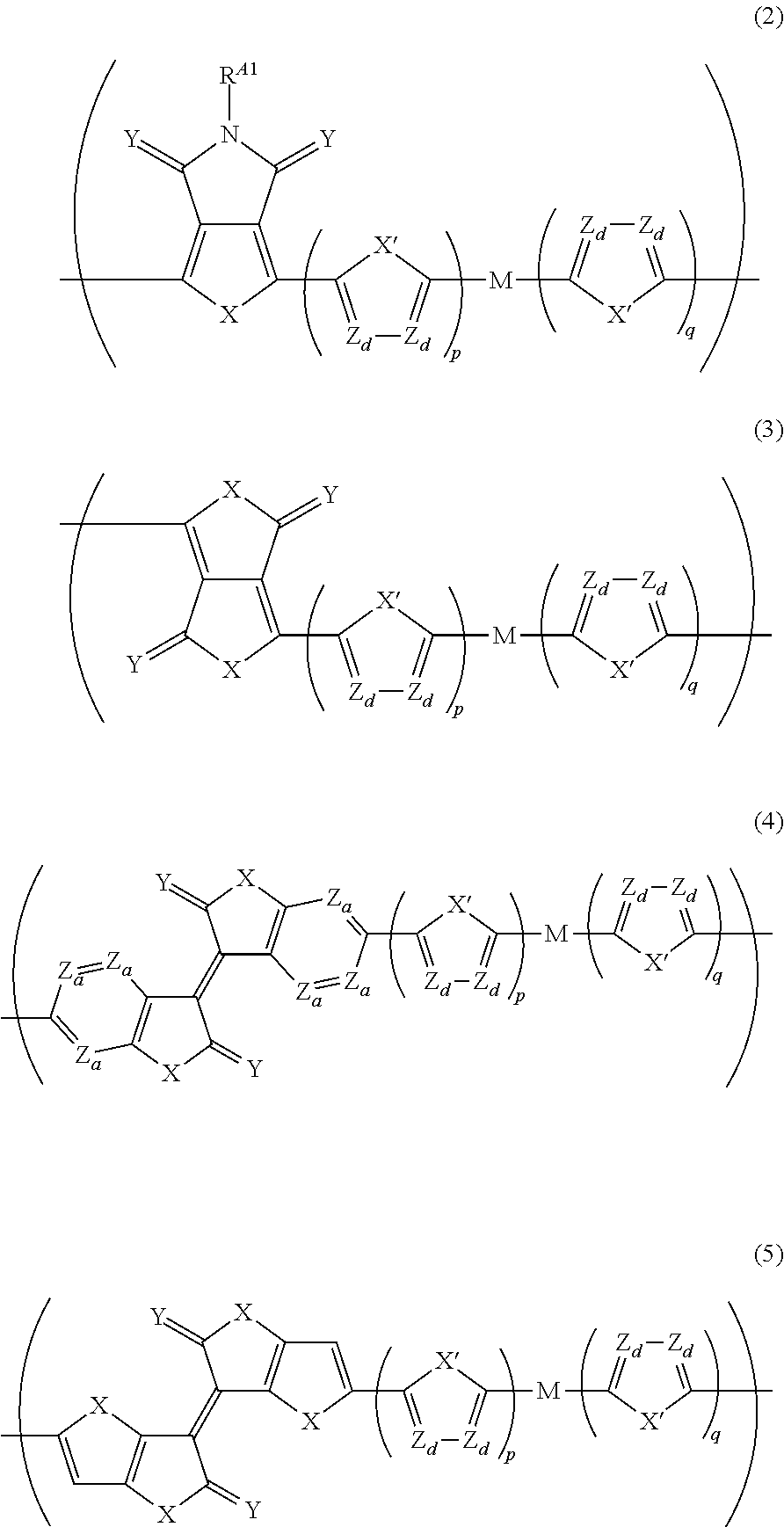
*-Ca-La-Ar


*-Ca-La-Ar


Applications Claiming Priority (3)
| Application Number | Priority Date | Filing Date | Title |
|---|---|---|---|
| JP2015-136448 | 2015-07-07 | ||
| JP2015136448 | 2015-07-07 | ||
| PCT/JP2016/068471 WO2017006765A1 (en) | 2015-07-07 | 2016-06-22 | Organic semiconductor element, compound, organic semiconductor composition, and method for producing organic semiconductor film |
Related Parent Applications (1)
| Application Number | Title | Priority Date | Filing Date |
|---|---|---|---|
| PCT/JP2016/068471 Continuation WO2017006765A1 (en) | 2015-07-07 | 2016-06-22 | Organic semiconductor element, compound, organic semiconductor composition, and method for producing organic semiconductor film |
Publications (2)
| Publication Number | Publication Date |
|---|---|
| US20180145259A1 US20180145259A1 (en) | 2018-05-24 |
| US10636975B2 true US10636975B2 (en) | 2020-04-28 |
Family
ID=57685034
Family Applications (1)
| Application Number | Title | Priority Date | Filing Date |
|---|---|---|---|
| US15/857,746 Active 2036-06-26 US10636975B2 (en) | 2015-07-07 | 2017-12-29 | Organic semiconductor element, compound, organic semiconductor composition, and method of manufacturing organic semiconductor film |
Country Status (4)
| Country | Link |
|---|---|
| US (1) | US10636975B2 (en) |
| JP (1) | JP6463475B2 (en) |
| TW (1) | TWI695852B (en) |
| WO (1) | WO2017006765A1 (en) |
Families Citing this family (2)
| Publication number | Priority date | Publication date | Assignee | Title |
|---|---|---|---|---|
| JP7086488B2 (en) * | 2017-03-21 | 2022-06-20 | 日本化薬株式会社 | Organic semiconductor compositions, organic thin films and organic thin films |
| US11302685B2 (en) * | 2017-11-17 | 2022-04-12 | Board Of Trustees Of Michigan State University | Fully-printed stretchable thin-film transistors and integrated logic circuits |
Citations (13)
| Publication number | Priority date | Publication date | Assignee | Title |
|---|---|---|---|---|
| JP2007516315A (en) | 2003-10-28 | 2007-06-21 | チバ スペシャルティ ケミカルズ ホールディング インコーポレーテッド | New diketopyrrolopyrrole polymer |
| JP2009541548A (en) | 2006-06-30 | 2009-11-26 | チバ ホールディング インコーポレーテッド | Diketopyrrolopyrrole polymers as organic semiconductors |
| JP2010018790A (en) | 2008-06-13 | 2010-01-28 | Sumitomo Chemical Co Ltd | Copolymer and polymer light-emitting element using the same |
| US20100099840A1 (en) | 2007-04-13 | 2010-04-22 | Jae-Min Moon | Dioxypyrrolo-heteroaromatic compounds and organic electronic devices using the same |
| JP2011501451A (en) | 2007-10-25 | 2011-01-06 | ビーエーエスエフ ソシエタス・ヨーロピア | Ketopyrroles as organic semiconductors |
| JP2011501743A (en) | 2007-10-09 | 2011-01-13 | ビーエーエスエフ ソシエタス・ヨーロピア | Pyrrolopyrrole derivatives, their manufacture and use |
| JP2011514399A (en) | 2008-02-05 | 2011-05-06 | ビーエーエスエフ ソシエタス・ヨーロピア | Naphthalene-imide semiconductor polymer |
| JP2012131938A (en) | 2009-12-25 | 2012-07-12 | Sumitomo Chemical Co Ltd | Polymer compound, and thin film and ink composition containing the same |
| TW201245266A (en) | 2011-03-11 | 2012-11-16 | Merck Patent Gmbh | Conjugated polymers |
| WO2012174561A2 (en) | 2011-06-17 | 2012-12-20 | The Regents Of The University Of California | REGIOREGULAR PYRIDAL[2,1,3]THIADIAZOLE π-CONJUGATED COPOLYMERS FOR ORGANIC SEMICONDUCTORS |
| JP2014507488A (en) | 2010-12-17 | 2014-03-27 | メルク パテント ゲゼルシャフト ミット ベシュレンクテル ハフツング | Conjugated polymer |
| JP2014237733A (en) | 2013-06-06 | 2014-12-18 | 住友化学株式会社 | Polymer compound and organic semiconductor element prepared using the same |
| WO2015076171A1 (en) | 2013-11-21 | 2015-05-28 | 株式会社ダイセル | Solvent for producing organic transistor |
Family Cites Families (2)
| Publication number | Priority date | Publication date | Assignee | Title |
|---|---|---|---|---|
| WO2010108873A1 (en) * | 2009-03-23 | 2010-09-30 | Basf Se | Diketopyrrolopyrrole polymers for use in organic semiconductor devices |
| JP6127789B2 (en) * | 2012-07-13 | 2017-05-17 | 三菱化学株式会社 | Copolymer, organic semiconductor material, organic electronic device and solar cell module |
-
2016
- 2016-06-22 JP JP2017527168A patent/JP6463475B2/en active Active
- 2016-06-22 WO PCT/JP2016/068471 patent/WO2017006765A1/en active Application Filing
- 2016-07-01 TW TW105120881A patent/TWI695852B/en active
-
2017
- 2017-12-29 US US15/857,746 patent/US10636975B2/en active Active
Patent Citations (26)
| Publication number | Priority date | Publication date | Assignee | Title |
|---|---|---|---|---|
| JP2007516315A (en) | 2003-10-28 | 2007-06-21 | チバ スペシャルティ ケミカルズ ホールディング インコーポレーテッド | New diketopyrrolopyrrole polymer |
| US7939818B2 (en) | 2003-10-28 | 2011-05-10 | Basf Se | Diketopyrrolopyrrole polymers |
| US20160049589A1 (en) | 2006-06-30 | 2016-02-18 | Basf Se | Diketopyrrolopyrrole polymers as organic semiconductors |
| JP2009541548A (en) | 2006-06-30 | 2009-11-26 | チバ ホールディング インコーポレーテッド | Diketopyrrolopyrrole polymers as organic semiconductors |
| US20100099840A1 (en) | 2007-04-13 | 2010-04-22 | Jae-Min Moon | Dioxypyrrolo-heteroaromatic compounds and organic electronic devices using the same |
| JP2010527327A (en) | 2007-04-13 | 2010-08-12 | エルジー・ケム・リミテッド | Heterocyclic compound containing dioxopyrrole ring and organic electronic device using the same |
| US9018397B2 (en) | 2007-10-09 | 2015-04-28 | Basf Se | Pyrrolopyrrole derivatives, their manufacture and use |
| JP2011501743A (en) | 2007-10-09 | 2011-01-13 | ビーエーエスエフ ソシエタス・ヨーロピア | Pyrrolopyrrole derivatives, their manufacture and use |
| US8758880B2 (en) | 2007-10-25 | 2014-06-24 | Basf Se | Ketopyrroles as organic semiconductors |
| JP2011501451A (en) | 2007-10-25 | 2011-01-06 | ビーエーエスエフ ソシエタス・ヨーロピア | Ketopyrroles as organic semiconductors |
| JP2011514913A (en) | 2008-02-05 | 2011-05-12 | ビーエーエスエフ ソシエタス・ヨーロピア | Semiconductor materials made from rylene- (π-acceptor) copolymers |
| US9219233B2 (en) | 2008-02-05 | 2015-12-22 | Basf Se | Semiconductor materials prepared from rylene-(π-acceptor)copolymers |
| JP2011514399A (en) | 2008-02-05 | 2011-05-06 | ビーエーエスエフ ソシエタス・ヨーロピア | Naphthalene-imide semiconductor polymer |
| US20110127512A1 (en) | 2008-06-13 | 2011-06-02 | Sumitomo Chemical Company, Limited | Copolymer and polymer light emitting device using the same |
| JP2010018790A (en) | 2008-06-13 | 2010-01-28 | Sumitomo Chemical Co Ltd | Copolymer and polymer light-emitting element using the same |
| US20120305899A1 (en) | 2009-12-25 | 2012-12-06 | National University Of Corporation Hiroshima University | Polymer compound, and thin film and ink composition each containing same |
| JP2012131938A (en) | 2009-12-25 | 2012-07-12 | Sumitomo Chemical Co Ltd | Polymer compound, and thin film and ink composition containing the same |
| JP2014507488A (en) | 2010-12-17 | 2014-03-27 | メルク パテント ゲゼルシャフト ミット ベシュレンクテル ハフツング | Conjugated polymer |
| US9048433B2 (en) | 2010-12-17 | 2015-06-02 | Merck Patent Gmbh | Conjugated polymers |
| TW201245266A (en) | 2011-03-11 | 2012-11-16 | Merck Patent Gmbh | Conjugated polymers |
| JP2014515043A (en) | 2011-03-11 | 2014-06-26 | メルク パテント ゲゼルシャフト ミット ベシュレンクテル ハフツング | Conjugated polymer |
| US20140001411A1 (en) | 2011-03-11 | 2014-01-02 | Merck Patent Gmbh | Conjugated polymers |
| WO2012174561A2 (en) | 2011-06-17 | 2012-12-20 | The Regents Of The University Of California | REGIOREGULAR PYRIDAL[2,1,3]THIADIAZOLE π-CONJUGATED COPOLYMERS FOR ORGANIC SEMICONDUCTORS |
| JP2014237733A (en) | 2013-06-06 | 2014-12-18 | 住友化学株式会社 | Polymer compound and organic semiconductor element prepared using the same |
| WO2015076171A1 (en) | 2013-11-21 | 2015-05-28 | 株式会社ダイセル | Solvent for producing organic transistor |
| US20160293849A1 (en) | 2013-11-21 | 2016-10-06 | Daicel Corporation | Solvent for producing organic transistor |
Non-Patent Citations (4)
| Title |
|---|
| An Office Action mailed by Taiwan Intellectual Property Office dated Jan. 22, 2020, which corresponds to Taiwanese Patent Application No. 105120881 and is related to U.S. Appl. No. 15/857,746. |
| International Search Report issued in PCT/JP2016/068471; dated Aug. 9, 2016. |
| Shi et al.; Alkylphenyl Substituted Naphthodithiophene: A New Building Unit with Conjugated Side Chains for Semiconducting Materials; Macromolecular Rapid Communications; vol. 35; 2014; pp. 1886-1889. |
| Written Opinion issued in PCT/JP2016/068471; dated Aug. 9, 2016. |
Also Published As
| Publication number | Publication date |
|---|---|
| TWI695852B (en) | 2020-06-11 |
| TW201708300A (en) | 2017-03-01 |
| JP6463475B2 (en) | 2019-02-06 |
| JPWO2017006765A1 (en) | 2018-04-12 |
| WO2017006765A1 (en) | 2017-01-12 |
| US20180145259A1 (en) | 2018-05-24 |
Similar Documents
| Publication | Publication Date | Title |
|---|---|---|
| US10312447B2 (en) | Organic semiconductor element, manufacturing method thereof, compound, organic semiconductor composition, organic semiconductor film, and manufacturing method thereof | |
| US20190036029A1 (en) | Organic thin film transistor element, organic semiconductor film-forming composition, method of forming organic semiconductor film, and organic semiconductor film | |
| US10971686B2 (en) | Organic semiconductor element, polymer, organic semiconductor composition, and organic semiconductor film | |
| US10636975B2 (en) | Organic semiconductor element, compound, organic semiconductor composition, and method of manufacturing organic semiconductor film | |
| US10902969B2 (en) | Organic semiconductor composition, organic semiconductor film, organic thin film transistor, and method of manufacturing organic thin film transistor | |
| JP6709275B2 (en) | Organic semiconductor film, organic semiconductor device, polymer and organic semiconductor composition | |
| US20180145258A1 (en) | Organic semiconductor element, compound, organic semiconductor composition, organic semiconductor film, and manufacturing method thereof | |
| US10217942B2 (en) | Organic semiconductor element, manufacturing method thereof, compound, composition for forming organic semiconductor film, and organic semiconductor film | |
| JP6573983B2 (en) | Composition for forming organic semiconductor film, compound, organic semiconductor film, organic semiconductor element | |
| US20170226280A1 (en) | Organic semiconductor element, manufacturing method thereof, compound, composition for forming organic semiconductor film, and organic semiconductor film | |
| JP2017054876A (en) | Organic semiconductor film-forming composition, organic semiconductor film, method for producing the same, and organic semiconductor element | |
| US9932441B2 (en) | Organic semiconductor element, manufacturing method thereof, compound, composition for forming organic semiconductor film, organic semiconductor film, and manufacturing method thereof | |
| JP6328791B2 (en) | Organic semiconductor device and compound | |
| US11038125B2 (en) | Organic semiconductor element, polymer, organic semiconductor composition, and organic semiconductor film |
Legal Events
| Date | Code | Title | Description |
|---|---|---|---|
| AS | Assignment |
Owner name: FUJIFILM CORPORATION, JAPAN Free format text: ASSIGNMENT OF ASSIGNORS INTEREST;ASSIGNORS:YAMAMOTO, YOSUKE;SHIGENOI, YUTA;REEL/FRAME:044503/0859 Effective date: 20171025 |
|
| FEPP | Fee payment procedure |
Free format text: ENTITY STATUS SET TO UNDISCOUNTED (ORIGINAL EVENT CODE: BIG.); ENTITY STATUS OF PATENT OWNER: LARGE ENTITY |
|
| STPP | Information on status: patent application and granting procedure in general |
Free format text: DOCKETED NEW CASE - READY FOR EXAMINATION |
|
| STPP | Information on status: patent application and granting procedure in general |
Free format text: NON FINAL ACTION MAILED |
|
| STPP | Information on status: patent application and granting procedure in general |
Free format text: RESPONSE TO NON-FINAL OFFICE ACTION ENTERED AND FORWARDED TO EXAMINER |
|
| STPP | Information on status: patent application and granting procedure in general |
Free format text: NOTICE OF ALLOWANCE MAILED -- APPLICATION RECEIVED IN OFFICE OF PUBLICATIONS |
|
| STCF | Information on status: patent grant |
Free format text: PATENTED CASE |
|
| MAFP | Maintenance fee payment |
Free format text: PAYMENT OF MAINTENANCE FEE, 4TH YEAR, LARGE ENTITY (ORIGINAL EVENT CODE: M1551); ENTITY STATUS OF PATENT OWNER: LARGE ENTITY Year of fee payment: 4 |