US10636894B2 - Fin-type transistors with spacers on the gates - Google Patents
Fin-type transistors with spacers on the gates Download PDFInfo
- Publication number
- US10636894B2 US10636894B2 US15/916,323 US201815916323A US10636894B2 US 10636894 B2 US10636894 B2 US 10636894B2 US 201815916323 A US201815916323 A US 201815916323A US 10636894 B2 US10636894 B2 US 10636894B2
- Authority
- US
- United States
- Prior art keywords
- spacers
- gate conductors
- source
- insulating spacers
- gate
- Prior art date
- Legal status (The legal status is an assumption and is not a legal conclusion. Google has not performed a legal analysis and makes no representation as to the accuracy of the status listed.)
- Active, expires
Links
- 125000006850 spacer group Chemical group 0.000 title claims abstract description 174
- 239000004020 conductor Substances 0.000 claims abstract description 120
- 239000004065 semiconductor Substances 0.000 claims abstract description 60
- 239000012212 insulator Substances 0.000 claims abstract description 42
- 239000000463 material Substances 0.000 claims abstract description 41
- 239000000758 substrate Substances 0.000 claims abstract description 24
- 238000000034 method Methods 0.000 abstract description 25
- 238000010586 diagram Methods 0.000 description 37
- 229910052751 metal Inorganic materials 0.000 description 9
- 239000002184 metal Substances 0.000 description 9
- 238000000059 patterning Methods 0.000 description 8
- 230000003071 parasitic effect Effects 0.000 description 7
- XUIMIQQOPSSXEZ-UHFFFAOYSA-N Silicon Chemical compound [Si] XUIMIQQOPSSXEZ-UHFFFAOYSA-N 0.000 description 4
- 230000015556 catabolic process Effects 0.000 description 4
- 238000006731 degradation reaction Methods 0.000 description 4
- 238000005530 etching Methods 0.000 description 4
- 230000006870 function Effects 0.000 description 4
- 239000012535 impurity Substances 0.000 description 4
- 150000004767 nitrides Chemical class 0.000 description 4
- 229910021420 polycrystalline silicon Inorganic materials 0.000 description 4
- 229910052710 silicon Inorganic materials 0.000 description 4
- 239000010703 silicon Substances 0.000 description 4
- 229920002120 photoresistant polymer Polymers 0.000 description 3
- 238000001020 plasma etching Methods 0.000 description 3
- 229920005591 polysilicon Polymers 0.000 description 3
- 235000012431 wafers Nutrition 0.000 description 3
- PXHVJJICTQNCMI-UHFFFAOYSA-N Nickel Chemical compound [Ni] PXHVJJICTQNCMI-UHFFFAOYSA-N 0.000 description 2
- 229910021417 amorphous silicon Inorganic materials 0.000 description 2
- 239000007795 chemical reaction product Substances 0.000 description 2
- 239000003989 dielectric material Substances 0.000 description 2
- 238000010292 electrical insulation Methods 0.000 description 2
- 238000005516 engineering process Methods 0.000 description 2
- 238000011065 in-situ storage Methods 0.000 description 2
- 238000002955 isolation Methods 0.000 description 2
- 150000002739 metals Chemical class 0.000 description 2
- 239000000047 product Substances 0.000 description 2
- WFKWXMTUELFFGS-UHFFFAOYSA-N tungsten Chemical compound [W] WFKWXMTUELFFGS-UHFFFAOYSA-N 0.000 description 2
- 229910052721 tungsten Inorganic materials 0.000 description 2
- 239000010937 tungsten Substances 0.000 description 2
- ZOXJGFHDIHLPTG-UHFFFAOYSA-N Boron Chemical compound [B] ZOXJGFHDIHLPTG-UHFFFAOYSA-N 0.000 description 1
- GYHNNYVSQQEPJS-UHFFFAOYSA-N Gallium Chemical compound [Ga] GYHNNYVSQQEPJS-UHFFFAOYSA-N 0.000 description 1
- ZOKXTWBITQBERF-UHFFFAOYSA-N Molybdenum Chemical compound [Mo] ZOKXTWBITQBERF-UHFFFAOYSA-N 0.000 description 1
- 229910052581 Si3N4 Inorganic materials 0.000 description 1
- RTAQQCXQSZGOHL-UHFFFAOYSA-N Titanium Chemical compound [Ti] RTAQQCXQSZGOHL-UHFFFAOYSA-N 0.000 description 1
- 229910045601 alloy Inorganic materials 0.000 description 1
- 239000000956 alloy Substances 0.000 description 1
- 230000004075 alteration Effects 0.000 description 1
- 229910052782 aluminium Inorganic materials 0.000 description 1
- XAGFODPZIPBFFR-UHFFFAOYSA-N aluminium Chemical compound [Al] XAGFODPZIPBFFR-UHFFFAOYSA-N 0.000 description 1
- 229910052787 antimony Inorganic materials 0.000 description 1
- WATWJIUSRGPENY-UHFFFAOYSA-N antimony atom Chemical compound [Sb] WATWJIUSRGPENY-UHFFFAOYSA-N 0.000 description 1
- 229910052785 arsenic Inorganic materials 0.000 description 1
- RQNWIZPPADIBDY-UHFFFAOYSA-N arsenic atom Chemical compound [As] RQNWIZPPADIBDY-UHFFFAOYSA-N 0.000 description 1
- QVGXLLKOCUKJST-UHFFFAOYSA-N atomic oxygen Chemical compound [O] QVGXLLKOCUKJST-UHFFFAOYSA-N 0.000 description 1
- 230000015572 biosynthetic process Effects 0.000 description 1
- 229910052796 boron Inorganic materials 0.000 description 1
- 239000003990 capacitor Substances 0.000 description 1
- 239000000919 ceramic Substances 0.000 description 1
- 229910010293 ceramic material Inorganic materials 0.000 description 1
- 239000013043 chemical agent Substances 0.000 description 1
- 238000005229 chemical vapour deposition Methods 0.000 description 1
- 230000000295 complement effect Effects 0.000 description 1
- 238000013500 data storage Methods 0.000 description 1
- 230000007423 decrease Effects 0.000 description 1
- 230000007812 deficiency Effects 0.000 description 1
- 230000001419 dependent effect Effects 0.000 description 1
- 238000000151 deposition Methods 0.000 description 1
- 239000002019 doping agent Substances 0.000 description 1
- 230000000694 effects Effects 0.000 description 1
- 230000005669 field effect Effects 0.000 description 1
- 229910052733 gallium Inorganic materials 0.000 description 1
- 239000007789 gas Substances 0.000 description 1
- 229910052732 germanium Inorganic materials 0.000 description 1
- 229910052735 hafnium Inorganic materials 0.000 description 1
- VBJZVLUMGGDVMO-UHFFFAOYSA-N hafnium atom Chemical compound [Hf] VBJZVLUMGGDVMO-UHFFFAOYSA-N 0.000 description 1
- BHEPBYXIRTUNPN-UHFFFAOYSA-N hydridophosphorus(.) (triplet) Chemical compound [PH] BHEPBYXIRTUNPN-UHFFFAOYSA-N 0.000 description 1
- 238000002513 implantation Methods 0.000 description 1
- 239000011810 insulating material Substances 0.000 description 1
- 239000013067 intermediate product Substances 0.000 description 1
- 238000005468 ion implantation Methods 0.000 description 1
- 230000000670 limiting effect Effects 0.000 description 1
- 230000000873 masking effect Effects 0.000 description 1
- 229910044991 metal oxide Inorganic materials 0.000 description 1
- 150000004706 metal oxides Chemical class 0.000 description 1
- 229910052750 molybdenum Inorganic materials 0.000 description 1
- 239000011733 molybdenum Substances 0.000 description 1
- 229910052759 nickel Inorganic materials 0.000 description 1
- 239000011368 organic material Substances 0.000 description 1
- 239000001301 oxygen Substances 0.000 description 1
- 229910052760 oxygen Inorganic materials 0.000 description 1
- 230000036961 partial effect Effects 0.000 description 1
- 238000005240 physical vapour deposition Methods 0.000 description 1
- 230000005855 radiation Effects 0.000 description 1
- 230000009467 reduction Effects 0.000 description 1
- 230000002829 reductive effect Effects 0.000 description 1
- 230000002441 reversible effect Effects 0.000 description 1
- 229910021332 silicide Inorganic materials 0.000 description 1
- FVBUAEGBCNSCDD-UHFFFAOYSA-N silicide(4-) Chemical compound [Si-4] FVBUAEGBCNSCDD-UHFFFAOYSA-N 0.000 description 1
- HQVNEWCFYHHQES-UHFFFAOYSA-N silicon nitride Chemical compound N12[Si]34N5[Si]62N3[Si]51N64 HQVNEWCFYHHQES-UHFFFAOYSA-N 0.000 description 1
- 239000000126 substance Substances 0.000 description 1
- 238000006467 substitution reaction Methods 0.000 description 1
- 229910052715 tantalum Inorganic materials 0.000 description 1
- GUVRBAGPIYLISA-UHFFFAOYSA-N tantalum atom Chemical compound [Ta] GUVRBAGPIYLISA-UHFFFAOYSA-N 0.000 description 1
- 239000010936 titanium Substances 0.000 description 1
- 229910052719 titanium Inorganic materials 0.000 description 1
- 238000001039 wet etching Methods 0.000 description 1
Images


Classifications
-
- H—ELECTRICITY
- H01—ELECTRIC ELEMENTS
- H01L—SEMICONDUCTOR DEVICES NOT COVERED BY CLASS H10
- H01L29/00—Semiconductor devices adapted for rectifying, amplifying, oscillating or switching, or capacitors or resistors with at least one potential-jump barrier or surface barrier, e.g. PN junction depletion layer or carrier concentration layer; Details of semiconductor bodies or of electrodes thereof ; Multistep manufacturing processes therefor
- H01L29/66—Types of semiconductor device ; Multistep manufacturing processes therefor
- H01L29/66007—Multistep manufacturing processes
- H01L29/66075—Multistep manufacturing processes of devices having semiconductor bodies comprising group 14 or group 13/15 materials
- H01L29/66227—Multistep manufacturing processes of devices having semiconductor bodies comprising group 14 or group 13/15 materials the devices being controllable only by the electric current supplied or the electric potential applied, to an electrode which does not carry the current to be rectified, amplified or switched, e.g. three-terminal devices
- H01L29/66409—Unipolar field-effect transistors
- H01L29/66477—Unipolar field-effect transistors with an insulated gate, i.e. MISFET
- H01L29/66553—Unipolar field-effect transistors with an insulated gate, i.e. MISFET using inside spacers, permanent or not
-
- H—ELECTRICITY
- H01—ELECTRIC ELEMENTS
- H01L—SEMICONDUCTOR DEVICES NOT COVERED BY CLASS H10
- H01L21/00—Processes or apparatus adapted for the manufacture or treatment of semiconductor or solid state devices or of parts thereof
- H01L21/70—Manufacture or treatment of devices consisting of a plurality of solid state components formed in or on a common substrate or of parts thereof; Manufacture of integrated circuit devices or of parts thereof
- H01L21/77—Manufacture or treatment of devices consisting of a plurality of solid state components or integrated circuits formed in, or on, a common substrate
- H01L21/78—Manufacture or treatment of devices consisting of a plurality of solid state components or integrated circuits formed in, or on, a common substrate with subsequent division of the substrate into plural individual devices
- H01L21/82—Manufacture or treatment of devices consisting of a plurality of solid state components or integrated circuits formed in, or on, a common substrate with subsequent division of the substrate into plural individual devices to produce devices, e.g. integrated circuits, each consisting of a plurality of components
- H01L21/822—Manufacture or treatment of devices consisting of a plurality of solid state components or integrated circuits formed in, or on, a common substrate with subsequent division of the substrate into plural individual devices to produce devices, e.g. integrated circuits, each consisting of a plurality of components the substrate being a semiconductor, using silicon technology
- H01L21/8232—Field-effect technology
- H01L21/8234—MIS technology, i.e. integration processes of field effect transistors of the conductor-insulator-semiconductor type
- H01L21/8238—Complementary field-effect transistors, e.g. CMOS
- H01L21/823814—Complementary field-effect transistors, e.g. CMOS with a particular manufacturing method of the source or drain structures, e.g. specific source or drain implants or silicided source or drain structures or raised source or drain structures
-
- H—ELECTRICITY
- H01—ELECTRIC ELEMENTS
- H01L—SEMICONDUCTOR DEVICES NOT COVERED BY CLASS H10
- H01L21/00—Processes or apparatus adapted for the manufacture or treatment of semiconductor or solid state devices or of parts thereof
- H01L21/70—Manufacture or treatment of devices consisting of a plurality of solid state components formed in or on a common substrate or of parts thereof; Manufacture of integrated circuit devices or of parts thereof
- H01L21/77—Manufacture or treatment of devices consisting of a plurality of solid state components or integrated circuits formed in, or on, a common substrate
- H01L21/78—Manufacture or treatment of devices consisting of a plurality of solid state components or integrated circuits formed in, or on, a common substrate with subsequent division of the substrate into plural individual devices
- H01L21/82—Manufacture or treatment of devices consisting of a plurality of solid state components or integrated circuits formed in, or on, a common substrate with subsequent division of the substrate into plural individual devices to produce devices, e.g. integrated circuits, each consisting of a plurality of components
- H01L21/822—Manufacture or treatment of devices consisting of a plurality of solid state components or integrated circuits formed in, or on, a common substrate with subsequent division of the substrate into plural individual devices to produce devices, e.g. integrated circuits, each consisting of a plurality of components the substrate being a semiconductor, using silicon technology
- H01L21/8232—Field-effect technology
- H01L21/8234—MIS technology, i.e. integration processes of field effect transistors of the conductor-insulator-semiconductor type
- H01L21/8238—Complementary field-effect transistors, e.g. CMOS
- H01L21/823821—Complementary field-effect transistors, e.g. CMOS with a particular manufacturing method of transistors with a horizontal current flow in a vertical sidewall of a semiconductor body, e.g. FinFET, MuGFET
-
- H—ELECTRICITY
- H01—ELECTRIC ELEMENTS
- H01L—SEMICONDUCTOR DEVICES NOT COVERED BY CLASS H10
- H01L21/00—Processes or apparatus adapted for the manufacture or treatment of semiconductor or solid state devices or of parts thereof
- H01L21/70—Manufacture or treatment of devices consisting of a plurality of solid state components formed in or on a common substrate or of parts thereof; Manufacture of integrated circuit devices or of parts thereof
- H01L21/77—Manufacture or treatment of devices consisting of a plurality of solid state components or integrated circuits formed in, or on, a common substrate
- H01L21/78—Manufacture or treatment of devices consisting of a plurality of solid state components or integrated circuits formed in, or on, a common substrate with subsequent division of the substrate into plural individual devices
- H01L21/82—Manufacture or treatment of devices consisting of a plurality of solid state components or integrated circuits formed in, or on, a common substrate with subsequent division of the substrate into plural individual devices to produce devices, e.g. integrated circuits, each consisting of a plurality of components
- H01L21/822—Manufacture or treatment of devices consisting of a plurality of solid state components or integrated circuits formed in, or on, a common substrate with subsequent division of the substrate into plural individual devices to produce devices, e.g. integrated circuits, each consisting of a plurality of components the substrate being a semiconductor, using silicon technology
- H01L21/8232—Field-effect technology
- H01L21/8234—MIS technology, i.e. integration processes of field effect transistors of the conductor-insulator-semiconductor type
- H01L21/8238—Complementary field-effect transistors, e.g. CMOS
- H01L21/823864—Complementary field-effect transistors, e.g. CMOS with a particular manufacturing method of the gate sidewall spacers, e.g. double spacers, particular spacer material or shape
-
- H—ELECTRICITY
- H01—ELECTRIC ELEMENTS
- H01L—SEMICONDUCTOR DEVICES NOT COVERED BY CLASS H10
- H01L27/00—Devices consisting of a plurality of semiconductor or other solid-state components formed in or on a common substrate
- H01L27/02—Devices consisting of a plurality of semiconductor or other solid-state components formed in or on a common substrate including semiconductor components specially adapted for rectifying, oscillating, amplifying or switching and having at least one potential-jump barrier or surface barrier; including integrated passive circuit elements with at least one potential-jump barrier or surface barrier
- H01L27/04—Devices consisting of a plurality of semiconductor or other solid-state components formed in or on a common substrate including semiconductor components specially adapted for rectifying, oscillating, amplifying or switching and having at least one potential-jump barrier or surface barrier; including integrated passive circuit elements with at least one potential-jump barrier or surface barrier the substrate being a semiconductor body
- H01L27/08—Devices consisting of a plurality of semiconductor or other solid-state components formed in or on a common substrate including semiconductor components specially adapted for rectifying, oscillating, amplifying or switching and having at least one potential-jump barrier or surface barrier; including integrated passive circuit elements with at least one potential-jump barrier or surface barrier the substrate being a semiconductor body including only semiconductor components of a single kind
- H01L27/085—Devices consisting of a plurality of semiconductor or other solid-state components formed in or on a common substrate including semiconductor components specially adapted for rectifying, oscillating, amplifying or switching and having at least one potential-jump barrier or surface barrier; including integrated passive circuit elements with at least one potential-jump barrier or surface barrier the substrate being a semiconductor body including only semiconductor components of a single kind including field-effect components only
- H01L27/088—Devices consisting of a plurality of semiconductor or other solid-state components formed in or on a common substrate including semiconductor components specially adapted for rectifying, oscillating, amplifying or switching and having at least one potential-jump barrier or surface barrier; including integrated passive circuit elements with at least one potential-jump barrier or surface barrier the substrate being a semiconductor body including only semiconductor components of a single kind including field-effect components only the components being field-effect transistors with insulated gate
- H01L27/092—Devices consisting of a plurality of semiconductor or other solid-state components formed in or on a common substrate including semiconductor components specially adapted for rectifying, oscillating, amplifying or switching and having at least one potential-jump barrier or surface barrier; including integrated passive circuit elements with at least one potential-jump barrier or surface barrier the substrate being a semiconductor body including only semiconductor components of a single kind including field-effect components only the components being field-effect transistors with insulated gate complementary MIS field-effect transistors
- H01L27/0924—Devices consisting of a plurality of semiconductor or other solid-state components formed in or on a common substrate including semiconductor components specially adapted for rectifying, oscillating, amplifying or switching and having at least one potential-jump barrier or surface barrier; including integrated passive circuit elements with at least one potential-jump barrier or surface barrier the substrate being a semiconductor body including only semiconductor components of a single kind including field-effect components only the components being field-effect transistors with insulated gate complementary MIS field-effect transistors including transistors with a horizontal current flow in a vertical sidewall of a semiconductor body, e.g. FinFET, MuGFET
-
- H—ELECTRICITY
- H01—ELECTRIC ELEMENTS
- H01L—SEMICONDUCTOR DEVICES NOT COVERED BY CLASS H10
- H01L29/00—Semiconductor devices adapted for rectifying, amplifying, oscillating or switching, or capacitors or resistors with at least one potential-jump barrier or surface barrier, e.g. PN junction depletion layer or carrier concentration layer; Details of semiconductor bodies or of electrodes thereof ; Multistep manufacturing processes therefor
- H01L29/66—Types of semiconductor device ; Multistep manufacturing processes therefor
- H01L29/66007—Multistep manufacturing processes
- H01L29/66075—Multistep manufacturing processes of devices having semiconductor bodies comprising group 14 or group 13/15 materials
- H01L29/66227—Multistep manufacturing processes of devices having semiconductor bodies comprising group 14 or group 13/15 materials the devices being controllable only by the electric current supplied or the electric potential applied, to an electrode which does not carry the current to be rectified, amplified or switched, e.g. three-terminal devices
- H01L29/66409—Unipolar field-effect transistors
- H01L29/66477—Unipolar field-effect transistors with an insulated gate, i.e. MISFET
- H01L29/66545—Unipolar field-effect transistors with an insulated gate, i.e. MISFET using a dummy, i.e. replacement gate in a process wherein at least a part of the final gate is self aligned to the dummy gate
-
- H—ELECTRICITY
- H01—ELECTRIC ELEMENTS
- H01L—SEMICONDUCTOR DEVICES NOT COVERED BY CLASS H10
- H01L29/00—Semiconductor devices adapted for rectifying, amplifying, oscillating or switching, or capacitors or resistors with at least one potential-jump barrier or surface barrier, e.g. PN junction depletion layer or carrier concentration layer; Details of semiconductor bodies or of electrodes thereof ; Multistep manufacturing processes therefor
- H01L29/66—Types of semiconductor device ; Multistep manufacturing processes therefor
- H01L29/66007—Multistep manufacturing processes
- H01L29/66075—Multistep manufacturing processes of devices having semiconductor bodies comprising group 14 or group 13/15 materials
- H01L29/66227—Multistep manufacturing processes of devices having semiconductor bodies comprising group 14 or group 13/15 materials the devices being controllable only by the electric current supplied or the electric potential applied, to an electrode which does not carry the current to be rectified, amplified or switched, e.g. three-terminal devices
- H01L29/66409—Unipolar field-effect transistors
- H01L29/66477—Unipolar field-effect transistors with an insulated gate, i.e. MISFET
- H01L29/6656—Unipolar field-effect transistors with an insulated gate, i.e. MISFET using multiple spacer layers, e.g. multiple sidewall spacers
-
- H—ELECTRICITY
- H01—ELECTRIC ELEMENTS
- H01L—SEMICONDUCTOR DEVICES NOT COVERED BY CLASS H10
- H01L29/00—Semiconductor devices adapted for rectifying, amplifying, oscillating or switching, or capacitors or resistors with at least one potential-jump barrier or surface barrier, e.g. PN junction depletion layer or carrier concentration layer; Details of semiconductor bodies or of electrodes thereof ; Multistep manufacturing processes therefor
- H01L29/66—Types of semiconductor device ; Multistep manufacturing processes therefor
- H01L29/66007—Multistep manufacturing processes
- H01L29/66075—Multistep manufacturing processes of devices having semiconductor bodies comprising group 14 or group 13/15 materials
- H01L29/66227—Multistep manufacturing processes of devices having semiconductor bodies comprising group 14 or group 13/15 materials the devices being controllable only by the electric current supplied or the electric potential applied, to an electrode which does not carry the current to be rectified, amplified or switched, e.g. three-terminal devices
- H01L29/66409—Unipolar field-effect transistors
- H01L29/66477—Unipolar field-effect transistors with an insulated gate, i.e. MISFET
- H01L29/66787—Unipolar field-effect transistors with an insulated gate, i.e. MISFET with a gate at the side of the channel
- H01L29/66795—Unipolar field-effect transistors with an insulated gate, i.e. MISFET with a gate at the side of the channel with a horizontal current flow in a vertical sidewall of a semiconductor body, e.g. FinFET, MuGFET
-
- H—ELECTRICITY
- H01—ELECTRIC ELEMENTS
- H01L—SEMICONDUCTOR DEVICES NOT COVERED BY CLASS H10
- H01L29/00—Semiconductor devices adapted for rectifying, amplifying, oscillating or switching, or capacitors or resistors with at least one potential-jump barrier or surface barrier, e.g. PN junction depletion layer or carrier concentration layer; Details of semiconductor bodies or of electrodes thereof ; Multistep manufacturing processes therefor
- H01L29/66—Types of semiconductor device ; Multistep manufacturing processes therefor
- H01L29/68—Types of semiconductor device ; Multistep manufacturing processes therefor controllable by only the electric current supplied, or only the electric potential applied, to an electrode which does not carry the current to be rectified, amplified or switched
- H01L29/76—Unipolar devices, e.g. field effect transistors
- H01L29/772—Field effect transistors
- H01L29/78—Field effect transistors with field effect produced by an insulated gate
- H01L29/785—Field effect transistors with field effect produced by an insulated gate having a channel with a horizontal current flow in a vertical sidewall of a semiconductor body, e.g. FinFET, MuGFET
-
- H—ELECTRICITY
- H01—ELECTRIC ELEMENTS
- H01L—SEMICONDUCTOR DEVICES NOT COVERED BY CLASS H10
- H01L21/00—Processes or apparatus adapted for the manufacture or treatment of semiconductor or solid state devices or of parts thereof
- H01L21/70—Manufacture or treatment of devices consisting of a plurality of solid state components formed in or on a common substrate or of parts thereof; Manufacture of integrated circuit devices or of parts thereof
- H01L21/77—Manufacture or treatment of devices consisting of a plurality of solid state components or integrated circuits formed in, or on, a common substrate
- H01L21/78—Manufacture or treatment of devices consisting of a plurality of solid state components or integrated circuits formed in, or on, a common substrate with subsequent division of the substrate into plural individual devices
- H01L21/82—Manufacture or treatment of devices consisting of a plurality of solid state components or integrated circuits formed in, or on, a common substrate with subsequent division of the substrate into plural individual devices to produce devices, e.g. integrated circuits, each consisting of a plurality of components
- H01L21/822—Manufacture or treatment of devices consisting of a plurality of solid state components or integrated circuits formed in, or on, a common substrate with subsequent division of the substrate into plural individual devices to produce devices, e.g. integrated circuits, each consisting of a plurality of components the substrate being a semiconductor, using silicon technology
- H01L21/8232—Field-effect technology
- H01L21/8234—MIS technology, i.e. integration processes of field effect transistors of the conductor-insulator-semiconductor type
- H01L21/823431—MIS technology, i.e. integration processes of field effect transistors of the conductor-insulator-semiconductor type with a particular manufacturing method of transistors with a horizontal current flow in a vertical sidewall of a semiconductor body, e.g. FinFET, MuGFET
-
- H—ELECTRICITY
- H01—ELECTRIC ELEMENTS
- H01L—SEMICONDUCTOR DEVICES NOT COVERED BY CLASS H10
- H01L21/00—Processes or apparatus adapted for the manufacture or treatment of semiconductor or solid state devices or of parts thereof
- H01L21/70—Manufacture or treatment of devices consisting of a plurality of solid state components formed in or on a common substrate or of parts thereof; Manufacture of integrated circuit devices or of parts thereof
- H01L21/77—Manufacture or treatment of devices consisting of a plurality of solid state components or integrated circuits formed in, or on, a common substrate
- H01L21/78—Manufacture or treatment of devices consisting of a plurality of solid state components or integrated circuits formed in, or on, a common substrate with subsequent division of the substrate into plural individual devices
- H01L21/82—Manufacture or treatment of devices consisting of a plurality of solid state components or integrated circuits formed in, or on, a common substrate with subsequent division of the substrate into plural individual devices to produce devices, e.g. integrated circuits, each consisting of a plurality of components
- H01L21/822—Manufacture or treatment of devices consisting of a plurality of solid state components or integrated circuits formed in, or on, a common substrate with subsequent division of the substrate into plural individual devices to produce devices, e.g. integrated circuits, each consisting of a plurality of components the substrate being a semiconductor, using silicon technology
- H01L21/8232—Field-effect technology
- H01L21/8234—MIS technology, i.e. integration processes of field effect transistors of the conductor-insulator-semiconductor type
- H01L21/823468—MIS technology, i.e. integration processes of field effect transistors of the conductor-insulator-semiconductor type with a particular manufacturing method of the gate sidewall spacers, e.g. double spacers, particular spacer material or shape
-
- H—ELECTRICITY
- H01—ELECTRIC ELEMENTS
- H01L—SEMICONDUCTOR DEVICES NOT COVERED BY CLASS H10
- H01L27/00—Devices consisting of a plurality of semiconductor or other solid-state components formed in or on a common substrate
- H01L27/02—Devices consisting of a plurality of semiconductor or other solid-state components formed in or on a common substrate including semiconductor components specially adapted for rectifying, oscillating, amplifying or switching and having at least one potential-jump barrier or surface barrier; including integrated passive circuit elements with at least one potential-jump barrier or surface barrier
- H01L27/04—Devices consisting of a plurality of semiconductor or other solid-state components formed in or on a common substrate including semiconductor components specially adapted for rectifying, oscillating, amplifying or switching and having at least one potential-jump barrier or surface barrier; including integrated passive circuit elements with at least one potential-jump barrier or surface barrier the substrate being a semiconductor body
- H01L27/08—Devices consisting of a plurality of semiconductor or other solid-state components formed in or on a common substrate including semiconductor components specially adapted for rectifying, oscillating, amplifying or switching and having at least one potential-jump barrier or surface barrier; including integrated passive circuit elements with at least one potential-jump barrier or surface barrier the substrate being a semiconductor body including only semiconductor components of a single kind
- H01L27/085—Devices consisting of a plurality of semiconductor or other solid-state components formed in or on a common substrate including semiconductor components specially adapted for rectifying, oscillating, amplifying or switching and having at least one potential-jump barrier or surface barrier; including integrated passive circuit elements with at least one potential-jump barrier or surface barrier the substrate being a semiconductor body including only semiconductor components of a single kind including field-effect components only
- H01L27/088—Devices consisting of a plurality of semiconductor or other solid-state components formed in or on a common substrate including semiconductor components specially adapted for rectifying, oscillating, amplifying or switching and having at least one potential-jump barrier or surface barrier; including integrated passive circuit elements with at least one potential-jump barrier or surface barrier the substrate being a semiconductor body including only semiconductor components of a single kind including field-effect components only the components being field-effect transistors with insulated gate
- H01L27/0886—Devices consisting of a plurality of semiconductor or other solid-state components formed in or on a common substrate including semiconductor components specially adapted for rectifying, oscillating, amplifying or switching and having at least one potential-jump barrier or surface barrier; including integrated passive circuit elements with at least one potential-jump barrier or surface barrier the substrate being a semiconductor body including only semiconductor components of a single kind including field-effect components only the components being field-effect transistors with insulated gate including transistors with a horizontal current flow in a vertical sidewall of a semiconductor body, e.g. FinFET, MuGFET
Definitions
- the present disclosure relates to integrated circuit structures and methods, and more specifically, to methods that form fin-type transistors with spacers between the gates and adjacent contacts.
- a fin of a fin-type transistor is a thin, long, six-sided rectangle that extends from a substrate, with sides that are longer than they are wide, a top and bottom that have the same length as the sides (but that have a width that is much more narrow), and ends that are as tall from the substrate as the width of the sides, but that are only as wide as the as the top and bottom.
- Various methods herein pattern a substrate to form semiconductor fins extending from the substrate. Gate insulators are then formed/grown on the channel regions of the semiconductor fins, and sacrificial gates are formed/patterned on the gate insulators, adjacent the channel regions. The sacrificial gates are patterned to be perpendicular to the semiconductor fins, and to thereby intersect the semiconductor fins (but separated from the semiconductor fins by the gate insulators).
- first and second insulating spacers e.g., low-K insulators
- first and second insulating spacers e.g., low-K insulators
- second insulating spacers to leave the second insulating spacers only on the first insulating spacers in locations between where the sacrificial gates intersect the semiconductor fins.
- These methods replace the sacrificial gates with gate conductors, and form source/drain conductive contacts to the epitaxial source/drain material.
- the second insulating spacers contact either the source/drain conductive contacts or the gate conductors.
- the first insulating spacers and the second insulating spacers are on both sides of the gate conductors.
- the process of patterning the second insulating spacers causes both the first insulating spacers and the second insulating spacers to separate the gate conductors and the source/drain conductive contacts in the locations between where the gate conductors intersect the semiconductor fins, but only the first insulating spacers separate the gate conductors and the source/drain conductive contacts in the locations where the gate conductors intersect the semiconductor fins.
- the first insulating spacers and the second insulating spacers together cause a greater spacing around the gate conductors (e.g., between the gate conductors and the source/drain conductive contacts), relative to the first insulating spacers alone. Also, the process of patterning the second insulating spacers causes the first insulating spacers to continuously contact the gate conductors along the full length of the gate conductors, and the second insulating spacers to discontinuously contact the first insulating spacers along the full length of the gate conductors.
- Various structures herein include (among other components) semiconductor fins extending from a substrate, gate insulators contacting channel regions of the semiconductor fins, and gate conductors positioned adjacent the channel regions and contacting the gate insulators. Additionally, epitaxial source/drain material contacts the semiconductor fins on opposite sides of the channel regions, and source/drain conductive contacts contact the epitaxial source/drain material.
- first insulating spacers are on the gate conductors.
- the gate conductors are linear conductors perpendicular to the semiconductor fins, and the first insulating spacers are on both sides of the gate conductors.
- second insulating spacers are on the first insulating spacers; however, the second insulating spacers are only on the first insulating spacers in locations between where the gate conductors intersect the semiconductor fins.
- the first insulating spacers and the second insulating spacers are low-K insulators, and in different embodiments, the second insulating spacers contact either the source/drain conductive contacts or the gate conductors.
- the first insulating spacers and the second insulating spacers can be either the same insulator, or different insulators.
- both the first insulating spacers and the second insulating spacers separate the gate conductors and the source/drain conductive contacts in the locations between where the gate conductors intersect the semiconductor fins, but only the first insulating spacers separate the gate conductors and the source/drain conductive contacts in the locations where the gate conductors intersect the semiconductor fins.
- the first insulating spacers continuously contact the gate conductors along full lengths of the gate conductors, and wherein the second insulating spacers discontinuously contact the first insulating spacers along the along full lengths of the gate conductors.
- FIG. 1A is a top-view schematic diagram illustrating an integrated circuit structure according to embodiments herein;
- FIGS. 1B-1D are side-view schematic diagrams illustrating the integrated circuit structure shown in FIG. 1A along different cross-sections;
- FIG. 2A is a top-view schematic diagram illustrating an integrated circuit structure according to embodiments herein;
- FIGS. 2B-2D are side-view schematic diagrams illustrating the integrated circuit structure shown in FIG. 2A along different cross-sections;
- FIG. 3A is a top-view schematic diagram illustrating an integrated circuit structure according to embodiments herein;
- FIGS. 3B-3D are side-view schematic diagrams illustrating the integrated circuit structure shown in FIG. 3A along different cross-sections;
- FIG. 4A is a top-view schematic diagram illustrating an integrated circuit structure according to embodiments herein;
- FIGS. 4B-4D are side-view schematic diagrams illustrating the integrated circuit structure shown in FIG. 4A along different cross-sections;
- FIG. 5A is a top-view schematic diagram illustrating an integrated circuit structure according to embodiments herein;
- FIGS. 5B-5D are side-view schematic diagrams illustrating the integrated circuit structure shown in FIG. 5A along different cross-sections;
- FIG. 6 is a flow diagram illustrating the processing shown in FIGS. 1A-5D ;
- FIGS. 7A and 7B are perspective schematic diagrams illustrating the integrated circuit structure shown in FIG. 5A-5D
- FIG. 8A is a top-view schematic diagram illustrating an integrated circuit structure according to embodiments herein;
- FIGS. 8B-8D are side-view schematic diagrams illustrating the integrated circuit structure shown in FIG. 8A along different cross-sections;
- FIG. 9A is a top-view schematic diagram illustrating an integrated circuit structure according to embodiments herein;
- FIGS. 9B-9D are side-view schematic diagrams illustrating the integrated circuit structure shown in FIG. 9A along different cross-sections;
- FIG. 10A is a top-view schematic diagram illustrating an integrated circuit structure according to embodiments herein;
- FIGS. 10B-10D are side-view schematic diagrams illustrating the integrated circuit structure shown in FIG. 10A along different cross-sections;
- FIG. 11A is a top-view schematic diagram illustrating an integrated circuit structure according to embodiments herein;
- FIGS. 11B-11D are side-view schematic diagrams illustrating the integrated circuit structure shown in FIG. 11A along different cross-sections;
- FIG. 12A is a top-view schematic diagram illustrating an integrated circuit structure according to embodiments herein;
- FIGS. 12B-12D are side-view schematic diagrams illustrating the integrated circuit structure shown in FIG. 12A along different cross-sections;
- FIG. 13A is a top-view schematic diagram illustrating an integrated circuit structure according to embodiments herein;
- FIGS. 13B-13D are side-view schematic diagrams illustrating the integrated circuit structure shown in FIG. 13A along different cross-sections;
- FIG. 14 is a flow diagram illustrating the processing shown in FIGS. 1A-5D ;
- FIGS. 15A and 15B are perspective schematic diagrams illustrating the integrated circuit structure shown in FIG. 13A-13D .
- FET parasitic capacitance e.g., capacitance between gate to epi-source/drain and gate-to-through silicon via (TS), etc.
- SAC self-align-contact
- the gate is very close to the source/drain contact (e.g., the TS), and structures are only separated by spacers. A thicker spacer can significantly reduce the parasitic capacitance; however, an increase in spacer thickness decreases DC performance.
- FEOL processing involves the actual making of chip layers that have active devices, such as transistors, diodes, resistors, capacitors, etc., and is performed before the back end of line (BEOL) processing which forms power and signal connections to the FEOL devices.
- BEOL back end of line
- processing herein uses two spacers (one continuous, one discontinuous) to separate the metal gate and the source/drain contact, to reduce FEOL parasitic capacitance, without DC performance degradation. Therefore, in some locations two spacers are present between the metal gate and the source/drain contact, while in other locations (where the gate intersects the fin) only one spacer is present between the metal gate and the source/drain contact.
- the spacers are generally low-K insulators, and can be formed of the same material or different materials.
- an outer spacer is discontinuous and is not present in locations where the gates intersect the fins (but is present along the portions of the gate conductor that are between the fins).
- the inner spacer is discontinuous, in the same locations. Where both spacers are present (in areas away from the fins (e.g., between the fins)), this double-spacer structure increases the amount of electrical insulation between the gate and the through silicon via source/drain contact (to reduce parasitic capacitance); however, where only one spacer is present (in areas where the gate intersects the fin) the structure does not increase the amount of electrical insulation, which allows the gate conductor to have unreduced effect on the channel region of the fin, to avoid affecting DC performance.
- FIGS. 1A-6 illustrate various methods herein. More specifically, FIG. 6 is a flow diagram illustrating the processing shown in FIGS. 1A-5D , FIGS. 1A, 2A, 3A, 4A, and 5A are top-view schematic diagrams illustrating an integrated circuit structure according to embodiments herein, FIGS. 1B, 2B, 3B, 4B, and 5B are side-view schematic diagrams illustrating the integrated circuit structure shown in FIGS. 1A, 2A, 3A, 4A, and 5A along cross-section Y-Y, FIGS. 1C, 2C, 3C, 4C, and 5C are side-view schematic diagrams illustrating the integrated circuit structure shown in FIGS.
- FIGS. 1D, 2D, 3D, 4D, and 5D are side-view schematic diagrams illustrating the integrated circuit structure shown in FIGS. 1A, 2A, 3A, 4A, and 5A along cross-section X 2 -X 2 .
- these methods pattern a substrate 110 (e.g., silicon substrate, that can be doped or an in-situ semiconductor) to form semiconductor fins 102 extending from the substrate 110 , and form an insulator (e.g., oxide) 104 around the fins, as most clearly shown in FIGS. 1A-1B .
- a substrate 110 e.g., silicon substrate, that can be doped or an in-situ semiconductor
- an insulator e.g., oxide
- 1C-1D which can be, for example, polysilicon, are formed/patterned on the gate insulators 116 , adjacent the channel regions 132 in item 204 .
- the sacrificial gates 114 which are below the overlying gate caps 106 (e.g., silicon nitride) are patterned in item 204 to be perpendicular to the semiconductor fins 102 , and to thereby intersect the semiconductor fins 102 (but are separated from the semiconductor fins 102 by the gate insulators 116 ).
- first insulating spacers 108 such as a nitride, or other low-K material
- second insulating spacers 120 such as an oxide, or other low-K material
- photoresist masks 122 are used to pattern the second insulating spacers 120 in item 210 .
- first and second insulating spacers 108 and 120 can be different low-K insulators, allowing the second insulating spacers 108 to be selectively removed, without affecting the first insulating spacers 108 .
- the mask 122 is removed, as shown in FIGS. 4A-4D , this leaves the second insulating spacers 120 only on the first insulating spacers 108 in locations between where the sacrificial gates 114 intersect the semiconductor fins 102 .
- such methods epitaxially grow source/drain material 130 on the semiconductor fins 102 on opposite sides of the channel regions 132 .
- These methods also replace the sacrificial gates 114 with gate conductors 124 (e.g., metal, such as tungsten) in item 214 , and form source/drain conductive contacts 126 to the epitaxial source/drain material 130 in item 216 .
- gate conductors 124 e.g., metal, such as tungsten
- the first insulating spacers 108 and the second insulating spacers 120 are between the gate conductors 124 and the source/drain conductive contacts 126 .
- the process of patterning the second insulating spacers 120 in item 210 FIGS. 5A-5D .
- 3A-3D causes both the first insulating spacers 108 and the second insulating spacers 120 to separate the gate conductors 124 and the source/drain conductive contacts 126 in the locations between where the gate conductors 124 intersect the semiconductor fins 102 , but only the first insulating spacers 108 to separate the gate conductors 124 and the source/drain conductive contacts 126 in the locations where the gate conductors 124 intersect the semiconductor fins 102 .
- the first insulating spacers 108 and the second insulating spacers 120 together cause a greater spacing on the sides of the gate conductors 124 (e.g., between the gate conductors 124 and the source/drain conductive contacts 126 ), relative to the spacing provided by the first insulating spacers 108 alone.
- the process of patterning the second insulating spacers 120 in item 210 causes the first insulating spacers 108 to continuously contact the gate conductors 124 along the full length of the gate conductors 124 , and the second insulating spacers 120 to discontinuously contact the first insulating spacers 108 along the full length of the gate conductors 124 .
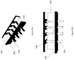
- FIGS. 7A and 7B are perspective schematic diagrams illustrating the gate conductors 124 with the continuous spacer 108 , and the discontinuous spacer 120 and the fins 102 .
- the first insulating spacers 108 continuously contact the gate conductors 124 along the full length of sides of the gate conductors 124 between the fins, and the second insulating spacers 120 discontinuously contact the first insulating spacers 108 along the full length of the gate conductors 124 .
- the “sides” of the gate conductors 124 are the relatively longer and wider surfaces of the gate conductors 124 that face the source/drain conductive contacts 126 ; and the “full length” is the continuous linear portion of the gate conductors 124 that periodically intersects (runs perpendicular to) a group (cell) of the semiconductor fins 102 .
- the second insulating spacers 120 can alternatively contact the gate conductors 124 , and the processing to achieve such a structure is shown in FIGS. 8A-14 .
- the processing shown in FIGS. 8A-14 is the same as that discussed above, and is presented in the drawings from the same views, except in the following aspects (and a redundant discussion of the identical processes is avoided for brevity). Therefore, as shown in FIGS. 8A-8D and 14 , the fins are formed ( 300 , FIG. 14 ), the gate insulator is formed ( 302 ), the sacrificial gates are formed ( 304 ), and the first insulating spacers 108 are formed on the second insulating spacers 120 ( 306 ).
- the aforementioned source/drain material 130 is epitaxially grown on the semiconductor fins 102 ( 308 ), and the same source/drain conductive contacts 126 are partially formed ( 310 ).
- items 126 could be a sacrificial material (e.g., nitride, etc.) that provides sufficient structural support for the following steps.
- FIGS. 10A-10D show that the sacrificial gates 114 and gate caps 106 are removed using selective chemical removal and/or etching with masking ( 312 ), the second insulating spacers 120 are then formed on the sacrificial gates 114 ( 314 ). Then, as shown in FIGS. 11A-11D a mask 122 (similar to that discussed above) is patterned over the structure. Following this, the exposed portions of the second insulator spacers 120 not protected by the mask 122 are removed (e.g., in an etching process) to pattern the second insulating spacers 120 ( 316 ).
- FIGS. 13A-13D show that the source/drain conductive contacts 126 are completed, or alternatively, if a sacrificial material was used in place of the partial source/drain conductive contacts 126 , that sacrificial material is removed and replaced with metal conductor to form (or complete) the source/drain conductive contacts 126 . Also, FIGS. 13A-13D show that the gate conductors 124 are formed ( 318 ), followed by an overlying insulator 128 , as discussed above.
- FIGS. 15A and 15B are perspective schematic diagrams illustrating the continuous first spacer 108 , the discontinuous second spacer 120 , a location for the gate conductor 124 , and the fins 102 .
- the second insulating spacers 120 discontinuously contact the first insulating spacers 108 along the location for the gate conductors 124 , such that the second spacer 120 (where present) is positioned between the gate conductors 124 and the first spacer 108 .
- various structure herein include (among other components) semiconductor fins 102 extending from a substrate 110 , gate insulators 116 contacting channel regions 132 of the semiconductor fins 102 , and gate conductors 124 positioned adjacent the channel regions 132 and contacting the gate insulators 116 . Additionally, epitaxial source/drain material 130 contacts the semiconductor fins 102 on opposite sides of the channel regions 132 , and source/drain conductive contacts 126 contact the epitaxial source/drain material 130 .
- first insulating spacers 108 are on the gate conductors 124 .
- the gate conductors 124 are parallel to the source/drain conductive contacts 126 and perpendicular to the semiconductor fins 102 , and the first insulating spacers 108 are between the gate conductors 124 and the source/drain conductive contacts 126 .
- second insulating spacers 120 are on the first insulating spacers 108 ; however, the second insulating spacers 120 are only on the first insulating spacers 108 in locations between where the gate conductors 124 intersect the semiconductor fins 102 .
- the first insulating spacers 108 and the second insulating spacers 120 are low-K insulators, and in different embodiments, the second insulating spacers 120 contact either the source/drain conductive contacts 126 or the gate conductors 124 . Also, the first insulating spacers 108 and the second insulating spacers 120 can be either the same insulator, or different insulators.
- both the first insulating spacers 108 and the second insulating spacers 120 separate the gate conductors 124 and the source/drain conductive contacts 126 in the locations between where the gate conductors 124 intersect the semiconductor fins 102 , but only the first insulating spacers 108 separate the gate conductors 124 and the source/drain conductive contacts 126 in the locations where the gate conductors 124 intersect the semiconductor fins 102 .
- the first insulating spacers 108 continuously contact the gate conductors 124 along full lengths of the gate conductors 124 , and wherein the second insulating spacers 120 discontinuously contact the first insulating spacers 108 along the along full lengths of the gate conductors 124 .
- the first insulating spacers 108 and the second insulating spacers 120 together cause a greater spacing between the gate conductors 124 and the source/drain conductive contacts 126 , relative to the first insulating spacers 108 alone.
- a “semiconductor” is a material or structure that may include an implanted or in situ (e.g., epitaxially grown) impurity that allows the material to sometimes be a conductor and sometimes be an insulator, based on electron and hole carrier concentration.
- implanted or in situ e.g., epitaxially grown
- implantation processes can take any appropriate form (whether now known or developed in the future) and can be, for example, ion implantation, etc. Epitaxial growth occurs in a heated (and sometimes pressurized) environment that is rich with a gas of the material that is to be grown.
- an “insulator” is a relative term that means a material or structure that allows substantially less ( ⁇ 95%) electrical current to flow than does a “conductor.”
- the dielectrics (insulators) mentioned herein can, for example, be grown from either a dry oxygen ambient or steam and then patterned. The thickness of dielectrics herein may vary contingent upon the required device performance.
- the conductors mentioned herein can be formed of any conductive material, such as polycrystalline silicon (polysilicon), amorphous silicon, a combination of amorphous silicon and polysilicon, and polysilicon-germanium, rendered conductive by the presence of a suitable dopant.
- the conductors herein may be one or more metals, such as tungsten, hafnium, tantalum, molybdenum, titanium, or nickel, or a metal silicide, any alloys of such metals, and may be deposited using physical vapor deposition, chemical vapor deposition, or any other technique known in the art.
- a bipolar transistor has terminals labeled base, collector, and emitter. A small current at the base terminal (that is, flowing between the base and the emitter) can control, or switch, a much larger current between the collector and emitter terminals.
- a field-effect transistor which has terminals labeled gate, source, and drain. A voltage at the gate can control a current between source and drain.
- a semiconductor channel region is positioned between the conductive source region and the similarly conductive drain (or conductive source/emitter regions), and when the semiconductor is in a conductive state, the semiconductor allows electrical current to flow between the source and drain, or collector and emitter.
- the gate is a conductive element that is electrically separated from the semiconductor by a “gate oxide” (which is an insulator); and current/voltage within the gate changes makes the channel region conductive, allowing electrical current to flow between the source and drain. Similarly, current flowing between the base and the emitter makes the semiconductor conductive, allowing current to flow between the collector and emitter.
- a “gate oxide” which is an insulator
- a positive-type transistor “P-type transistor” uses impurities such as boron, aluminum or gallium, etc., within an intrinsic semiconductor substrate (to create deficiencies of valence electrons) as a semiconductor region.
- an “N-type transistor” is a negative-type transistor that uses impurities such as antimony, arsenic or phosphorous, etc., within an intrinsic semiconductor substrate (to create excessive valence electrons) as a semiconductor region.
- transistor structures are formed by depositing or implanting impurities into a substrate to form at least one semiconductor channel region, bordered by shallow trench isolation regions below the top (upper) surface of the substrate.
- a “substrate” herein can be any material appropriate for the given purpose (whether now known or developed in the future) and can be, for example, silicon-based wafers (bulk materials), ceramic materials, organic materials, oxide materials, nitride materials, etc., whether doped or undoped.
- the “shallow trench isolation” (STI) structures are generally formed by patterning openings/trenches within the substrate and growing or filling the openings with a highly insulating material (this allows different active areas of the substrate to be electrically isolated from one another).
- a hardmask can be formed of any suitable material, whether now known or developed in the future, such as a nitride, metal, or organic hardmask, that has a hardness greater than the substrate and insulator materials used in the remainder of the structure.
- the material to be patterned can be grown or deposited in any known manner and a patterning layer (such as an organic photoresist) can be formed over the material.
- the patterning layer (resist) can be exposed to some pattern of light radiation (e.g., patterned exposure, laser exposure, etc.) provided in a light exposure pattern, and then the resist is developed using a chemical agent. This process changes the physical characteristics of the portion of the resist that was exposed to the light. Then one portion of the resist can be rinsed off, leaving the other portion of the resist to protect the material to be patterned (which portion of the resist that is rinsed off depends upon whether the resist is a negative resist (illuminated portions remain) or positive resist (illuminated portions are rinsed off).
- a material removal process is then performed (e.g., wet etching, anisotropic etching (orientation dependent etching), plasma etching (reactive ion etching (RIE), etc.)) to remove the unprotected portions of the material below the resist to be patterned.
- the resist is subsequently removed to leave the underlying material patterned according to the light exposure pattern (or a negative image thereof).
- each block in the flowchart or block diagrams may represent a module, segment, or portion of instructions, which includes one or more executable instructions for implementing the specified logical function(s).
- the functions noted in the block may occur out of the order noted in the figures.
- two blocks shown in succession may, in fact, be executed substantially concurrently, or the blocks may sometimes be executed in the reverse order, depending upon the functionality involved.
- laterally is used herein to describe the relative locations of elements and, more particularly, to indicate that an element is positioned to the side of another element as opposed to above or below the other element, as those elements are oriented and illustrated in the drawings.
- an element that is positioned laterally adjacent to another element will be beside the other element
- an element that is positioned laterally immediately adjacent to another element will be directly beside the other element
- an element that laterally surrounds another element will be adjacent to and border the outer sidewalls of the other element.
- Embodiments herein may be used in a variety of electronic applications, including but not limited to advanced sensors, memory/data storage, semiconductors, microprocessors and other applications.
- a resulting device and structure such as an integrated circuit (IC) chip can be distributed by the fabricator in raw wafer form (that is, as a single wafer that has multiple unpackaged chips), as a bare die, or in a packaged form. In the latter case the chip is mounted in a single chip package (such as a plastic carrier, with leads that are affixed to a motherboard or other higher level carrier) or in a multichip package (such as a ceramic carrier that has either or both surface interconnections or buried interconnections).
- a single chip package such as a plastic carrier, with leads that are affixed to a motherboard or other higher level carrier
- a multichip package such as a ceramic carrier that has either or both surface interconnections or buried interconnections.
- the chip is then integrated with other chips, discrete circuit elements, and/or other signal processing devices as part of either (a) an intermediate product, such as a motherboard, or (b) an end product.
- the end product can be any product that includes integrated circuit chips, ranging from toys and other low-end applications to advanced computer products having a display, a keyboard or other input device, and a central processor.
Abstract
Description
Claims (19)
Priority Applications (1)
| Application Number | Priority Date | Filing Date | Title |
|---|---|---|---|
| US15/916,323 US10636894B2 (en) | 2018-03-09 | 2018-03-09 | Fin-type transistors with spacers on the gates |
Applications Claiming Priority (1)
| Application Number | Priority Date | Filing Date | Title |
|---|---|---|---|
| US15/916,323 US10636894B2 (en) | 2018-03-09 | 2018-03-09 | Fin-type transistors with spacers on the gates |
Publications (2)
| Publication Number | Publication Date |
|---|---|
| US20190280105A1 US20190280105A1 (en) | 2019-09-12 |
| US10636894B2 true US10636894B2 (en) | 2020-04-28 |
Family
ID=67843488
Family Applications (1)
| Application Number | Title | Priority Date | Filing Date |
|---|---|---|---|
| US15/916,323 Active 2038-04-13 US10636894B2 (en) | 2018-03-09 | 2018-03-09 | Fin-type transistors with spacers on the gates |
Country Status (1)
| Country | Link |
|---|---|
| US (1) | US10636894B2 (en) |
Families Citing this family (1)
| Publication number | Priority date | Publication date | Assignee | Title |
|---|---|---|---|---|
| EP3817031A1 (en) | 2019-10-29 | 2021-05-05 | Samsung Electronics Co., Ltd. | Boron nitride layer, apparatus including the same, and method of fabricating the boron nitride layer |
Citations (6)
| Publication number | Priority date | Publication date | Assignee | Title |
|---|---|---|---|---|
| US7923337B2 (en) | 2007-06-20 | 2011-04-12 | International Business Machines Corporation | Fin field effect transistor devices with self-aligned source and drain regions |
| US8466034B2 (en) | 2010-03-29 | 2013-06-18 | GlobalFoundries, Inc. | Method of manufacturing a finned semiconductor device structure |
| US8703556B2 (en) | 2012-08-30 | 2014-04-22 | Taiwan Semiconductor Manufacturing Company, Ltd. | Method of making a FinFET device |
| US8846477B2 (en) | 2012-09-27 | 2014-09-30 | Globalfoundries Inc. | Methods of forming 3-D semiconductor devices using a replacement gate technique and a novel 3-D device |
| US20150255571A1 (en) * | 2014-03-10 | 2015-09-10 | Qualcomm Incorporated | Semiconductor device having a gap defined therein |
| US9754798B1 (en) | 2016-09-28 | 2017-09-05 | International Business Machines Corporation | Hybridization fin reveal for uniform fin reveal depth across different fin pitches |
-
2018
- 2018-03-09 US US15/916,323 patent/US10636894B2/en active Active
Patent Citations (6)
| Publication number | Priority date | Publication date | Assignee | Title |
|---|---|---|---|---|
| US7923337B2 (en) | 2007-06-20 | 2011-04-12 | International Business Machines Corporation | Fin field effect transistor devices with self-aligned source and drain regions |
| US8466034B2 (en) | 2010-03-29 | 2013-06-18 | GlobalFoundries, Inc. | Method of manufacturing a finned semiconductor device structure |
| US8703556B2 (en) | 2012-08-30 | 2014-04-22 | Taiwan Semiconductor Manufacturing Company, Ltd. | Method of making a FinFET device |
| US8846477B2 (en) | 2012-09-27 | 2014-09-30 | Globalfoundries Inc. | Methods of forming 3-D semiconductor devices using a replacement gate technique and a novel 3-D device |
| US20150255571A1 (en) * | 2014-03-10 | 2015-09-10 | Qualcomm Incorporated | Semiconductor device having a gap defined therein |
| US9754798B1 (en) | 2016-09-28 | 2017-09-05 | International Business Machines Corporation | Hybridization fin reveal for uniform fin reveal depth across different fin pitches |
Also Published As
| Publication number | Publication date |
|---|---|
| US20190280105A1 (en) | 2019-09-12 |
Similar Documents
| Publication | Publication Date | Title |
|---|---|---|
| US10256158B1 (en) | Insulated epitaxial structures in nanosheet complementary field effect transistors | |
| US10103247B1 (en) | Vertical transistor having buried contact, and contacts using work function metals and silicides | |
| US8946027B2 (en) | Replacement-gate FinFET structure and process | |
| US10818659B2 (en) | FinFET having upper spacers adjacent gate and source/drain contacts | |
| US10475791B1 (en) | Transistor fins with different thickness gate dielectric | |
| US9478615B2 (en) | Blanket short channel roll-up implant with non-angled long channel compensating implant through patterned opening | |
| US10522644B1 (en) | Different upper and lower spacers for contact | |
| US10741451B2 (en) | FinFET having insulating layers between gate and source/drain contacts | |
| US10297589B2 (en) | Electrostatic discharge and passive structures integrated in a vertical gate fin-type field effect diode | |
| US8963254B2 (en) | Simultaneous formation of FinFET and MUGFET | |
| US8173524B1 (en) | Process for epitaxially growing epitaxial material regions | |
| US10553707B1 (en) | FinFETs having gates parallel to fins | |
| US10636894B2 (en) | Fin-type transistors with spacers on the gates | |
| US8957479B2 (en) | Formation of multi-height MUGFET | |
| US10964599B2 (en) | Multi-step insulator formation in trenches to avoid seams in insulators | |
| US11322414B2 (en) | Concurrent manufacture of field effect transistors and bipolar junction transistors with gain tuning | |
| US10269812B1 (en) | Forming contacts for VFETs | |
| US10164010B1 (en) | Finfet diffusion break having protective liner in fin insulator | |
| US20190363174A1 (en) | Transistors having double spacers at tops of gate conductors | |
| US10522538B1 (en) | Using source/drain contact cap during gate cut | |
| US20230307539A1 (en) | Lateral diffusion field effect transistor with silicon-on-insulator region below field plate | |
| US8647935B2 (en) | Buried oxidation for enhanced mobility |
Legal Events
| Date | Code | Title | Description |
|---|---|---|---|
| AS | Assignment |
Owner name: GLOBALFOUNDRIES INC., CAYMAN ISLANDS Free format text: ASSIGNMENT OF ASSIGNORS INTEREST;ASSIGNORS:SHEN, YANPING;ZANG, HUI;LO, HSIEN-CHING;AND OTHERS;SIGNING DATES FROM 20180227 TO 20180307;REEL/FRAME:045154/0976 |
|
| FEPP | Fee payment procedure |
Free format text: ENTITY STATUS SET TO UNDISCOUNTED (ORIGINAL EVENT CODE: BIG.); ENTITY STATUS OF PATENT OWNER: LARGE ENTITY |
|
| STPP | Information on status: patent application and granting procedure in general |
Free format text: NON FINAL ACTION MAILED |
|
| STPP | Information on status: patent application and granting procedure in general |
Free format text: RESPONSE TO NON-FINAL OFFICE ACTION ENTERED AND FORWARDED TO EXAMINER |
|
| STPP | Information on status: patent application and granting procedure in general |
Free format text: NOTICE OF ALLOWANCE MAILED -- APPLICATION RECEIVED IN OFFICE OF PUBLICATIONS |
|
| STCF | Information on status: patent grant |
Free format text: PATENTED CASE |
|
| AS | Assignment |
Owner name: GLOBALFOUNDRIES U.S. INC., CALIFORNIA Free format text: ASSIGNMENT OF ASSIGNORS INTEREST;ASSIGNOR:GLOBALFOUNDRIES INC.;REEL/FRAME:054633/0001 Effective date: 20201022 |
|
| AS | Assignment |
Owner name: GLOBALFOUNDRIES U.S. INC., NEW YORK Free format text: RELEASE BY SECURED PARTY;ASSIGNOR:WILMINGTON TRUST, NATIONAL ASSOCIATION;REEL/FRAME:056987/0001 Effective date: 20201117 |
|
| MAFP | Maintenance fee payment |
Free format text: PAYMENT OF MAINTENANCE FEE, 4TH YEAR, LARGE ENTITY (ORIGINAL EVENT CODE: M1551); ENTITY STATUS OF PATENT OWNER: LARGE ENTITY Year of fee payment: 4 |