US10636833B2 - Quantum dot infrared detector - Google Patents
Quantum dot infrared detector Download PDFInfo
- Publication number
- US10636833B2 US10636833B2 US16/120,798 US201816120798A US10636833B2 US 10636833 B2 US10636833 B2 US 10636833B2 US 201816120798 A US201816120798 A US 201816120798A US 10636833 B2 US10636833 B2 US 10636833B2
- Authority
- US
- United States
- Prior art keywords
- conduction band
- quantum dot
- excitation level
- layer
- quantum
- Prior art date
- Legal status (The legal status is an assumption and is not a legal conclusion. Google has not performed a legal analysis and makes no representation as to the accuracy of the status listed.)
- Expired - Fee Related
Links
- 239000002096 quantum dot Substances 0.000 title claims abstract description 221
- 230000005284 excitation Effects 0.000 claims abstract description 191
- 239000004065 semiconductor Substances 0.000 claims description 50
- 239000000463 material Substances 0.000 claims description 31
- 230000010287 polarization Effects 0.000 claims description 21
- 230000004888 barrier function Effects 0.000 claims description 20
- 229910001218 Gallium arsenide Inorganic materials 0.000 claims description 16
- 239000011159 matrix material Substances 0.000 claims description 2
- 238000000862 absorption spectrum Methods 0.000 description 20
- 238000010521 absorption reaction Methods 0.000 description 17
- 238000006243 chemical reaction Methods 0.000 description 13
- 230000000052 comparative effect Effects 0.000 description 12
- 230000007704 transition Effects 0.000 description 12
- 239000000758 substrate Substances 0.000 description 11
- 238000009736 wetting Methods 0.000 description 11
- 239000013078 crystal Substances 0.000 description 9
- 230000035945 sensitivity Effects 0.000 description 9
- 238000004364 calculation method Methods 0.000 description 7
- 238000001514 detection method Methods 0.000 description 7
- 238000000034 method Methods 0.000 description 7
- 238000004519 manufacturing process Methods 0.000 description 6
- 238000001451 molecular beam epitaxy Methods 0.000 description 6
- 230000008569 process Effects 0.000 description 6
- 229910000673 Indium arsenide Inorganic materials 0.000 description 5
- RPQDHPTXJYYUPQ-UHFFFAOYSA-N indium arsenide Chemical compound [In]#[As] RPQDHPTXJYYUPQ-UHFFFAOYSA-N 0.000 description 5
- 229910000980 Aluminium gallium arsenide Inorganic materials 0.000 description 4
- 230000008859 change Effects 0.000 description 4
- 238000000295 emission spectrum Methods 0.000 description 4
- 230000031700 light absorption Effects 0.000 description 4
- 150000001875 compounds Chemical class 0.000 description 3
- 230000000694 effects Effects 0.000 description 3
- 238000002347 injection Methods 0.000 description 3
- 239000007924 injection Substances 0.000 description 3
- 238000003780 insertion Methods 0.000 description 3
- 230000037431 insertion Effects 0.000 description 3
- 229910000661 Mercury cadmium telluride Inorganic materials 0.000 description 2
- DVRDHUBQLOKMHZ-UHFFFAOYSA-N chalcopyrite Chemical compound [S-2].[S-2].[Fe+2].[Cu+2] DVRDHUBQLOKMHZ-UHFFFAOYSA-N 0.000 description 2
- 229910052951 chalcopyrite Inorganic materials 0.000 description 2
- 238000010586 diagram Methods 0.000 description 2
- 239000012535 impurity Substances 0.000 description 2
- 239000000203 mixture Substances 0.000 description 2
- 238000012986 modification Methods 0.000 description 2
- 230000004048 modification Effects 0.000 description 2
- 230000005641 tunneling Effects 0.000 description 2
- 238000001771 vacuum deposition Methods 0.000 description 2
- 229910017115 AlSb Inorganic materials 0.000 description 1
- 229910000530 Gallium indium arsenide Inorganic materials 0.000 description 1
- 230000004075 alteration Effects 0.000 description 1
- 230000015572 biosynthetic process Effects 0.000 description 1
- 239000000969 carrier Substances 0.000 description 1
- 230000003247 decreasing effect Effects 0.000 description 1
- 238000013461 design Methods 0.000 description 1
- 239000002019 doping agent Substances 0.000 description 1
- 230000005684 electric field Effects 0.000 description 1
- 238000011156 evaluation Methods 0.000 description 1
- 239000010419 fine particle Substances 0.000 description 1
- 238000010438 heat treatment Methods 0.000 description 1
- 230000007246 mechanism Effects 0.000 description 1
- 239000002245 particle Substances 0.000 description 1
- 230000000737 periodic effect Effects 0.000 description 1
- 238000000206 photolithography Methods 0.000 description 1
- 238000005498 polishing Methods 0.000 description 1
- 238000012827 research and development Methods 0.000 description 1
- 238000001338 self-assembly Methods 0.000 description 1
- 238000001228 spectrum Methods 0.000 description 1
- 230000005428 wave function Effects 0.000 description 1
- 238000001039 wet etching Methods 0.000 description 1
Images


Classifications
-
- H01L27/14652—
-
- H—ELECTRICITY
- H10—SEMICONDUCTOR DEVICES; ELECTRIC SOLID-STATE DEVICES NOT OTHERWISE PROVIDED FOR
- H10F—INORGANIC SEMICONDUCTOR DEVICES SENSITIVE TO INFRARED RADIATION, LIGHT, ELECTROMAGNETIC RADIATION OF SHORTER WAVELENGTH OR CORPUSCULAR RADIATION
- H10F39/00—Integrated devices, or assemblies of multiple devices, comprising at least one element covered by group H10F30/00, e.g. radiation detectors comprising photodiode arrays
- H10F39/10—Integrated devices
- H10F39/12—Image sensors
- H10F39/18—Complementary metal-oxide-semiconductor [CMOS] image sensors; Photodiode array image sensors
- H10F39/184—Infrared image sensors
- H10F39/1847—Multispectral infrared image sensors having a stacked structure, e.g. NPN, NPNPN or multiple quantum well [MQW] structures
-
- H01L31/03046—
-
- H01L31/035218—
-
- H01L31/035236—
-
- H01L31/03845—
-
- H01L31/09—
-
- H01L31/109—
-
- H—ELECTRICITY
- H10—SEMICONDUCTOR DEVICES; ELECTRIC SOLID-STATE DEVICES NOT OTHERWISE PROVIDED FOR
- H10F—INORGANIC SEMICONDUCTOR DEVICES SENSITIVE TO INFRARED RADIATION, LIGHT, ELECTROMAGNETIC RADIATION OF SHORTER WAVELENGTH OR CORPUSCULAR RADIATION
- H10F30/00—Individual radiation-sensitive semiconductor devices in which radiation controls the flow of current through the devices, e.g. photodetectors
- H10F30/10—Individual radiation-sensitive semiconductor devices in which radiation controls the flow of current through the devices, e.g. photodetectors the devices being sensitive to infrared radiation, visible or ultraviolet radiation, and having no potential barriers, e.g. photoresistors
-
- H—ELECTRICITY
- H10—SEMICONDUCTOR DEVICES; ELECTRIC SOLID-STATE DEVICES NOT OTHERWISE PROVIDED FOR
- H10F—INORGANIC SEMICONDUCTOR DEVICES SENSITIVE TO INFRARED RADIATION, LIGHT, ELECTROMAGNETIC RADIATION OF SHORTER WAVELENGTH OR CORPUSCULAR RADIATION
- H10F30/00—Individual radiation-sensitive semiconductor devices in which radiation controls the flow of current through the devices, e.g. photodetectors
- H10F30/20—Individual radiation-sensitive semiconductor devices in which radiation controls the flow of current through the devices, e.g. photodetectors the devices having potential barriers, e.g. phototransistors
- H10F30/21—Individual radiation-sensitive semiconductor devices in which radiation controls the flow of current through the devices, e.g. photodetectors the devices having potential barriers, e.g. phototransistors the devices being sensitive to infrared, visible or ultraviolet radiation
- H10F30/22—Individual radiation-sensitive semiconductor devices in which radiation controls the flow of current through the devices, e.g. photodetectors the devices having potential barriers, e.g. phototransistors the devices being sensitive to infrared, visible or ultraviolet radiation the devices having only one potential barrier, e.g. photodiodes
- H10F30/222—Individual radiation-sensitive semiconductor devices in which radiation controls the flow of current through the devices, e.g. photodetectors the devices having potential barriers, e.g. phototransistors the devices being sensitive to infrared, visible or ultraviolet radiation the devices having only one potential barrier, e.g. photodiodes the potential barrier being a PN heterojunction
-
- H—ELECTRICITY
- H10—SEMICONDUCTOR DEVICES; ELECTRIC SOLID-STATE DEVICES NOT OTHERWISE PROVIDED FOR
- H10F—INORGANIC SEMICONDUCTOR DEVICES SENSITIVE TO INFRARED RADIATION, LIGHT, ELECTROMAGNETIC RADIATION OF SHORTER WAVELENGTH OR CORPUSCULAR RADIATION
- H10F77/00—Constructional details of devices covered by this subclass
- H10F77/10—Semiconductor bodies
- H10F77/12—Active materials
- H10F77/124—Active materials comprising only Group III-V materials, e.g. GaAs
- H10F77/1248—Active materials comprising only Group III-V materials, e.g. GaAs having three or more elements, e.g. GaAlAs, InGaAs or InGaAsP
-
- H—ELECTRICITY
- H10—SEMICONDUCTOR DEVICES; ELECTRIC SOLID-STATE DEVICES NOT OTHERWISE PROVIDED FOR
- H10F—INORGANIC SEMICONDUCTOR DEVICES SENSITIVE TO INFRARED RADIATION, LIGHT, ELECTROMAGNETIC RADIATION OF SHORTER WAVELENGTH OR CORPUSCULAR RADIATION
- H10F77/00—Constructional details of devices covered by this subclass
- H10F77/10—Semiconductor bodies
- H10F77/14—Shape of semiconductor bodies; Shapes, relative sizes or dispositions of semiconductor regions within semiconductor bodies
- H10F77/143—Shape of semiconductor bodies; Shapes, relative sizes or dispositions of semiconductor regions within semiconductor bodies comprising quantum structures
- H10F77/1433—Quantum dots
-
- H—ELECTRICITY
- H10—SEMICONDUCTOR DEVICES; ELECTRIC SOLID-STATE DEVICES NOT OTHERWISE PROVIDED FOR
- H10F—INORGANIC SEMICONDUCTOR DEVICES SENSITIVE TO INFRARED RADIATION, LIGHT, ELECTROMAGNETIC RADIATION OF SHORTER WAVELENGTH OR CORPUSCULAR RADIATION
- H10F77/00—Constructional details of devices covered by this subclass
- H10F77/10—Semiconductor bodies
- H10F77/14—Shape of semiconductor bodies; Shapes, relative sizes or dispositions of semiconductor regions within semiconductor bodies
- H10F77/146—Superlattices; Multiple quantum well structures
-
- H—ELECTRICITY
- H10—SEMICONDUCTOR DEVICES; ELECTRIC SOLID-STATE DEVICES NOT OTHERWISE PROVIDED FOR
- H10F—INORGANIC SEMICONDUCTOR DEVICES SENSITIVE TO INFRARED RADIATION, LIGHT, ELECTROMAGNETIC RADIATION OF SHORTER WAVELENGTH OR CORPUSCULAR RADIATION
- H10F77/00—Constructional details of devices covered by this subclass
- H10F77/10—Semiconductor bodies
- H10F77/16—Material structures, e.g. crystalline structures, film structures or crystal plane orientations
- H10F77/162—Non-monocrystalline materials, e.g. semiconductor particles embedded in insulating materials
- H10F77/1625—Semiconductor nanoparticles embedded in semiconductor matrix
Definitions
- the present disclosure relates to a quantum dot infrared detector.
- infrared detectors having quantum dots have been under research and development for the purpose of increasing sensitivity.
- quantum dot infrared detectors having high sensitivity in the mid- and far-infrared regions are provided by using transitions between quantum levels of the conduction band in the structure containing quantum dots in the active layer, as described in Japanese Unexamined Patent Application Publication No.
- Patent Literature 1 Mitsuhiro Nagashima, Michiya Kibe, Minoru Doshida, Yasuhito Uchiyama, Yusuke Matsukura, and Hironori Nishino, “photodetection around 10 ⁇ m wavelength using s-p transitions in InAs/AlAs/AlGaAs self-assembled quantum dots,” JOURNAL OF APPLIED PHYSICS 107, 054504 (2010) (Non-Patent Literature 1).
- Quantum dot infrared detectors are different from existing thermal-type detectors, such as bolometers, and quantum-type detectors including, for example, bulk InGaAs or MCT (HgCdTe) in that quantum dot infrared detectors have a sharp absorption band rather than a broad absorption band. Such a sharp absorption band is generated by using energy levels discretized by the quantum confinement effect.
- Current quantum dot infrared detectors are associated with light absorption using transitions from the ground level of the conduction band to the quantum levels of the quantum well layer and the conduction band in an intermediate layer, typically with the detection band being often not greater than 8 ⁇ m.
- the transition wavelength at which the transition from the ground level to the first excitation level (and the second excitation level) of the conduction band occurs is in a longer wavelength range than the above-described band.
- the transition wavelength is typically from 20 to 25 ⁇ m.
- Non-Patent Literature 2 A structure having one conduction band quantum confinement level is disclosed in Jamie Phillips, “Evaluation of the fundamental properties of quantum dot infrared detectors,” JOURNAL OF APPLIED PHYSICS VOLUME 91, 4590 (2002) (Non-Patent Literature 2).
- Non-Patent Literature 1 exhibits a large half-width of the detection band due to the in-plane anisotropy of the quantum dots at the transition between the conduction band ground level e 0 and the conduction band first excitation level e 1 and the transition between the conduction band ground level e 0 and the conduction band second excitation level e 2 .
- quantum dot infrared detectors that offer a small half-width for photodetection in the 8-14 ⁇ m band.
- a quantum dot infrared detector includes a quantum dot-stacked structure that includes quantum dot layers stacked on top of one another and each including quantum dots and an intermediate layer.
- the quantum dots have conduction band quantum confinement levels that include a conduction band ground level, a conduction band first excitation level at a higher energy position than the conduction band ground level, and a conduction band second excitation level at a higher energy position than the conduction band ground level.
- An energy gap between the conduction band first excitation level and a conduction band bottom of the intermediate layer and an energy gap between the conduction band second excitation level and the conduction band bottom of the intermediate layer are each smaller than twice thermal energy.
- the conduction band ground level and the conduction band first excitation level are discrete levels.
- a quantum dot infrared detector includes a quantum dot-stacked structure that includes quantum dot layers stacked on top of one another and each including quantum dots.
- the quantum dots have conduction band quantum confinement levels that include a conduction band ground level, and a conduction band first excitation level, a conduction band second excitation level, and a conduction band third excitation level each at a higher energy position than the conduction band ground level.
- An energy gap between the conduction band second excitation level and the conduction band third excitation level is smaller than thermal energy.
- the conduction band ground level and the conduction band first excitation level are discrete levels.
- a quantum dot infrared detector includes a quantum dot-stacked structure that includes quantum dot layers stacked on top of one another and each including quantum dots.
- the quantum dots have conduction band quantum confinement levels that include a conduction band ground level and a conduction band first excitation level at a higher energy level than the conduction band ground level.
- the conduction band ground level and the conduction band first excitation level are discrete levels.
- An emission spectrum detected as a result of incidence of an electromagnetic wave on or injection of a current into the quantum dot infrared detector includes a separated single peak and a peak group including successive peaks; an energy gap between the separated single peak and the peak group is larger than thermal energy; and an energy gap between the peaks in the peak group is smaller than thermal energy.
- FIG. 1 is a sectional view of a quantum dot infrared detector according to an embodiment of the present disclosure
- FIGS. 2A and 2B are sectional views of other structures of the quantum dot layer illustrated in FIG. 1 ;
- FIGS. 3A to 3E are views of a first process in a method for producing the quantum dot infrared detector illustrated in FIG. 1 ;
- FIGS. 4F and 4G are views of a second process in the method for producing the quantum dot infrared detector illustrated in FIG. 1 ;
- FIGS. 5A and 5B are schematic diagrams illustrating the energy levels of quantum dots, barrier layers (an underlayer and a partial capping layer), and an intermediate layer in a quantum dot layer;
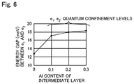
- FIG. 6 is a graph illustrating the relationship between the Al content of the intermediate layer and the energy gap between a conduction band first excitation level e 1 and a conduction band second excitation level e 2 ;
- FIGS. 7A and 7B are graphs illustrating the absorption spectra
- FIG. 8 is a graph illustrating the relationship between the Al content of the intermediate layer and the energy gap between a conduction band first excitation level e 1 and a conduction band second excitation level e 2 ;
- FIGS. 9A and 9B are graphs illustrating the absorption spectra.
- quantum dot layer refers to a layer including quantum dots, a wetting layer, an intermediate layer, an underlayer for the quantum dots, a partial capping layer for the quantum dots, an insertion layer, and the like.
- quantum dot refers to a semiconductor fine particle that has a particle size of 100 nm or less and is covered with a semiconductor material having a larger bandgap than the semiconductor material constituting the quantum dot.
- S-K Stranski-Krastanov
- underlayer for the quantum dots refers to an underlayer for growing quantum dots and a wetting layer.
- the underlayer is formed of a semiconductor material having a larger band gap than the semiconductor material constituting the quantum dots.
- partial capping layer for the quantum dots refers to a layer grown on the quantum dots.
- the partial capping layer is formed of a semiconductor material having a larger bandgap than the semiconductor material constituting the quantum dots and at least partially covers the quantum dots.
- the partial capping layer is flat.
- the partial capping layer may be shaped in conformance with the shape of the quantum dots.
- the partial capping layer has a thickness larger than or equal to the height of the quantum dots. The thickness may be smaller than or equal to the height of the quantum dots.
- intermediate layer refers to a layer serving as a matrix of the quantum dot layer and formed of a semiconductor material having a larger bandgap than the semiconductor material constituting the quantum dots.
- the intermediate layer may be formed of the same semiconductor material as the underlayer for the quantum dots and the partial capping layer for the quantum dots.
- FIG. 1 is a sectional view of a quantum dot infrared detector according to an embodiment of the present disclosure.
- a quantum dot infrared detector 10 according to an embodiment of the present disclosure includes a semiconductor substrate 1 , a buffer layer 2 , n-type semiconductor layers 3 and 5 , a photoelectric conversion layer 4 , and electrodes 6 to 8 .
- the buffer layer 2 is disposed on the semiconductor substrate 1 and in contact with one surface of the semiconductor substrate 1 .
- the n-type semiconductor layer 3 is disposed on the buffer layer 2 and in contact with the buffer layer 2 .
- the photoelectric conversion layer 4 is disposed on the n-type semiconductor layer 3 and in contact with the n-type semiconductor layer 3 .
- the n-type semiconductor layer 5 is disposed on the photoelectric conversion layer 4 and in contact with the photoelectric conversion layer 4 .
- the electrodes 6 and 7 are distant from each other and disposed on the n-type semiconductor layer 5 and in contact with the n-type semiconductor layer 5 .
- the electrode 8 is disposed on the n-type semiconductor layer 3 and in contact with the n-type semiconductor layer 3 .
- the semiconductor substrate 1 is formed of, for example, semi-insulating GaAs.
- the buffer layer 2 is formed of, for example, GaAs.
- the buffer layer 2 has a thickness of, for example, 100 nm to 500 nm.
- the n-type semiconductor layers 3 and 5 are each formed of, for example, n-GaAs.
- the n-type semiconductor layers 3 and 5 each have a thickness of, for example, 100 nm to 1000 nm.
- the electrodes 6 to 8 are n-type electrodes and formed of, for example, any one of Au/AuGeNi, AuGe/Ni/Au, Au/Ge, and Au/Ge/Ni/Au.
- the electrodes 6 to 8 each have a thickness of, for example, 10 nm to 500 nm.
- the photoelectric conversion layer 4 has a stacked structure in which quantum dot layers 41 are stacked on top of one another.
- FIG. 1 depicts the case where three quantum dot layers 41 are stacked on top of one another.
- two or more quantum dot layers 41 are stacked on top of one another.
- the quantum dot layers 41 each include quantum dots 411 , an underlayer 412 for the quantum dots 411 , a wetting layer 413 for the quantum dots 411 , a partial capping layer 414 for the quantum dots 411 , and an intermediate layer 415 .
- the underlayer 412 is disposed under the quantum dots 411 .
- the wetting layer 413 is disposed on the underlayer 412 and in contact with the underlayer 412 .
- the intermediate layer 415 is disposed on each side of a group including the quantum dots 411 , the underlayer 412 , and the wetting layer 413 .
- the quantum dot layer 41 may include an insertion layer and the like in addition to the quantum dots 411 , the underlayer 412 for the quantum dots, the wetting layer 413 , the partial capping layer 414 for the quantum dots 411 , and the intermediate layer 415 .
- the quantum dot layer 41 typically includes at least the quantum dots 411 , the underlayer 412 for the quantum dots 411 , the partial capping layer 414 for the quantum dots 411 , and the intermediate layer 415 .
- the material of the quantum dot layers 41 is not limited and may be a group III-V compound semiconductor.
- the quantum dots 411 may be formed of a semiconductor material having a smaller bandgap energy than that of the intermediate layer 415 .
- the material of the quantum dot layers 41 may be for example, any one of GaAs x Sb 1-x , AlSb, InAs x Sb 1-x , Ga x In 1-x Sb, AiSb x As 1-x , AlAs z Sb 1-z , In x Ga 1-x As, Al x Ga 1-x As, Al y Ga 1-y As z Sb 1-z , In x Ga 1-x P, (Al y Ga 1-y ) z In 1-z P, GaAs x P 1-x , Ga y In 1-y As z P 1-z , and In x Al 1-x As (in these materials, 0 ⁇ x ⁇ 1, 0 ⁇ y ⁇ 1, and 0 ⁇ z ⁇ 1, the same applies to the following description) or may be a mixed crystal material thereof.
- the material of the quantum dot layers 41 may be a compound semiconductor composed of a group IV semiconductor or a group III semiconductor material and a group V semiconductor material, or a compound semiconductor composed of a group II semiconductor material and a group VI semiconductor material, or may be a mixed crystal material thereof. These groups are listed in the periodic table.
- the material of the quantum dot layers 41 may be a chalcopyrite-based material or may be a semiconductor other than chalcopyrite-based materials.
- the photoelectric conversion layer 4 may be an i-type semiconductor layer or may be a semiconductor layer containing a p-type impurity or an n-type impurity.
- the photoelectric conversion layer 4 has a quantum dot-stacked structure.
- the quantum dot-stacked structure includes at least the quantum dots 411 , the underlayer 412 for the quantum dots 411 , the partial capping layer 414 for the quantum dots 411 , and the intermediate layer 415 .
- the quantum dots 411 , the underlayer 412 , the partial capping layer 414 , and the intermediate layer 415 are formed of, for example, the following materials.
- the quantum dots 411 are formed of InAs.
- the underlayer 412 (also referred to as a “barrier layer”. The same applies to the following description) is formed of Al 0.4 Ga 0.6 As.
- the partial capping layer 414 (also referred to as a “barrier layer”. The same applies to the following description) is formed of Al 0.4 Ga 0.6 As.
- the intermediate layer 415 is formed of GaAs.
- the underlayer 412 and the partial capping layer 414 have a thickness that allows for electron tunneling.
- the intermediate layer 415 is formed of a material having a conduction band bottom located near a conduction band first excitation level and a conduction band second excitation level, which are formed in the quantum dots 411 .
- the partial capping layer 414 is not limited to Al 0.4 Ga 0.6 As, and the partial capping layer 414 is normally formed of Al x Ga 1-x As (0 ⁇ x ⁇ 1).
- the partial capping layer 414 (barrier layer) is formed of AlGaAs, it is easy to form, on the GaAs substrate, the partial capping layer 414 (barrier layer) having a larger band gap than GaAs.
- the partial capping layer 414 (barrier layer) may be formed of InGaP or GaAsP.
- the intermediate layer 415 is a thick layer, crystal quality is taken into consideration. In the case of the AlGaAs layer, the crystal quality increases with decreasing Al content. The crystal quality of the intermediate layer 415 can thus be improved by using GaAs as a material of the intermediate layer 415 .
- FIGS. 2A and 2B are sectional views of other structures of the quantum dot layer 41 illustrated in FIG. 1 .
- the quantum dot layer 41 in an embodiment of the present disclosure may be a quantum dot layer 41 A illustrated in FIG. 2A or may be a quantum dot layer 41 B illustrated in FIG. 2B .
- the quantum dot layer 41 A is similar to the quantum dot layer 41 except that the partial capping layer 414 of the quantum dot layer 41 illustrated in FIG. 1 is replaced by the partial capping layer 414 A.
- the partial capping layer 414 A is disposed on the quantum dots 411 and the wetting layer 413 and shaped in conformance with the shape of the quantum dots 411 .
- the quantum dot layer 41 B is similar to the quantum dot layer 41 except that the partial capping layer 414 of the quantum dot layer 41 illustrated in FIG. 1 is replaced by the partial capping layer 414 B.
- the partial capping layer 414 B has the same thickness as the quantum dots 411 and is disposed on the quantum dots 411 and the wetting layer 413 .
- the partial capping layer may be any one of the partial capping layer 414 illustrated in FIG. 1 and the partial capping layers 414 A and 414 B illustrated in FIG. 2 .
- FIGS. 3A to 3E are views of a first process in a method for producing the quantum dot infrared detector 10 illustrated in FIG. 1 .
- FIGS. 4F and 4G are views of a second process in the method for producing the quantum dot infrared detector 10 illustrated in FIG. 1 .
- step (a) to step (g) illustrated in FIGS. 3A to 4G illustrate a single process including the first and second processes.
- the production of the quantum dot infrared detector 10 starts with the support of a semiconductor substrate 1 formed of semi-insulating GaAs in a molecular beam epitaxy (MBE) apparatus (step (a) in FIG. 3A ).
- MBE molecular beam epitaxy
- a buffer layer 2 is then formed on the semiconductor substrate 1 by using MBE (step (b) in FIG. 3B ).
- a GaAs layer 200 nm thick is formed as the buffer layer 2 .
- the formation of the buffer layer 2 can improve the crystallinity of a photoelectric conversion layer 4 to be formed above the buffer layer 2 . As a result, an infrared detector in which the photoelectric conversion layer 4 has high light receiving efficiency can be provided.
- an n-type semiconductor layer 3 is formed on the buffer layer 2 by using MBE (step (c) in FIG. 3C ).
- an n-GaAs layer of 500 nm is formed as the n-type semiconductor layer 3 .
- a quantum dot layer 41 including quantum dots 411 and an intermediate layer 415 is formed on the n-type semiconductor layer 3 by using MBE (step (d) in FIG. 3D ).
- the quantum dots 411 are formed by a method called Stranski-Krastanov (S-K) growth.
- a GaAs layer is crystal-grown as the intermediate layer 415 , and an Al 0.4 Ga 0.6 As layer is then crystal-grown as an underlayer 412 (barrier layer) for the quantum dots 411 .
- the quantum dots 411 made of InAs are formed through a self-assembly mechanism.
- An Al 0.4 Ga 0.6 As layer is then crystal-grown as a partial capping layer 414 so that the quantum dots 411 are embedded in the partial capping layer 414 .
- a GaAs layer is then crystal-grown as the intermediate layer to form the quantum dot layer 41 .
- step (d) is then repeated, for example, 10 times to form, on the n-type semiconductor layer 3 , the photoelectric conversion layer 4 having a structure in which the quantum dot layers 41 are stacked on top of one another (step (e) in FIG. 3E ).
- the intermediate layer 415 is much thicker than the barrier layers (the underlayer 412 and the partial capping layer 414 ) and is, for example, 40 nm thick.
- the barrier layers (the underlayer 412 and the partial capping layer 414 ) may be thin in order that excited carriers tunnel into the intermediate layer 415 .
- the barrier layers are, for example, 1 nm thick.
- the n-type semiconductor layer 5 is formed on the photoelectric conversion layer 4 by using MBE (step (f) in FIG. 4F ).
- MBE step (f) in FIG. 4F .
- an n-GaAs layer 200 nm thick is crystal-grown as the n-type semiconductor layer 5 .
- a nin structure is formed.
- the multilayer sample is taken out of the MBE apparatus, and the photoelectric conversion layer 4 and the n-type semiconductor layer 5 are partially removed by using photolithography and wet etching. Electrodes 6 and 7 are formed on the n-type semiconductor layer 5 , and an electrode 8 is formed on the n-type semiconductor layer 3 .
- a quantum dot infrared detector 10 is completed accordingly (step (g) in FIG. 4G ).
- Si can be used as an n-type dopant.
- Au may be used for the electrodes 6 to 8 , and the electrodes 6 to 8 may be formed by vacuum deposition using resistance-heating vacuum deposition.
- Using AlGaAs in the underlayer 412 and the partial capping layer 414 for the quantum dots 411 can improve the surface flatness of the underlayer 412 and the partial capping layer 414 while providing the quantum confinement effect of the quantum dots, and can provide the quantum dot infrared detector 10 that includes a large number of the quantum dot layers 41 but in which dislocations or the like are unlikely to occur.
- the transition between the conduction band ground level e 0 and the conduction band first excitation level e 1 (and the conduction band second excitation level e 2 ) exhibits strong absorption of light polarized in the direction perpendicular to the stacking direction of the quantum dot layers 41 .
- the photocurrent in the polarization direction perpendicular to the stacking direction is greater than the photocurrent in the polarization direction corresponding to the stacking direction. This is because light polarized in the in-plane direction is strongly absorbed due to the conduction band first excitation level e 1 and the conduction band second excitation level e 2 being quantum levels strongly affected by the size in the in-plane direction.
- the photocurrent in the polarization direction perpendicular to the stacking direction of the quantum dot layers 41 can be compared with the photocurrent in the polarization direction corresponding to the stacking direction as follows: for example, polishing the substrate end surface of a sample such that the substrate end surface forms an angle of 45 degrees with respect to the stacking direction and causing light to strike the substrate end surface through a polarizing plate. More specifically, the photocurrent in the polarization direction perpendicular to the stacking direction of the quantum dot layers 41 is compared with the photocurrent in the polarization direction at 45 degrees with respect to the stacking direction.
- the photocurrent in the polarization direction perpendicular to the stacking direction is greater than the photocurrent in the polarization direction corresponding to the stacking direction
- the photocurrent in the polarization direction perpendicular to the stacking direction will be greater than the photocurrent in the polarization direction at 45 degrees with respect to the stacking direction.
- the surface incidence in an infrared detector normally results in a large drop in sensitivity.
- FIGS. 5A and 5B are schematic diagrams illustrating the energy levels of the quantum dots 411 , the barrier layers (the underlayer 412 and the partial capping layer 414 ), and the intermediate layer 415 in the quantum dot layer 41 .
- FIG. 5A depicts the energy levels of quantum dots, a barrier layer, and an intermediate layer in an existing quantum dot layer.
- FIG. 5B depicts the energy levels of the quantum dots 411 , the barrier layers (the underlayer 412 and the partial capping layer 414 ), and the intermediate layer 415 in the quantum dot layer 41 according to the embodiment of the present disclosure.
- the conduction band first excitation level e 1 and the conduction band second excitation level e 2 are discrete and form quantum confinement levels (see FIG. 5A ).
- discrete means that the energy gap is greater than thermal energy.
- the conduction band first excitation level e 1 and the conduction band second excitation level e 2 are not discrete levels. This is because the conduction band first excitation level e 1 and the conduction band second excitation level e 2 are located near the conduction band bottom of the intermediate layer 415 .
- the expression “the energy gap E GAP3-2 is much smaller than an LO phonon energy of 36 meV” means that, for example, the energy gap E GAP3-2 is much smaller than thermal energy (26 meV at room temperature).
- the conduction band first excitation level e 1 and the conduction band second excitation level e 2 form continuous-like states with the conduction band of the intermediate layer 415 .
- continuous-like states means the states in which the conduction band first excitation level e 1 and the conduction band second excitation level e 2 interact with the continuous states of the conduction band of the intermediate layer 415 ; that is, the states in which the electron wave functions in the conduction band first excitation level e 1 and the conduction band second excitation level e 2 are present in both the quantum dots 411 and the conduction band of the intermediate layer 415 .
- the continuous-like states are achieved by forming the intermediate layer 415 using a material having the conduction band bottom of the intermediate layer 415 located near the conduction band first excitation level e 1 and the conduction band second excitation level e 2 and setting the thickness of the barrier layers (the underlayer 412 and the partial capping layer 414 ) to a thickness that allows for electron tunneling.
- the continuous-like states are achieved even without the barrier layers (the underlayer 412 and the partial capping layer 414 ) as long as the intermediate layer 415 is formed of a material having the conduction band bottom of the intermediate layer 415 located near the conduction band first excitation level e 1 and the conduction band second excitation level e 2 .
- the quantum confinement levels include the conduction band ground level e 0 , the conduction band first excitation level e 1 , and the conduction band second excitation level e 2 , which are formed in the quantum dots.
- the conduction band first excitation level e 1 and the conduction band second excitation level e 2 do not form continuous-like states with the conduction band of the intermediate layer.
- the quantum confinement levels of the quantum dot layer 41 include only the conduction band ground level e 0 among the conduction band ground level e 0 , the conduction band first excitation level e 1 , and the conduction band second excitation level e 2 , which are formed in the quantum dots 411 .
- the conduction band first excitation level e 1 and the conduction band second excitation level e 2 form continuous-like states with the conduction band of the intermediate layer 415 .
- the quantum dot layer 41 completely differs from an existing quantum dot layer.
- the conduction band first excitation level e 1 and the conduction band second excitation level e 2 form continuous-like states with the conduction band of the intermediate layer 415 .
- the emission peaks include a separated single peak from the conduction band ground level e 0 and a peak group including overlapped and successive peaks composed of a peak from the conduction band first excitation level e 1 , a peak from the conduction band second excitation level e 2 , and a peak from the conduction band of the intermediate layer 415 .
- the emission peaks include a separated single peak from the conduction band ground level e 0 and a peak group including successive peaks from the conduction band first excitation level e 1 , the conduction band second excitation level e 2 , and the conduction band of the intermediate layer 415 that form continuous states.
- the absorption band half-width is not broad. This leads to high wavelength selectivity for photodetection.
- Whether the conduction band first excitation level e 1 and the conduction band second excitation level e 2 form continuous-like states with the conduction band of the intermediate layer 415 is determined based on the emission characteristics of the quantum dot infrared detector 10 . More specifically, in the case where the quantum confinement levels include only the conduction band ground level e 0 (see FIG. 5B ), a separated single peak and a peak group including successively connected peaks appear. In the case where the quantum confinement levels include the conduction band first excitation level e 1 and the conduction band second excitation level e 2 (see FIG. 5A ), a plurality of separated single peaks appears.
- the conduction band first excitation level e 1 and the conduction band second excitation level e 2 do not form continuous-like states with the conduction band of the intermediate layer 415 .
- the term “separated single peak” means that the energy gap between the single peak and an adjacent peak is much larger than thermal energy; that is, the single peak is not continuous with an adjacent peak.
- the states in which the conduction band first excitation level e 1 and the conduction band second excitation level e 2 form continuous-like states with the conduction band of the intermediate layer 415 may be the states in which the emission peaks associated with the conduction band first excitation level e 1 or greater levels are continuous with that associated with the conduction band of the intermediate layer 415 and the emission peak associated with the conduction band ground level e 0 is distant from that associated with the conduction band by thermal energy or greater.
- the continuous-like states are achieved by realizing any one of the following (A), (B), and (C).
- the energy gap between the conduction band first excitation level e 1 and the conduction band bottom of the intermediate layer 415 and the energy gap between the conduction band second excitation level e 2 and the conduction band bottom of the intermediate layer 415 are each smaller than twice thermal energy.
- the energy gap between the conduction band second excitation level e 2 and the conduction band third excitation level e 3 is smaller than thermal energy.
- the emission spectrum detected as a result of incidence of an electromagnetic wave on or injection of a current into the quantum dot infrared detector 10 includes a separated single peak and a peak group including successive peaks. The energy gap between the separated single peak and the peak group is larger than thermal energy. The energy gap between the peaks in the peak group is smaller than thermal energy.
- continuous-like states are used for an easy understanding of the quantum dot infrared detector 10 according to the embodiment of the present disclosure. It is understood that the term “continuous-like states” are not used to determine the scope of the present disclosure. The scope of the present disclosure is determined based on the description of the claims, at which time the scope of the present disclosure is not determined in light of the meaning and context of the term “continuous-like states”.
- the structure of the quantum dot infrared detector 10 can be determined based on the emission spectra. Moreover, the structure of the quantum dot infrared detector 10 can be determined by analyzing the band structure based on the numerical calculations using the shape and composition of the quantum dots in the quantum dot structure and the thickness and composition of the underlayer for the quantum dots, the partial capping layer for the quantum dots, and the insertion layer.
- a quantum dot infrared detector is produced in accordance with step (a) to step (g) illustrated in FIGS. 3A to 3E and FIGS. 4F and 4G .
- Al x Ga 1-x As is used as a material of the intermediate layer 415 , and x is varied in the range from 0 to 0.3.
- FIG. 6 is a graph illustrating the relationship between the Al content of the intermediate layer 415 and the energy gap between the conduction band first excitation level e 1 and the conduction band second excitation level e 2 .
- the vertical axis represents the energy gap between the conduction band first excitation level e 1 and the conduction band second excitation level e 2
- the horizontal axis represents the Al content of the intermediate layer 415 .
- the results in FIG. 6 are calculation results, and the calculation conditions are as described below.
- the quantum dots 411 and the wetting layer 413 are formed of InAs.
- the barrier layers (the underlayer 412 and the partial capping layer 414 ) are formed of Al 0.4 Ga 0.6 As.
- the quantum dot 411 has a pyramid shape. In consideration of 10% in-plane size anisotropy, the size in the [110] direction is 18 nm, and the size in the [1-10] direction is 10% larger than that in the [110] direction.
- the height of the quantum dots 411 is 4 nm.
- the thickness of the wetting layer 413 is 0.5 nm, and the thickness of the barrier layers (the underlayer 412 and the partial capping layer 414 ) is 1 nm.
- the calculation method uses a single band.
- the energy gap E GAP1-2 between the conduction band first excitation level e 1 and the conduction band second excitation level e 2 is the smallest when the Al content of the intermediate layer 415 is “0”.
- the energy gap E GAP1-2 increases as the Al content of the intermediate layer 415 increases.
- the energy positions of the conduction band first excitation level e 1 and the conduction band second excitation level e 2 are located near the conduction band bottom of the intermediate layer 415 .
- the conduction band first excitation level e 1 and the conduction band second excitation level e 2 are less discretized, and the energy gap E GAP1-2 between the conduction band first excitation level e 1 and the conduction band second excitation level e 2 is small. Therefore, the conduction band first excitation level e 1 and the conduction band second excitation level e 2 are in continuous states, which improves wavelength selectivity for photodetection.
- Whether the conduction band first excitation level e 1 and the conduction band second excitation level e 2 form discrete quantum confinement levels is determined based on the energy gap E GAP2-3 between the conduction band second excitation level e 2 and the conduction band third excitation level e 3 .
- the conduction band first excitation level e 1 and the conduction band second excitation level e 2 form discrete quantum confinement levels (see FIG. 5A ).
- the conduction band first excitation level e 1 and the conduction band second excitation level e 2 are not discrete levels (see FIG. 5B ). This is because the energy positions of the conduction band first excitation level e 1 and the conduction band second excitation level e 2 are located near the conduction band bottom of the intermediate layer 415 .
- the energy gap E GAP2-3 is 78 meV, which is much larger than an LO phonon energy of 36 meV.
- the conduction band first excitation level e 1 and the conduction band second excitation level e 2 form discrete quantum confinement levels (see FIG. 5A ).
- the energy gap E GAP2-3 is 76 meV, which is much larger than an LO phonon energy of 36 meV.
- the conduction band first excitation level e 1 and the conduction band second excitation level e 2 form discrete quantum confinement levels (see FIG. 5A ).
- the energy gap E GAP2-3 is 70 meV, which is much larger than an LO phonon energy of 36 meV.
- the conduction band first excitation level e 1 and the conduction band second excitation level e 2 form discrete quantum confinement levels (see FIG. 5A ).
- the energy gap E GAP2-3 is 8 meV, which is much smaller than an LO phonon energy of 36 meV.
- the conduction band first excitation level e 1 and the conduction band second excitation level e 2 are not discrete levels (see FIG. 5B ).
- the conduction band first excitation level e 1 and the conduction band second excitation level e 2 form discrete quantum confinement levels.
- the conduction band first excitation level e 1 and the conduction band second excitation level e 2 are not discrete levels.
- a quantum dot infrared detector in which the Al content x of the intermediate layer 415 is 0 is defined as a quantum dot infrared detector of Example 1.
- Quantum dot infrared detectors in which the Al content x of the intermediate layer 415 is 0.1, 0.2, and 0.3 are defined as quantum dot infrared detectors of Comparative Examples 1, 2, and 3, respectively.
- FIGS. 7A and 7B are graphs illustrating the absorption spectra.
- the vertical axis represents absorption coefficient and the horizontal axis represents energy.
- the curve k1 indicates the absorption spectrum in the [1-10] polarization direction (the same direction as the crystal axis of the quantum dot 411 ).
- the curve k2 indicates the absorption spectrum in the [110]polarization direction.
- the curve k3 indicates the sum of these two absorption spectra.
- the curve k4 indicates the absorption spectrum in the [1-10] polarization direction (the same direction as the crystal axis of the quantum dot 411 ).
- the curve k5 indicates the absorption spectrum in the [110] polarization direction.
- the curve k6 indicates the sum of these two absorption spectra.
- the absorption peaks of polarized light are observed at 115 meV (10.8 ⁇ m) and 133 meV (9.3 ⁇ m), and the energy gap between the absorption peaks is 18 meV.
- the energy gap of 18 meV corresponds to the energy gap E GAP1-2 between the conduction band first excitation level e 1 and the conduction band second excitation level e 2 when the Al content of the intermediate layer 415 is 0.2 in FIG. 6 .
- Example 1 in Example 1 where the Al content x of the intermediate layer 415 is 0, the absorption peaks of polarized light are observed at 103 meV (12.0 ⁇ m) and 116 meV (10.7 ⁇ m), and the energy gap between the absorption peaks is 13 meV.
- the energy gap of 13 meV corresponds to the energy gap E GAP1-2 between the conduction band first excitation level e 1 and the conduction band second excitation level e 2 when the Al content of the intermediate layer 415 is 0 in FIG. 6 .
- the half-width of the detection band in FIG. 7B is reduced to about 30 meV from about 36 meV in FIG. 7A .
- the quantum dot infrared detector of Example 1 has a narrower half-width of the detection band than the quantum dot infrared detector of Comparative Example 2.
- FIG. 8 is a graph illustrating the relationship between the Al content of the intermediate layer 415 and the energy gap between a conduction band first excitation level e 1 and a conduction band second excitation level e 2 .
- the vertical axis represents the energy gap between the conduction band first excitation level e 1 and the conduction band second excitation level e 2
- the horizontal axis represents the Al content of the intermediate layer 415 .
- the calculation results depicted in FIG. 8 are obtained by calculation using the same calculation conditions as those in Example 1 except that, regarding the in-plane size anisotropy of the quantum dots 411 , the size in the [1-10] direction is 15% larger than that in the [110] direction.
- the energy gap E GAP1-2 between the conduction band first excitation level e 1 and the conduction band second excitation level e 2 has substantially the same relationship with the Al content of the intermediate layer 415 as in Example 1.
- Example 1 when the Al content of the intermediate layer 415 varies from 0.3 to 0, a change in the energy gap E GAP1-2 between the conduction band first excitation level e 1 and the conduction band second excitation level e 2 is 5 meV. When the Al content of the intermediate layer 415 varies from 0.1 to 0, a change in the energy gap E GAP1-2 between the conduction band first excitation level e 1 and the conduction band second excitation level e 2 is 4 meV.
- Example 2 when the Al content of the intermediate layer 415 varies from 0.3 to 0, a change in the energy gap E GAP1-2 between the conduction band first excitation level e 1 and the conduction band second excitation level e 2 is 7 meV. When the Al content of the intermediate layer 415 varies from 0.1 to 0, a change in the energy gap E GAP1-2 between the conduction band first excitation level e 1 and the conduction band second excitation level e 2 is 5 meV.
- Example 2 whether the conduction band first excitation level e 1 and the conduction band second excitation level e 2 form discrete quantum confinement levels is also determined based on the energy gap E GAP2-3 between the conduction band second excitation level e 2 and the conduction band third excitation level e 3 .
- the energy gap E GAP2-3 is 67 meV, which is much larger than an LO phonon energy of 36 meV.
- the conduction band first excitation level e 1 and the conduction band second excitation level e 2 form discrete quantum confinement levels (see FIG. 5A ).
- the energy gap E PAP2-3 is 72 meV, which is much larger than an LO phonon energy of 36 meV.
- the conduction band first excitation level e 1 and the conduction band second excitation level e 2 form discrete quantum confinement levels (see FIG. 5A ).
- the energy gap E GAP2-3 is 75 meV, which is much larger than an LO phonon energy of 36 meV.
- the conduction band first excitation level e 1 and the conduction band second excitation level e 2 form discrete quantum confinement levels (see FIG. 5A ).
- the energy gap E GAP2-3 is 9 meV, which is much smaller than an LO phonon energy of 36 meV.
- the conduction band first excitation level e 1 and the conduction band second excitation level e 2 are not discrete levels (see FIG. 5B ).
- the conduction band first excitation level e 1 and the conduction band second excitation level e 2 form discrete quantum confinement levels.
- the conduction band first excitation level e 1 and the conduction band second excitation level e 2 are not discrete levels.
- a quantum dot infrared detector in which the Al content x of the intermediate layer 415 is 0 is defined as a quantum dot infrared detector of Example 2.
- Quantum dot infrared detectors in which the Al content x of the intermediate layer 415 is 0.1, 0.2, and 0.3 are defined as quantum dot infrared detectors of Comparative Examples 4, 5, and 6, respectively.
- the quantum dot infrared detector of Example 2 is produced in the same manner as the quantum dot infrared detector of Example 1 except that the percentage of in-plane size anisotropy of the quantum dot 411 is changed to 15%, that is, the size in the [110] direction is 18 nm, and the size in the [1-10] direction is 15% larger than that in the [110] direction.
- the quantum dot infrared detectors of Comparative Examples 4, 5, and 6 are produced in the same manner as the quantum dot infrared detectors of Comparative Examples 1, 2, and 3 except that the size in the [110] direction is 18 nm, and the size in the [1-10] direction is 15% larger than that in the [110] direction.
- FIGS. 9A and 9B are graphs illustrating the absorption spectra.
- the vertical axis represents absorption coefficient and the horizontal axis represents energy.
- the curve k7 indicates the absorption spectrum in the [1-10] polarization direction (the same direction as the crystal axis of the quantum dot 411 ).
- the curve k8 indicates the absorption spectrum in the [110] polarization direction.
- the curve k9 indicates the sum of these two absorption spectra.
- the curve k10 indicates the absorption spectrum in the [1-10] polarization direction (the same direction as the crystal axis of the quantum dot 411 ).
- the curve k11 indicates the absorption spectrum in the [110] polarization direction.
- the curve k12 indicates the sum of these two absorption spectra.
- the absorption peaks of polarized light are observed at 110 meV (11.2 ⁇ m) and 133 meV (9.3 ⁇ m), and the energy gap between the absorption peaks is 23 meV.
- the energy gap of 23 meV corresponds to the energy gap E GAP1-2 between the conduction band first excitation level e 1 and the conduction band second excitation level e 2 when the Al content of the intermediate layer 415 is 0.2 in FIG. 8 .
- the absorption peaks of polarized light are observed at 100 meV (12.3 ⁇ m) and 117 meV (10.5 ⁇ m), and the energy gap between the absorption peaks is 17 meV.
- the energy gap of 17 meV corresponds to the energy gap E GAP1-2 between the conduction band first excitation level e 1 and the conduction band second excitation level e 2 when the Al content of the intermediate layer 415 is 0 in FIG. 8 .
- the half-width of the detection band in FIG. 9B is reduced to about 35 meV from about 46 meV in FIG. 9 A.
- the quantum dot infrared detector of Comparative Example 2 has a narrower half-width of the detection band than the quantum dot infrared detector of Comparative Example 5.
- the conduction band first excitation level e 1 and the conduction band second excitation level e 2 form continuous-like states with the conduction band of the intermediate layer 415 , and the quantum confinement levels include only the conduction band ground level e 0 .
- the conduction band first excitation level e 1 and the conduction band second excitation level e 2 are discrete levels.
- the quantum dot infrared detector of Example 2 has a narrower half-width of the detection band than the quantum dot infrared detectors of Comparative Examples 4, 5, and 6.
- a quantum dot infrared detector includes a quantum dot-stacked structure that includes quantum dot layers stacked on top of one another and each including quantum dots and an intermediate layer.
- the quantum dots have conduction band quantum confinement levels that include a conduction band ground level, a conduction band first excitation level at a higher energy position than the conduction band ground level, and a conduction band second excitation level at a higher energy position than the conduction band ground level.
- An energy gap between the conduction band first excitation level and a conduction band bottom of the intermediate layer and an energy gap between the conduction band second excitation level and the conduction band bottom of the intermediate layer are each smaller than twice thermal energy.
- the conduction band ground level and the conduction band first excitation level are discrete levels.
- the energy gap between the conduction band first excitation level and the conduction band bottom of the intermediate layer and the energy gap between the conduction band second excitation level and the conduction band bottom of the intermediate layer are each smaller than twice thermal energy, the continuous-like states are achieved, and the half-width for photodetection in the 8-14 ⁇ m band can be reduced.
- a quantum dot infrared detector includes a quantum dot-stacked structure in which quantum dot layers containing quantum dots are stacked on top of one another.
- the quantum dots have conduction band quantum confinement levels that include a conduction band ground level, and a conduction band first excitation level, a conduction band second excitation level, and a conduction band third excitation level each at a higher energy position than the conduction band ground level.
- An energy gap between the conduction band second excitation level and the conduction band third excitation level is smaller than thermal energy.
- the conduction band ground level and the conduction band first excitation level are discrete levels.
- the energy gap between the conduction band second excitation level and the conduction band third excitation level is smaller than thermal energy, the continuous-like states are achieved, and the half-width for photodetection in the 8-14 ⁇ m band can be reduced.
- a quantum dot infrared detector includes a quantum dot-stacked structure that includes quantum dot layers stacked on top of one another and each including quantum dots.
- the quantum dots have conduction band quantum confinement levels that include a conduction band ground level and a conduction band first excitation level at a higher energy level than the conduction band ground level.
- the conduction band ground level and the conduction band first excitation level are discrete levels.
- An emission spectrum detected as a result of incidence of an electromagnetic wave on or injection of a current into the quantum dot infrared detector includes a separated single peak and a peak group including successive peaks; an energy gap between the separated single peak and the peak group is larger than thermal energy; and an energy gap between the peaks in the peak group is smaller than thermal energy.
- the energy gap between the separated single peak and the peak group is larger than thermal energy and the energy gap between the peaks in the peak group is smaller than thermal energy, the continuous-like states are achieved, and the half-width for photodetection in the 8-14 ⁇ m band can be reduced.
- the present disclosure is applied to quantum dot infrared detectors.
Landscapes
- Light Receiving Elements (AREA)
- Physics & Mathematics (AREA)
- Spectroscopy & Molecular Physics (AREA)
- Chemical & Material Sciences (AREA)
- Engineering & Computer Science (AREA)
- Nanotechnology (AREA)
Abstract
Description
(B) The energy gap between the conduction band second excitation level e2 and the conduction band third excitation level e3 is smaller than thermal energy.
(C) The emission spectrum detected as a result of incidence of an electromagnetic wave on or injection of a current into the quantum dot
Claims (6)
Applications Claiming Priority (2)
| Application Number | Priority Date | Filing Date | Title |
|---|---|---|---|
| JP2017-169697 | 2017-09-04 | ||
| JP2017169697A JP6660358B2 (en) | 2017-09-04 | 2017-09-04 | Quantum dot type infrared detector |
Publications (2)
| Publication Number | Publication Date |
|---|---|
| US20190074320A1 US20190074320A1 (en) | 2019-03-07 |
| US10636833B2 true US10636833B2 (en) | 2020-04-28 |
Family
ID=63490353
Family Applications (1)
| Application Number | Title | Priority Date | Filing Date |
|---|---|---|---|
| US16/120,798 Expired - Fee Related US10636833B2 (en) | 2017-09-04 | 2018-09-04 | Quantum dot infrared detector |
Country Status (3)
| Country | Link |
|---|---|
| US (1) | US10636833B2 (en) |
| EP (1) | EP3451391A1 (en) |
| JP (1) | JP6660358B2 (en) |
Families Citing this family (1)
| Publication number | Priority date | Publication date | Assignee | Title |
|---|---|---|---|---|
| CN111739963B (en) * | 2020-06-10 | 2022-07-22 | 中国科学院上海微系统与信息技术研究所 | A kind of preparation method of silicon-based wide-spectrum photodetector |
Citations (6)
| Publication number | Priority date | Publication date | Assignee | Title |
|---|---|---|---|---|
| US20010028055A1 (en) | 1998-05-05 | 2001-10-11 | Simon Fafard | Quantum dot infrared photodetector (QDIP) and methods of making the same |
| US20100032552A1 (en) * | 2008-08-08 | 2010-02-11 | Technical Research & Development Institute Ministry Of Defense Of Japan | Optical semiconductor device |
| US20100032652A1 (en) | 2008-08-08 | 2010-02-11 | Technical Research & Development Institute Ministry Of Defense Of Japan | Infrared photodetector |
| WO2011050165A2 (en) | 2009-10-21 | 2011-04-28 | Stc.Unm | Plasmonic detectors |
| US20120285537A1 (en) * | 2011-05-09 | 2012-11-15 | Sharp Kabushiki Kaisha | Solar cell |
| JP2016136585A (en) | 2015-01-23 | 2016-07-28 | 防衛装備庁長官 | Method of manufacturing infrared ray detector |
Family Cites Families (1)
| Publication number | Priority date | Publication date | Assignee | Title |
|---|---|---|---|---|
| JP2009065142A (en) * | 2008-08-08 | 2009-03-26 | Technical Research & Development Institute Ministry Of Defence | Quantum dot infrared detector |
-
2017
- 2017-09-04 JP JP2017169697A patent/JP6660358B2/en not_active Expired - Fee Related
-
2018
- 2018-09-03 EP EP18192297.2A patent/EP3451391A1/en not_active Withdrawn
- 2018-09-04 US US16/120,798 patent/US10636833B2/en not_active Expired - Fee Related
Patent Citations (8)
| Publication number | Priority date | Publication date | Assignee | Title |
|---|---|---|---|---|
| US20010028055A1 (en) | 1998-05-05 | 2001-10-11 | Simon Fafard | Quantum dot infrared photodetector (QDIP) and methods of making the same |
| US20100032552A1 (en) * | 2008-08-08 | 2010-02-11 | Technical Research & Development Institute Ministry Of Defense Of Japan | Optical semiconductor device |
| US20100032652A1 (en) | 2008-08-08 | 2010-02-11 | Technical Research & Development Institute Ministry Of Defense Of Japan | Infrared photodetector |
| WO2011050165A2 (en) | 2009-10-21 | 2011-04-28 | Stc.Unm | Plasmonic detectors |
| US20120205541A1 (en) | 2009-10-21 | 2012-08-16 | Seung-Chang Lee | Plasmonic detectors |
| US20120285537A1 (en) * | 2011-05-09 | 2012-11-15 | Sharp Kabushiki Kaisha | Solar cell |
| JP2016136585A (en) | 2015-01-23 | 2016-07-28 | 防衛装備庁長官 | Method of manufacturing infrared ray detector |
| JP5976141B2 (en) * | 2015-01-23 | 2016-08-23 | 防衛装備庁長官 | Infrared detector manufacturing method |
Non-Patent Citations (5)
| Title |
|---|
| Ariyawansa, G. et al., Bias-selectable tricolor tunneling quantum dot infrared photodetector for atmospheric windows, Applied Physics Letters, Mar. 19, 2008, vol. 92, pp. 111104-1-111104-3. |
| Jamie Phillips, "Evaluation of the fundamental properties of quantum dot infrared detectors", Journal of Applied Physics vol. 91, 4590 (2002). |
| Mitin et al. Nanoscale Res Lett 2011, 6:21 (Year: 2011). * |
| Mitsuhiro Nagashima et al., "Photodetection around 10 μm wavelength using s-p transitions in InAs/AIAs/AIGaAs self-assembled quantum dots", Journal of Applied Physics 107, 054504 (2010). |
| Nextnano, Dispersion in infinite superlattices: minibands, archived on Oct. 13, 2015 (https://web.archive.org/web/20151013035927/https://www.nextnano.de/nextnano3/tutorial/1Dtutorial14.htm) (Year: 2015). * |
Also Published As
| Publication number | Publication date |
|---|---|
| JP6660358B2 (en) | 2020-03-11 |
| JP2019047000A (en) | 2019-03-22 |
| EP3451391A1 (en) | 2019-03-06 |
| US20190074320A1 (en) | 2019-03-07 |
Similar Documents
| Publication | Publication Date | Title |
|---|---|---|
| US8058642B2 (en) | Light-receiving device | |
| CN105684164B (en) | Infrared-ray detecting element | |
| CN106847933A (en) | Ultraviolet infrared double color avalanche photodide of single-chip integration and preparation method thereof | |
| US20170200841A1 (en) | Photoelectric conversion element having quantum structure using indirect transition conductor material | |
| US10181539B2 (en) | Photoelectric conversion element and photoelectric conversion device including the same | |
| US20100032651A1 (en) | Quantum dot infrared photodetector | |
| US20150034153A1 (en) | Compound photovoltaic cell | |
| US20140326302A1 (en) | Solar cell | |
| US9240507B2 (en) | Intermediate band solar cell using type I and type II quantum dot superlattices | |
| US20120217475A1 (en) | Optoelectronic Devices Including Compound Valence-Band Quantum Well Structures | |
| Mensz et al. | Design and implementation of bound-to-quasibound GaN/AlGaN photovoltaic quantum well infrared photodetectors operating in the short wavelength infrared range at room temperature | |
| CN113646906A (en) | Superlattice absorbers for detectors | |
| US10636833B2 (en) | Quantum dot infrared detector | |
| JP5279070B2 (en) | Semiconductor element | |
| JP6030971B2 (en) | Light receiving element and solar cell provided with light receiving element | |
| CN113272974B (en) | Semiconductor light emitting element and method for manufacturing semiconductor light emitting element | |
| US10811554B2 (en) | Infrared photodetector | |
| CN113972292A (en) | InP-based base band gap adjustable structure and photoelectric conversion device | |
| US20180331240A1 (en) | Quantum dot infrared detector | |
| CN108538935B (en) | Tunnel-compensated superlattice infrared detector | |
| JP2011071306A (en) | Photodetector, and method of manufacturing the same | |
| JP4927911B2 (en) | Quantum dot photodetector | |
| US20180308999A1 (en) | Semiconductor light receiving device | |
| JP6312450B2 (en) | Light receiving element and solar cell provided with light receiving element | |
| JP4694417B2 (en) | Quantum dot optical semiconductor device |
Legal Events
| Date | Code | Title | Description |
|---|---|---|---|
| AS | Assignment |
Owner name: SHARP KABUSHIKI KAISHA, JAPAN Free format text: ASSIGNMENT OF ASSIGNORS INTEREST;ASSIGNORS:YOSHIKAWA, HIROFUMI;ARAKAWA, YASUHIKO;SIGNING DATES FROM 20180605 TO 20180606;REEL/FRAME:046778/0215 Owner name: THE UNIVERSITY OF TOKYO, JAPAN Free format text: ASSIGNMENT OF ASSIGNORS INTEREST;ASSIGNORS:YOSHIKAWA, HIROFUMI;ARAKAWA, YASUHIKO;SIGNING DATES FROM 20180605 TO 20180606;REEL/FRAME:046778/0215 |
|
| FEPP | Fee payment procedure |
Free format text: ENTITY STATUS SET TO UNDISCOUNTED (ORIGINAL EVENT CODE: BIG.); ENTITY STATUS OF PATENT OWNER: LARGE ENTITY |
|
| STPP | Information on status: patent application and granting procedure in general |
Free format text: DOCKETED NEW CASE - READY FOR EXAMINATION |
|
| STPP | Information on status: patent application and granting procedure in general |
Free format text: NON FINAL ACTION MAILED |
|
| STPP | Information on status: patent application and granting procedure in general |
Free format text: RESPONSE TO NON-FINAL OFFICE ACTION ENTERED AND FORWARDED TO EXAMINER |
|
| STPP | Information on status: patent application and granting procedure in general |
Free format text: NOTICE OF ALLOWANCE MAILED -- APPLICATION RECEIVED IN OFFICE OF PUBLICATIONS |
|
| STCF | Information on status: patent grant |
Free format text: PATENTED CASE |
|
| FEPP | Fee payment procedure |
Free format text: MAINTENANCE FEE REMINDER MAILED (ORIGINAL EVENT CODE: REM.); ENTITY STATUS OF PATENT OWNER: LARGE ENTITY |
|
| LAPS | Lapse for failure to pay maintenance fees |
Free format text: PATENT EXPIRED FOR FAILURE TO PAY MAINTENANCE FEES (ORIGINAL EVENT CODE: EXP.); ENTITY STATUS OF PATENT OWNER: LARGE ENTITY |
|
| STCH | Information on status: patent discontinuation |
Free format text: PATENT EXPIRED DUE TO NONPAYMENT OF MAINTENANCE FEES UNDER 37 CFR 1.362 |
|
| FP | Lapsed due to failure to pay maintenance fee |
Effective date: 20240428 |