US10636618B2 - Charged particle beam apparatus - Google Patents
Charged particle beam apparatus Download PDFInfo
- Publication number
- US10636618B2 US10636618B2 US16/115,103 US201816115103A US10636618B2 US 10636618 B2 US10636618 B2 US 10636618B2 US 201816115103 A US201816115103 A US 201816115103A US 10636618 B2 US10636618 B2 US 10636618B2
- Authority
- US
- United States
- Prior art keywords
- charged particle
- particle beam
- optical axis
- object lens
- control parameters
- Prior art date
- Legal status (The legal status is an assumption and is not a legal conclusion. Google has not performed a legal analysis and makes no representation as to the accuracy of the status listed.)
- Active
Links
Images


Classifications
-
- H—ELECTRICITY
- H01—ELECTRIC ELEMENTS
- H01J—ELECTRIC DISCHARGE TUBES OR DISCHARGE LAMPS
- H01J37/00—Discharge tubes with provision for introducing objects or material to be exposed to the discharge, e.g. for the purpose of examination or processing thereof
- H01J37/02—Details
- H01J37/04—Arrangements of electrodes and associated parts for generating or controlling the discharge, e.g. electron-optical arrangement or ion-optical arrangement
- H01J37/153—Electron-optical or ion-optical arrangements for the correction of image defects, e.g. stigmators
-
- H—ELECTRICITY
- H01—ELECTRIC ELEMENTS
- H01J—ELECTRIC DISCHARGE TUBES OR DISCHARGE LAMPS
- H01J37/00—Discharge tubes with provision for introducing objects or material to be exposed to the discharge, e.g. for the purpose of examination or processing thereof
- H01J37/02—Details
- H01J37/04—Arrangements of electrodes and associated parts for generating or controlling the discharge, e.g. electron-optical arrangement or ion-optical arrangement
- H01J37/147—Arrangements for directing or deflecting the discharge along a desired path
-
- H—ELECTRICITY
- H01—ELECTRIC ELEMENTS
- H01J—ELECTRIC DISCHARGE TUBES OR DISCHARGE LAMPS
- H01J37/00—Discharge tubes with provision for introducing objects or material to be exposed to the discharge, e.g. for the purpose of examination or processing thereof
- H01J37/02—Details
- H01J37/04—Arrangements of electrodes and associated parts for generating or controlling the discharge, e.g. electron-optical arrangement or ion-optical arrangement
- H01J37/10—Lenses
- H01J37/14—Lenses magnetic
-
- H—ELECTRICITY
- H01—ELECTRIC ELEMENTS
- H01J—ELECTRIC DISCHARGE TUBES OR DISCHARGE LAMPS
- H01J37/00—Discharge tubes with provision for introducing objects or material to be exposed to the discharge, e.g. for the purpose of examination or processing thereof
- H01J37/02—Details
- H01J37/04—Arrangements of electrodes and associated parts for generating or controlling the discharge, e.g. electron-optical arrangement or ion-optical arrangement
- H01J37/147—Arrangements for directing or deflecting the discharge along a desired path
- H01J37/1471—Arrangements for directing or deflecting the discharge along a desired path for centering, aligning or positioning of ray or beam
-
- H—ELECTRICITY
- H01—ELECTRIC ELEMENTS
- H01J—ELECTRIC DISCHARGE TUBES OR DISCHARGE LAMPS
- H01J37/00—Discharge tubes with provision for introducing objects or material to be exposed to the discharge, e.g. for the purpose of examination or processing thereof
- H01J37/02—Details
- H01J37/04—Arrangements of electrodes and associated parts for generating or controlling the discharge, e.g. electron-optical arrangement or ion-optical arrangement
- H01J37/147—Arrangements for directing or deflecting the discharge along a desired path
- H01J37/1472—Deflecting along given lines
- H01J37/1474—Scanning means
-
- H—ELECTRICITY
- H01—ELECTRIC ELEMENTS
- H01J—ELECTRIC DISCHARGE TUBES OR DISCHARGE LAMPS
- H01J37/00—Discharge tubes with provision for introducing objects or material to be exposed to the discharge, e.g. for the purpose of examination or processing thereof
- H01J37/02—Details
- H01J37/20—Means for supporting or positioning the object or the material; Means for adjusting diaphragms or lenses associated with the support
-
- H—ELECTRICITY
- H01—ELECTRIC ELEMENTS
- H01J—ELECTRIC DISCHARGE TUBES OR DISCHARGE LAMPS
- H01J37/00—Discharge tubes with provision for introducing objects or material to be exposed to the discharge, e.g. for the purpose of examination or processing thereof
- H01J37/26—Electron or ion microscopes; Electron or ion diffraction tubes
- H01J37/261—Details
- H01J37/265—Controlling the tube; circuit arrangements adapted to a particular application not otherwise provided, e.g. bright-field-dark-field illumination
-
- H—ELECTRICITY
- H01—ELECTRIC ELEMENTS
- H01J—ELECTRIC DISCHARGE TUBES OR DISCHARGE LAMPS
- H01J37/00—Discharge tubes with provision for introducing objects or material to be exposed to the discharge, e.g. for the purpose of examination or processing thereof
- H01J37/26—Electron or ion microscopes; Electron or ion diffraction tubes
- H01J37/28—Electron or ion microscopes; Electron or ion diffraction tubes with scanning beams
-
- H—ELECTRICITY
- H01—ELECTRIC ELEMENTS
- H01J—ELECTRIC DISCHARGE TUBES OR DISCHARGE LAMPS
- H01J2237/00—Discharge tubes exposing object to beam, e.g. for analysis treatment, etching, imaging
- H01J2237/15—Means for deflecting or directing discharge
- H01J2237/1504—Associated circuits
-
- H—ELECTRICITY
- H01—ELECTRIC ELEMENTS
- H01J—ELECTRIC DISCHARGE TUBES OR DISCHARGE LAMPS
- H01J2237/00—Discharge tubes exposing object to beam, e.g. for analysis treatment, etching, imaging
- H01J2237/153—Correcting image defects, e.g. stigmators
-
- H—ELECTRICITY
- H01—ELECTRIC ELEMENTS
- H01J—ELECTRIC DISCHARGE TUBES OR DISCHARGE LAMPS
- H01J2237/00—Discharge tubes exposing object to beam, e.g. for analysis treatment, etching, imaging
- H01J2237/26—Electron or ion microscopes
- H01J2237/28—Scanning microscopes
- H01J2237/2809—Scanning microscopes characterised by the imaging problems involved
- H01J2237/281—Bottom of trenches or holes
-
- H—ELECTRICITY
- H01—ELECTRIC ELEMENTS
- H01J—ELECTRIC DISCHARGE TUBES OR DISCHARGE LAMPS
- H01J2237/00—Discharge tubes exposing object to beam, e.g. for analysis treatment, etching, imaging
- H01J2237/26—Electron or ion microscopes
- H01J2237/28—Scanning microscopes
- H01J2237/2813—Scanning microscopes characterised by the application
- H01J2237/2817—Pattern inspection
-
- H—ELECTRICITY
- H01—ELECTRIC ELEMENTS
- H01J—ELECTRIC DISCHARGE TUBES OR DISCHARGE LAMPS
- H01J2237/00—Discharge tubes exposing object to beam, e.g. for analysis treatment, etching, imaging
- H01J2237/30—Electron or ion beam tubes for processing objects
- H01J2237/304—Controlling tubes
- H01J2237/30433—System calibration
- H01J2237/3045—Deflection calibration
Definitions
- the present invention relates to charged particle beam apparatuses for measuring the dimensions of the microscopic pattern of a specimen, and in particular, relates to a charged particle beam apparatus that is equipped with a mechanism and a control method for controlling the gradient of a primary charged particle beam.
- a scanning electron microscope which is a type of a charged particle beam apparatus, accelerates primary electrons emitted from an electron source, converges the primary electrons using an electrostatic lens or an electromagnetic lens, and irradiates the primary electrons to the surface of a specimen. Secondary electrons are emitted from the specimen due to the irradiation of the primary electrons (in some cases, among the secondary electrons, electrons with low energy are referred to as “true” secondary electrons, and electrons with high energy are referred to as reflected electrons).
- the measurement of the dimensions of the bottom having three-dimensional structure has been increasingly needed in the measurement of the dimensions of semiconductor circuit patterns.
- the observation or dimension measurement of the bottom parts of deep grooves and deep holes having an aspect ratio of nearly 50 has been widely required.
- the incident angles of primary electrons have a large effect on the measurement results.
- the incident angles of primary electrons are measured using a special pyramid pattern designed for the measurement of an incident angle, and a control table for a deflector used for controlling the changes of the incident angles for each optical condition is created, with the result that the changes of the incident angles due to the deflections of the primary electrons are suppressed. Because an adjustment value for each optical condition has to be used, and an incident angle has to be measured using a pyramid pattern for each optical condition, a considerable time is needed for the above job.
- the optical axis of a charged particle beam of a charged particle beam apparatus changes depending on the environments on the inside and outside of the apparatus, the adjustment of the incident angle of the charged particle beam has to be regularly executed. Accordingly, it is preferable that the changes of the incident angles of primary electrons using the deflection of the primary electrons can be easily adjusted.
- a charged particle beam apparatus include: a charged particle source for generating a charged particle beam; a specimen mounting table for mounting a specimen; a condenser lens and an object lens for converging the charged particle beam and irradiating the converged charged particle beam to the specimen; plural image shift deflectors for deflecting the charged particle beam; a control unit; and a storage unit.
- the storage unit stores first control parameters that set the optical axis of the charged particle beam to a first optical axis that passes the object lens center of the object lens and enters a predefined position of the specimen, and second control parameters that transform the first control parameters so that the first control parameters set the optical axis of the charged particle beam from the first optical axis to a second optical axis that enters the specimen with a predefined incident angle different from the incident angle of the first optical axis, and the control unit controls the deflection of the charged particle beam executed by the plurality of image shift deflectors using the first control parameters and the second control parameters.
- a charged particle beam apparatus in which the incident angles of primary electrons can be easily adjusted by deflecting the primary electrons is provided.
- FIG. 1 is an overall block diagram of a scanning electron microscope according to a first embodiment
- FIG. 2A is a diagram showing the trajectory of primary electrons (object lens center axis) due to image shift deflection
- FIG. 2B is a diagram showing the trajectory of primary electrons (perpendicular incident axis) due to image shift deflection
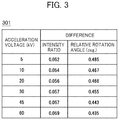
- FIG. 3 is a table showing the differences between the control amounts of image shift deflectors of the object lens center axis and those of the perpendicular incident axis;
- FIG. 4 is a table that is used for explaining incident angles obtained by the control by the image shift deflectors using several representative values
- FIG. 5 is a flowchart showing an adjustment sequence for setting the optical axis of a charged particle beam to the perpendicular incident axis using the representative values
- FIG. 6 is an overall block diagram of a scanning electron microscope according to a second embodiment
- FIG. 7A is a diagram explaining the object excitation dependency of a difference between intensity ratios
- FIG. 7B is a diagram explaining the object excitation dependency of the difference between relative rotation angles between deflection directions
- FIG. 8 is a flowchart showing an adjustment sequence for setting the optical axis of a charged particle beam to the perpendicular incident axis using a correction function
- FIG. 9 is a diagram showing an adjustment sequence for realizing a focus correction that cancels the shift of a visual field
- FIG. 10 is a diagram showing the configuration of the optical system of a scanning electron microscope.
- FIG. 11 is a diagram showing the configuration of an object lens.
- FIG. 1 is an overall block diagram of a scanning electron microscope according to a first embodiment.
- Primary electrons 102 emitted from an electron source 101 are converged by a condenser lens 114 , and after being deflected by an upper image shift deflector 103 , an upper deflector 104 , a lower image shift deflector 105 , and a lower deflector 106 , the primary electrons are condensed by an object lens 107 which is composed of an object lens coil 120 and an object lens magnetic path 121 , and irradiated to a specimen 108 .
- Secondary electrons 109 generated due to the irradiation of the primary electrons 102 to the specimen 108 are detected by a detector 110 .
- the specimen 108 is held on a specimen mounting table 111 , and the specimen mounting table 111 is configured to be movable in the horizontal and vertical directions with respect to the center axis of an electron optical system.
- the behaviors of the electron source 101 , the condenser lens 114 , the upper image shift deflector 103 , the upper deflector 104 , the lower image shift deflector 105 , the lower deflector 106 , the detector 110 , the object lens 107 , and the specimen mounting table 111 are controlled by a control unit 112 .
- a storage unit 113 stores parameters for controlling these components of the scanning electron microscope, and the control unit 112 reads out these parameters stored in the storage unit 113 , and performs control on these components.
- An observation region of the specimen 108 is two-dimensionally scanned with the primary electrons 102 to obtain an image. Such a two-dimensional scanning is performed by the upper deflector 104 and the lower deflector 106 .
- the shift of the visual field about ⁇ 10 ⁇ m is executed by the upper image shift deflector 103 and the lower image shift deflector 105 .
- the shift of the visual field can also be executed by the specimen mounting table 111 , because the behavior of the specimen mounting table 111 is a mechanical movement, it is difficult for the specimen mounting table 111 to move at high speed, and the accuracy of the shift of the visual field by the specimen mounting table 111 is low.
- the upper image shift deflector 103 and the lower image shift deflector 105 can provide the required shift amount more quickly and more accurately than the specimen mounting table 111 .
- FIG. 2A shows the trajectory 202 of primary electrons (hereinafter, referred to as the “object lens center axis”) subject to a normal image shift deflection.
- the primary electrons deflected by the upper image shift deflector 103 and the lower image shift deflector 105 pass through the object lens center 201 , and enter the visual field center 206 of the specimen 108 .
- the visual field center 206 is located at a position different from an intersection point of the central axis 205 of the electron optical system and the specimen 108 .
- the “object lens center” means the intersection point of the principal surface of the object lens 107 and the central axis 205 of the electron optical system.
- the incident angle of the primary electrons into the specimen 108 change in accordance with the deflection amount caused by the image shift deflectors. Therefore, in the observation, measurement, and the like of deep holes and deep grooves having high aspect ratios, the variation of this incident angle is not negligible.
- FIG. 2B is a diagram showing the trajectory 203 of primary electrons (hereinafter, referred to as the perpendicular incident axis) caused by perpendicular incident image shift deflection. Because the primary electrons enter the surface of the specimen 108 at right angle along the perpendicular incident axis 203 , this trajectory of the primary electrons is suitable for the observation, measurement, and the like of deep holes and deep grooves having high aspects. By making the perpendicular incident axis 203 pass through the outside of the object lens 201 , the perpendicular entry of the primary electrons into the surface of the specimen 108 is realized by the deflection operation of the upper image shift deflector 103 , the lower image shift deflector 105 , the object lens 107 .
- the object lens 107 is a magnetic field lens and exerts rotation movement on the primary electrons 102 , not only the deflection intensities but the deflection directions of the upper image shift deflector 103 and the lower image shift deflector 105 have to be changed so as to have appropriate values.
- the inventors of the present invention keenly examined a control method for realizing the perpendicular incident image shift deflection shown in FIG. 2B , and found out that, under the condition that a deceleration method is not applied to the specimen 108 , that is to say, for example, under the condition that a negative polarity retarding voltage is effectively not applied to the specimen 108 , the control amounts applied to the image shift deflectors in order for the optical axis of a charged particle beam to transfer from the object lens center axis 202 ( FIG. 2A ) to the perpendicular incident axis 203 ( FIG. 2B ) change little in accordance with the changes of the optical conditions typified by an acceleration voltage. This means that the perpendicular incident image shift deflection can be realized by a vastly-simplified control method.
- the object lens 107 functions as an electromagnetic field superimposing lens the electromagnetic field of which is composed of a magnetic field formed by the object lens coil 120 and the object lens magnetic path 121 and an electrostatic field formed by the retarding voltage. Therefore, if an acceleration voltage, which is one of main optical conditions, changes, the magnitude of the electrostatic field greatly changes, so that the position of the lens principal surface of the object lens 107 moves. Therefore, control performed by the image shift deflectors in this embodiment cannot be applied to an electron optical system to which the deceleration method is applied.
- FIG. 3 is Table 301 that shows differences between control amounts used for setting the optical axis of the charged particle beam to the object lens center axis 202 and control amounts used for setting the optical axis of the charged particle beam to the perpendicular incident axis 203 by respectively applying different acceleration voltages to the same visual field center 206 .
- the deflection amounts of primary electrons that enter the object lens 107 can be controlled with the use of an intensity ratio of the intensity of the upper image shift deflector 103 to the intensity of the lower image shift deflector 105 , and a relative rotation angle between the deflection directions of the upper image shift deflector 103 and the lower image shift deflector 105 .
- Table 301 shows the differences between the control amounts of image shift deflectors used for setting the optical axis of the charged particle beam to the object lens center axis 202 and those used for setting the optical axis of the charged particle beam to the perpendicular incident axis 203 as differences between two parameters.
- Two parameters are the intensity ratio of the intensity of the upper image shift deflector 103 to the intensity of the lower image shift deflector 105 , and the relative rotation angle between the deflection directions of the upper image shift deflector 103 and the lower image shift deflector 105 .
- FIG. 4 shows the calculated results of incident angles in the case of controlling the image shift deflectors using the representative values of the differences in Table 401 .
- FIG. 3 and FIG. 4 show the control amounts of the image shift deflectors under the same conditions.
- the column 402 shows the control amounts of the image shift deflectors for setting the optical axis of the charged particle beam to the object lens center axis 202
- the column 403 shows the representative values of differences ( FIG. 3 ) between the control amounts of the image shift deflectors for setting the optical axis of the charged particle beam to the object lens center axis 202
- the control amounts of the image shift deflectors for setting the optical axis of the charged particle beam to the perpendicular incident axis 203 shows the incident angles of primary electrons on the basis of the representative values of the differences (the column 403 ).
- simple average values are used as the representative values.
- incident angles obtained by control using the representative values of differences are equal to 0.01° or smaller. Even in the case of a high aspect-ratio shape having a high aspect ratio 50, the prospective angle of the shape is 0.57°, therefore incident angles obtained by control using the representative values are substantially small in comparison with the prospective angle of the high aspect-ratio shape that is a measurement target.
- differences between the control amounts of the image shift deflectors for setting the optical axis of the charged particle beam to the object lens center axis and the control amounts of the image shift deflectors for setting the optical axis of the charged particle beam to the perpendicular incident axis are calculated in advance under plural optical conditions, and the representative values of the differences are stored.
- the control amounts of the image shift deflectors for setting the optical axis of the charged particle beam to the object lens center axis is calculated, and the optical axis of the charged particle beam is set to the perpendicular incident axis by adding control based on the representative values of the differences to the above control amounts.
- control amounts for setting the optical axis of the charged particle beam to the object lens center axis 202 are given by Expression 1 using first control parameters (A, B, C, D).
- ISM1X and ISM1Y are LSB (least significant bit) values applied to the upper image shift deflector 103
- ISM2x and ISM2Y are LSB values applied to the lower image shift deflector 105 .
- Current amounts flowing through the respective image shift deflectors are controlled by these LSB values.
- the first control parameters in Expression 1 can be expressed by Expression 2 using an intensity ratio ⁇ 0 of the intensity of the upper image shift deflector 103 to the intensity of the lower image shift deflector 105 and a relative rotation angle ⁇ 0 between the deflection directions of the upper image shift deflector 103 and the lower image shift deflector 105 in the case of the optical axis of the charged particle beam being set to the object lens center axis 202 .
- the intensity ratio ⁇ 0 and the relative rotation angle ⁇ 0 between the deflection directions become values shown in the column 402 in FIG. 4 under a predefined optical condition.
- Control based on the differences (representative values) is performed for transferring the optical axis of the charged particle beam from the object lens center axis 202 to the perpendicular incident axis 203 .
- the control amounts of the image shift deflectors for setting the optical axis of the charged particle beam to the perpendicular incident axis 203 are given by Expression 3 using second control parameters (a, b, c, d).
- the second control parameters of Expression 3 are given by Expression 4 using the representative value ⁇ of differences between the intensity ratios of the intensities of the upper image shift deflector 103 to the intensities of the lower image shift deflector 105 in the case of the object lens center axis and those in the case of the perpendicular incident axis, and the representative value ⁇ of differences between the relative rotation angles between the deflection directions of the upper image shift deflector 103 and the deflection directions of the lower image shift deflector 105 in the case of the object lens center axis and those in the case of the perpendicular incident axis.
- the representative value ⁇ of the differences between the intensity ratios and the representative value ⁇ of the differences between the relative rotation angles between the deflection directions become values shown in the column 403 in FIG. 4 . Therefore, as the second parameters to be stored in the storage unit 113 of the scanning electron microscope, the representative value ⁇ of the differences between the intensity ratios of the intensities of the upper image shift deflector 103 to the intensities of the lower image shift deflector 105 and the representative value ⁇ of the differences between the relative rotation angles between the deflection directions of the upper image shift deflector 103 and the lower image shift deflector 105 can be stored, or the values of (a, b, c, d) can be stored instead.
- Expression 3 shows control that makes the optical axis of the charged particle beam set to the perpendicular incident angle by adjusting the LSB values (ISM2X and ISM2Y) of currents applied to the lower image shift deflector 105 on the basis of the LSB values (ISM1X and ISM1Y) of currents applied to the upper image shift deflector 103 .
- the first control parameters for setting the optical axis of the charged particle beam to the object lens center axis depends on the optical conditions of the electron optical system. However, because there are not many restrictions regarding the pattern of a specimen in the case of the object lens center axis, the object lens center axis 107 can be adjusted using a common axis adjustment technique such as a wobbling of the excitation intensity of an object lens 107 , for example. By fixing the second control parameters regardless of the optical conditions, it becomes possible to measure the specimen in a short time.
- This adjustment sequence is composed of a preliminary sequence and a principal sequence.
- the preliminary sequence is mainly executed before the shipment of the apparatus, or at the time of the installation of the apparatus, and the principal sequence is executed at the time when an operator uses the apparatus after the delivery of the apparatus.
- an intensity ratio of the intensity of the upper image shift deflector 103 to the intensity of the lower image shift deflector 105 and a relative rotation angle between the deflection directions of the upper image shift deflector 103 and the lower image shift deflector 105 in the case of setting the optical axis of the charged particle beam to the object lens center axis are obtained under plural optical conditions, for example, under plural acceleration voltages and modes.
- step S 503 an intensity ratio of the intensity of the upper image shift deflector 103 to the intensity of the lower image shift deflector 105 and a relative rotation angle between the deflection directions of the upper image shift deflector 103 and the lower image shift deflector 105 in the case of setting the optical axis of the charged particle beam to the perpendicular incident axis are obtained under the same optical conditions as at step S 502 .
- a difference between the intensity ratios of the intensities of the upper image shift deflector 103 to the intensities of the lower image shift deflector 105 and a difference between the relative rotation angles between the deflection directions of the upper image shift deflector 103 and the lower image shift deflector 105 obtained at step S 502 and those obtained at step S 503 are calculated for each optical condition.
- representative values are calculated from the difference values obtained at step S 504 .
- a calculation method of the representative values a method by which average values or median values are obtained can be used, or other statistical methods can be used. As shown in FIG.
- the incident angle of the perpendicular incident axis realized by the control of this embodiment has substantially small values, the differences among the values of the incident angle obtained by different calculation methods of the representative value are kept down at negligible levels.
- the representative values obtained at step S 505 are stored in the storage unit 113 as the second control parameters.
- step S 511 an operator sets optical conditions.
- step S 512 the intensity ratio of the intensity of the upper image shift deflector 103 to the intensity of the lower image shift deflector 105 and the relative rotation angle between the deflection directions of the upper image shift deflector 103 and the lower image shift deflector 105 at the object lens center axis, that is to say, the first parameters are readout from the storage unit 113 .
- step S 513 the first control parameters are updated by the axis adjustment of the object lens center axis.
- the first control parameters are updated using adjustment values obtained when the optical axis is adjusted so that the shift of an image does not occur when the focal length of the lens is periodically varied by a wobbler.
- the second parameters obtained in the preliminary sequence are read out from the storage unit 113 .
- the first control parameters are transformed by the second control parameters, and current amounts to be applied to the upper image shift deflector 103 and the lower image shift deflector 105 are calculated.
- control of the perpendicular incident axis can be realized through the above sequences.
- the optical conditions (steps S 502 and S 503 ) used for the adjustments in the preliminary sequence should include all optical conditions possessed by the apparatus, that is to say, all optical conditions that an operator can select in the principal sequence. For example, even if acceleration voltages that are not used for calculating the representative values in the preliminary sequence are used as acceleration voltages in the principal sequence, the perpendicular incident axis can be obtained.
- the optical conditions include not only acceleration voltages cited as examples, but also a mode (for example, a resolution priority mode, or a focal depth priority mode) can be selected as an optical condition.
- a mode for example, a resolution priority mode, or a focal depth priority mode
- switching between the modes such as the resolution priority mode and the focal depth priority mode is executed by changing the excitation amount of the condenser lens 114 so that the position of the object point (object surface) of primary electrons 102 is changed
- the optical axis of the charged particle beam can be set to the perpendicular incident axis by applying the representative value control of this embodiment regardless of what mode may be selected.
- a trajectory realized by the representative value control is not limited to the perpendicular incident axis, and it is also possible to form a trajectory having a desired incident angle using the representative value control.
- the control amounts for the upper image shift deflector 103 and the lower image shift deflector 105 are given by Expression 5.
- offset currents represented by a vector term (e, f) are added to the upper image shift deflector 103 and the lower image shift deflector 105 respectively.
- an offset vector term (e, f) obtained in advance by measurement it becomes possible to realize a trajectory having a desired incident angle. With this, even in the case where the side surface of a deep hole or a deep groove is slanting, measurement in an etching process, for example, can be flexibly performed.
- This embodiment can be applied to a system other than an electron optical system in which the position of the principal surface of an object lens is greatly changed, for example, an electron optical system to which a deceleration method is applied. Furthermore, this embodiment can be applied to a system to which a retarding method is applied if the retarding conditions are such weak retarding conditions as include a high-acceleration region with an acceleration voltage 5 kV or larger and a negative voltage about ⁇ 100 V applied to the specimen 108 . This is because, even if the retarding method is applied to the system, the shift of the principal surface associated with the changes of the retarding conditions is small.
- this embodiment includes three stages of deflectors, and control parameters used in this embodiment can be represented in various forms.
- FIG. 6 is an overall block diagram of a scanning electron microscope according to the second embodiment, and this overall block diagram has a configuration obtained by adding a correction function calculation unit 601 to the overall block diagram shown in FIG. 1 .
- FIG. 7A and FIG. 7B shows how the control amounts of the image shift deflectors needed for transfer from the object lens center axis to the perpendicular incident axis change in accordance with the excitation intensity of the object lens under predefined optical conditions.
- FIG. 7A shows a difference between an intensity ratio of the intensity of the upper image shift deflector 103 to the intensity of the lower image shift deflector 105 in the case of the object lens center axis and that in the case of the perpendicular incident axis
- FIG. 7A shows a difference between an intensity ratio of the intensity of the upper image shift deflector 103 to the intensity of the lower image shift deflector 105 in the case of the object lens center axis and that in the case of the perpendicular incident axis
- FIG. 7B shows a difference between a relative rotation angle between the deflection directions of the upper image shift deflector 103 and the lower image shift deflector 105 in the case of the object lens center axis and that in the case of the perpendicular incident axis.
- an intensity ratio of the intensity of the upper image shift deflector 103 to the intensity of the lower image shift deflector 105 and the relative rotation angle between the deflection directions of the upper image shift deflector 103 and the lower image shift deflector 105 can be corrected by using an appropriate function corresponding to an excitation intensity.
- such a change of the excitation intensity is generated when the focal position is changed in accordance with the height of a specimen to be observed or when the position of the object point of the primary electrons 102 is changed by controlling the excitation intensity of the condenser lens 114 .
- step S 805 in a preliminary sequence in FIG. 8 , the correction function is derived in the correction function calculation unit 601 using difference values obtained at step S 804 .
- the correction function is a function such as a polynominal expression or an exponential function, and the correction function is designated by an apparatus designer.
- Each coefficient of the correction function is derived using, for example, a least-squares method.
- step S 806 the derived correction function is stored in the storage unit 113 as second control parameters.
- step S 814 in a principal sequence, the values of the second control parameters are calculated using the excitation intensity of the object lens 107 and the correction function.
- correction function which is used for calculating the differences using the excitation intensity of the object lens 107 as a variable
- other parameters can be used as variables.
- the position of the object point of the primary electrons 102 can be set to a variable.
- the center position of the visual field is moved. This is because, in the case of the perpendicular incident axis 203 , primary electrons do not pass through the object lens center 201 of the object lens 107 . On the other hand, in the case of the object lens center axis 202 , primary electrons pass through the object lens center 201 of the object lens 107 , therefore the center position of the visual field is not moved even if the excitation intensity of the object lens 107 is changed.
- the shift amount of the visual field is the shift amount of the center of the visual field generated at the time when the optical axis of the charged particle beam is transferred from the object lens center axis to the perpendicular incident axis.
- This adjustment sequence is composed of a preliminary sequence and a principal sequence.
- the shift amounts of the visual field are measured by changing the excitation intensity of the object lens 107 in the case of the perpendicular incident axis under plural optical conditions, for example, under plural acceleration voltages.
- the shift amount of the visual field also depends on a deflection amount (a distance from the central axis 205 to the center position of the visual field) that is given by the deflectors to deflect primary electrons 102 .
- a correction coefficient for correcting the shift amount of the visual field corresponding to the deflection amount is derived at step S 904 .
- the relational expression obtained at step S 903 and the correction coefficient obtained at step S 904 are stored in the storage unit 113 .
- step S 911 an operator sets optical conditions. After the optical axis of the charged particle beam is set to the object lens center axis at step S 912 , a focus correction is executed at step S 913 .
- step S 914 excitation intensity after the focus correction is calculated.
- step S 915 the value of the excitation intensity calculated at step S 914 is substituted into the relational expression obtained in the preliminary sequence to calculate the value of the shift amount of the visual field.
- the shift amount of the visual field which is developed by transferring the optical axis of the charged particle beam from the object lens center axis to the perpendicular incident axis, is corrected so that the shift amount of the visual field is canceled.
- the shift amount of the visual field is corrected using the correction coefficient corresponding to the deflection amount.
- the optical axis of the charged particle beam is set to the perpendicular incident axis.
- the second control parameters are applied to the first control parameters that set the optical axis of the charged particle beam to the object lens center axis whose shift amount of the visual field is corrected.
- the present invention is not limited to these configurations.
- the image shift deflectors 103 and 105 used for the shift of the visual field, and the deflectors 104 and 106 used for photographing are installed between the electron source 101 and the object lens 107 in the configuration shown in FIG. 1 or FIG. 6
- the locations of the deflectors 104 and 106 are not limited to the locations shown in FIG. 1 or FIG. 6 . As shown in FIG.
- the upper deflector 104 and the lower deflector 106 are installed in such a way that both deflectors are sandwiched between the object lens 107 and the specimen 108 or the specimen mounting table 111 .
- the deflectors 104 and 106 which are used for photographing, are installed between the electron source 101 and the object lens 107 , there is an advantageous effect that the distance between the object lens 107 and the specimen 108 can be easily shortened.
- the deflectors 104 and 106 which are used for photographing, are installed between the object lens 107 and the specimen 108 , there is an advantageous effect that a wide visual field can be secured.
- the number of deflectors used for photographing should be two, and the number can be one or three or more.
- an object lens shown in FIG. 11 provides an image on a specimen 1106 with an electron beam using an electromagnetic lens, which includes an object lens magnetic path 1103 and an object lens coil 1102 , and an electrode 1101 .
- the openings of the magnetic paths of the electromagnetic lens look toward the optical axis of the electron beam, that is to say, the object lens is an out-lens type object lens, and not a semi-in-lens type object lens shown in FIG. 1 .
- the present invention can be applied to even such a type of object lens.
- the out-lens type object lens is characterized in that the shift of the principal surface of its own corresponding to the height of a specimen is practically negligible.
- This fact greatly contributes to the enhancement of the robustness of each of the first to third embodiments against the variation of the height of a specimen in the implementation of each of the first to third embodiments.
- two deflectors (the upper image shift deflector 1104 and the lower image shift deflector 1105 ) are located on the opposite side of the specimen 1106 with the openings of the magnetic paths of the object lens sandwiched between themselves and the specimen 1106 .
- the controls of the first to third embodiments to the two deflectors 1104 and 1105 , it becomes possible to generate deflection for setting the optical axis of the charged particle beam to the perpendicular incident axis.
Landscapes
- Chemical & Material Sciences (AREA)
- Analytical Chemistry (AREA)
- Electron Sources, Ion Sources (AREA)
- Length-Measuring Devices Using Wave Or Particle Radiation (AREA)
- Testing Or Measuring Of Semiconductors Or The Like (AREA)
Abstract
Description
a=(1+Δα)cos Δθ
b=−(1+Δα)sin Δθ
c=(1+Δα)sin Δθ
d=(1+Δα)cos Δθ
Claims (15)
Applications Claiming Priority (2)
| Application Number | Priority Date | Filing Date | Title |
|---|---|---|---|
| JP2017165432A JP6971090B2 (en) | 2017-08-30 | 2017-08-30 | Charged particle beam device |
| JP2017-165432 | 2017-08-30 |
Publications (2)
| Publication Number | Publication Date |
|---|---|
| US20190066969A1 US20190066969A1 (en) | 2019-02-28 |
| US10636618B2 true US10636618B2 (en) | 2020-04-28 |
Family
ID=65437638
Family Applications (1)
| Application Number | Title | Priority Date | Filing Date |
|---|---|---|---|
| US16/115,103 Active US10636618B2 (en) | 2017-08-30 | 2018-08-28 | Charged particle beam apparatus |
Country Status (3)
| Country | Link |
|---|---|
| US (1) | US10636618B2 (en) |
| JP (1) | JP6971090B2 (en) |
| KR (1) | KR102164232B1 (en) |
Families Citing this family (3)
| Publication number | Priority date | Publication date | Assignee | Title |
|---|---|---|---|---|
| JP7308581B2 (en) * | 2019-10-18 | 2023-07-14 | 株式会社日立ハイテクサイエンス | Charged particle beam device, composite charged particle beam device, and method of controlling charged particle beam device |
| JP2022021104A (en) * | 2020-07-21 | 2022-02-02 | 株式会社日立ハイテク | Charged particle beam device |
| WO2022130520A1 (en) * | 2020-12-16 | 2022-06-23 | 株式会社日立ハイテク | Pattern measurement device |
Citations (6)
| Publication number | Priority date | Publication date | Assignee | Title |
|---|---|---|---|---|
| JP2000156192A (en) | 1998-11-18 | 2000-06-06 | Jeol Ltd | Scanning electron microscope |
| JP2007187538A (en) | 2006-01-13 | 2007-07-26 | Hitachi High-Technologies Corp | Charged particle beam apparatus and image acquisition method using the same |
| US20100282596A1 (en) | 2007-12-26 | 2010-11-11 | Nawotec Gmbh | Methods and systems for removing a material from a sample |
| US20120286160A1 (en) | 2011-05-09 | 2012-11-15 | Hitachi High-Technologies Corporation | Charged particle instrument |
| JP2014053074A (en) | 2012-09-05 | 2014-03-20 | Hitachi High-Technologies Corp | Charged particle beam device |
| US20160217967A1 (en) * | 2015-01-26 | 2016-07-28 | Hitachi High-Technologies Corporation | Charged Particle Beam Device |
-
2017
- 2017-08-30 JP JP2017165432A patent/JP6971090B2/en active Active
-
2018
- 2018-08-03 KR KR1020180090644A patent/KR102164232B1/en active Active
- 2018-08-28 US US16/115,103 patent/US10636618B2/en active Active
Patent Citations (9)
| Publication number | Priority date | Publication date | Assignee | Title |
|---|---|---|---|---|
| JP2000156192A (en) | 1998-11-18 | 2000-06-06 | Jeol Ltd | Scanning electron microscope |
| JP2007187538A (en) | 2006-01-13 | 2007-07-26 | Hitachi High-Technologies Corp | Charged particle beam apparatus and image acquisition method using the same |
| US20110133080A1 (en) | 2006-01-13 | 2011-06-09 | Chie Shishido | Charged particel beam apparatus and methods for capturing images using the same |
| US20100282596A1 (en) | 2007-12-26 | 2010-11-11 | Nawotec Gmbh | Methods and systems for removing a material from a sample |
| JP2011508943A (en) | 2007-12-26 | 2011-03-17 | ナヴォテック ゲーエムベーハー | Apparatus and method for analyzing and / or processing samples |
| US20120286160A1 (en) | 2011-05-09 | 2012-11-15 | Hitachi High-Technologies Corporation | Charged particle instrument |
| JP2012234754A (en) | 2011-05-09 | 2012-11-29 | Hitachi High-Technologies Corp | Charged particle beam device |
| JP2014053074A (en) | 2012-09-05 | 2014-03-20 | Hitachi High-Technologies Corp | Charged particle beam device |
| US20160217967A1 (en) * | 2015-01-26 | 2016-07-28 | Hitachi High-Technologies Corporation | Charged Particle Beam Device |
Non-Patent Citations (2)
| Title |
|---|
| Office Action dated Aug. 19, 2019 in counterpart Korean Application 10-2018-0090644. |
| Office Action dated Feb. 14, 2020 in counterpart Korean Application 10-2018-0090644. |
Also Published As
| Publication number | Publication date |
|---|---|
| JP2019046567A (en) | 2019-03-22 |
| JP6971090B2 (en) | 2021-11-24 |
| KR102164232B1 (en) | 2020-10-12 |
| KR20190024685A (en) | 2019-03-08 |
| US20190066969A1 (en) | 2019-02-28 |
Similar Documents
| Publication | Publication Date | Title |
|---|---|---|
| USRE49784E1 (en) | Apparatus of plural charged-particle beams | |
| KR102566320B1 (en) | Charged Particle Beam Device, Field Curvature Corrector, and Methods of Operating a Charged Particle Beam Device | |
| JP5498955B2 (en) | Apparatus and method for analyzing and / or processing samples | |
| JP2023527047A (en) | High throughput multi-beam charged particle inspection system with dynamic control | |
| KR101477558B1 (en) | Charged particle beam writing method and charged particle beam writing apparatus | |
| TW201637062A (en) | Charged particle beam system and method | |
| KR102778909B1 (en) | Multi-charged particle beam control method, multi-charged particle beam irradiation method and multi-charged particle beam irradiation device | |
| US20110310373A1 (en) | Lithography apparatus and device manufacturing method | |
| US10636618B2 (en) | Charged particle beam apparatus | |
| KR20180111579A (en) | Electron-beam irradiation apparatus and dynamic focus adjusting method of electron-beam | |
| JP4679978B2 (en) | Charged particle beam application equipment | |
| JP2004342341A (en) | Mirror electron microscope and pattern defect inspection apparatus using the same | |
| US20150325404A1 (en) | Lithography apparatus and method, and method of manufacturing an article | |
| US20150364291A1 (en) | Lithography apparatus, and method of manufacturing article | |
| EP2388801B1 (en) | Multi-column electron beam lithography system and electron beam orbit adjusting method thereof | |
| US8927949B2 (en) | Measuring apparatus, drawing apparatus, and article manufacturing method | |
| KR20140130029A (en) | Drawing apparatus, and method of manufacturing article | |
| KR101790829B1 (en) | Drawing apparatus, and method of manufacturing article | |
| JP2015035563A (en) | Drawing data generation method, processing device, program, drawing device, and article manufacturing method | |
| US20150044614A1 (en) | Drawing apparatus, and method of manufacturing article | |
| KR102811445B1 (en) | Method for adjusting optical system of multi-charged particle beam device and computer readable recording medium | |
| US20080135786A1 (en) | Adjustable aperture element for particle beam device, method of operating and manufacturing thereof | |
| JP6901374B2 (en) | Charged particle beam drawing device | |
| US10483082B2 (en) | Evaluation method, correction method, recording medium and electron beam lithography system | |
| JP2016115811A (en) | Drawing apparatus, and manufacturing method for article |
Legal Events
| Date | Code | Title | Description |
|---|---|---|---|
| FEPP | Fee payment procedure |
Free format text: ENTITY STATUS SET TO UNDISCOUNTED (ORIGINAL EVENT CODE: BIG.); ENTITY STATUS OF PATENT OWNER: LARGE ENTITY |
|
| AS | Assignment |
Owner name: HITACHI HIGH-TECHNOLOGIES CORPORATION, JAPAN Free format text: ASSIGNMENT OF ASSIGNORS INTEREST;ASSIGNORS:BIZEN, KAORI;SOHDA, YASUNARI;SAKAKIBARA, MAKOTO;AND OTHERS;SIGNING DATES FROM 20180820 TO 20180822;REEL/FRAME:047055/0789 |
|
| STPP | Information on status: patent application and granting procedure in general |
Free format text: DOCKETED NEW CASE - READY FOR EXAMINATION |
|
| STPP | Information on status: patent application and granting procedure in general |
Free format text: NON FINAL ACTION MAILED |
|
| STPP | Information on status: patent application and granting procedure in general |
Free format text: RESPONSE TO NON-FINAL OFFICE ACTION ENTERED AND FORWARDED TO EXAMINER |
|
| STPP | Information on status: patent application and granting procedure in general |
Free format text: NOTICE OF ALLOWANCE MAILED -- APPLICATION RECEIVED IN OFFICE OF PUBLICATIONS |
|
| AS | Assignment |
Owner name: HITACHI HIGH-TECH CORPORATION, JAPAN Free format text: CHANGE OF NAME;ASSIGNOR:HITACHI HIGH-TECHNOLOGIES CORPORATION;REEL/FRAME:052225/0894 Effective date: 20200214 |
|
| STCF | Information on status: patent grant |
Free format text: PATENTED CASE |
|
| MAFP | Maintenance fee payment |
Free format text: PAYMENT OF MAINTENANCE FEE, 4TH YEAR, LARGE ENTITY (ORIGINAL EVENT CODE: M1551); ENTITY STATUS OF PATENT OWNER: LARGE ENTITY Year of fee payment: 4 |