US10629547B1 - Redistribution-layer fanout package stiffener - Google Patents
Redistribution-layer fanout package stiffener Download PDFInfo
- Publication number
- US10629547B1 US10629547B1 US16/174,871 US201816174871A US10629547B1 US 10629547 B1 US10629547 B1 US 10629547B1 US 201816174871 A US201816174871 A US 201816174871A US 10629547 B1 US10629547 B1 US 10629547B1
- Authority
- US
- United States
- Prior art keywords
- packaging substrate
- substrate
- stiffener structure
- semiconductor device
- path
- Prior art date
- Legal status (The legal status is an assumption and is not a legal conclusion. Google has not performed a legal analysis and makes no representation as to the accuracy of the status listed.)
- Active
Links
Images


Classifications
-
- H—ELECTRICITY
- H10—SEMICONDUCTOR DEVICES; ELECTRIC SOLID-STATE DEVICES NOT OTHERWISE PROVIDED FOR
- H10W—GENERIC PACKAGES, INTERCONNECTIONS, CONNECTORS OR OTHER CONSTRUCTIONAL DETAILS OF DEVICES COVERED BY CLASS H10
- H10W70/00—Package substrates; Interposers; Redistribution layers [RDL]
- H10W70/60—Insulating or insulated package substrates; Interposers; Redistribution layers
- H10W70/611—Insulating or insulated package substrates; Interposers; Redistribution layers for connecting multiple chips together
-
- H—ELECTRICITY
- H10—SEMICONDUCTOR DEVICES; ELECTRIC SOLID-STATE DEVICES NOT OTHERWISE PROVIDED FOR
- H10W—GENERIC PACKAGES, INTERCONNECTIONS, CONNECTORS OR OTHER CONSTRUCTIONAL DETAILS OF DEVICES COVERED BY CLASS H10
- H10W90/00—Package configurations
- H10W90/701—Package configurations characterised by the relative positions of pads or connectors relative to package parts
-
- H01L23/562—
-
- H01L23/49827—
-
- H01L23/49866—
-
- H01L25/50—
-
- H—ELECTRICITY
- H10—SEMICONDUCTOR DEVICES; ELECTRIC SOLID-STATE DEVICES NOT OTHERWISE PROVIDED FOR
- H10W—GENERIC PACKAGES, INTERCONNECTIONS, CONNECTORS OR OTHER CONSTRUCTIONAL DETAILS OF DEVICES COVERED BY CLASS H10
- H10W42/00—Arrangements for protection of devices
- H10W42/121—Arrangements for protection of devices protecting against mechanical damage
-
- H—ELECTRICITY
- H10—SEMICONDUCTOR DEVICES; ELECTRIC SOLID-STATE DEVICES NOT OTHERWISE PROVIDED FOR
- H10W—GENERIC PACKAGES, INTERCONNECTIONS, CONNECTORS OR OTHER CONSTRUCTIONAL DETAILS OF DEVICES COVERED BY CLASS H10
- H10W70/00—Package substrates; Interposers; Redistribution layers [RDL]
- H10W70/60—Insulating or insulated package substrates; Interposers; Redistribution layers
- H10W70/62—Insulating or insulated package substrates; Interposers; Redistribution layers characterised by their interconnections
- H10W70/63—Vias, e.g. via plugs
- H10W70/635—Through-vias
-
- H—ELECTRICITY
- H10—SEMICONDUCTOR DEVICES; ELECTRIC SOLID-STATE DEVICES NOT OTHERWISE PROVIDED FOR
- H10W—GENERIC PACKAGES, INTERCONNECTIONS, CONNECTORS OR OTHER CONSTRUCTIONAL DETAILS OF DEVICES COVERED BY CLASS H10
- H10W70/00—Package substrates; Interposers; Redistribution layers [RDL]
- H10W70/60—Insulating or insulated package substrates; Interposers; Redistribution layers
- H10W70/62—Insulating or insulated package substrates; Interposers; Redistribution layers characterised by their interconnections
- H10W70/65—Shapes or dispositions of interconnections
-
- H—ELECTRICITY
- H10—SEMICONDUCTOR DEVICES; ELECTRIC SOLID-STATE DEVICES NOT OTHERWISE PROVIDED FOR
- H10W—GENERIC PACKAGES, INTERCONNECTIONS, CONNECTORS OR OTHER CONSTRUCTIONAL DETAILS OF DEVICES COVERED BY CLASS H10
- H10W70/00—Package substrates; Interposers; Redistribution layers [RDL]
- H10W70/60—Insulating or insulated package substrates; Interposers; Redistribution layers
- H10W70/62—Insulating or insulated package substrates; Interposers; Redistribution layers characterised by their interconnections
- H10W70/66—Conductive materials thereof
-
- H—ELECTRICITY
- H10—SEMICONDUCTOR DEVICES; ELECTRIC SOLID-STATE DEVICES NOT OTHERWISE PROVIDED FOR
- H10W—GENERIC PACKAGES, INTERCONNECTIONS, CONNECTORS OR OTHER CONSTRUCTIONAL DETAILS OF DEVICES COVERED BY CLASS H10
- H10W90/00—Package configurations
-
- H—ELECTRICITY
- H10—SEMICONDUCTOR DEVICES; ELECTRIC SOLID-STATE DEVICES NOT OTHERWISE PROVIDED FOR
- H10W—GENERIC PACKAGES, INTERCONNECTIONS, CONNECTORS OR OTHER CONSTRUCTIONAL DETAILS OF DEVICES COVERED BY CLASS H10
- H10W76/00—Containers; Fillings or auxiliary members therefor; Seals
- H10W76/40—Fillings or auxiliary members in containers, e.g. centering rings
-
- H—ELECTRICITY
- H10—SEMICONDUCTOR DEVICES; ELECTRIC SOLID-STATE DEVICES NOT OTHERWISE PROVIDED FOR
- H10W—GENERIC PACKAGES, INTERCONNECTIONS, CONNECTORS OR OTHER CONSTRUCTIONAL DETAILS OF DEVICES COVERED BY CLASS H10
- H10W90/00—Package configurations
- H10W90/701—Package configurations characterised by the relative positions of pads or connectors relative to package parts
- H10W90/721—Package configurations characterised by the relative positions of pads or connectors relative to package parts of bump connectors
- H10W90/724—Package configurations characterised by the relative positions of pads or connectors relative to package parts of bump connectors between a chip and a stacked insulating package substrate, interposer or RDL
Definitions
- This disclosure related generally to redistribution layer fanout packaging, and in particular to stiffeners uses to reinforce redistribution layer fanout packaging.
- Packaging semiconductor devices together presents many benefits for streamlining the manufacture of computer processors, memories, and products.
- individual semiconductor devices are formed and then coupled with other semiconductor devices to form a system.
- a packaging substrate may be used to couple the devices to each other.
- a packaging substrate may include a fanout layer that expands connection sizes from the semiconductor devices to enable connection to larger computing systems.
- metal layers route connections from devices on a first side of the redistribution layer to connections on a second side of the redistribution layer.
- packaged devices may be subject to forces or pressures as they are assembled into computing devices. In some cases, weak portions of the packages may be vulnerable to breaks during subsequent assembly procedures.
- Each of the devices attached to the redistribution layer may add structural integrity to the overall package. However, a typical redistribution layer may have still have vulnerabilities between the attached devices. These vulnerabilities may reduce the production rate of functional packaged devices. Other disadvantages may exist.
- FIG. 1 depicts a top view of an embodiment of a semiconductor package assembly.
- FIG. 2 depicts a side view of an embodiment of a semiconductor package assembly.
- FIG. 3 depicts a top view of an embodiment of a semiconductor package assembly.
- FIG. 4 depicts a top view of an embodiment of a semiconductor package assembly.
- FIG. 5 depicts a cross-section view of an embodiment of a semiconductor package assembly.
- FIG. 6 is a flow chart depicting an embodiment of a method for forming an embodiment of a semiconductor package assembly.
- semiconductor device assembly can refer to an assembly of one or more semiconductor devices, semiconductor device packages, and/or substrates, which may include interposers, supports, and/or other suitable substrates.
- the semiconductor device assembly may be manufactured as, but not limited to, discrete package form, strip or matrix form, and/or wafer panel form.
- semiconductor device generally refers to a solid-state device that includes semiconductor material.
- a semiconductor device can include, for example, a semiconductor substrate, wafer, panel, or a single die from a wafer or substrate.
- a semiconductor device may further include one or more device layers deposited on a substrate.
- a semiconductor device may refer herein to a semiconductor die, but semiconductor devices are not limited to semiconductor dies.
- semiconductor device package can refer to an arrangement with one or more semiconductor devices incorporated into a common package.
- a semiconductor package can include a housing or casing that partially or completely encapsulates at least one semiconductor device.
- a semiconductor package can also include a substrate that carries one or more semiconductor devices. The substrate may be attached to or otherwise incorporate within the housing or casing.
- the terms “vertical,” “lateral,” “upper,” and “lower” can refer to relative directions or positions of features in the semiconductor devices and/or semiconductor device assemblies shown in the Figures. For example, “upper” or “uppermost” can refer to a feature positioned closer to the top of a page than another feature. These terms, however, should be construed broadly to include semiconductor devices and/or semiconductor device assemblies having other orientations, such as inverted or inclined orientations where top/bottom, over/under, above/below, up/down, and left/right can be interchanged depending on the orientation.
- an apparatus in one embodiment, includes a packaging substrate.
- the apparatus further includes multiple semiconductor devices attached to the packaging substrate.
- the multiple semiconductor devices define a path along the packaging substrate between a pair of the multiple semiconductor devices.
- the apparatus further includes a stiffener structure coupled to the packaging substrate and positioned with a longitudinal axis of the stiffener structure being perpendicular to the path.
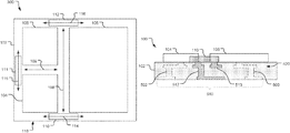
- the assembly 100 may include a substrate 102 .
- the substrate 102 may be a semiconductor device packaging substrate and, in particular, may include a redistribution layer.
- the redistribution layer may include copper leads forming a fanout structure.
- the assembly 100 may include a first semiconductor device 104 and a second semiconductor device 105 .
- the semiconductor devices 104 , 105 may correspond to any devices that may be packaged together, including processors, memory arrays, and/or other types of integrated circuit device components.
- the first semiconductor device 104 and the second semiconductor device 105 may define a path 108 along the substrate 102 between the semiconductor devices 104 , 105 .
- the path 108 may correspond to an area between the semiconductor devices 104 , 105 that is not covered by the semiconductor devices 104 , 105 .
- the attachment of the semiconductor devices 104 , 105 may provide some additional structural rigidity to the substrate 102 at the portions that are covered by the semiconductor devices 104 , 105 .
- the area around the path 108 that is not covered by the semiconductor devices may not have the benefit of being strengthened by the attached semiconductor devices.
- a stiffener structure 110 may be coupled to the substrate 102 .
- the stiffener structure 110 may have a longitudinal axis 114 that is perpendicular to the path 108 .
- the stiffener structure 110 may include copper, aluminum, silver, another type of conductive material, or a combination thereof.
- the material of the stiffener structure 110 may be selected to match a coefficient of thermal expansion of the substrate 102 and or one or more layers positioned within the substrate 102 .
- the stiffener structure 110 may include copper for coefficient of thermal expansion matching purposes.
- the coefficient of thermal expansion of the stiffener structure 110 may be substantially equal to the coefficient of thermal expansion of the substrate 102 .
- the stiffener structure 110 may be positioned proximate to an edge 118 of the substrate 102 .
- proximate means that the stiffener structure 110 is as close, or closer to the edge 118 of the substrate 102 than other structures (e.g., the semiconductor devices 104 , 105 ) attached to a surface of the substrate 102 .
- a benefit of the assembly 100 is that by including the stiffener structure 110 , the assembly as a whole may be strengthened, particularly along the path 108 . By strengthening between the semiconductor devices 104 , 105 , fewer breaks, cracks, and/or other failures may occur within the substrate 102 . As such, an output of mass produced semiconductor package assemblies may be increased. Other advantages may exist.
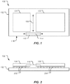
- a semiconductor package assembly 100 may include a substrate 102 with a first semiconductor device 104 , and a second semiconductor device 105 coupled thereto.
- the first semiconductor device 104 may be coupled to the substrate 102 via a first ball-grid-array structure 202 .
- the second semiconductor device 105 may be coupled to the substrate 102 via a second ball-grid-array structure 204 .
- a ball-grid-array is depicted in FIG. 2 , other connection mechanisms may be used.
- the first semiconductor device 104 may inherently add some structural rigidity to the substrate 102 directly under the first semiconductor device 104 .
- the second semiconductor device 105 may inherently add some structural rigidity to the substrate 102 directly under the second semiconductor device 105 .
- a stiffener structure 110 may also be coupled to the substrate 102 in order to provide additional rigidity between the semiconductor devices 104 , 105 .
- a length, width, and height of the stiffener structure 110 may be selected to provide a desired balance between rigidity, spacing, and cost effectiveness.
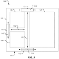
- the semiconductor package assembly 300 may include a substrate 102 , a first semiconductor device 104 and a second semiconductor device 105 .
- the semiconductor package assembly 300 may further include a third semiconductor device 106 .
- a pair of the semiconductor devices 104 - 106 may define a first path 108 defined between the pair of semiconductor devices (e.g., either the first and second semiconductor devices 104 , 105 or the second and third semiconductor devices 105 , 106 ).
- Another pair of the semiconductor devices 104 - 106 may define a second path 109 between the pair.
- the assembly 300 may include multiple stiffener structures 110 - 112 .
- a first stiffener structure 110 may be positioned proximate to an edge 118 of the substrate 102 , having a longitudinal axis 114 perpendicular to the path 108 .
- a second stiffener structure 111 may be positioned having a longitudinal axis 115 perpendicular to the path 109 .
- a third stiffener structure 112 may be positioned having a longitudinal axis 116 perpendicular to the path 108 .
- Other configurations are possible.
- a benefit of the assembly 300 is that multiple portions of the substrate 102 may be strengthened by the multiple stiffener structures 110 - 112 . Other benefits may exist.
- the assembly 400 may include a substrate 102 with a first semiconductor device 104 , a second semiconductor device 105 , and a third semiconductor device 106 .
- the assembly 400 may include a single stiffener structure that is a frame 410 attached along a border of the substrate 102 .
- a portion of the frame 410 may have a longitudinal axis 414 that runs perpendicular to a path 108 between the first semiconductor device 104 and the second semiconductor device 105 .
- Another portion of the frame 410 may have a longitudinal axis 415 that runs perpendicular to a path 109 between the first semiconductor device 104 and the third semiconductor device 106 .
- Yet another portion of the frame 410 may have a longitudinal axis 416 that runs perpendicular to the path 108 between the second semiconductor device 105 and the third semiconductor device 106 .
- the frame 410 may enable the assembly 400 to be manufactured without determining specific points that are to be strengthened. Rather, the entire border of the substrate 102 may be strengthened and made more rigid. Other advantages may exist.
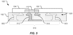
- FIG. 5 a cross-section view of a semiconductor package assembly 100 is depicted.
- FIG. 5 depicts additional details that may corresponding to the substrate 102 .
- the substrate 102 may include a first electrode 502 coupled to the first semiconductor device 104 .
- the substrate 102 may further include a second electrode 503 coupled to the second semiconductor device 105 .
- the substrate 102 may include many additional electrodes, which have not been shown, creating electrical pathways through the substrate 102 for connecting the package assembly 100 to another device (e.g., a printed circuit board or another type of system board), and for connecting the semiconductor devices 104 , 105 to each other.
- the substrate 102 may be a redistribution layer substrate and the electrodes 502 , 503 may correspond to a fanout structure 510 positioned in the substrate 102 .
- the substrate 102 may include a molding compound 520 within which the electrodes 502 , 503 are formed.
- the electrodes 502 , 503 may form part of a copper fanout structure 510 .
- FIG. 5 has been greatly simplified for ease of description. It should also be understood that one or more connection mechanisms (not shown) may be used to couple the semiconductor devices 104 , 105 to their respective electrodes 502 , 503 .
- the stiffener structure 110 may be coupled to a first additional electrode 512 and a second additional electrode 513 . In this configuration, the stiffener structure 110 may function as a jumper between electrodes in addition to providing structural rigidity to the substrate 102 .
- a material of the stiffener structure 110 may be selected to match a coefficient of thermal expansion of the fanout structure 510 including the electrodes 502 , 503 and including the additional electrodes 512 , 513 .
- the fanout structure 510 is a copper fanout structure and the stiffener structure 110 includes copper. Other materials are possible.
- the stiffener structure 110 may be further anchored to the substrate 102 , adding rigidity to the overall structure. Further, the stiffener structure 110 may be used to conduct electrical signals, thereby adding functionality and potentially making the assembly 100 more efficient. Other advantages may exist.
- the method 600 may include attaching a first semiconductor device to a packaging substrate, at 602 .
- the first semiconductor device 104 may be attached to the substrate 102 .
- the method 600 may further include attaching a second semiconductor device to the packaging substrate, the first semiconductor device and the second semiconductor device defining a path therebetween along the packaging substrate, at 604 .
- the second semiconductor device 105 may be attached to the substrate 102 defining the path 108 therebetween along the substrate 102 .
- the method 600 may also include selecting a material of a stiffener structure to match a coefficient of thermal expansion of the packaging substrate, at 606 .
- a material of the stiffener structure 110 may be selected to match a coefficient of thermal expansion of the substrate 102 (which may be based on a fanout structure 510 embedded within the substrate 102 ).
- the method 600 may include attaching the stiffener structure to the packaging substrate with a longitudinal axis of the stiffener structure being perpendicular to the path, at 608 .
- the stiffener structure 110 may be attached to the substrate 102 with the longitudinal axis 114 of the stiffener structure 110 perpendicular to the path 108 .
- a benefit of the method 600 is that a packaging assembly may be constructed with more rigidity between semiconductor devices attached to a packaging substrate than typical packaging assemblies that do not include the stiffener structure 110 . Other advantages may exist.
Landscapes
- Cooling Or The Like Of Semiconductors Or Solid State Devices (AREA)
- Engineering & Computer Science (AREA)
- Manufacturing & Machinery (AREA)
Abstract
Description
Claims (16)
Priority Applications (2)
| Application Number | Priority Date | Filing Date | Title |
|---|---|---|---|
| US16/174,871 US10629547B1 (en) | 2018-10-30 | 2018-10-30 | Redistribution-layer fanout package stiffener |
| CN201911037939.4A CN111128947A (en) | 2018-10-30 | 2019-10-29 | Heavy cloth layer fan-out type encapsulation reinforcement |
Applications Claiming Priority (1)
| Application Number | Priority Date | Filing Date | Title |
|---|---|---|---|
| US16/174,871 US10629547B1 (en) | 2018-10-30 | 2018-10-30 | Redistribution-layer fanout package stiffener |
Publications (2)
| Publication Number | Publication Date |
|---|---|
| US10629547B1 true US10629547B1 (en) | 2020-04-21 |
| US20200135658A1 US20200135658A1 (en) | 2020-04-30 |
Family
ID=70285120
Family Applications (1)
| Application Number | Title | Priority Date | Filing Date |
|---|---|---|---|
| US16/174,871 Active US10629547B1 (en) | 2018-10-30 | 2018-10-30 | Redistribution-layer fanout package stiffener |
Country Status (2)
| Country | Link |
|---|---|
| US (1) | US10629547B1 (en) |
| CN (1) | CN111128947A (en) |
Citations (2)
| Publication number | Priority date | Publication date | Assignee | Title |
|---|---|---|---|---|
| US20180261528A1 (en) * | 2017-03-08 | 2018-09-13 | Mediatek Inc. | Semiconductor package with improved heat dissipation |
| US20190206807A1 (en) * | 2017-12-28 | 2019-07-04 | Samsung Electronics Co., Ltd. | Semiconductor package |
Family Cites Families (2)
| Publication number | Priority date | Publication date | Assignee | Title |
|---|---|---|---|---|
| US9312193B2 (en) * | 2012-11-09 | 2016-04-12 | Taiwan Semiconductor Manufacturing Company, Ltd. | Stress relief structures in package assemblies |
| US20180151461A1 (en) * | 2016-11-29 | 2018-05-31 | Globalfoundries Inc. | Stiffener for fan-out wafer level packaging and method of manufacturing |
-
2018
- 2018-10-30 US US16/174,871 patent/US10629547B1/en active Active
-
2019
- 2019-10-29 CN CN201911037939.4A patent/CN111128947A/en not_active Withdrawn
Patent Citations (2)
| Publication number | Priority date | Publication date | Assignee | Title |
|---|---|---|---|---|
| US20180261528A1 (en) * | 2017-03-08 | 2018-09-13 | Mediatek Inc. | Semiconductor package with improved heat dissipation |
| US20190206807A1 (en) * | 2017-12-28 | 2019-07-04 | Samsung Electronics Co., Ltd. | Semiconductor package |
Also Published As
| Publication number | Publication date |
|---|---|
| CN111128947A (en) | 2020-05-08 |
| US20200135658A1 (en) | 2020-04-30 |
Similar Documents
| Publication | Publication Date | Title |
|---|---|---|
| US8623706B2 (en) | Microelectronic package with terminals on dielectric mass | |
| US7109572B2 (en) | Quad flat no lead (QFN) grid array package | |
| US7612436B1 (en) | Packaged microelectronic devices with a lead frame | |
| US20070164457A1 (en) | Semiconductor package, substrate with conductive post, stacked type semiconductor device, manufacturing method of semiconductor package and manufacturing method of stacked type semiconductor device | |
| US20040005733A1 (en) | Method of manufacturing semiconductor device | |
| US20090045508A1 (en) | Oblong peripheral solder ball pads on a printed circuit board for mounting a ball grid array package | |
| US20110272825A1 (en) | Stacked die assembly having reduced stress electrical interconnects | |
| JPH07288309A (en) | Semiconductor device, manufacturing method thereof, and semiconductor module | |
| US7950144B2 (en) | Method for controlling warpage in redistributed chip packaging panels | |
| US8816480B2 (en) | Electronic device packages and methods of manufacturing the same | |
| US7095096B1 (en) | Microarray lead frame | |
| KR100711675B1 (en) | Semiconductor device and manufacturing method thereof | |
| US20070029668A1 (en) | Package module having a stacking platform | |
| US9760132B2 (en) | Stiffening electronic packages by disposing a stiffener ring between substrate center area and conductive pad | |
| US10629547B1 (en) | Redistribution-layer fanout package stiffener | |
| US8648453B2 (en) | Semiconductor device and method for manufacturing the same | |
| EP0930646A2 (en) | Lead-on-chip type semicoductor device having thin plate and method for manufacturing the same | |
| US11581231B2 (en) | Stress tuned stiffeners for micro electronics package warpage control | |
| US9123712B1 (en) | Leadframe system with warp control mechanism and method of manufacture thereof | |
| US20040075176A1 (en) | Packaged semiconductor device | |
| US8912046B2 (en) | Integrated circuit packaging system with lead frame and method of manufacture thereof | |
| US20120133036A1 (en) | Integrated circuit packaging system with connection supports and method of manufacture thereof | |
| US20250118611A1 (en) | Electronic package assembly and a method for forming the same | |
| US12368113B2 (en) | Methods and apparatus for using spacer-on-spacer design for solder joint reliability improvement in semiconductor devices | |
| US10985129B2 (en) | Mitigating cracking within integrated circuit (IC) device carrier |
Legal Events
| Date | Code | Title | Description |
|---|---|---|---|
| AS | Assignment |
Owner name: MICRON TECHNOLOGY, INC., IDAHO Free format text: ASSIGNMENT OF ASSIGNORS INTEREST;ASSIGNOR:LIN, JING CHENG;REEL/FRAME:047356/0692 Effective date: 20181030 |
|
| FEPP | Fee payment procedure |
Free format text: ENTITY STATUS SET TO UNDISCOUNTED (ORIGINAL EVENT CODE: BIG.); ENTITY STATUS OF PATENT OWNER: LARGE ENTITY |
|
| AS | Assignment |
Owner name: JPMORGAN CHASE BANK, N.A., AS COLLATERAL AGENT, ILLINOIS Free format text: SUPPLEMENT NO. 3 TO PATENT SECURITY AGREEMENT;ASSIGNOR:MICRON TECHNOLOGY, INC.;REEL/FRAME:048951/0902 Effective date: 20190416 Owner name: MORGAN STANLEY SENIOR FUNDING, INC., AS COLLATERAL AGENT, MARYLAND Free format text: SUPPLEMENT NO. 12 TO PATENT SECURITY AGREEMENT;ASSIGNOR:MICRON TECHNOLOGY, INC.;REEL/FRAME:048948/0677 Effective date: 20190416 |
|
| AS | Assignment |
Owner name: MICRON TECHNOLOGY, INC., IDAHO Free format text: RELEASE BY SECURED PARTY;ASSIGNOR:MORGAN STANLEY SENIOR FUNDING, INC., AS COLLATERAL AGENT;REEL/FRAME:050724/0392 Effective date: 20190731 |
|
| AS | Assignment |
Owner name: MICRON TECHNOLOGY, INC., IDAHO Free format text: RELEASE BY SECURED PARTY;ASSIGNOR:JPMORGAN CHASE BANK, N.A., AS COLLATERAL AGENT;REEL/FRAME:051041/0317 Effective date: 20190731 |
|
| STCF | Information on status: patent grant |
Free format text: PATENTED CASE |
|
| MAFP | Maintenance fee payment |
Free format text: PAYMENT OF MAINTENANCE FEE, 4TH YEAR, LARGE ENTITY (ORIGINAL EVENT CODE: M1551); ENTITY STATUS OF PATENT OWNER: LARGE ENTITY Year of fee payment: 4 |