US10621943B2 - Display device driver having pixel drive voltage delay selection - Google Patents
Display device driver having pixel drive voltage delay selection Download PDFInfo
- Publication number
- US10621943B2 US10621943B2 US15/205,089 US201615205089A US10621943B2 US 10621943 B2 US10621943 B2 US 10621943B2 US 201615205089 A US201615205089 A US 201615205089A US 10621943 B2 US10621943 B2 US 10621943B2
- Authority
- US
- United States
- Prior art keywords
- pixel drive
- pixel
- delay
- drive voltage
- signal
- Prior art date
- Legal status (The legal status is an assumption and is not a legal conclusion. Google has not performed a legal analysis and makes no representation as to the accuracy of the status listed.)
- Expired - Fee Related, expires
Links
- 230000003111 delayed effect Effects 0.000 claims abstract description 154
- 230000001360 synchronised effect Effects 0.000 claims 1
- 102100040862 Dual specificity protein kinase CLK1 Human genes 0.000 description 20
- 101000749294 Homo sapiens Dual specificity protein kinase CLK1 Proteins 0.000 description 20
- 101100420795 Schizosaccharomyces pombe (strain 972 / ATCC 24843) sck1 gene Proteins 0.000 description 18
- 238000010586 diagram Methods 0.000 description 10
- 230000000630 rising effect Effects 0.000 description 8
- 102100040844 Dual specificity protein kinase CLK2 Human genes 0.000 description 6
- 102100040856 Dual specificity protein kinase CLK3 Human genes 0.000 description 6
- 102100040858 Dual specificity protein kinase CLK4 Human genes 0.000 description 6
- 101000749291 Homo sapiens Dual specificity protein kinase CLK2 Proteins 0.000 description 6
- 101000749304 Homo sapiens Dual specificity protein kinase CLK3 Proteins 0.000 description 6
- 101000749298 Homo sapiens Dual specificity protein kinase CLK4 Proteins 0.000 description 6
- 101100309620 Schizosaccharomyces pombe (strain 972 / ATCC 24843) sck2 gene Proteins 0.000 description 5
- 238000004519 manufacturing process Methods 0.000 description 5
- 230000002349 favourable effect Effects 0.000 description 3
- 239000004973 liquid crystal related substance Substances 0.000 description 3
- 238000007792 addition Methods 0.000 description 1
- 230000001934 delay Effects 0.000 description 1
- 239000000284 extract Substances 0.000 description 1
- 238000012986 modification Methods 0.000 description 1
- 230000004048 modification Effects 0.000 description 1
- 239000004065 semiconductor Substances 0.000 description 1
Images


Classifications
-
- G—PHYSICS
- G09—EDUCATION; CRYPTOGRAPHY; DISPLAY; ADVERTISING; SEALS
- G09G—ARRANGEMENTS OR CIRCUITS FOR CONTROL OF INDICATING DEVICES USING STATIC MEANS TO PRESENT VARIABLE INFORMATION
- G09G3/00—Control arrangements or circuits, of interest only in connection with visual indicators other than cathode-ray tubes
- G09G3/20—Control arrangements or circuits, of interest only in connection with visual indicators other than cathode-ray tubes for presentation of an assembly of a number of characters, e.g. a page, by composing the assembly by combination of individual elements arranged in a matrix no fixed position being assigned to or needed to be assigned to the individual characters or partial characters
- G09G3/34—Control arrangements or circuits, of interest only in connection with visual indicators other than cathode-ray tubes for presentation of an assembly of a number of characters, e.g. a page, by composing the assembly by combination of individual elements arranged in a matrix no fixed position being assigned to or needed to be assigned to the individual characters or partial characters by control of light from an independent source
- G09G3/36—Control arrangements or circuits, of interest only in connection with visual indicators other than cathode-ray tubes for presentation of an assembly of a number of characters, e.g. a page, by composing the assembly by combination of individual elements arranged in a matrix no fixed position being assigned to or needed to be assigned to the individual characters or partial characters by control of light from an independent source using liquid crystals
- G09G3/3611—Control of matrices with row and column drivers
- G09G3/3696—Generation of voltages supplied to electrode drivers
-
- G—PHYSICS
- G09—EDUCATION; CRYPTOGRAPHY; DISPLAY; ADVERTISING; SEALS
- G09G—ARRANGEMENTS OR CIRCUITS FOR CONTROL OF INDICATING DEVICES USING STATIC MEANS TO PRESENT VARIABLE INFORMATION
- G09G3/00—Control arrangements or circuits, of interest only in connection with visual indicators other than cathode-ray tubes
- G09G3/20—Control arrangements or circuits, of interest only in connection with visual indicators other than cathode-ray tubes for presentation of an assembly of a number of characters, e.g. a page, by composing the assembly by combination of individual elements arranged in a matrix no fixed position being assigned to or needed to be assigned to the individual characters or partial characters
- G09G3/34—Control arrangements or circuits, of interest only in connection with visual indicators other than cathode-ray tubes for presentation of an assembly of a number of characters, e.g. a page, by composing the assembly by combination of individual elements arranged in a matrix no fixed position being assigned to or needed to be assigned to the individual characters or partial characters by control of light from an independent source
- G09G3/36—Control arrangements or circuits, of interest only in connection with visual indicators other than cathode-ray tubes for presentation of an assembly of a number of characters, e.g. a page, by composing the assembly by combination of individual elements arranged in a matrix no fixed position being assigned to or needed to be assigned to the individual characters or partial characters by control of light from an independent source using liquid crystals
- G09G3/3611—Control of matrices with row and column drivers
- G09G3/3674—Details of drivers for scan electrodes
- G09G3/3677—Details of drivers for scan electrodes suitable for active matrices only
-
- G—PHYSICS
- G09—EDUCATION; CRYPTOGRAPHY; DISPLAY; ADVERTISING; SEALS
- G09G—ARRANGEMENTS OR CIRCUITS FOR CONTROL OF INDICATING DEVICES USING STATIC MEANS TO PRESENT VARIABLE INFORMATION
- G09G2320/00—Control of display operating conditions
- G09G2320/02—Improving the quality of display appearance
- G09G2320/0223—Compensation for problems related to R-C delay and attenuation in electrodes of matrix panels, e.g. in gate electrodes or on-substrate video signal electrodes
-
- G—PHYSICS
- G09—EDUCATION; CRYPTOGRAPHY; DISPLAY; ADVERTISING; SEALS
- G09G—ARRANGEMENTS OR CIRCUITS FOR CONTROL OF INDICATING DEVICES USING STATIC MEANS TO PRESENT VARIABLE INFORMATION
- G09G2320/00—Control of display operating conditions
- G09G2320/02—Improving the quality of display appearance
- G09G2320/0233—Improving the luminance or brightness uniformity across the screen
-
- G—PHYSICS
- G09—EDUCATION; CRYPTOGRAPHY; DISPLAY; ADVERTISING; SEALS
- G09G—ARRANGEMENTS OR CIRCUITS FOR CONTROL OF INDICATING DEVICES USING STATIC MEANS TO PRESENT VARIABLE INFORMATION
- G09G3/00—Control arrangements or circuits, of interest only in connection with visual indicators other than cathode-ray tubes
- G09G3/20—Control arrangements or circuits, of interest only in connection with visual indicators other than cathode-ray tubes for presentation of an assembly of a number of characters, e.g. a page, by composing the assembly by combination of individual elements arranged in a matrix no fixed position being assigned to or needed to be assigned to the individual characters or partial characters
- G09G3/34—Control arrangements or circuits, of interest only in connection with visual indicators other than cathode-ray tubes for presentation of an assembly of a number of characters, e.g. a page, by composing the assembly by combination of individual elements arranged in a matrix no fixed position being assigned to or needed to be assigned to the individual characters or partial characters by control of light from an independent source
- G09G3/36—Control arrangements or circuits, of interest only in connection with visual indicators other than cathode-ray tubes for presentation of an assembly of a number of characters, e.g. a page, by composing the assembly by combination of individual elements arranged in a matrix no fixed position being assigned to or needed to be assigned to the individual characters or partial characters by control of light from an independent source using liquid crystals
- G09G3/3611—Control of matrices with row and column drivers
- G09G3/3685—Details of drivers for data electrodes
- G09G3/3688—Details of drivers for data electrodes suitable for active matrices only
Definitions
- the present invention relates to a display device driver that drives a display device in response to a video signal.
- a plurality of gate lines extending, for example, one by one in a horizontal direction on a two-dimensional screen and a plurality of source lines extending in a perpendicular direction on the two-dimensional screen are arranged so as to cross each other.
- the liquid crystal display panels further incorporate a source driver and a gate driver.
- the source driver applies a gradation display voltage to each of the source lines, the gradation display voltage corresponding to a luminance level of each pixel indicated by an input video signal.
- the gate driver applies a scanning signal to the gate lines.
- a source driver there is proposed or known a device configured to individually latch a plurality of pieces of display data for one horizontal synchronization period into a plurality of respective latches and to apply gradation display voltages to the respective source lines, the gradation display voltages corresponding to the display data latched into each of the latches (see, for example, Japanese Patent Application Laid-Open No. 2004-301946).
- the above-stated latches each latch the display data at the timing shifted by a delay circuit which uses a delay of inverter elements.
- the source driver avoids the situation of steep and simultaneous change in currents that flow into the respective source lines and to thereby prevent noise generated in such a situation.
- the display cells which are present at positions closer to the gate driver on each gate line and the display cells which are present at positions distant from the gate driver are different in the arrival time of a scanning pulse that is sent out from the gate driver.
- a delay time of the above-stated delay circuit is determined so as to make the timing of the arrival of the display data coincide with the timing of the arrival of the scanning pulse in each display cell.
- the delay time of the delay circuit varies in dependence on manufacturing variations or the like.
- the delay time until the scanning pulse sent out from the gate driver arrives at the respective display cells is different depending on screen sizes or design specifications of the display devices.
- an object of the present invention is to provide a display device driver that can be adjusted in accordance with manufacturing variations, screen sizes, or various specifications of display devices to display a favorable image free from uneven color.
- the display device driver is a display device driver configured to drive a display device in response to a video signal, including: a pixel drive voltage application unit for converting a plurality of pixel data pieces into a plurality of pixel drive voltages, the pixel data pieces respectively representing luminance levels of respective pixels based on the video signal, the pixel drive voltages respectively having voltage values corresponding to the luminance levels, and for applying the converted pixel drive voltages to the display device; and a delay controller for controlling the pixel drive voltage application unit so as to cause the pixel drive voltage application unit to apply the plurality of pixel drive voltages to the display device, the plurality of pixel drive voltages constituted by a plurality of groups and being sequentially delayed in units of the groups, the groups each including t (t is an integer greater than or equal to 2) pixel drive voltages, and for setting delay time designated by delay time designation signals as delay time to delay each of the pixel drive voltages.
- the pixel drive voltages which correspond to the luminance levels of respective pixels based on the video signal, are sequentially delayed and applied to the display device.
- the plurality of pixel drive voltages are constituted by a plurality of groups, so that desired time can be set as the delay time in units of the groups.
- the timing of a scanning pulse arriving at each pixel can be made coincide with the timing of application of each pixel drive voltage with high accuracy.
- FIG. 1 is a block diagram illustrating a display apparatus 100 including a display device driver according to the present invention
- FIG. 2 is a block diagram illustrating an internal configuration of a data driver 13 ;
- FIG. 3 is a circuit diagram illustrating an internal configuration of a second data latch unit 133 ;
- FIG. 4 is a block diagram illustrating an internal configuration of a delay controller 132 ;
- FIG. 5 is a time chart showing reference clock signals CLK 1 to CLK 5 ;
- FIG. 6 is a time chart showing delayed clock signals CL 1 to CL 80 ;
- FIG. 7 is a circuit diagram illustrating an internal configuration of a delayed clock generation unit 321 ;
- FIG. 8 is a time chart showing shift clocks SCK 1 to SCK 5 output from a clock switch unit CSC, when a delay time designation signal DT 1 indicates “UD”;
- FIG. 9 is a time chart showing shift clocks SCK 1 to SCK 5 output by the clock switch unit CSC when the delay time designation signal DT 1 indicates “2 ⁇ UD”;
- FIG. 10 is a time chart showing the shift clocks SCK 1 to SCK 5 output from the clock switch unit CSC when the delay time designation signal DT 1 indicates “3 ⁇ UD”;
- FIG. 11 is a time chart showing shift clocks SCK 1 to SCK 5 output from the clock switch unit CSC when the delay time designation signal DT 1 indicates “4 ⁇ UD”;
- FIG. 12 is a time chart showing delayed clock signals CL generated when the delay time designation signal DT 1 indicates “UD”, and the output timing of pixel drive voltages G;
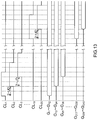
- FIG. 13 is a time chart showing the delayed clock signals CL generated when the delay time designation signal DT 1 indicates “2 ⁇ UD”, and the output timing of the pixel drive voltages G;
- FIG. 14 is a time chart showing the delayed clock signals CL generated when the delay time designation signal DT 1 indicates “3 ⁇ UD”, and the output timing of the pixel drive voltages G;
- FIG. 15 is a time chart showing the delayed clock signals CL generated when the delay time designation signal DT 1 indicates “4 ⁇ UD”, and the output timing of the pixel drive voltages G;
- FIG. 16 illustrates a delay form of pixel drive voltages G 1 to G 960 supplied to the display device 20 by the data driver 13 when the delay time designation signals DT 1 and DT 4 indicate “2 ⁇ UD” and DT 2 and DT 3 indicate “3 ⁇ UD”;
- FIG. 17 illustrates a delay form of the pixel drive voltages G 1 to G 960 supplied to the display device 20 by the data driver 13 when the delay time designation signals DT 1 and DT 4 indicate “UD” and DT 2 and DT 3 indicate “4 ⁇ UD”;
- FIG. 18 illustrates one example of the delay form of the pixel drive voltage G 1 to G 960 supplied to the display device 20 by the data driver 13 when only a scanning driver 12 A, out of the scanning drivers 12 A and 12 B, is connected to horizontal scan lines S 1 to S m ;
- FIG. 19 illustrates one example of the delay form of the pixel drive voltage G 1 to G 960 supplied to the display device 20 by the data driver 13 when only the scanning driver 12 B, out of the scanning drivers 12 A and 12 B, is connected to the horizontal scan lines S 1 to S m ;
- FIG. 20 is a circuit diagram illustrating the configuration of shift registers (SR 1 to SR 4 ) which can change a shift direction;
- FIG. 21 illustrates another example of the delay form of the pixel drive voltages G 1 to G 960 supplied to the display device 20 by the data driver 13 that incorporates the shift registers which can change the shift direction;
- FIG. 22 illustrates another example of the delay form of the pixel drive voltages G 1 to G 960 supplied to the display device 20 by the data driver 13 that incorporates the shift registers which can change the shift direction.
- FIG. 1 is a schematic configuration view of a display apparatus 100 including a display device driver according to the present invention.
- the display device 20 is made of a liquid crystal or an organic EL panel, for example.
- the display device 20 has m (m is a natural number of 2 or more) horizontal scan lines S 1 to S m formed to extend in a horizontal direction on a two-dimensional screen and n (n is a natural number of 2 or more) data lines D 1 to D n formed to extend in a perpendicular direction on the two-dimensional screen.
- a display cell that serves as a pixel is formed in each crossing portion between the horizontal scan lines and the data lines.
- the drive controller 11 detects a horizontal synchronization signal in a video signal VD, and supplies the horizontal synchronization signal HS to the scanning drivers 12 A and 12 B.
- the drive controller 11 also generates, on the basis of the video signal VD, a sequence of pixel data PD indicative of a luminance level of each pixel in 8 bits, for example.
- the drive controller 11 supplies a video data signal VPS to the data driver 13 , the video data signal VPS including: the sequence of the pixel data PD; a latching timing signal LD in synchronization with a horizontal synchronization signal included in the video signal VD; and delay time designation signals DT 1 to DT 4 of four systems.
- the scanning driver 12 A is connected to one end of each of the horizontal scan lines S 1 to S m as illustrated in FIG. 1 .
- the scanning driver 12 B is connected to the other end of each of the horizontal scan lines S 1 to S m .
- the scanning drivers 12 A and 12 B generate a horizontal scanning pulse SP in synchronization with the above-stated horizontal synchronizing signal HS, and apply the horizontal scanning pulse SP to each of the horizontal scan lines S 1 to S m of the display device 20 in sequence.
- the data driver 13 latches the sequence of pixel data PD included in the video data signal VPS. Whenever the pixel data PD for one horizontal scan line, i.e., n pieces of pixel data PD, are latched, the data driver 13 converts the latched n pieces of pixel data PD into pixel drive voltages having voltage values corresponding to the luminance levels indicated by the respective pieces of pixel data PD, and applies the pixel drive voltages to the data lines D 1 to D n of the display device 20 .
- the data driver 13 is formed on a single semiconductor chip.
- FIG. 2 is a block diagram illustrating one example of the internal configuration of the data driver 13 .
- FIG. 2 illustrates the configuration of the data driver 13 in the case where, for example, the number of the data lines D in the display device 20 , i.e., the value of “n”, is 960.
- a video data reception unit 130 sequentially latches pieces of the pixel data PD corresponding to the respective pixels from the video data signal VPS supplied from the drive controller 11 . Whenever the pixel data PD for one horizontal scan line, i.e., 960 pieces of pixel data PD, are latched, the video data reception unit 130 supplies the latched 960 pieces of pixel data PD to the first data latch unit 131 as pixel data P 1 to P 960 . The video data reception unit 130 further extracts a latching timing signal LD and delay time designation signals DT 1 to DT 4 from the video data signal VPS, and supplies each signal to the delay controller 132 .
- the first data latch unit 131 latches the pixel data P 1 to P 960 supplied from the video data reception unit 130 , and supplies the pixel data pieces to a subsequent second data latch unit 133 as pixel data R 1 to R 960 , respectively.
- the delay controller 132 generates delayed clock signals CL 1 to CL 80 on the basis of the latching timing signal LD and the delay time designation signals DT 1 to DT 4 .
- the delayed clock signals CL 1 to CL 80 causes the pixel drive voltages to be output at timing which is different between four groups.
- the delay controller 132 supplies these signals to the second data latch unit 133 .
- the configuration and detailed operation of the delay controller 132 will be described later.
- the second data latch unit 133 latches the pixel data R 1 to R 960 supplied from the first data latch unit 131 , twelve pieces at a time, in synchronization with the respective delayed clock signals CL 1 to CL 80 .
- the second data latch unit 133 supplies, at the timing of latching, the pieces of data to a gradation voltage converter 134 as pixel data Y 1 to Y 960 , respectively.
- FIG. 3 is a circuit diagram illustrating one example of the internal configuration of the second data latch unit 133 .
- the second data latch unit 133 includes latching groups L 1 to L 80 corresponding to the delayed clock signals CL 1 to CL 80 , respectively.
- the latching groups L 1 to L 80 each latch twelve pieces of pixel data R in response to a delayed clock signal CL corresponding to the latching group L.
- the latching groups L 1 to L 80 then supplies the latched pixel data R to the gradation voltage converter 134 as the pixel data Y 1 to Y 960 at the timing of latching.
- the latching group L 1 of the second data latch unit 133 latches pixel data R 1 to R 12 , out of the pixel data R 1 to R 960 , in response to the delayed clock signal CL 1 .
- the latching group L 1 supplies the pixel data pieces to the gradation voltage converter 134 as pixel data Y 1 to Y 12 , respectively.
- the latching group L 2 latches pixel data R 13 to R 24 , out of the pixel data R 1 to R 960 , in response to the delayed clock signal CL 2 .
- the latching group L 2 supplies the pixel data pieces to the gradation voltage converter 134 as pixel data Y 13 to Y 24 , respectively.
- the latching group L 3 latches pixel data R 25 to R 36 , out of the pixel data R 1 to R 960 , in response to the delayed clock signal CL 3 .
- the latching group L 3 supplies the pixel data pieces to the gradation voltage converter 134 as pixel data Y 25 to Y 36 , respectively.
- the latching group L 79 latches pixel data R 937 to R 948 , out of the pixel data R 1 to R 960 , in response to the delayed clock signal CL 79 .
- the latching group L 79 supplies the pixel data pieces to the gradation voltage converter 134 as pixel data Y 937 to Y 948 , respectively.
- the latching group L 80 latches pixel data R 949 to R 960 , out of the pixel data R 1 to R 960 , in response to the delayed clock signal CL 80 .
- the latching group L 80 supplies the pixel data pieces to the gradation voltage converter 134 as pixel data Y 949 to Y 960 , respectively.
- the gradation voltage converter 134 converts the pixel data Y 1 to Y 960 supplied from the second data latch unit 133 into pixel gradation voltages V 1 to V 960 having voltage values corresponding to the luminance levels of the respective pixels, and supplies the gradation voltages to the output amplifier unit 135 .
- the output amplifier unit 135 amplifies each of the pixel drive voltages V 1 to V 960 to obtain pixel drive voltages G 1 to G 960 having respective desired values, and applies the amplified pixel drive voltages G 1 to G 960 to data lines D 1 to D 960 of the display device 20 , respectively.
- the data driver 13 converts the pixel data R 1 to R 960 into pixel drive voltages G 1 to G 960 , where the pixel data R 1 to R 960 are indicative of the luminance levels of the respective pixels based on a video signal, and the pixel drive voltages G 1 to G 960 have voltage values corresponding to the luminance levels, respectively.
- the data driver 13 then sequentially delays each of these pixel drive voltages G 1 to G 960 in response to the delayed clock signals CL 1 to CL 80 generated based on the delay time designated by the delay time designation signals DT 1 to DT 4 .
- the data driver 13 then applies the delayed pixel drive voltages G 1 to G 960 to the data line D 1 to D 960 of the display device 20 .
- FIG. 4 is a block diagram illustrating the internal configuration of the delay controller 132 .
- a reference clock generating unit 320 generates reference clock signals CLK 1 to CLK 5 of five systems illustrated in FIG. 5 in response to the latching timing signal LD.
- the reference clock signals CLK 1 to CLK 5 are identical in frequency and different in phase of a rising edge portion. More specifically, the reference clock generating unit 320 first generates a reference clock signal CLK 1 in synchronization with the latching timing signal LD.
- the reference clock generating unit 320 further generates a signal delayed by unit delay time UD from the reference clock signal CLK 1 as a reference clock signal CLK 2 , and generates a signal delayed by the unit delay time UD from the reference clock signal CLK 2 as a reference clock signal CLK 3 .
- the reference clock generating unit 320 also generates a signal delayed by the unit delay time UD from the reference clock signal CLK 3 as a reference clock signal CLK 4 , and generates a signal delayed by the unit delay time UD from the reference clock signal CLK 4 as a reference clock signal CLK 5 .
- the unit delay time UD is set so that a phase difference between the reference clock signals CLK 5 and CLK 1 is equal to the unit delay time UD.
- the reference clock generating unit 320 supplies the reference clock signals CLK 1 to CLK 5 illustrated in FIG. 5 to delayed clock generation units 321 to 324 .
- the delayed clock generation unit 321 generates delayed clock signals CL 1 to CL 20 on the basis of the latching timing signal LD and the reference clock signals CL 1 to CL 5 .
- the delayed clock signals CL 1 to CL 20 are formed so that the timing of the respective edge portions is sequentially delayed by the delay time designated by the delay time designation signal DT 1 as illustrated in FIG. 6 .
- the delayed clock generation unit 321 supplies the delayed clock signals CL 1 to CL 20 to the second data latch unit 133 .
- the delayed clock generation unit 321 further sends out the latching timing signal LD as latching timing signal LD N to the delayed clock generation unit 322 at the timing of the delayed clock signal CL 20 illustrated in FIG. 6 .
- the delayed clock generation unit 322 generates delayed clock signals CL 21 to CL 40 on the basis of the latching timing signal LD N and the reference clock signals CLK 1 to CLK 5 .
- the delayed clock signals CL 21 to CL 40 are formed so that the timing of the respective rising edges is sequentially delayed by the delay time designated by a delay time designation signal DT 2 .
- the delayed clock generation unit 322 supplies the delayed clock signals CL 21 to CL 40 to the second data latch unit 133 .
- the delayed clock generation unit 323 generates delayed clock signals CL 60 to CL 41 on the basis of the latching timing signal LD N and the reference clock signals CLK 1 to CLK 5 supplied from the delayed clock generation unit 324 .
- the delayed clock signals CL 60 to CL 41 are formed so that the timing of the respective rising edges is sequentially delayed by the delay time designated by a delay time designation signal DT 3 as illustrated in FIG. 6 .
- the delayed clock generation unit 323 supplies the delayed clock signals CL 60 to CL 41 to the second data latch unit 133 .
- the delayed clock generation unit 324 generates delayed clock signals CL 80 to CL 61 on the basis of the latching timing signal LD and the reference clock signals CLK 1 to CLK 5 .
- the delayed clock signals CL 80 to CL 61 are formed so that the timing of the respective rising edges is sequentially delayed by the delay time designated by a delay time designation signal DT 4 as illustrated in FIG. 6 .
- the delayed clock generation unit 324 supplies the delayed clock signals CL 80 to CL 61 to the second data latch unit 133 .
- the delayed clock generation unit 324 further sends out the latching timing signal LD as latching timing signal LD N to the delayed clock generation unit 323 at the timing of the delayed clock signal CL 61 .
- the delay time designation signals DT 1 to DT 4 correspond to the pixel drive voltages G 1 to G 240 belonging to a first group, the pixel drive voltages G 241 to G 480 belonging to a second group, the pixel drive voltages G 481 to G 720 belonging to a third group, and the pixel drive voltages G 721 to G 960 belonging to a fourth group in the pixel drive voltages G 1 to G 960 , respectively.
- the delay time designation signal DT 1 is a signal for designating the delay time to sequentially delay and output the pixel drive voltages G 1 to G 240 belonging to the first group in units of twelve voltages, for example.
- the delay time designation signal DT 2 is a signal for designating the delay time to sequentially delay and output the pixel drive voltages G 241 to G 480 belonging to the second group in units of twelve voltages, for example.
- the delay time designation signal DT 3 is a signal for designating the delay time to sequentially delay and output the pixel drive voltages G 481 to G 720 belonging to the third group in units of twelve voltages, for example.
- the delay time designation signal DT 4 is a signal for designating the delay time to sequentially delay and output the pixel drive voltages G 721 to G 960 belonging to the fourth group in units of twelve voltages, for example.
- the delayed clock generation units 321 to 324 have an identical internal configuration.
- FIG. 7 is a circuit diagram illustrating the internal configuration of the delayed clock generation unit 321 selected out of the delayed clock generation units 321 to 324 .
- a delay time register RG latches the delay time designation signal DT 1 , and supplies to a clock switch unit CSC a clock allocation signal corresponding to the delay time designated in the DT 1 .
- the delay time designation signal DT 1 designates any one delay time out of, for example, the above-stated unit delay time “UD”, “2 ⁇ UD”, “3 ⁇ UD”, and “4 ⁇ UD” as delay time.
- the delay time designation signals DT 2 to DT 4 designate any one delay time out of the delay time “UD”, “2 ⁇ UD”, “3 ⁇ UD”, and “4 ⁇ UD” as in the case of the DT 1 .
- the clock switch unit CSC of the delayed clock generation unit 321 sends out the reference clock signals CLK 1 to CLK 5 having the following correspondence relation to the clock lines SL 1 to SL 5 as shift clocks SCK 1 to SCK 5 , respectively.
- the clock switch unit CSC sends out the reference clock signals CLK 1 to CLK 5 having the following correspondence relation to the clock lines SL 1 to SL 5 as the shift clocks SCK 1 to SCK 5 , when the delay time designation signal DT 1 indicates “UD”:
- the clock switch unit CSC supplies the shift clocks SCK 1 to SCK 5 illustrated in FIG. 8 to the shift registers SR 1 to SR 4 .
- the clock switch unit CSC also sends out the reference clock signals CLK 1 to CLK 5 having the following correspondence relation to the clock lines SL 1 to SL 5 as the shift clocks SCK 1 to SCK 5 , when the delay time designation signal DT 1 indicates “2 ⁇ UD”:
- the clock switch unit CSC supplies the shift clocks SCK 1 to SCK 5 illustrated in FIG. 9 to the shift registers SR 1 to SR 4 .
- the clock switch unit CSC also sends out the reference clock signals CLK 1 to CLK 5 having the following correspondence relation to the clock lines SL 1 to SL 5 as the shift clocks SCK 1 to SCK 5 when the delay time designation signal DT 1 indicates “3 ⁇ UD”:
- the clock switch unit CSC supplies the shift clocks SCK 1 to SCK 5 illustrated in FIG. 10 to the shift registers SR 1 to SR 4 .
- the clock switch unit CSC also sends out the reference clock signals CLK 1 to CLK 5 having the following correspondence relation to the clock lines SL 1 to SL 5 as the shift clocks SCK 1 to SCK 5 , when the delay time designation signal DT 1 indicates “4 ⁇ UD”:
- the clock switch unit CSC supplies the shift clocks SCK 1 to SCK 5 illustrated in FIG. 11 to the shift registers SR 1 to SR 4 .
- the shift registers SR 1 to SR 4 are connected in cascade, and their internal configuration is identical. That is, the shift registers SR 1 to SR 4 each include flip-flops F 1 to F 5 which are connected in cascade.
- the latching timing signal LD is supplied to a data terminal of the top flip-flop F 1 in the shift register SR 1 .
- An output terminal of the last flip-flop F 5 in the SR 1 is connected to a data terminal of the top flip-flop F 1 in the shift register SR 2 .
- An output terminal of the last flip-flop F 5 in the shift register SR 2 is connected to a data terminal of the top flip-flop F 1 in the shift register SR 3 .
- An output terminal of the last flip-flop F 5 in the SR 3 is connected to a data terminal of the top flip-flop F 1 in the shift register SR 4 .
- This configuration makes the shift registers SR 1 to SR 4 function as a 20-stage shift register including 20 cascade-connected flip-flops, each of which shifts the latching timing signal LD to its subsequent stage.
- the shift clock SCK 1 is supplied to a clock terminal of the flip-flop F 1 in each of the shift registers SR 1 to SR 4 through the clock line SL 1 .
- the shift clock SCK 2 is supplied to a clock terminal of the flip-flop F 2 in each of the shift registers SR 1 to SR 4 through the clock line SL 2 .
- the shift clock SCK 3 is supplied to a clock terminal of the flip-flop F 3 in each of the shift registers SR 1 to SR 4 through the clock line SL 3 .
- the shift clock SCK 4 is supplied to a clock terminal of the flip-flop F 4 in each of the shift registers SR 1 to SR 4 through the clock line SL 4 .
- the shift clock SCK 5 is supplied to a clock terminal of the flip-flop F 5 in each of the shift registers SR 1 to SR 4 through the clock line SL 5 .
- signals output from the respective flip-flops F 1 to F 5 in the shift register SR 1 are output as delayed clock signals CL 1 to CL 5
- signals output from the respective flip-flops F 1 to F 5 in the shift register SR 2 are output as delayed clock signals CL 6 to CL 10
- signals output from the respective flip-flops F 1 to F 5 in the shift register SR 3 are output as delayed clock signals CL 11 to CL 15
- signals output from the respective flip-flops F 1 to F 5 in the shift register SR 4 are output as delayed clock signals CL 16 to CL 20 .
- the latching timing signal LD N is output from the output terminal of the last flip-flop F 5 in the shift register SR 4 .
- signals output from the respective flip-flops F 1 to F 5 in the shift register SR 1 are output as delayed clock signals CL 21 to CL 25
- signals output from the respective flip-flops F 1 to F 5 in the shift register SR 2 are output as delayed clock signals CL 26 to CL 30
- signals output from the respective flip-flops F 1 to F 5 in the shift register SR 3 are output as delayed clock signals CL 31 to CL 35
- signals output from the respective flip-flops F 1 to F 5 in the shift register SR 4 are output as delayed clock signals CL 36 to CL 40 .
- signals output from the respective flip-flops F 1 to F 5 in the shift register SR 1 are output as delayed clock signals CL 60 to CL 56
- signals output from the respective flip-flops F 1 to F 5 in the shift register SR 2 are output as delayed clock signals CL 55 to CL 51
- signals output from the respective flip-flops F 1 to F 5 in the shift register SR 3 are output as delayed clock signals CL 50 to CL 46
- signals output from the respective flip-flops F 1 to F 5 in the shift register SR 4 are output as delayed clock signals CL 45 to CL 41 .
- signals output from the respective flip-flops F 1 to F 5 in the shift register SR 1 are output as delayed clock signals CL 80 to CL 76
- signals output from the respective flip-flops F 1 to F 5 in the shift register SR 2 are output as delayed clock signals CL 75 to CL 71
- signals output from the respective flip-flops F 1 to F 5 in the shift register SR 3 are output as delayed clock signals CL 70 to CL 66
- signals output from the respective flip-flops F 1 to F 5 in the shift register SR 4 are output as delayed clock signals CL 65 to CL 61 .
- the latching timing signal LD N is output from the output terminal of the last flip-flop F 5 in the shift register SR 4 .
- the delayed clock generation unit 321 when a delay time designation signal DT 1 that designates “UD” as delay time is supplied, the delayed clock generation unit 321 generates delayed clock signals CL 1 to CL 20 having rising edges sequentially delayed by the unit delay time UD as illustrated in FIG. 12 .
- the delayed clock generation unit 321 then supplies the generated signals to the second data latch unit 133 .
- latching groups L 1 to L 20 in the second data latch unit 133 latch pixel data R 1 to R 240 supplied from the first data latch unit 131 , twelve data pieces at a time, at the timing corresponding to the delayed clock signals CL 1 to CL 20 , respectively.
- the latching groups L 1 to L 20 then supply the respective data pieces to the gradation voltage converter 134 as pixel data Y 1 to Y 240 at the timing of latching the data pieces.
- the gradation voltage converter 134 and the output amplifier unit 135 sequentially supply the respective pixel drive voltages G 1 to G 240 based on the respective pixel data Y 1 to Y 240 , at the timing sequentially delayed in units of twelve voltages by the unit delay time UD as illustrated in FIG. 12 .
- the delayed clock generation unit 321 when a delay time designation signal DT 1 that designates “2 ⁇ UD” as delay time is supplied, the delayed clock generation unit 321 generates delayed clock signals CL 1 to CL 20 having rising edge portions sequentially delayed by 2 ⁇ UD as illustrated in FIG. 13 .
- the delayed clock generation unit 321 then supplies the generated signals to the second data latch unit 133 .
- the latching groups L 1 to L 20 in the second data latch unit 133 latch pixel data R 1 to R 240 supplied from the first data latch unit 131 , twelve data pieces at a time, at the timing corresponding to the delayed clock signals CL 1 to CL 20 , respectively.
- the latching groups L 1 to L 20 then supply the respective data pieces to the gradation voltage converter 134 as pixel data Y 1 to Y 240 at the timing of latching the data pieces.
- the gradation voltage converter 134 and the output amplifier unit 135 supply the respective pixel drive voltages G 1 to G 240 based on the respective pixel data Y 1 to Y 240 at the timing sequentially delayed in units of twelve voltages by 2 ⁇ UD as illustrated in FIG. 13 .
- the delayed clock generation unit 321 when a delay time designation signal DT 1 that designates “3 ⁇ UD” as delay time is supplied, the delayed clock generation unit 321 generates delayed clock signals CL 1 to CL 20 having rising edge portions sequentially delayed by 3 ⁇ UD as illustrated in FIG. 14 .
- the delayed clock generation unit 321 then supplies the generated signals to the second data latch unit 133 .
- the latching groups L 1 to L 20 in the second data latch unit 133 latch pixel data R 1 to R 240 supplied from the first data latch unit 131 , twelve data pieces at a time, at the timing corresponding to the delayed clock signals CL 1 to CL 20 , respectively.
- the latching groups L 1 to L 20 then supply the respective data pieces to the gradation voltage converter 134 as pixel data Y 1 to Y 240 at the timing of latching the data pieces.
- the gradation voltage converter 134 and the output amplifier unit 135 supply pixel drive voltages G 1 to G 240 based on the respective pixel data Y 1 to Y 240 , at the timing delayed in units of twelve voltages by 3 ⁇ UD as illustrated in FIG. 14 .
- the delayed clock generation unit 321 when a delay time designation signal DT 1 is supplied to designate “4 ⁇ UD” as the delay time, the delayed clock generation unit 321 generates delayed clock signals CL 1 to CL 20 having rising edge portions sequentially delayed by 4 ⁇ UD as illustrated in FIG. 15 .
- the delayed clock generation unit 321 then supplies the generated signals to the second data latch unit 133 .
- the latching groups L 1 to L 20 in the second data latch unit 133 latches pixel data R 1 to R 240 supplied from the first data latch unit 131 , twelve data pieces at a time, at the timing corresponding to the delayed clock signals CL 1 to CL 20 , respectively.
- the latching groups L 1 to L 20 then supply the respective data pieces to the gradation voltage converter 134 as pixel data Y 1 to Y 240 at the timing of latching the data pieces.
- the gradation voltage converter 134 and the output amplifier unit 135 supply the pixel drive voltages G 1 to G 240 based on the respective pixel data Y 1 to Y 240 , at the timing delayed in units of twelve voltages by 4 ⁇ UD as illustrated in FIG. 15 .
- the delayed clock generation unit 321 changes the delay time in four stages (UD, 2 ⁇ UD, 3 ⁇ UD, 4 ⁇ UD) in response to the delay time designation signal DT 1 , the delay time being used to delay and output the pixel drive voltages G 1 to G 240 belonging to the first group, out of the pixel drive voltages G 1 to G 960 .
- the delayed clock generation unit 322 also changes the delay time in four stages in response to the delay time designation signal DT 2 , the delay time being used to delay and output the pixel drive voltages G 241 to G 480 belonging to the second group.
- the delayed clock generation unit 323 changes the delay time in four stages in response to the delay time designation signal DT 3 , the delay time being used to delay and output the pixel voltages G 481 to G 720 belonging to the third group.
- the delayed clock generation unit 324 changes the delay time in four stages in response to the delay time designation signal DT 4 , the delay time being used to delay and output the pixel voltages G 721 to G 960 belonging to the fourth group.
- FIG. 16 illustrates a delay form of the pixel drive voltages G 1 to G 960 supplied to the display device 20 when the delay time designation signals DT 1 and DT 4 indicate “2 ⁇ UD” and DT 2 and DT 3 indicate “3 ⁇ UD” as the delay time designation signals DT 1 to DT 4 .
- FIG. 17 illustrates a delay form of the pixel drive voltages G 1 to G 960 supplied to the display device 20 when the delay time designation signals DT 1 and DT 4 indicate “UD” and DT 2 and DT 3 indicate “4 ⁇ UD” as the delay time designation signals DT 1 to DT 4 .
- the delay time for each of the groups is adjusted in accordance with manufacturing variations, screen sizes, or various specifications of display devices, the timing of a scanning pulse arriving at each pixel can be made coincide with the timing of application of each pixel drive voltage. Therefore, according to the present invention, it becomes possible to display a favorable image free from uneven color.
- the pixel drive voltages G 1 to G 960 that are applied to the data lines D 1 to D 960 of the display device 20 are constituted by four groups so that the delay time of each group can be changed separately.
- the number of groups set for changing the delay time is not limited to four.
- a plurality of pixel drive voltages for one horizontal scan line may be constituted by two, eight, or sixteen groups, and the delayed clock generation unit having the configuration illustrated in FIG. 7 may be provided for each group.
- the pixel drive voltages G 1 to G 960 are supplied to the display device 20 at the timing delayed in units of twelve voltages.
- the pixel drive voltages G 1 to G 960 may be supplied to the display device 20 at the timing delayed one after another or delayed sequentially in units of two or more voltages.
- the delayed clock generation unit illustrated in FIG. 7 generates a plurality of delay clock signals (CL) by supplying reference clock signals (CLK 1 to CLK 5 ) of five systems, which are different in phase, to the clock terminals of the flip-flops in the shift registers (SR 1 to SR 4 ), respectively.
- the delayed clock generation unit changes delay time of the delay clock (CL) by changing allocation of the reference clock signals supplied to the respective flip-flops on the basis of the delay time designation signals (DT 1 to DT 4 ).
- the delayed clock generation unit may adopt the configuration in which the delay time of the delay clocks is changed by selecting one clock signal, out of a plurality of clock signals different in oscillating frequency from each other, and commonly supplying the selected clock signal to the clock terminals of the respective flip-flops of the shift registers (SR 1 to SR 4 ).
- the data driver 13 may include the delay controller ( 132 ) and the pixel drive voltage application unit (including the second data latch unit 133 , the gradation voltage converter 134 , and the output amplifier 135 ) as described below. That is, the pixel drive voltage application unit ( 132 to 135 ) converts a plurality of pixel data pieces into a plurality of pixel drive voltages (G), where the pixel data pieces represent luminance levels of respective pixels based on a video signal, and the pixel drive voltages (G) have voltage values corresponding to the luminance levels. The pixel drive voltage application unit ( 132 to 135 ) applies the converted pixel drive voltages to the display device ( 20 ).
- the delay controller ( 132 ) controls the pixel drive voltage application unit so as to cause the pixel drive voltage application unit to apply the plurality of pixel drive voltages to the display device, the plurality of pixel drive voltages being constituted by a plurality of groups and being sequentially delayed in units of the groups, the groups each including t (t is an integer greater than or equal to 2) pixel drive voltages. Furthermore, the delay controller ( 132 ) sets delay time (UD, 2 ⁇ UD, 3 ⁇ UD, and 4 ⁇ UD) designated by the delay time designation signals (DT 1 to DT 4 ) as delay time to delay each of the pixel drive voltages.
- two scanning drivers 12 A and 12 B are provided as a scanning driver for supplying horizontal scanning pulse SP to the horizontal scan lines S 1 to S m of the display device 20 , the scanning drivers 12 A and 12 B being connected to respective ends of each of the horizontal scan lines S 1 to S m .
- the scanning drivers 12 A and 12 B may be connected to one end of each of the horizontal scan lines S 1 to S m .
- the data driver 13 when only the scanning driver 12 A out of the scanning drivers 12 A and 12 B is connected to the horizontal scan lines S 1 to S m , the data driver 13 preferably supplies the pixel drive voltages G 1 to G 960 to the display device 20 in the delay form illustrated in FIG. 18 .
- the data driver 13 When only the scanning driver 12 B out of the scanning drivers 12 A and 12 B is connected to the horizontal scan lines S 1 to S m , the data driver 13 preferably supplies the pixel drive voltages G 1 to G 960 to the display device 20 in the delay form as illustrated in FIG. 19 .
- the shift registers SR 1 to SR 4 having the configuration illustrated in FIG. 20 are adopted.
- switches SW 1 to SW 5 are provided before the cascade-connected flip-flops F 1 to F 5 , respectively.
- the switch SW 1 selects one signal out of a latching timing signal LD (LD N ) and a signal output from the flip-flop F 5 , and supplies the selected signal to the flip-flop F 1 . More specifically, when a delay mode designation signal SMD indicative of the first delay mode is supplied, the switch SW 1 selects the latching timing signal LD (LD N ), and supplies the selected signal to the flip-flop F 1 .
- the switch SW 1 selects the signal output from the flip-flop F 5 , and supplies the signal to the flip-flop F 1 .
- the SW 2 selects the signal output from the flip-flop F 1 , and supplies the signal to the flip-flop F 2 . Contrary to this, when the delay mode designation signal SMD indicative of the second delay mode is supplied, the switch SW 2 selects a signal output from the flip-flop F 3 , and supplies the signal to the flip-flop F 2 .
- the SW 3 selects a signal output from the flip-flop F 2 , and supplies the signal to the flip-flop F 3 . Contrary to this, when the delay mode designation signal SMD indicative of the second delay mode is supplied, the switch SW 3 selects a signal output from the flip-flop F 4 , and supplies the signal to the flip-flop F 3 .
- the switch SW 4 selects a signal output from the flip-flop F 3 , and supplies the signal to the flip-flop F 4 . Contrary to this, when the delay mode designation signal SMD indicative of the second delay mode is supplied, the switch SW 4 selects a signal output from the flip-flop F 5 , and supplies the signal to the flip-flop F 4 .
- the switch SW 5 selects a signal output from the flip-flop F 4 , and supplies the signal to the flip-flop F 5 . Contrary to this, when the delay mode designation signal SMD indicative of the second delay mode is supplied, the switch SW 5 selects the latching timing signal LD (LD N ), and supplies the signal to the flip-flop F 5 .
- the latching timing signal LD (LD N ) is latched while being shifted to the flip-flops in order of F 1 , F 2 , F 3 , F 4 , and F 5 , when the delay mode designation signal SMD indicative of the first delay mode is supplied to a pertinent shift register.
- the pertinent shift register latches the latching timing signal LD (LD N ) while shifting the signal to the flip-flops in order of F 5 , F 4 , F 3 , F 2 , and F 1 .
- each of the delayed clock generation units 321 to 324 is equipped with a shift register that can selectively perform the first delay mode and the second delay mode as illustrated in FIG. 20 , the shift registers of the delayed clock generation units 322 and 323 are connected to each other. That is, the output terminal of the flip-flop F 5 of the shift register SR 4 in the delayed clock generation unit 322 is connected to the switch SW 1 of the shift register SR 1 in the delayed clock generation unit 323 .
- the delay controller 132 controls the pixel drive voltage application unit ( 132 to 135 ) so as to cause the pixel drive voltage application unit to apply the pixel drive voltages to the display device in the first or second delay mode designated by the delay mode designation signal (SMD) for each of the plurality of groups, the groups each including t pixel drive voltages.
- the pixel drive voltage application unit applies t pixel drive voltages included in each group to the display device, the t pixel drive voltages being delayed in order of a first pixel drive voltage, a second pixel drive voltage, . . . , a (t ⁇ 1)-th pixel drive voltage, and a t-th pixel drive voltage.
- the pixel drive voltage application unit applies t pixel drive voltages included in each group to the display device, the t pixel drive voltages being delayed in order of the t-th pixel drive voltage, the (t ⁇ 1)-th pixel drive voltage, . . . , the second pixel drive voltage, and the first pixel drive voltage, the order being reversal of the order in the first delay mode.
- the delay mode designation signal SMD indicative of the first delay mode is supplied to the delayed clock generation unit 321 corresponding to the pixel drive voltages G 1 to G 240 included in the first group, and to the delayed clock generation unit 322 corresponding to the pixel drive voltages G 241 to G 480 included in the second group.
- the shift registers SR 1 to SR 4 formed in each of the delayed clock generation units 321 and 322 operate in the above-stated first delay mode.
- the delay mode designation signal SMD indicative of the second delay mode is supplied to the delayed clock generation unit 323 corresponding to the pixel drive voltages G 481 to G 720 included in the third group, and to the delayed clock generation unit 324 corresponding to the pixel drive voltages G 721 to G 960 included in the fourth group.
- the shift registers SR 1 to SR 4 formed in each of the delayed clock generation units 323 and 324 operate in the above-stated second delay mode.
- the pixel drive voltage application unit ( 132 to 135 ) applies the pixel drive voltages G 1 to G 960 to the display device 20 in the delay form illustrated in FIG. 18 .
- the delay mode designation signal SMD indicative of the second delay mode is supplied to the delayed clock generation unit 321 corresponding to the pixel drive voltages G 1 to G 240 included in the first group, and to the delayed clock generation unit 322 corresponding to the pixel drive voltages G 241 to G 480 included in the second group.
- the shift registers SR 1 to SR 4 formed in each of the delayed clock generation units 321 and 322 operate in the above-stated second delay mode.
- the delay mode designation signal SMD indicative of the first delay mode is supplied to the delayed clock generation unit 323 corresponding to the pixel drive voltages G 481 to G 720 included in the third group, and to the delayed clock generation unit 324 corresponding to the pixel drive voltages G 721 to G 960 included in the fourth group.
- the shift registers SR 1 to SR 4 formed in each of the delayed clock generation units 323 and 324 operate in the above-stated first delay mode.
- the pixel drive voltage application unit ( 132 to 135 ) applies the pixel drive voltages G 1 to G 960 to the display device 20 in the delay form illustrated in FIG. 19 .
- the pixel drive voltages G 1 to G 960 can be applied to the data lines D 1 to D 960 of the display device 20 in the delay form illustrated not only in FIGS. 18 and 19 but also in FIGS. 21 and 22 , for example.
Landscapes
- Engineering & Computer Science (AREA)
- Chemical & Material Sciences (AREA)
- Crystallography & Structural Chemistry (AREA)
- Physics & Mathematics (AREA)
- Computer Hardware Design (AREA)
- General Physics & Mathematics (AREA)
- Theoretical Computer Science (AREA)
- Control Of Indicators Other Than Cathode Ray Tubes (AREA)
- Liquid Crystal Display Device Control (AREA)
- Liquid Crystal (AREA)
Abstract
Description
Claims (4)
Applications Claiming Priority (2)
| Application Number | Priority Date | Filing Date | Title |
|---|---|---|---|
| JP2015138527A JP6563267B2 (en) | 2015-07-10 | 2015-07-10 | Display device driver |
| JP2015-138527 | 2015-07-10 |
Publications (2)
| Publication Number | Publication Date |
|---|---|
| US20170011703A1 US20170011703A1 (en) | 2017-01-12 |
| US10621943B2 true US10621943B2 (en) | 2020-04-14 |
Family
ID=57731273
Family Applications (1)
| Application Number | Title | Priority Date | Filing Date |
|---|---|---|---|
| US15/205,089 Expired - Fee Related US10621943B2 (en) | 2015-07-10 | 2016-07-08 | Display device driver having pixel drive voltage delay selection |
Country Status (2)
| Country | Link |
|---|---|
| US (1) | US10621943B2 (en) |
| JP (1) | JP6563267B2 (en) |
Cited By (2)
| Publication number | Priority date | Publication date | Assignee | Title |
|---|---|---|---|---|
| US20210247720A1 (en) * | 2018-06-05 | 2021-08-12 | Imec Vzw | Data Distribution for Holographic Projection |
| US11232764B2 (en) * | 2019-10-08 | 2022-01-25 | Lapis Semiconductor Co., Ltd. | Display driver and display device |
Families Citing this family (10)
| Publication number | Priority date | Publication date | Assignee | Title |
|---|---|---|---|---|
| WO2018110276A1 (en) * | 2016-12-14 | 2018-06-21 | ソニーセミコンダクタソリューションズ株式会社 | Transmission device, transmission method, and communication system |
| CN108806631A (en) * | 2018-07-06 | 2018-11-13 | 青岛海信电器股份有限公司 | A kind of drive control method, apparatus and LCD TV |
| CN112309342B (en) * | 2019-07-30 | 2023-09-26 | 拉碧斯半导体株式会社 | Display device, data driver and display controller |
| US11145269B2 (en) * | 2019-08-02 | 2021-10-12 | Sakai Display Products Corporation | Display apparatus accurately reducing display non-uniformity |
| CN112820237B (en) * | 2019-10-31 | 2022-08-26 | 京东方科技集团股份有限公司 | Electronic substrate, driving method thereof and display device |
| US11501729B2 (en) * | 2019-12-13 | 2022-11-15 | Lapis Semiconductor Co., Ltd. | Source driver that adjusts a timing of outputting of pixel data based on a length of a source line, and display device |
| KR102630609B1 (en) * | 2019-12-24 | 2024-01-26 | 엘지디스플레이 주식회사 | Display apparatus |
| KR102780214B1 (en) * | 2020-03-16 | 2025-03-17 | 삼성디스플레이 주식회사 | Data driver and display apparatus having the same |
| JP7519845B2 (en) * | 2020-08-31 | 2024-07-22 | ラピスセミコンダクタ株式会社 | Display Driver |
| JP2025124269A (en) * | 2024-02-14 | 2025-08-26 | ローム株式会社 | Display driver and display device |
Citations (9)
| Publication number | Priority date | Publication date | Assignee | Title |
|---|---|---|---|---|
| US20040189579A1 (en) * | 2003-03-28 | 2004-09-30 | Yukihiro Shimizu | Driving apparatus and display module |
| US20070152947A1 (en) * | 2005-12-22 | 2007-07-05 | Yasuhiro Tanaka | Display apparatus |
| US20080129675A1 (en) * | 2006-10-26 | 2008-06-05 | Yasuhiro Tanaka | Display device |
| JP2008262132A (en) * | 2007-04-13 | 2008-10-30 | Sharp Corp | Display drive device and display device |
| US20100123705A1 (en) * | 2008-11-20 | 2010-05-20 | Manabu Nishimizu | Operational amplifier and display panel driving device |
| US20100123704A1 (en) * | 2008-11-20 | 2010-05-20 | Manabu Nishimizu | Display panel driving apparatus |
| US20110316821A1 (en) * | 2010-06-23 | 2011-12-29 | Sharp Kabushiki Kaisha | Driving circuit, liquid crystal display apparatus and electronic information device |
| US20120242722A1 (en) * | 2011-03-24 | 2012-09-27 | Hiroaki Ishii | Display panel drive device, semiconductor integrated device, and image data acquisition method in display panel drive device |
| US20150325214A1 (en) * | 2014-05-07 | 2015-11-12 | Dongbu Hitek Co., Ltd. | Data Driver And A Display Apparatus Including The Same |
Family Cites Families (2)
| Publication number | Priority date | Publication date | Assignee | Title |
|---|---|---|---|---|
| JP4693757B2 (en) * | 2005-12-02 | 2011-06-01 | 株式会社半導体エネルギー研究所 | Display device |
| KR20130112213A (en) * | 2012-04-03 | 2013-10-14 | 삼성전자주식회사 | Display device and image data signagl outputting method thereof |
-
2015
- 2015-07-10 JP JP2015138527A patent/JP6563267B2/en not_active Expired - Fee Related
-
2016
- 2016-07-08 US US15/205,089 patent/US10621943B2/en not_active Expired - Fee Related
Patent Citations (11)
| Publication number | Priority date | Publication date | Assignee | Title |
|---|---|---|---|---|
| US20040189579A1 (en) * | 2003-03-28 | 2004-09-30 | Yukihiro Shimizu | Driving apparatus and display module |
| JP2004301946A (en) | 2003-03-28 | 2004-10-28 | Sharp Corp | Driving device and display module having the same |
| US20070152947A1 (en) * | 2005-12-22 | 2007-07-05 | Yasuhiro Tanaka | Display apparatus |
| JP2007171597A (en) | 2005-12-22 | 2007-07-05 | Hitachi Displays Ltd | Display device |
| US20080129675A1 (en) * | 2006-10-26 | 2008-06-05 | Yasuhiro Tanaka | Display device |
| JP2008262132A (en) * | 2007-04-13 | 2008-10-30 | Sharp Corp | Display drive device and display device |
| US20100123705A1 (en) * | 2008-11-20 | 2010-05-20 | Manabu Nishimizu | Operational amplifier and display panel driving device |
| US20100123704A1 (en) * | 2008-11-20 | 2010-05-20 | Manabu Nishimizu | Display panel driving apparatus |
| US20110316821A1 (en) * | 2010-06-23 | 2011-12-29 | Sharp Kabushiki Kaisha | Driving circuit, liquid crystal display apparatus and electronic information device |
| US20120242722A1 (en) * | 2011-03-24 | 2012-09-27 | Hiroaki Ishii | Display panel drive device, semiconductor integrated device, and image data acquisition method in display panel drive device |
| US20150325214A1 (en) * | 2014-05-07 | 2015-11-12 | Dongbu Hitek Co., Ltd. | Data Driver And A Display Apparatus Including The Same |
Cited By (3)
| Publication number | Priority date | Publication date | Assignee | Title |
|---|---|---|---|---|
| US20210247720A1 (en) * | 2018-06-05 | 2021-08-12 | Imec Vzw | Data Distribution for Holographic Projection |
| US11847944B2 (en) * | 2018-06-05 | 2023-12-19 | Imec Vzw | Data distribution for holographic projection |
| US11232764B2 (en) * | 2019-10-08 | 2022-01-25 | Lapis Semiconductor Co., Ltd. | Display driver and display device |
Also Published As
| Publication number | Publication date |
|---|---|
| US20170011703A1 (en) | 2017-01-12 |
| JP6563267B2 (en) | 2019-08-21 |
| JP2017021188A (en) | 2017-01-26 |
Similar Documents
| Publication | Publication Date | Title |
|---|---|---|
| US10621943B2 (en) | Display device driver having pixel drive voltage delay selection | |
| US9542902B2 (en) | Display device driver | |
| US9972265B2 (en) | Display apparatus, method of driving display panel using the same and driver for the display apparatus | |
| US8378999B2 (en) | Driving circuit and data driver of planar display device | |
| US10410595B2 (en) | Display driver | |
| US9754524B2 (en) | Display driver | |
| KR102703114B1 (en) | Display device and operation method thereof | |
| KR102199930B1 (en) | Gate driver ic and control method thereof | |
| EP3236459B1 (en) | Scanning drive circuit and display device | |
| KR102155015B1 (en) | Source driver and operating method thereof | |
| WO2019024657A1 (en) | Display device and driving method therefor | |
| US20170169754A1 (en) | Source Driver, Driving Circuit and Driving Method for TFT-LCD | |
| US20190189076A1 (en) | Source driver and display device including the same | |
| US8355032B2 (en) | Displaying apparatus, displaying panel driver and displaying panel driving method | |
| KR920010748B1 (en) | Halftone display driving circuit and halftone display method of liquid crystal matrix panel | |
| CN101034543B (en) | Display driving signal processor, display apparatus and a method of processing display driving signal | |
| US7719509B2 (en) | Driver for liquid crystal display | |
| TW201717178A (en) | Gate driving circuit | |
| JP2007041258A (en) | Image display device and timing controller | |
| KR100782306B1 (en) | Frame recognition signal generator, generating method, and apparatus having same | |
| KR102207191B1 (en) | Display Device | |
| US20260018145A1 (en) | Display driver and display device | |
| KR20190079825A (en) | GIP Driving Circuit and Display Device Using the Same | |
| JP6517651B2 (en) | Display driver | |
| KR20170064645A (en) | Display Device |
Legal Events
| Date | Code | Title | Description |
|---|---|---|---|
| AS | Assignment |
Owner name: LAPIS SEMICONDUCTOR CO., LTD., JAPAN Free format text: ASSIGNMENT OF ASSIGNORS INTEREST;ASSIGNOR:HIGUCHI, KOJI;REEL/FRAME:039106/0189 Effective date: 20160622 |
|
| STPP | Information on status: patent application and granting procedure in general |
Free format text: FINAL REJECTION MAILED |
|
| STPP | Information on status: patent application and granting procedure in general |
Free format text: DOCKETED NEW CASE - READY FOR EXAMINATION |
|
| STPP | Information on status: patent application and granting procedure in general |
Free format text: NON FINAL ACTION MAILED |
|
| STPP | Information on status: patent application and granting procedure in general |
Free format text: RESPONSE TO NON-FINAL OFFICE ACTION ENTERED AND FORWARDED TO EXAMINER |
|
| STPP | Information on status: patent application and granting procedure in general |
Free format text: NOTICE OF ALLOWANCE MAILED -- APPLICATION RECEIVED IN OFFICE OF PUBLICATIONS |
|
| STCF | Information on status: patent grant |
Free format text: PATENTED CASE |
|
| FEPP | Fee payment procedure |
Free format text: MAINTENANCE FEE REMINDER MAILED (ORIGINAL EVENT CODE: REM.); ENTITY STATUS OF PATENT OWNER: LARGE ENTITY |
|
| LAPS | Lapse for failure to pay maintenance fees |
Free format text: PATENT EXPIRED FOR FAILURE TO PAY MAINTENANCE FEES (ORIGINAL EVENT CODE: EXP.); ENTITY STATUS OF PATENT OWNER: LARGE ENTITY |
|
| STCH | Information on status: patent discontinuation |
Free format text: PATENT EXPIRED DUE TO NONPAYMENT OF MAINTENANCE FEES UNDER 37 CFR 1.362 |
|
| FP | Lapsed due to failure to pay maintenance fee |
Effective date: 20240414 |