US10609826B2 - Display apparatus having a full-thickness through hole - Google Patents
Display apparatus having a full-thickness through hole Download PDFInfo
- Publication number
- US10609826B2 US10609826B2 US15/336,944 US201615336944A US10609826B2 US 10609826 B2 US10609826 B2 US 10609826B2 US 201615336944 A US201615336944 A US 201615336944A US 10609826 B2 US10609826 B2 US 10609826B2
- Authority
- US
- United States
- Prior art keywords
- hole
- display apparatus
- layer
- organic light
- emitting display
- Prior art date
- Legal status (The legal status is an assumption and is not a legal conclusion. Google has not performed a legal analysis and makes no representation as to the accuracy of the status listed.)
- Active, expires
Links
Images


Classifications
-
- H—ELECTRICITY
- H05—ELECTRIC TECHNIQUES NOT OTHERWISE PROVIDED FOR
- H05K—PRINTED CIRCUITS; CASINGS OR CONSTRUCTIONAL DETAILS OF ELECTRIC APPARATUS; MANUFACTURE OF ASSEMBLAGES OF ELECTRICAL COMPONENTS
- H05K5/00—Casings, cabinets or drawers for electric apparatus
- H05K5/0017—Casings, cabinets or drawers for electric apparatus with operator interface units
-
- G—PHYSICS
- G09—EDUCATION; CRYPTOGRAPHY; DISPLAY; ADVERTISING; SEALS
- G09F—DISPLAYING; ADVERTISING; SIGNS; LABELS OR NAME-PLATES; SEALS
- G09F9/00—Indicating arrangements for variable information in which the information is built-up on a support by selection or combination of individual elements
- G09F9/30—Indicating arrangements for variable information in which the information is built-up on a support by selection or combination of individual elements in which the desired character or characters are formed by combining individual elements
- G09F9/33—Indicating arrangements for variable information in which the information is built-up on a support by selection or combination of individual elements in which the desired character or characters are formed by combining individual elements being semiconductor devices, e.g. diodes
-
- G—PHYSICS
- G06—COMPUTING OR CALCULATING; COUNTING
- G06F—ELECTRIC DIGITAL DATA PROCESSING
- G06F1/00—Details not covered by groups G06F3/00 - G06F13/00 and G06F21/00
- G06F1/16—Constructional details or arrangements
- G06F1/1613—Constructional details or arrangements for portable computers
- G06F1/1626—Constructional details or arrangements for portable computers with a single-body enclosure integrating a flat display, e.g. Personal Digital Assistants [PDAs]
-
- G06K9/00013—
-
- G—PHYSICS
- G06—COMPUTING OR CALCULATING; COUNTING
- G06V—IMAGE OR VIDEO RECOGNITION OR UNDERSTANDING
- G06V40/00—Recognition of biometric, human-related or animal-related patterns in image or video data
- G06V40/10—Human or animal bodies, e.g. vehicle occupants or pedestrians; Body parts, e.g. hands
- G06V40/12—Fingerprints or palmprints
- G06V40/13—Sensors therefor
-
- H01L27/323—
-
- H—ELECTRICITY
- H02—GENERATION; CONVERSION OR DISTRIBUTION OF ELECTRIC POWER
- H02J—CIRCUIT ARRANGEMENTS OR SYSTEMS FOR SUPPLYING OR DISTRIBUTING ELECTRIC POWER; SYSTEMS FOR STORING ELECTRIC ENERGY
- H02J50/00—Circuit arrangements or systems for wireless supply or distribution of electric power
- H02J50/10—Circuit arrangements or systems for wireless supply or distribution of electric power using inductive coupling
-
- H02J7/025—
-
- H—ELECTRICITY
- H04—ELECTRIC COMMUNICATION TECHNIQUE
- H04M—TELEPHONIC COMMUNICATION
- H04M1/00—Substation equipment, e.g. for use by subscribers
- H04M1/02—Constructional features of telephone sets
- H04M1/0202—Portable telephone sets, e.g. cordless phones, mobile phones or bar type handsets
-
- H—ELECTRICITY
- H10—SEMICONDUCTOR DEVICES; ELECTRIC SOLID-STATE DEVICES NOT OTHERWISE PROVIDED FOR
- H10K—ORGANIC ELECTRIC SOLID-STATE DEVICES
- H10K59/00—Integrated devices, or assemblies of multiple devices, comprising at least one organic light-emitting element covered by group H10K50/00
- H10K59/40—OLEDs integrated with touch screens
-
- H—ELECTRICITY
- H10—SEMICONDUCTOR DEVICES; ELECTRIC SOLID-STATE DEVICES NOT OTHERWISE PROVIDED FOR
- H10K—ORGANIC ELECTRIC SOLID-STATE DEVICES
- H10K59/00—Integrated devices, or assemblies of multiple devices, comprising at least one organic light-emitting element covered by group H10K50/00
- H10K59/80—Constructional details
- H10K59/87—Passivation; Containers; Encapsulations
-
- G—PHYSICS
- G06—COMPUTING OR CALCULATING; COUNTING
- G06F—ELECTRIC DIGITAL DATA PROCESSING
- G06F2203/00—Indexing scheme relating to G06F3/00 - G06F3/048
- G06F2203/041—Indexing scheme relating to G06F3/041 - G06F3/045
- G06F2203/04105—Pressure sensors for measuring the pressure or force exerted on the touch surface without providing the touch position
-
- H—ELECTRICITY
- H04—ELECTRIC COMMUNICATION TECHNIQUE
- H04M—TELEPHONIC COMMUNICATION
- H04M1/00—Substation equipment, e.g. for use by subscribers
- H04M1/02—Constructional features of telephone sets
- H04M1/0202—Portable telephone sets, e.g. cordless phones, mobile phones or bar type handsets
- H04M1/026—Details of the structure or mounting of specific components
- H04M1/0266—Details of the structure or mounting of specific components for a display module assembly
-
- H—ELECTRICITY
- H04—ELECTRIC COMMUNICATION TECHNIQUE
- H04M—TELEPHONIC COMMUNICATION
- H04M1/00—Substation equipment, e.g. for use by subscribers
- H04M1/02—Constructional features of telephone sets
- H04M1/0202—Portable telephone sets, e.g. cordless phones, mobile phones or bar type handsets
- H04M1/0279—Improving the user comfort or ergonomics
-
- H—ELECTRICITY
- H10—SEMICONDUCTOR DEVICES; ELECTRIC SOLID-STATE DEVICES NOT OTHERWISE PROVIDED FOR
- H10K—ORGANIC ELECTRIC SOLID-STATE DEVICES
- H10K77/00—Constructional details of devices covered by this subclass and not covered by groups H10K10/80, H10K30/80, H10K50/80 or H10K59/80
Definitions
- One or more embodiments relate to a display apparatus, and more particularly, to a display apparatus having a full-thickness through hole.
- Portable display apparatuses often make use of a planar large screen display that is capable of displaying a large amount of information at the same time.
- Examples of apparatuses that include a large screen display unit include a portable phone, a tablet PC, or a portable game console.
- planar large screen display devices frequently render the portable apparatus incorporating the display difficult to grip with one hand, and accordingly, the portable apparatus having the large-screen display may be easily dropped from the hand.
- One or more exemplary embodiments of the present invention include a display apparatus and an organic light-emitting display apparatus with a developed grip, the display apparatus being capable of providing various additional functions in addition to displaying large amounts of information at the same time.
- a display apparatus includes a display panel including a plurality of display pixels.
- a cover layer is located over a first surface of the display panel on which an image is displayed.
- a housing is located over a second surface of the display panel, the second surface being opposite to the first surface of the display panel. At least one through hole linearly penetrates the display panel, the cover layer, and the housing.
- the at least one through hole may pass through an area of the display panel on which an image is displayed.
- the at least one through hole may pass through an area of the display panel on which no image is displayed.
- a smallest diameter of the at least one through hole may be about 10 mm or more and about 100 mm or less.
- a structure that separates an outer portion of the display apparatus and an inner portion of the at least one through hole from each other might not be installed in the cover layer and the housing that are on a path that linearly penetrates the at least one through hole.
- the at least one through hole may include a first through hole passing through the cover layer.
- a second through hole may pass through the display panel.
- a third through hole may pass through the housing.
- Diameters of inner circumferential surfaces of the first through hole, the second through hole, and the third through hole may be substantially the same.
- the display apparatus may further include a signal input element disposed in an area adjacent to the at least one through hole.
- the signal input element may be located over a sidewall of an inner circumferential surface of the at least one through hole, in an upper outline area of the at least one through hole near the first surface of the display panel, and/or in a lower outline area of the at least one through hole near the second surface of the display panel.
- the display apparatus may further include a signal sensing element disposed in an area adjacent to the at least one through hole.
- the signal sensing element may be located at over a sidewall of an inner circumferential surface of the at least one through hole, in an upper outline area of the at least one through hole near the first surface of the display panel, and/or in a lower outline area of the at least one through hole near the second surface of the display panel.
- the display apparatus may further include a wireless charging connection terminal disposed over a sidewall of an inner circumferential sidewall of the at least one through hole.
- the display apparatus may further include an insulator disposed between the inner circumferential surface of the at least one through hole and the wireless charging connection terminal.
- an organic light-emitting display apparatus includes a housing.
- a substrate is disposed over the housing.
- An organic light-emitting display layer is disposed over the substrate.
- An encapsulation layer encapsulates the organic light-emitting display layer.
- a transparent cover layer is disposed over the encapsulating layer. At least one through hole linearly penetrates the substrate, the organic light-emitting display layer, the encapsulating layer, the transparent cover layer, and the housing.
- a side surface of the organic light-emitting display layer adjacent to an inner circumferential surface of the at least one through hole is surrounded by the encapsulating layer.
- the substrate may include a flexible substrate.
- the encapsulating layer may include at least one organic layer and at least one inorganic layer.
- a side surface of the organic light-emitting display layer may be surrounded by the at least one inorganic layer.
- the organic light-emitting display apparatus may further include a signal input element,
- the signal input element may include a button, a wheel, and/or a switch.
- the organic light-emitting display apparatus may further include a signal sensing element.
- the signal sensing element may include an optical sensor, a tactile sensor, a pressure sensor, and/or a fingerprint recognition sensor.
- the organic light-emitting display apparatus may further include a wireless charging connection terminal disposed over a sidewall of an inner circumferential surface of the at least one through hole.
- the organic light-emitting display apparatus may further include an insulator covering the wireless charging connection terminal.
- FIG. 1 is a schematic perspective view of a display apparatus according to an exemplary embodiment of the inventive concept
- FIG. 2 is a schematic disassembled perspective view of the display apparatus of FIG. 1 ;
- FIG. 3 is a schematic cross-sectional view of the display apparatus
- FIGS. 4A through 4C illustrates various examples of gripping a display apparatus with one hand by using a through hole formed in the display apparatus
- FIG. 5 illustrates an example of a display apparatus hung on a hook installed on a wall by using a through hole of the display apparatus
- FIGS. 6A through 6E illustrate examples of a through hole at various locations
- FIGS. 7A through 7D illustrate various forms of a through hole
- FIGS. 8A and 8B illustrate examples of various numbers of through holes
- FIGS. 9A and 9B illustrate examples of a through hole at various locations
- FIG. 10 is a schematic perspective view of a display apparatus according to an exemplary embodiment of the inventive concept.
- FIGS. 11A through 11E illustrate an element P in an outline area of a through hole according to an exemplary embodiment of the inventive concept
- FIGS. 12A and 12B illustrate a wheel formed in an outline around a through hole according to an exemplary embodiment of the inventive concept
- FIGS. 13A and 13B illustrate a button formed in an outline around a through hole according to an exemplary embodiment of the inventive concept
- FIGS. 14A and 14B illustrate a through hole of a display apparatus used as a connection terminal of a charger according to an exemplary embodiment of the inventive concept.
- FIG. 1 is a schematic perspective view of a display apparatus 1 according to an exemplary embodiment of the inventive concept.
- FIG. 2 is a schematic disassembled perspective view of the display apparatus 1 of FIG. 1 .
- FIG. 3 is a schematic cross-sectional view of the display apparatus 1 of FIG. 1 .
- the display apparatus 1 may be a portable display apparatus including a display unit.
- the display apparatus 1 may be a portable phone such as a smart phone, a tablet personal computer (PC), or a portable video game console.
- the display apparatus 1 may include a cover layer 10 , a display panel 20 , and a housing 30 .
- the display apparatus 1 may also include at least one through hole 40 that linearly penetrates the cover layer 10 , the display panel 20 , and the housing 30 .
- the at least one through hole penetrates a full thickness of the display apparatus 1 as it fully penetrates the cover layer 10 , the display panel 20 , and the housing 30 .
- the display panel 20 includes a substrate 21 , a display layer 22 disposed over the substrate 21 , and an encapsulation layer 23 encapsulating the display layer 22 .
- the display panel 20 may be divided into an active area AA on which an image is displayed and a non-active area NA on which no image is displayed.
- the cover layer 10 may be disposed over the encapsulation layer 23 , and the housing 30 is located under the substrate 21 .
- a predetermined structure that separates an outer portion of the display apparatus 1 and an inner portion of the through hole 40 from each other is not mounted in portions of the cover layer 10 and the housing 30 on a path L that linearly penetrates the through hole 40 so that fingers may easily enter and exit from the through hole 40 .
- through holes 51 and 52 of a speaker port 50 illustrated in FIGS. 1 and 2 are formed in the cover layer 10 and the display panel 20 , but no through hole is formed in a portion of the housing 30 over which a speaker element 53 is disposed, and a path of the through holes 51 and 52 is blocked by the housing 30 .
- the through hole 40 includes a first through hole 41 passing through the cover layer 10 , a second through hole 42 passing through the display panel 20 , and a third through hole 43 passing through the housing 30 .
- Diameters of inner circumferential surfaces of the first through hole 41 , the second through hole 42 , and the third through hole 43 may be substantially the same.
- the phrase “substantially the same” may mean as equal as is practical to manufacture given design and manufacturing constraints.
- the through hole 40 may have a size sufficient for at least one finger to enter.
- a smallest diameter of the through hole 40 may be from about 10 mm to about 100 mm.
- the display apparatus 1 When the display apparatus 1 has a large size (e.g. about 12 cm diagonal and larger) and/or has a planar (e.g. flat) shape, it may be difficult to grip and hold the display apparatus 1 with one hand. For example, a one-handed grip of the display apparatus 1 may be inconvenient.
- the display apparatus 1 according to an exemplary embodiment of the present invention includes the through hole 40 that penetrates the entire display apparatus 1 such that at least one finger of a user holding the device may be put in the through hole 40 .
- the display apparatus 1 may be gripped using the through hole 40 , thereby increasing the gripability of the display apparatus 1 and lessening the risk of drop.
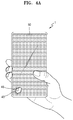
- FIGS. 4A through 4C illustrates various examples of gripping the display apparatus 1 . with one hand by using the through hole 40 formed in the display apparatus 1 .
- the speaker port 50 is understood to be a speaker of a mobile telephone, i.e. the part of the mobile telephone that would be held to a user's ear while the opposite side would be held to a user's mouth.
- FIG. 4A illustrates an example of holding the display apparatus 1 by inserting the little finger of the right hand into the through hole 40 located at a left lower end of the display apparatus 1 while surrounding the display apparatus 1 with the other fingers.
- FIG. 4B illustrates an example of holding the display apparatus 1 by inserting the index finger of the right hand into the through hole 40 located at a left upper end of the display apparatus 1 and surrounding the display apparatus 1 with the other fingers.
- FIG. 4C illustrates an example of holding the display apparatus 1 by inserting the index finger of the right hand through the through hole 40 located at an upper end center of the display apparatus 1 .
- the display apparatus 1 may be held by hanging the display apparatus 1 on a hook 70 installed on a wall W or automobile panel, through the through hole 40 .
- FIGS. 6A through 6E illustrate examples of the through hole 40 at various locations according to an exemplary embodiment of the present invention.
- FIG. 6A illustrates an example in which the through hole 40 is located at a right lower end of the display apparatus 1 .
- FIG. 6B illustrates an example in which the through hole 40 is in an upper end center of the display apparatus 1 .
- FIG. 6C illustrates an example in which the through hole 40 is between a left upper end and a left lower end of the display apparatus 1 .
- FIG. 6D illustrates an example in which the through hole 40 is almost in a lower end center of the display apparatus 1 .
- FIG. 6E illustrates a through hole 40 in a center of a display apparatus 2 having a circular shape.
- a location of the through hole 40 is not limited to the embodiments of FIGS. 6A through 6E , and may be modified in various manners according to design purposes.
- FIGS. 7A through 7D illustrate various forms of the through hole 40 .
- FIG. 7A illustrates the through hole 40 having an oval shape.
- FIG. 7B illustrates the through hole 40 having a square shape with round corners.
- FIG. 7C illustrates the through hole 40 having a rectangular shape with round corners.
- FIG. 7D illustrates the through hole 40 having a shape that is close to a hexagon.
- the shape of the through hole 40 according to an exemplary embodiment of the present invention is not limited to the manner shown in FIGS. 7A through 7D , and may be modified in various manners according to design purposes.
- FIGS. 8A and 8B illustrate examples of various numbers of through holes 40 .
- FIG. 8A illustrates through holes 40 located at a left upper end and a left lower end of the display apparatus 1 .
- FIG. 8B illustrates two through holes 40 along a diagonal line at a left lower end and a right upper end of the display apparatus 1 .
- the number and location of the through holes 40 according to an exemplary embodiment of the present invention are not limited to the manners shown in FIGS. 8A and 8B , and may be modified in various manners according to design purposes.
- FIGS. 9A and 9B illustrate examples of the through hole 40 at various locations according to an exemplary embodiment of the present invention.
- FIG. 9A illustrates that the through hole 40 is formed over the active area AA and the non-active area NA of the display apparatus 1 .
- FIG. 9B illustrates that the through hole 40 is formed only in the non-active area NA of the display apparatus 1 .
- the through hole 40 may be formed in the active area AA where an image is displayed.
- an effective display area of the active area AA displaying an image may be extended by forming a signal input element such as a button, a wheel, or a switch in an outline area 45 of the through hole 40 .
- the signal input element may be formed as a contact type or a non-contact type.
- a signal sensing element such as an optical sensor, a tactile sensor, a pressure sensor, or a fingerprint recognition sensor may be formed in the outline area 45 of the through hole 40 .
- the tactile sensor may include a touch sensor of a capacitive type, an infrared ray type, a resistive type, or a photoelectric type.
- the signal sensing element may be formed as a contact type or a non-contact type.
- the through hole 40 may also be applied. to a display apparatus 3 illustrated in FIG. 10 according to an exemplary embodiment of the present invention.
- An active area AA of the display apparatus 3 displaying an image may include a first active area AA 1 formed over a front surface of the display apparatus 3 and a second active area AA 2 formed over a side surface of the display apparatus 3 .
- FIG. 10 illustrates that the second active area AA 2 is formed only over one side surface of the display apparatus 3
- the second active area AA 2 may also be formed over the other side surfaces of the display apparatus 3 .
- a location of the through hole 40 according to an exemplary embodiment of the present invention is not limited to the manners illustrated in FIGS. 9A and 9B , and may be modified in various manners according to design purposes.
- the cover layer 10 may be formed of a material having a high transmittivity so that an image emitted from the display panel 20 may be transmitted through the cover layer 10 .
- the cover layer 10 may be formed of a material having an appropriate rigidity so as to protect the display panel 20 from an external impact.
- the active area When an active area is formed not only over a front surface of the cover layer 10 and the display panel 20 but also over a side surface of the display apparatus 3 as in the display apparatus 3 illustrated in FIG. 10 , the active area may be extended up to the side surface of the display apparatus 3 .
- the housing 30 in which the display panel 20 is mounted, may be a single-body element, and a portion of a side surface 32 or a rear portion 33 of the housing 30 may he combined to another body to form a multi-bodied structure.
- a thickness of the side surface 32 of the housing 30 is illustrated in FIG. 2 as being identical to a sum of a thickness of the display panel 20 and a thickness of the cover layer 10 , the invention is not limited to this arrangement.
- a height of the side surface 32 of the housing 30 may be modified in various manners according to design purposes.
- the housing 30 may be formed of a material having an appropriate rigidity to protect the display panel 20 from an external impact.
- the housing 30 may be formed of various materials such as plastic, metal, glass, or ceramic.
- the substrate 21 may include various materials.
- the substrate 21 may be formed of glass, metal, or an organic material.
- the substrate 21 may be formed of a flexible material so that the substrate 21 may be easily bent, curved, folded or rolled.
- the substrate 21 may be formed of ultrathin glass, metal or plastic.
- the substrate 21 may be formed of polyimide (PI), but this is exemplary, and the substrate 21 may be formed of various materials.
- a barrier layer (not shown) may be further included between the substrate 21 and the display layer 22 .
- the barrier layer prevents exterior moisture or oxygen from penetrating into the substrate 21 through the display layer 22 .
- the barrier layer may be formed of an inorganic material such as a metal oxide, a silicon nitride or a silicon oxide.
- the barrier layer may include an inorganic layer such as AlO 3 , SiO 2 , or SiN x and may be formed as a single layer or as a multiple layer.
- the display layer 22 may include an inorganic light-emitting diode, an organic light-emitting diode, an electronic ink element, a liquid crystal display device element or a pixel P formed from other appropriate display pixel structures.
- the display layer 22 including an organic light-emitting diode may further include a first electrode 221 , a second electrode 222 , and an intermediate layer 223 .
- the first electrode 221 may be formed of various conductive materials.
- the first electrode 221 may be patterned.
- the first electrode 221 may include at least one material selected from a group consisting of an indium tin oxide (ITO), indium zinc oxide (IZO), a zinc oxide (ZnO), an indium oxide (In 2 O 3 ), an indium gallium oxide (IGO), and an aluminum zinc oxide (AZO).
- the first electrode 221 may further include silver (Ag) or an Ag alloy.
- the intermediate layer 223 may include an organic emissive layer (not shown), and the organic emissive layer may be a small-molecule organic material or a polymer organic material,
- the intermediate layer 223 may include, in addition to the organic emissive layer, a hole injection layer, a hole transport layer, an electron transport layer, and/or an electron injection layer.
- the second electrode 222 may be formed of various conductive materials.
- the second electrode 222 may include a lithium (Li), calcium (Ca), lithium fluoride (LiF), aluminum (Al), magnesium (Mg) or silver (Ag), and may include a single layer or a multi-layer structure by using at least one of the above materials, and may include an alloy material including at least two of the above materials.
- the second electrode 222 may have a thickness providing an appropriate transmittivity so that an image may pass through the cover layer 10 .
- the encapsulation layer 23 may be disposed over the second electrode.
- the encapsulation layer 23 may include a plurality of inorganic layers or may include a combination including at least one organic layer and at least one inorganic layer.
- the organic layer may be formed of a polymer, and may be a single layer or a multi-layer structure including polyethylene terephthalate, polyimide, polycarbonate, epoxy, polyethylene, and/or polyacrylate.
- the organic layer may be formed of polyacrylate, and may include, for example, a monomer composition that includes a diacrylate-based monomer and a triacrylate-based monomer and is polymerized.
- the monomer composition may further include a monoacrylate-based monomer.
- the monomer composition may include a photo-initiator such as a trimethylbenzoyl phenylphosphine oxide (TPO), but the invention is not limited thereto.
- TPO trimethylbenzoyl phenylphosphine oxide
- the inorganic layer may be a single layer or a multi-layer structure including a metal oxide or a metal nitride.
- the inorganic layer may include SiNx, Al 2 O 3 , SiO 2 , and/or TiO 2 .
- the encapsulation layer 23 may include at least one sandwich structure in which at least one organic layer is disposed between at least two inorganic layers. Also, the encapsulation layer 23 may include at least one sandwich structure in which at least one inorganic layer is disposed between at least two organic layers.
- a metal halide layer including LiF may be additionally included between the display layer 22 and the inorganic layer.
- the metal halide layer may prevent damage to the display layer 22 when the inorganic layer is formed using a sputtering method or a plasma deposition method.
- the encapsulation layer 23 might not only encapsulate an upper surface of the display layer 22 but may also surround a side surface of the display layer 22 adjacent to an inner circumferential surface of the through hole 40 in an area where the through hole 40 is formed.
- An outermost portion of the encapsulation layer 23 that surrounds the side surface of the display layer 22 may include an inorganic layer.
- the encapsulation layer 23 having a structure as described above may prevent penetration of impurities such as oxygen or moisture from the outside environment of the display apparatus 1 , into the display panel 20 .
- FIGS. 11A through 11E illustrate examples in which an element P is formed in an outline area 45 of the through hole 40 .
- the outside area is an area that immediately surrounds the through hole 40 .
- FIG. 11A illustrates that elements 60 are formed in the outline area 45 of the through hole 40 .
- the element 60 may be a signal sensing element such as an optical sensor, an acoustic sensor, a tactile sensor, a pressure sensor, or a fingerprint recognition sensor or a signal input element such as a button, a wheel, or a switch.
- a signal sensing element such as an optical sensor, an acoustic sensor, a tactile sensor, a pressure sensor, or a fingerprint recognition sensor
- a signal input element such as a button, a wheel, or a switch.
- FIG. 11B illustrates an example in which elements 60 are formed over the outline area 45
- FIG. 11C illustrates an example in which elements 60 are formed below the outline area 45
- FIG. 11D illustrates an example in which elements 60 are formed on an inner circumferential surface of the through hole 40 in the outline area 45 .
- elements P may be integrally formed with the cover layer 10 of the display apparatus 1 . While not illustrated in FIG. 11B , elements P may be disposed between the encapsulation layer 23 and the cover layer 10 . Also, the elements P may be formed over the cover layer 10 .
- FIG. 11E illustrates an example in which elements P are capacitive elements including a first electrode 61 and a second electrode 62 .
- the capacitive element may be driven using various methods such as an electrostatic capacity method or a resistance capacity method.
- the first electrode 61 and the second electrode 62 may be formed in the cover layer 10 of the display apparatus 1 .
- a third electrode (not shown) may be further formed.
- first electrode 61 and the second electrode 62 may be formed between the encapsulation layer 23 and the cover layer 10 .
- design whereby the active area AA displaying an image of the display apparatus 1 may be extended by forming the elements P according to the above-described various embodiments in the outline area 45 around the through hole 40 may be possible, and various applications using the elements P may be used.
- FIG. 12A is a cross-sectional view illustrating a wheel 46 formed in an outline around a through hole 40 according to an exemplary embodiment of the present invention
- FIG. 12B is a cross-sectional view of a portion of the display apparatus 1 including the through hole 40 described above.
- a predetermined signal may be input to the display apparatus 1 by rotating the wheel 46 .
- the wheel 46 which that is rotatable by a physical rotational force, may be formed in the outline area 45 of the through hole 40 .
- the wheel 46 may further include a sensing element that senses a touch.
- FIG. 13A is a cross-sectional view illustrating a button 47 formed in an outline around a through hole 40 according to an exemplary embodiment of the present invention
- FIG. 13B is a cross-sectional view of a portion of the display apparatus 1 including the through hole 40 described above.
- a predetermined signal may be input to the display apparatus 1 by applying pressure to the button 47 .
- the button 47 that is moved upwards or downwards by receiving physical pressure may be formed in the outline area 45 of the through hole 40 .
- a sensing element sensing information via a touch may be further added to the button 47 .
- FIGS. 14A and 14B illustrate the through hole 40 of the display apparatus 1 used as a connection terminal of a charger 80 , according to an exemplary embodiment of the present invention.
- portable electronic devices such as mobile phones my use wireless charging methods to charge power to the device using an inductive coil portion installed therein.
- the inductive coil portion may have a rectangular parallelepiped shape and a predetermined thickness and may be formed inside a display apparatus. In this case, a total thickness of the display apparatus is increased due to the inductive coil portion, and thus a slim design may be difficult to obtain in a device utilizing inductive charging.
- the display apparatus may be charged using a wireless charging method by installing a first inductive coil portion 82 on a protrusion 83 of the charger 80 and forming a wireless charging connection terminal such as a second inductive coil portion 81 in the outline area 45 of the through hole 40 , and inserting the protrusion 83 into the through hole 40 .
- the display apparatus 1 By disposing the second inductive coil portion 81 in the through hole 40 , the display apparatus 1 having a slim design may be provided.
- the charging method performed by inserting the protrusion 83 of the charger 80 into the through hole 40 may interest users and may alleviate a problem that is common to inductive charging where charging can be interrupted if the wireless device is displaced from its proper positon.
- Some approaches utilize magnets to help keep the device in place while being charged, but this approach may be difficult to produce and may offer only limited success.
- inserting the protrusion into the through hole 40 may ensure the device remains in the optimal positon for wireless charging and lessens the risk that a user may return to a device that has not been properly charged after leaving the device on a wireless charging station for an extended period of time.
- the outline area 45 of the display apparatus 1 may include an insulation member,
- the insulation member may cover the second inductive coil portion 81 to prevent a short circuit between the first inductive coil portion 82 and the second inductive coil portion 81 .
- a manufacturing process of an organic light-emitting display apparatus may be simplified, and misalignment of patterns may be prevented.
- an efficiency of the organic light-emitting display apparatus may be increased, and a lifetime of the organic light-emitting display apparatus may be extended.
Landscapes
- Engineering & Computer Science (AREA)
- Theoretical Computer Science (AREA)
- Physics & Mathematics (AREA)
- General Physics & Mathematics (AREA)
- Human Computer Interaction (AREA)
- Signal Processing (AREA)
- Computer Hardware Design (AREA)
- General Engineering & Computer Science (AREA)
- Multimedia (AREA)
- Microelectronics & Electronic Packaging (AREA)
- Power Engineering (AREA)
- Computer Networks & Wireless Communication (AREA)
- Devices For Indicating Variable Information By Combining Individual Elements (AREA)
- Electroluminescent Light Sources (AREA)
Abstract
Description
Claims (20)
Applications Claiming Priority (2)
| Application Number | Priority Date | Filing Date | Title |
|---|---|---|---|
| KR10-2015-0163349 | 2015-11-20 | ||
| KR1020150163349A KR102388722B1 (en) | 2015-11-20 | 2015-11-20 | Display apparatus and organic light-emitting display apparatus |
Publications (2)
| Publication Number | Publication Date |
|---|---|
| US20170150618A1 US20170150618A1 (en) | 2017-05-25 |
| US10609826B2 true US10609826B2 (en) | 2020-03-31 |
Family
ID=58721571
Family Applications (1)
| Application Number | Title | Priority Date | Filing Date |
|---|---|---|---|
| US15/336,944 Active 2037-07-18 US10609826B2 (en) | 2015-11-20 | 2016-10-28 | Display apparatus having a full-thickness through hole |
Country Status (3)
| Country | Link |
|---|---|
| US (1) | US10609826B2 (en) |
| KR (1) | KR102388722B1 (en) |
| CN (1) | CN106782107B (en) |
Cited By (7)
| Publication number | Priority date | Publication date | Assignee | Title |
|---|---|---|---|---|
| USD933654S1 (en) * | 2017-10-13 | 2021-10-19 | Samsung Display Co., Ltd. | Display device |
| US11374199B2 (en) * | 2019-09-30 | 2022-06-28 | Wuhan China Star Optoelectronics Semiconductor Display Technology Co., Ltd. | Display panel and display device having through hole surrounding barrier area |
| USD971211S1 (en) * | 2018-07-23 | 2022-11-29 | Samsung Display Co., Ltd. | Display module |
| US11594818B2 (en) | 2020-03-06 | 2023-02-28 | Samsung Display Co., Ltd. | Electronic apparatus |
| US11818940B2 (en) | 2019-07-05 | 2023-11-14 | Samsung Display Co., Ltd. | Electronic apparatus including an electronic module and method of manufacturing the same |
| US12075645B2 (en) | 2018-06-28 | 2024-08-27 | Samsung Display Co., Ltd. | Display device |
| US12356829B2 (en) | 2018-10-12 | 2025-07-08 | Samsung Display Co., Ltd. | Electronic apparatus |
Families Citing this family (33)
| Publication number | Priority date | Publication date | Assignee | Title |
|---|---|---|---|---|
| KR102605208B1 (en) | 2016-06-28 | 2023-11-24 | 삼성디스플레이 주식회사 | Organic light emitting display device and method of manufacturing an organic light emitting display device |
| KR102103962B1 (en) | 2016-09-02 | 2020-06-01 | 삼성디스플레이 주식회사 | Display device and manufacturing method thereof |
| KR102083646B1 (en) | 2017-08-11 | 2020-03-03 | 삼성디스플레이 주식회사 | Display panel and electronic device having the same |
| KR102083315B1 (en) | 2017-09-11 | 2020-03-03 | 삼성디스플레이 주식회사 | Organic light-emitting display device and method of manufacturing the same |
| KR102530926B1 (en) * | 2017-12-27 | 2023-05-09 | 엘지디스플레이 주식회사 | Fingerprint sensing display apparatus |
| CN107658332A (en) * | 2017-10-25 | 2018-02-02 | 京东方科技集团股份有限公司 | A kind of display panel, display device and preparation method |
| US11482694B2 (en) | 2017-10-25 | 2022-10-25 | Boe Technology Group Co., Ltd. | Display panel, method for fabricating the same, and display device |
| CN107786696B (en) * | 2017-12-13 | 2024-06-18 | 京东方科技集团股份有限公司 | Display screen and mobile terminal |
| KR20190108212A (en) | 2018-03-13 | 2019-09-24 | 삼성디스플레이 주식회사 | Display panel and method of manufacturing display apparatus including the same |
| USD914024S1 (en) * | 2018-03-26 | 2021-03-23 | Huawei Technologies Co., Ltd. | Display screen for telephone |
| US11201307B2 (en) * | 2018-04-17 | 2021-12-14 | Samsung Display Co., Ltd. | Display panel and electronic apparatus including the same |
| EP3780110B1 (en) * | 2018-05-08 | 2024-05-01 | Huawei Technologies Co., Ltd. | Mobile terminal having flexible display panel |
| US10541380B1 (en) | 2018-08-30 | 2020-01-21 | Samsung Display Co., Ltd. | Display device with substrate comprising an opening and adjacent grooves |
| KR102608021B1 (en) * | 2018-09-03 | 2023-12-01 | 삼성디스플레이 주식회사 | Electronic apparatus and method of manufacturing the same |
| KR102661469B1 (en) | 2018-09-11 | 2024-04-29 | 삼성디스플레이 주식회사 | Display panel |
| KR102697457B1 (en) | 2018-10-11 | 2024-08-22 | 삼성디스플레이 주식회사 | Display panel |
| KR102737768B1 (en) * | 2018-11-02 | 2024-12-04 | 삼성디스플레이 주식회사 | Display panel and electronic device including the same |
| KR102627937B1 (en) * | 2018-11-27 | 2024-01-23 | 삼성디스플레이 주식회사 | Display panel |
| KR102643634B1 (en) | 2018-12-04 | 2024-03-06 | 삼성디스플레이 주식회사 | Display panel |
| KR102756394B1 (en) * | 2019-01-10 | 2025-01-21 | 삼성디스플레이 주식회사 | Display device |
| KR102778473B1 (en) | 2019-01-21 | 2025-03-12 | 삼성디스플레이 주식회사 | Display device |
| US20200280018A1 (en) * | 2019-02-28 | 2020-09-03 | Oledworks Gmbh | Oled with pass-through hole |
| KR102806400B1 (en) | 2019-03-08 | 2025-05-13 | 삼성디스플레이 주식회사 | Display panel |
| CN109801956A (en) * | 2019-03-13 | 2019-05-24 | 京东方科技集团股份有限公司 | Display device, display panel and its manufacturing method |
| KR102704013B1 (en) * | 2019-04-11 | 2024-09-10 | 삼성디스플레이 주식회사 | Display module, manufacturing method for display module, and laser machining method |
| KR102896748B1 (en) | 2019-06-19 | 2025-12-05 | 삼성디스플레이 주식회사 | Display panel |
| KR20210002232A (en) | 2019-06-28 | 2021-01-07 | 삼성디스플레이 주식회사 | Display panel and display device |
| KR102720609B1 (en) * | 2019-07-19 | 2024-10-24 | 삼성디스플레이 주식회사 | Flexible display device |
| KR102914174B1 (en) | 2019-10-30 | 2026-01-16 | 삼성디스플레이 주식회사 | Display apparatus and manufacturing the same |
| KR20210052749A (en) | 2019-10-31 | 2021-05-11 | 삼성디스플레이 주식회사 | Display apparatus and electronic apparatus having the same |
| KR102852522B1 (en) | 2020-11-25 | 2025-09-02 | 삼성디스플레이 주식회사 | Display device and method of manufacturing the same |
| WO2023119429A1 (en) * | 2021-12-21 | 2023-06-29 | 日本電信電話株式会社 | Antenna device, wireless electric power transfer device, and wireless electric power transfer system |
| CN115691325B (en) * | 2022-09-06 | 2025-07-15 | 武汉天马微电子有限公司 | Display panel and display device |
Citations (16)
| Publication number | Priority date | Publication date | Assignee | Title |
|---|---|---|---|---|
| US20040021410A1 (en) | 2002-08-01 | 2004-02-05 | Eastman Kodak Company | Method and apparatus for making a shadow mask array |
| US20050157457A1 (en) | 2004-01-19 | 2005-07-21 | Kwey-Hyun Kim | Display apparatus and method of making the same |
| US20080123178A1 (en) * | 2006-11-28 | 2008-05-29 | Seiko Epson Corporation | Electro-optical device, method of manufacturing electro-optical device and electronic apparatus |
| US20120044181A1 (en) | 2010-08-23 | 2012-02-23 | Samsung Electronics Co. Ltd. | On-cell tsp active matrix organic light emitting diode structure |
| WO2012148052A1 (en) | 2011-04-27 | 2012-11-01 | Choi Dong-Il | Device for mounting a portable phone |
| CN102915084A (en) | 2012-10-09 | 2013-02-06 | 李铁 | Tablet computer convenient to hold |
| US20130076649A1 (en) * | 2011-09-27 | 2013-03-28 | Scott A. Myers | Electronic Devices With Sidewall Displays |
| CN103235637A (en) | 2013-04-15 | 2013-08-07 | 李铁 | Intelligent terminal convenient for single-hand holding |
| KR20140022584A (en) | 2012-08-14 | 2014-02-25 | 서재홍 | Smart infra-red input device |
| US20140061610A1 (en) * | 2012-08-31 | 2014-03-06 | Hyo-Young MUN | Organic light emitting device and manufacturing method thereof |
| KR20140068048A (en) | 2011-09-07 | 2014-06-05 | 알레그로 마이크로시스템스, 엘엘씨 | Magnetic field sensing element combining a circular vertical hall magnetic field sensing element with a planar hall element |
| CN103997085A (en) | 2014-05-06 | 2014-08-20 | 昆山佑翔电子科技有限公司 | Dustproof heat-dissipating wireless charger |
| CN104069977A (en) | 2013-03-28 | 2014-10-01 | 三星显示有限公司 | Deposition apparatus, method for forming thin film using the same, organic light emitting display apparatus and method for manufacturing the same |
| US20150144934A1 (en) * | 2011-10-14 | 2015-05-28 | Apple Inc. | Electronic Devices Having Displays With Openings |
| KR20150077159A (en) | 2013-12-27 | 2015-07-07 | 엘지디스플레이 주식회사 | Touch Display Device Having Function of Mouse And Method Of Driving The Same |
| US20170031323A1 (en) * | 2015-07-29 | 2017-02-02 | Lg Display Co., Ltd. | Organic light emitting display device |
Family Cites Families (3)
| Publication number | Priority date | Publication date | Assignee | Title |
|---|---|---|---|---|
| JP5151739B2 (en) * | 2008-07-02 | 2013-02-27 | カシオ計算機株式会社 | Light emitting panel for pointer board and method for manufacturing light emitting panel for pointer board |
| KR101424519B1 (en) * | 2012-11-14 | 2014-08-01 | 윤성진 | Mobile terminal |
| KR102000716B1 (en) * | 2014-08-26 | 2019-07-17 | 삼성디스플레이 주식회사 | Organic light emitting display apparatus and the method for manufacturing the same |
-
2015
- 2015-11-20 KR KR1020150163349A patent/KR102388722B1/en active Active
-
2016
- 2016-10-28 US US15/336,944 patent/US10609826B2/en active Active
- 2016-11-21 CN CN201611047913.4A patent/CN106782107B/en active Active
Patent Citations (18)
| Publication number | Priority date | Publication date | Assignee | Title |
|---|---|---|---|---|
| US20040021410A1 (en) | 2002-08-01 | 2004-02-05 | Eastman Kodak Company | Method and apparatus for making a shadow mask array |
| US20050157457A1 (en) | 2004-01-19 | 2005-07-21 | Kwey-Hyun Kim | Display apparatus and method of making the same |
| CN1645191A (en) | 2004-01-19 | 2005-07-27 | 三星电子株式会社 | Display apparatus and method of making the same |
| US20080123178A1 (en) * | 2006-11-28 | 2008-05-29 | Seiko Epson Corporation | Electro-optical device, method of manufacturing electro-optical device and electronic apparatus |
| US20120044181A1 (en) | 2010-08-23 | 2012-02-23 | Samsung Electronics Co. Ltd. | On-cell tsp active matrix organic light emitting diode structure |
| WO2012148052A1 (en) | 2011-04-27 | 2012-11-01 | Choi Dong-Il | Device for mounting a portable phone |
| KR20140068048A (en) | 2011-09-07 | 2014-06-05 | 알레그로 마이크로시스템스, 엘엘씨 | Magnetic field sensing element combining a circular vertical hall magnetic field sensing element with a planar hall element |
| US20130076649A1 (en) * | 2011-09-27 | 2013-03-28 | Scott A. Myers | Electronic Devices With Sidewall Displays |
| US20150144934A1 (en) * | 2011-10-14 | 2015-05-28 | Apple Inc. | Electronic Devices Having Displays With Openings |
| KR20140022584A (en) | 2012-08-14 | 2014-02-25 | 서재홍 | Smart infra-red input device |
| US20140061610A1 (en) * | 2012-08-31 | 2014-03-06 | Hyo-Young MUN | Organic light emitting device and manufacturing method thereof |
| CN102915084A (en) | 2012-10-09 | 2013-02-06 | 李铁 | Tablet computer convenient to hold |
| US9306192B2 (en) | 2013-03-28 | 2016-04-05 | Samsung Display Co., Ltd. | Deposition apparatus, method for forming thin film using the same, organic light emitting display apparatus and method for manufacturing the same |
| CN104069977A (en) | 2013-03-28 | 2014-10-01 | 三星显示有限公司 | Deposition apparatus, method for forming thin film using the same, organic light emitting display apparatus and method for manufacturing the same |
| CN103235637A (en) | 2013-04-15 | 2013-08-07 | 李铁 | Intelligent terminal convenient for single-hand holding |
| KR20150077159A (en) | 2013-12-27 | 2015-07-07 | 엘지디스플레이 주식회사 | Touch Display Device Having Function of Mouse And Method Of Driving The Same |
| CN103997085A (en) | 2014-05-06 | 2014-08-20 | 昆山佑翔电子科技有限公司 | Dustproof heat-dissipating wireless charger |
| US20170031323A1 (en) * | 2015-07-29 | 2017-02-02 | Lg Display Co., Ltd. | Organic light emitting display device |
Non-Patent Citations (1)
| Title |
|---|
| Chinese Office Action dated Dec. 27, 2019 for Chinese Application Serial No. 201611047913.4. |
Cited By (8)
| Publication number | Priority date | Publication date | Assignee | Title |
|---|---|---|---|---|
| USD933654S1 (en) * | 2017-10-13 | 2021-10-19 | Samsung Display Co., Ltd. | Display device |
| USD1098107S1 (en) | 2017-10-13 | 2025-10-14 | Samsung Display Co., Ltd. | Display device |
| US12075645B2 (en) | 2018-06-28 | 2024-08-27 | Samsung Display Co., Ltd. | Display device |
| USD971211S1 (en) * | 2018-07-23 | 2022-11-29 | Samsung Display Co., Ltd. | Display module |
| US12356829B2 (en) | 2018-10-12 | 2025-07-08 | Samsung Display Co., Ltd. | Electronic apparatus |
| US11818940B2 (en) | 2019-07-05 | 2023-11-14 | Samsung Display Co., Ltd. | Electronic apparatus including an electronic module and method of manufacturing the same |
| US11374199B2 (en) * | 2019-09-30 | 2022-06-28 | Wuhan China Star Optoelectronics Semiconductor Display Technology Co., Ltd. | Display panel and display device having through hole surrounding barrier area |
| US11594818B2 (en) | 2020-03-06 | 2023-02-28 | Samsung Display Co., Ltd. | Electronic apparatus |
Also Published As
| Publication number | Publication date |
|---|---|
| US20170150618A1 (en) | 2017-05-25 |
| KR20170059527A (en) | 2017-05-31 |
| CN106782107B (en) | 2020-09-29 |
| CN106782107A (en) | 2017-05-31 |
| KR102388722B1 (en) | 2022-04-21 |
Similar Documents
| Publication | Publication Date | Title |
|---|---|---|
| US10609826B2 (en) | Display apparatus having a full-thickness through hole | |
| US10957874B2 (en) | Display panel and electronic device including the same | |
| JP2024149678A (en) | Touch Panel | |
| KR102699192B1 (en) | Display device | |
| JP6678406B2 (en) | Peeling method | |
| CN210379052U (en) | Array substrate and display device | |
| KR102560702B1 (en) | Display device | |
| US20150357387A1 (en) | Flexible display device | |
| CN106814912A (en) | A kind of pressure touch sensor, display device and its driving method | |
| KR102712985B1 (en) | Semiconductor device | |
| US9335855B2 (en) | Top-emitting OLED display having transparent touch panel | |
| KR20170006261A (en) | Touch sensor and touch panel | |
| US11024653B2 (en) | Display device | |
| US12326754B2 (en) | Digitizer and display apparatus including the same | |
| JP2016027559A (en) | LIGHT EMITTING DEVICE, MODULE, AND ELECTRONIC DEVICE | |
| KR20160000980A (en) | Organic light emitting display device | |
| CN217280778U (en) | display device | |
| TW201032111A (en) | System for display images | |
| CN107168570A (en) | Array base palte, touch-control display module, electronic equipment and fingerprint identification method | |
| KR20210063529A (en) | Display device and method of manufacturing the same | |
| US20250176409A1 (en) | Electronic device | |
| KR101895594B1 (en) | Object displaying method for distinguishing applacations having a touch pressure function and a mobile terminal using the same | |
| CN114583081B (en) | Display panel and preparation method thereof | |
| US20260026248A1 (en) | Display device and electronic device including the same | |
| CN109558023A (en) | Touch display screen and terminal device |
Legal Events
| Date | Code | Title | Description |
|---|---|---|---|
| AS | Assignment |
Owner name: SAMSUNG DISPLAY CO., LTD., KOREA, REPUBLIC OF Free format text: ASSIGNMENT OF ASSIGNORS INTEREST;ASSIGNORS:CHOI, JONGHYUN;KANG, KINYENG;KIM, SUNKWANG;REEL/FRAME:040157/0901 Effective date: 20161024 |
|
| STPP | Information on status: patent application and granting procedure in general |
Free format text: NON FINAL ACTION MAILED |
|
| STPP | Information on status: patent application and granting procedure in general |
Free format text: RESPONSE TO NON-FINAL OFFICE ACTION ENTERED AND FORWARDED TO EXAMINER |
|
| STPP | Information on status: patent application and granting procedure in general |
Free format text: FINAL REJECTION MAILED |
|
| STPP | Information on status: patent application and granting procedure in general |
Free format text: ADVISORY ACTION MAILED |
|
| STPP | Information on status: patent application and granting procedure in general |
Free format text: DOCKETED NEW CASE - READY FOR EXAMINATION |
|
| STPP | Information on status: patent application and granting procedure in general |
Free format text: NOTICE OF ALLOWANCE MAILED -- APPLICATION RECEIVED IN OFFICE OF PUBLICATIONS |
|
| STPP | Information on status: patent application and granting procedure in general |
Free format text: AWAITING TC RESP, ISSUE FEE PAYMENT VERIFIED |
|
| STPP | Information on status: patent application and granting procedure in general |
Free format text: AWAITING TC RESP, ISSUE FEE PAYMENT VERIFIED |
|
| STCF | Information on status: patent grant |
Free format text: PATENTED CASE |
|
| MAFP | Maintenance fee payment |
Free format text: PAYMENT OF MAINTENANCE FEE, 4TH YEAR, LARGE ENTITY (ORIGINAL EVENT CODE: M1551); ENTITY STATUS OF PATENT OWNER: LARGE ENTITY Year of fee payment: 4 |