US10609812B2 - Printed circuit board, optical module, and optical transmission equipment - Google Patents
Printed circuit board, optical module, and optical transmission equipment Download PDFInfo
- Publication number
- US10609812B2 US10609812B2 US15/835,532 US201715835532A US10609812B2 US 10609812 B2 US10609812 B2 US 10609812B2 US 201715835532 A US201715835532 A US 201715835532A US 10609812 B2 US10609812 B2 US 10609812B2
- Authority
- US
- United States
- Prior art keywords
- pair
- orientation
- resonator
- circuit board
- printed circuit
- Prior art date
- Legal status (The legal status is an assumption and is not a legal conclusion. Google has not performed a legal analysis and makes no representation as to the accuracy of the status listed.)
- Active, expires
Links
Images


Classifications
-
- H—ELECTRICITY
- H05—ELECTRIC TECHNIQUES NOT OTHERWISE PROVIDED FOR
- H05K—PRINTED CIRCUITS; CASINGS OR CONSTRUCTIONAL DETAILS OF ELECTRIC APPARATUS; MANUFACTURE OF ASSEMBLAGES OF ELECTRICAL COMPONENTS
- H05K1/00—Printed circuits
- H05K1/02—Details
- H05K1/0213—Electrical arrangements not otherwise provided for
- H05K1/0216—Reduction of cross-talk, noise or electromagnetic interference
- H05K1/0228—Compensation of cross-talk by a mutually correlated lay-out of printed circuit traces, e.g. for compensation of cross-talk in mounted connectors
-
- H—ELECTRICITY
- H01—ELECTRIC ELEMENTS
- H01P—WAVEGUIDES; RESONATORS, LINES, OR OTHER DEVICES OF THE WAVEGUIDE TYPE
- H01P1/00—Auxiliary devices
- H01P1/20—Frequency-selective devices, e.g. filters
-
- G—PHYSICS
- G02—OPTICS
- G02B—OPTICAL ELEMENTS, SYSTEMS OR APPARATUS
- G02B6/00—Light guides; Structural details of arrangements comprising light guides and other optical elements, e.g. couplings
- G02B6/24—Coupling light guides
- G02B6/42—Coupling light guides with opto-electronic elements
- G02B6/4201—Packages, e.g. shape, construction, internal or external details
- G02B6/4274—Electrical aspects
- G02B6/4279—Radio frequency signal propagation aspects of the electrical connection, high frequency adaptations
-
- G—PHYSICS
- G02—OPTICS
- G02B—OPTICAL ELEMENTS, SYSTEMS OR APPARATUS
- G02B6/00—Light guides; Structural details of arrangements comprising light guides and other optical elements, e.g. couplings
- G02B6/24—Coupling light guides
- G02B6/42—Coupling light guides with opto-electronic elements
- G02B6/4201—Packages, e.g. shape, construction, internal or external details
- G02B6/4274—Electrical aspects
- G02B6/428—Electrical aspects containing printed circuit boards [PCB]
- G02B6/4281—Electrical aspects containing printed circuit boards [PCB] the printed circuit boards being flexible
-
- G—PHYSICS
- G02—OPTICS
- G02B—OPTICAL ELEMENTS, SYSTEMS OR APPARATUS
- G02B6/00—Light guides; Structural details of arrangements comprising light guides and other optical elements, e.g. couplings
- G02B6/24—Coupling light guides
- G02B6/42—Coupling light guides with opto-electronic elements
- G02B6/4201—Packages, e.g. shape, construction, internal or external details
- G02B6/4274—Electrical aspects
- G02B6/4284—Electrical aspects of optical modules with disconnectable electrical connectors
-
- H—ELECTRICITY
- H01—ELECTRIC ELEMENTS
- H01P—WAVEGUIDES; RESONATORS, LINES, OR OTHER DEVICES OF THE WAVEGUIDE TYPE
- H01P1/00—Auxiliary devices
- H01P1/20—Frequency-selective devices, e.g. filters
- H01P1/201—Filters for transverse electromagnetic waves
- H01P1/203—Strip line filters
- H01P1/20327—Electromagnetic interstage coupling
- H01P1/20354—Non-comb or non-interdigital filters
- H01P1/20381—Special shape resonators
-
- H—ELECTRICITY
- H01—ELECTRIC ELEMENTS
- H01P—WAVEGUIDES; RESONATORS, LINES, OR OTHER DEVICES OF THE WAVEGUIDE TYPE
- H01P3/00—Waveguides; Transmission lines of the waveguide type
- H01P3/02—Waveguides; Transmission lines of the waveguide type with two longitudinal conductors
- H01P3/026—Coplanar striplines [CPS]
-
- H—ELECTRICITY
- H01—ELECTRIC ELEMENTS
- H01P—WAVEGUIDES; RESONATORS, LINES, OR OTHER DEVICES OF THE WAVEGUIDE TYPE
- H01P3/00—Waveguides; Transmission lines of the waveguide type
- H01P3/02—Waveguides; Transmission lines of the waveguide type with two longitudinal conductors
- H01P3/08—Microstrips; Strip lines
- H01P3/081—Microstriplines
-
- H—ELECTRICITY
- H01—ELECTRIC ELEMENTS
- H01P—WAVEGUIDES; RESONATORS, LINES, OR OTHER DEVICES OF THE WAVEGUIDE TYPE
- H01P7/00—Resonators of the waveguide type
- H01P7/08—Strip line resonators
- H01P7/086—Coplanar waveguide resonators
-
- H—ELECTRICITY
- H04—ELECTRIC COMMUNICATION TECHNIQUE
- H04B—TRANSMISSION
- H04B10/00—Transmission systems employing electromagnetic waves other than radio-waves, e.g. infrared, visible or ultraviolet light, or employing corpuscular radiation, e.g. quantum communication
- H04B10/50—Transmitters
- H04B10/501—Structural aspects
-
- H—ELECTRICITY
- H05—ELECTRIC TECHNIQUES NOT OTHERWISE PROVIDED FOR
- H05K—PRINTED CIRCUITS; CASINGS OR CONSTRUCTIONAL DETAILS OF ELECTRIC APPARATUS; MANUFACTURE OF ASSEMBLAGES OF ELECTRICAL COMPONENTS
- H05K1/00—Printed circuits
- H05K1/02—Details
- H05K1/0213—Electrical arrangements not otherwise provided for
- H05K1/0216—Reduction of cross-talk, noise or electromagnetic interference
- H05K1/0218—Reduction of cross-talk, noise or electromagnetic interference by printed shielding conductors, ground planes or power plane
- H05K1/0224—Patterned shielding planes, ground planes or power planes
-
- H—ELECTRICITY
- H05—ELECTRIC TECHNIQUES NOT OTHERWISE PROVIDED FOR
- H05K—PRINTED CIRCUITS; CASINGS OR CONSTRUCTIONAL DETAILS OF ELECTRIC APPARATUS; MANUFACTURE OF ASSEMBLAGES OF ELECTRICAL COMPONENTS
- H05K1/00—Printed circuits
- H05K1/02—Details
- H05K1/0213—Electrical arrangements not otherwise provided for
- H05K1/0237—High frequency adaptations
- H05K1/0245—Lay-out of balanced signal pairs, e.g. differential lines or twisted lines
-
- H—ELECTRICITY
- H05—ELECTRIC TECHNIQUES NOT OTHERWISE PROVIDED FOR
- H05K—PRINTED CIRCUITS; CASINGS OR CONSTRUCTIONAL DETAILS OF ELECTRIC APPARATUS; MANUFACTURE OF ASSEMBLAGES OF ELECTRICAL COMPONENTS
- H05K1/00—Printed circuits
- H05K1/18—Printed circuits structurally associated with non-printed electric components
- H05K1/181—Printed circuits structurally associated with non-printed electric components associated with surface mounted components
-
- H—ELECTRICITY
- H05—ELECTRIC TECHNIQUES NOT OTHERWISE PROVIDED FOR
- H05K—PRINTED CIRCUITS; CASINGS OR CONSTRUCTIONAL DETAILS OF ELECTRIC APPARATUS; MANUFACTURE OF ASSEMBLAGES OF ELECTRICAL COMPONENTS
- H05K9/00—Screening of apparatus or components against electric or magnetic fields
- H05K9/0007—Casings
- H05K9/0049—Casings being metallic containers
-
- H—ELECTRICITY
- H05—ELECTRIC TECHNIQUES NOT OTHERWISE PROVIDED FOR
- H05K—PRINTED CIRCUITS; CASINGS OR CONSTRUCTIONAL DETAILS OF ELECTRIC APPARATUS; MANUFACTURE OF ASSEMBLAGES OF ELECTRICAL COMPONENTS
- H05K9/00—Screening of apparatus or components against electric or magnetic fields
- H05K9/0007—Casings
- H05K9/0058—Casings specially adapted for optoelectronic applications
-
- G—PHYSICS
- G02—OPTICS
- G02B—OPTICAL ELEMENTS, SYSTEMS OR APPARATUS
- G02B6/00—Light guides; Structural details of arrangements comprising light guides and other optical elements, e.g. couplings
- G02B6/24—Coupling light guides
- G02B6/42—Coupling light guides with opto-electronic elements
- G02B6/4201—Packages, e.g. shape, construction, internal or external details
- G02B6/4274—Electrical aspects
- G02B6/4277—Protection against electromagnetic interference [EMI], e.g. shielding means
-
- G—PHYSICS
- G02—OPTICS
- G02B—OPTICAL ELEMENTS, SYSTEMS OR APPARATUS
- G02B6/00—Light guides; Structural details of arrangements comprising light guides and other optical elements, e.g. couplings
- G02B6/24—Coupling light guides
- G02B6/42—Coupling light guides with opto-electronic elements
- G02B6/4292—Coupling light guides with opto-electronic elements the light guide being disconnectable from the opto-electronic element, e.g. mutually self aligning arrangements
-
- H—ELECTRICITY
- H05—ELECTRIC TECHNIQUES NOT OTHERWISE PROVIDED FOR
- H05K—PRINTED CIRCUITS; CASINGS OR CONSTRUCTIONAL DETAILS OF ELECTRIC APPARATUS; MANUFACTURE OF ASSEMBLAGES OF ELECTRICAL COMPONENTS
- H05K1/00—Printed circuits
- H05K1/02—Details
- H05K1/11—Printed elements for providing electric connections to or between printed circuits
- H05K1/115—Via connections; Lands around holes or via connections
-
- H—ELECTRICITY
- H05—ELECTRIC TECHNIQUES NOT OTHERWISE PROVIDED FOR
- H05K—PRINTED CIRCUITS; CASINGS OR CONSTRUCTIONAL DETAILS OF ELECTRIC APPARATUS; MANUFACTURE OF ASSEMBLAGES OF ELECTRICAL COMPONENTS
- H05K1/00—Printed circuits
- H05K1/02—Details
- H05K1/14—Structural association of two or more printed circuits
- H05K1/147—Structural association of two or more printed circuits at least one of the printed circuits being bent or folded, e.g. by using a flexible printed circuit
-
- H—ELECTRICITY
- H05—ELECTRIC TECHNIQUES NOT OTHERWISE PROVIDED FOR
- H05K—PRINTED CIRCUITS; CASINGS OR CONSTRUCTIONAL DETAILS OF ELECTRIC APPARATUS; MANUFACTURE OF ASSEMBLAGES OF ELECTRICAL COMPONENTS
- H05K2201/00—Indexing scheme relating to printed circuits covered by H05K1/00
- H05K2201/09—Shape and layout
- H05K2201/09209—Shape and layout details of conductors
- H05K2201/09218—Conductive traces
- H05K2201/09272—Layout details of angles or corners
-
- H—ELECTRICITY
- H05—ELECTRIC TECHNIQUES NOT OTHERWISE PROVIDED FOR
- H05K—PRINTED CIRCUITS; CASINGS OR CONSTRUCTIONAL DETAILS OF ELECTRIC APPARATUS; MANUFACTURE OF ASSEMBLAGES OF ELECTRICAL COMPONENTS
- H05K2201/00—Indexing scheme relating to printed circuits covered by H05K1/00
- H05K2201/09—Shape and layout
- H05K2201/09209—Shape and layout details of conductors
- H05K2201/0929—Conductive planes
- H05K2201/093—Layout of power planes, ground planes or power supply conductors, e.g. having special clearance holes therein
-
- H—ELECTRICITY
- H05—ELECTRIC TECHNIQUES NOT OTHERWISE PROVIDED FOR
- H05K—PRINTED CIRCUITS; CASINGS OR CONSTRUCTIONAL DETAILS OF ELECTRIC APPARATUS; MANUFACTURE OF ASSEMBLAGES OF ELECTRICAL COMPONENTS
- H05K2201/00—Indexing scheme relating to printed circuits covered by H05K1/00
- H05K2201/10—Details of components or other objects attached to or integrated in a printed circuit board
- H05K2201/10007—Types of components
- H05K2201/10121—Optical component, e.g. opto-electronic component
Definitions
- the present invention relates to a printed circuit board, an optical module, and an optical transmission equipment, and in particular, to the printed circuit board in which unnecessary electromagnetic waves propagating to a differential transmission line of a micro-strip line type are suppressed.
- a differential transmission line transmitting a serial data signal may be formed in some cases. Unnecessary high frequency noise may occur in such a differential transmission line.
- WO 2011/004453 A1 and JP 2012-227887A disclose a configuration in which a resonator is connected to a ground conductor layer through a via hole in which a rectangular conductor film is disposed at the center thereof, and the resonator is coupled by disposing the resonator below the differential transmission line.
- a resonator is configured by providing a plurality of spiral opening portions (slots) in the ground conductor layer and disposing the opening portions on both sides of the differential transmission line to connect both portions at opening portion on the line, and the resonator is coupled to a differential transmission line.
- the resonator structure is configured to include a ground conductor layer, a resonator conductor, and a pair of via holes connecting the resonator conductor and the ground conductor layer.
- the resonator conductor and the pair of the via holes are formed in separate steps. Therefore, due to a positional deviation of the pair of the via holes with respect to the resonator conductor, a frequency domain of a common mode signal component which can be inhibited varies. If it is difficult to selectively inhibit the conduction propagation of the common mode signal component in the desired frequency domain due to variation of the frequency domain, the yield is reduced.
- the present invention has been made in view of the above problems, and it is an object to provide a printed circuit board, an optical module, and an optical transmission equipment which can selectively inhibit transmission propagation of a common mode signal component to a differential transmission line.
- a printed circuit board including a ground conductor layer, a pair of strip conductors that is disposed on a board surface side in a lamination orientation of the ground conductor layer and extends along a first orientation, a first resonator conductor that is disposed between the ground conductor layer and the pair of the strip conductors, and three-dimensionally intersects with the pair of strip conductors along a second orientation intersecting the first orientation, a pair of first via holes that respectively connects the first resonator conductor and the ground conductor layer, and a dielectric layer that includes the first resonator conductor therein, and is disposed between the ground conductor layer and the pair of the strip conductors, in which in a differential transmission line of a micro-strip line type in which a digital modulation signal is transmitted is configured to include the ground conductor layer, the pair of the strip conductors, and the dielectric layer, a first resonator structure is configured to include the ground conductor layer,
- the first resonator conductor may extend from each of the pair of first via holes to any one of the inside and the outside of the first resonator conductor along the second orientation.
- the first resonator conductor may extend from each of the pair of first via holes to any one of the inside and the outside of the first resonator conductor along the second orientation, and further bend in any one direction of the first orientation.
- the first resonator conductor may extend outward along the second orientation from a portion in which the first resonator conductor three-dimensionally intersects with the pair of strip conductors, bend in any one direction of the first orientation, further extend along the first orientation, bends to the outside in the second orientation, and extend along any one of the outside and the inside along the second orientation to connect with the pair of first via holes.
- a second resonator structure may be configured to include the ground conductor layer, the second resonator conductor, and the pair of second via holes, and in the second resonator conductor, a line length L of the second resonator conductor from the center position of one via hole of the pair of second via holes to the center position of the other via hole may be 0.4 wavelength or more and 0.6 wavelength or less at a frequency corresponding to the bit rate of the digital modulation signal to be transmitted.
- a second resonator structure may be configured to include the ground conductor layer, the second resonator conductor, and the pair of second via holes, in the second resonator conductor, a line length L of the second resonator conductor from the center position of one via hole of the pair of second via holes to the center position of the other via hole may be 0.4 wavelength or more and 0.6 wavelength or less at a frequency corresponding to the bit rate of the digital modulation signal to be transmitted, and the second resonator conductor may extend outward along the second orientation from a portion in which the second resonator conductor in parallel with the first resonator conductor three-dimensionally intersects with the pair
- a printed circuit board including a ground conductor layer, a pair of strip conductors that is disposed on a board surface side in a lamination orientation of the ground conductor layer and extends along a first orientation, a first resonator conductor that is disposed on the board surface side in a lamination orientation of the pair of strip conductors, and three-dimensionally intersects with the pair of strip conductors along a second orientation intersecting the first orientation, a pair of first via holes that respectively connects the first resonator conductor and the ground conductor layer, and a dielectric layer that includes the pair of strip conductors therein, and is disposed between the ground conductor layer and the first resonator conductor, a differential transmission line of a micro-strip line type in which a digital modulation signal is transmitted may be configured to include the ground conductor layer, the pair of the strip conductors, and the dielectric layer, a first resonator structure may be configured to include the ground conductor
- an angle between the first orientation and the second orientation may be 85° or more and 90° or less.
- the first orientation and the second orientation may be substantially orthogonal to each other.
- an optical module including the printed circuit board according to any one of (1) to (10), the printed circuit board further may include an IC that drives the digital modulation signal.
- a metal housing that covers the printed circuit board to configure an electromagnetic shield, and includes an opening portion for exposing a portion of the printed circuit board to an outside may be further included.
- an optical transmission equipment on which the optical module according to (11) or (12) may be mounted.
- an optical transmission equipment including the printed circuit board according to any one of (1) to (10), the printed circuit board may further include an IC that drives the digital modulation signal.
- a printed circuit board, an optical module, and an optical transmission equipment which can selectively inhibit transmission propagation of a common mode signal component to a differential transmission line are provided.
- FIG. 1 is a schematic view illustrating a configuration of an optical transmission equipment and an optical module according to a first embodiment of the present invention.
- FIG. 2 is a schematic view illustrating a flat surface of a portion of a printed circuit board according to the first embodiment of the present invention.
- FIG. 3 is a schematic view illustrating a cross section of the portion of the printed circuit board according to the first embodiment of the present invention.
- FIG. 4 is a diagram illustrating characteristics of a differential transmission line according to the first embodiment of the present invention.
- FIG. 5 is a schematic perspective view illustrating an external shape of an optical module according to the first embodiment of the present invention.
- FIG. 6 is a schematic perspective view illustrating the structure of the optical module according to the first embodiment of the present invention.
- FIG. 7 is a schematic view illustrating a flat surface of a portion of a printed circuit board according to a second embodiment of the present invention.
- FIG. 8 is a diagram illustrating characteristics of a differential transmission line according to the second embodiment of the present invention.
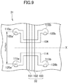
- FIG. 9 is a schematic view illustrating the flat surface of the portion of the printed circuit board according to the second embodiment of the present invention.
- FIG. 10 is a diagram illustrating characteristics of the differential transmission line according to the second embodiment of the present invention.
- FIG. 11 is a schematic view illustrating a flat surface of a portion of a printed circuit board according to a third embodiment of the present invention.
- FIG. 12 is a diagram illustrating characteristics of a differential transmission line according to the third embodiment of the present invention.
- FIG. 13 is a schematic view illustrating a structure of a portion of a printed circuit board according to a fourth embodiment of the present invention.
- FIG. 14 is a schematic view illustrating a structure of a portion of a printed circuit board according to a fifth embodiment of the present invention.
- FIG. 15 is a schematic view illustrating a structure of a portion of a printed circuit board according to a sixth embodiment of the present invention.
- FIG. 16 is a schematic view illustrating a structure of a portion of a printed circuit board according to a seventh embodiment of the present invention.
- FIG. 17 is a schematic view illustrating a cross section of the portion of the printed circuit board according to the seventh embodiment of the present invention.
- FIG. 18 is a schematic view illustrating a flat surface of a portion of a printed circuit board according to a comparative example of the first embodiment of the present invention.
- FIG. 19 is a diagram illustrating characteristics of a differential transmission line according to the comparative example of the first embodiment of the present invention.
- FIG. 1 is a schematic view illustrating a configuration of an optical transmission equipment 1 and an optical module 2 according to a first embodiment of the present invention.
- the optical transmission equipment 1 includes a printed circuit board 11 .
- the optical module 2 includes a printed circuit board 21 .
- the printed circuit board according to the first embodiment is one or both of the printed circuit boards 11 and 21 .
- the optical transmission equipment 1 further includes an IC 12 .
- the optical transmission equipment 1 is, for example, a large-capacity router or a switch.
- the optical transmission equipment 1 has, for example, a function of a switching equipment, and is disposed in a base station or the like.
- the optical transmission equipment 1 acquires data for receiving (electric signal for receiving) from the optical module 2 , determines to transmit what data to where using the IC 12 or the like, generates data for transmitting (electric signal for transmitting), and transmits the data to the corresponding optical module 2 through the printed circuit board 11 .
- the optical module 2 is a transceiver having a function of optical transmitting and a function of optical receiving, and includes a ROSA 23 A which converts an optical signal received through an optical fiber 3 A into an electric signal, and a TOSA 23 B which converts an electric signal to an optical signal and transmits the optical signal to an optical fiber 3 B.
- the printed circuit board 21 , the ROSA 23 A and the TOSA 23 B are connected to each other through flexible boards 22 A and 22 B (flexible printed circuit: FPC), respectively.
- An electric signal is transmitted from the ROSA 23 A to the printed circuit board 21 through the flexible board 22 A, and an electric signal is transmitted from the printed circuit board 21 to the TOSA 23 B through the flexible board 22 B.
- the optical modules 2 and the optical transmission equipment 1 are connected to each other through an electrical connector 5 .
- the ROSA 23 A and the TOSA 23 B are electrically connected to the printed circuit board 21 and are optical elements that convert from one to the other of optical signals or electric signals.
- a transmission system includes two or more of the optical transmission equipment 1 , two or more of the optical modules 2 , and one or more of optical fibers 3 .
- Each optical transmission equipment 1 is mounted on one or more of the optical modules 2 .
- the optical fiber 3 is connected between the optical modules 2 mounted on the two optical transmission equipments 1 , respectively.
- Transmission data generated by one of the optical transmission equipment 1 is converted into an optical signal by the mounted optical module 2 , and such an optical signal is transmitted to the optical fiber 3 .
- the optical signal transmitted over the optical fiber 3 is received by the optical module 2 mounted on the other optical transmission equipment 1 , and the optical module 2 converts the optical signal into an electric signal and transmits the electric signal to the other optical transmission equipment 1 as reception data.
- the bit rate of the electric signal transmitted and received by each of the optical modules 2 is 100 Gbit/s class, and the optical module 2 has a multi-channel system of 4 channels for transmitting and 4 channels for receiving.
- the bit rate of the electric signal transmitting each channel is any one of 25 Gbit/s to 28 Gbit/s, specifically, the bit rate of the electric signal transmitting each channel is 25.78 Gbit/s.
- a differential transmission line is a line for propagating an electrical serial data signal with a bit rate of 25.78 Gbit/s.
- FIG. 2 is a schematic view illustrating a flat surface of a portion of a printed circuit board 31 according to the first embodiment.
- FIG. 3 is a schematic view illustrating a cross section of the portion of the printed circuit board 31 according to the first embodiment.
- FIGS. 2 and 3 schematically illustrate the flat surface and the cross section, respectively, in order to understand the structure of the printed circuit board 31 , so that the actual plan view and sectional view are different from each other.
- the printed circuit board 31 is a printed wiring board having a multilayer structure in which a plurality of conductor layers are formed through each of dielectric layers, and in FIGS.
- FIG. 3 illustrates a cross section taken along line III-III illustrated in FIG. 2 .
- the printed circuit board 31 has a plurality of differential transmission lines for high speed digital signals, and the printed circuit board 31 has a plurality of channels.
- one differential transmission line 32 (one channel) among the plurality of differential transmission lines is illustrated.
- the bit rate of the electric signal transmitted to the differential transmission line 32 is 25.78 Gbit/s.
- the printed circuit board 31 is the printed circuit board 21 of the optical module 2 , but as described above, the printed circuit board 11 of the optical transmission equipment 1 may be used.
- the printed circuit board 31 is provided with a dielectric layer 100 , a pair of strip conductors 101 and 102 , a ground conductor layer 103 , a first resonator conductor 104 , and a pair of first via holes 105 a , and 105 b .
- a protective dielectric film 107 is disposed over the entire surface, in order to facilitate understanding of the multilayer structure of the printed circuit board 31 , the protective dielectric film 107 is omitted.
- the dielectric layer 100 is not illustrated in FIG. 2 .
- the dielectric layer 100 a material (glass epoxy resin) including a glass cloth substrate and an epoxy resin is used.
- the relative dielectric constant of the dielectric layer 100 is 3.5.
- the dielectric layer 100 includes the first resonator conductor 104 therein, and is disposed between the pair of strip conductors 101 and 102 and the ground conductor layer 103 .
- the pair of strip conductors 101 and 102 are disposed on the board surface side (upper side in FIG. 3 ) in the lamination orientation of the ground conductor layer 103 , and both extend along a first orientation (vertical orientation illustrated in FIG. 2 ).
- the pair of strip conductors 101 and 102 are formed on the uppermost metal layer of the multilayer structure of the printed circuit board 31 .
- the pair of strip conductors 101 and 102 are copper foils having a thickness of 37 ⁇ m.
- a width W of the pair of strip conductors 101 and 102 is 0.17 mm, and an interval G between the pair of strip conductors 101 and 102 is 0.20 mm.
- the interval G is the distance from the inner edge of the strip conductor 101 to the inner edge of the strip conductor 102 . It is desirable that the pair of strip conductors 101 and 102 are spaced apart from each other by the interval G, have the width W, and extend in a linear shape in the first orientation in parallel with each other.
- the shapes of the pair of strip conductors 101 and 102 may be bent or the like, depending on the relationship with other components mounted on the printed circuit board 31 . Even in such a case, in a region three-dimensionally intersecting with the first resonator conductor 104 and a region in the vicinity thereof, the shape may be a parallel linear shape.
- a planar shape of the pair of strip conductors 101 and 102 is processed and formed by patterning.
- the ground conductor layer 103 is a copper foil with a thickness of 18 ⁇ m and is a third metal layer counted from the front surface side among the multilayer structure of the printed circuit board 31 .
- the distance H 1 between the pair of strip conductors 101 and 102 and the ground conductor layer 103 is 166 ⁇ m.
- the distance H 1 between the pair of strip conductors 101 and 102 and the ground conductor layer 103 is the distance between the lower surface of the pair of strip conductors 101 , 102 and the upper surface of the ground conductor layer 103 .
- the differential transmission line 32 of a micro-strip line type, through which a digital modulation signal is transmitted is configured by the dielectric layer 100 , the pair of strip conductors 101 and 102 , and the ground conductor layer 103 .
- the characteristic impedance of the differential transmission line 32 in the differential mode can be made 100 ⁇ .
- the ground conductor layer 103 may have a shape including a region below the pair of strip conductors 101 and 102 and the first resonator conductor 104 and extending to both sides in the second orientation.
- the second orientation is an orientation intersecting the first orientation.
- the first resonator conductor 104 is disposed between the pair of strip conductors 101 and 102 and the ground conductor layer 103 .
- the first resonator conductor 104 is a copper foil with a thickness of 36 ⁇ m and is a second metal layer counted from the front surface side among the multilayer structure of the printed circuit board 31 . As illustrated in FIG. 3 , the distance H 2 between the pair of strip conductors 101 and 102 and the first resonator conductor 104 is 65 ⁇ m.
- the distance H 2 between the pair of strip conductors 101 and 102 and the first resonator conductor 104 is the distance between the lower surface of the pair of strip conductors 101 , 102 and the upper surface of the first resonator conductor 104 . It is desirable that the distance H 1 is twice or more the distance H 2 , and the printed circuit board 31 according to the first embodiment satisfies such a condition.
- the first resonator conductor 104 three-dimensionally intersects with the pair of strip conductors 101 and 102 along the second orientation. It is desirable that the angle between the first orientation and the second orientation is 85° or more and 90° or less, and it is further desirable that the first orientation and the second orientation are substantially orthogonal to each other (angle formed is 90°). In the first embodiment, the first orientation (vertical orientation in FIG. 2 ) and the second orientation (horizontal orientation in FIG. 2 ) are orthogonal to each other.
- the first resonator conductor 104 is provided with land portions 110 a and 110 b (via lands) each having a circular shape (diameter: 0.45 mm) at both ends thereof.
- the pair of first via holes 105 a and 105 b are respectively disposed so that the center of the circular shape is ideally penetrated through the center of the circular shape of the land portions 110 a and 110 b .
- Each of the pair of first via holes 105 a and 105 b is a cylindrical through hole having a diameter of 0.20 mm, and a metal is disposed on the inner wall of the through hole.
- the distance D between the centers of the pair of first via holes 105 a and 105 b is 2.0 mm.
- a circular hole (through hole) is formed in the dielectric layer 100 by a drill step so as to extend from the pair of strip conductors 101 and 102 (uppermost metal layer) to the ground conductor layer 103 (third metal layer) perpendicular to the planar direction of the printed circuit board 31 , and the pair of first via holes 105 a and 105 b are formed by copper plating in the inner wall (inside surface) of the hole.
- the pair of first via holes 105 a and 105 b connect the first resonator conductor 104 (land portions 110 a and 110 b at the both ends of) and the ground conductor layer 103 , respectively.
- a first resonator structure is configured to include the ground conductor layer 103 , the first resonator conductor 104 , and the pair of first via holes 105 a and 105 b.
- the protective dielectric film 107 is the uppermost layer of the printed circuit board 31 and is disposed so as to cover the pair of strip conductors 101 and 102 and the dielectric layer 100 .
- the protective dielectric film 107 is a dielectric film called a solder resist for preventing adhesion of solder and has a thickness of approximately 40 ⁇ m.
- the protective dielectric film 107 may not be disposed unless otherwise required.
- the first feature of the printed circuit board 31 according to the first embodiment lies in the shape of the first resonator conductor 104 .
- the second feature is that the distance H 1 is twice or more the distance H 2 .
- the shape of the first resonator conductor 104 will be described.
- the planar shape of the first resonator conductor 104 is processed and formed by patterning.
- the first resonator conductor 104 extends in a linear shape from each of (centers of) the land portions 110 a and 110 b at both ends along the second orientation to the inside of the first resonator conductor 104 . That is, the first resonator conductor 104 extends from each of (centers of) the pair of first via holes 105 a and 105 b along the second orientation to the inside of the first resonator conductor 104 .
- the description of “to extend to the inside of the first resonator conductor 104 ” means to extend in an orientation approaching from both sides with respect to the pair of strip conductors 101 and 102 with which the first resonator conductor 104 three-dimensionally intersects.
- the description of “to extend to the outside of the first resonator conductor 104 ” means to extend in an orientation away from both sides with respect to the pair of strip conductors 101 and 102 with which the first resonator conductor 104 three-dimensionally intersects.
- the planar shape of the first resonator conductor 104 and the pair of first via holes 105 a and 105 b are formed in separate steps, so that the positional deviation occurs between (centers of) the land portions 110 a and 110 b and (centers of) the pair of the first via holes 105 a and 105 b , respectively.
- the positional deviation amount is 0.125 mm.
- the diameter 0.45 mm of the land portions 110 a and 110 b is a value that can correspond to the diameter 0.20 mm of the pair of first via holes 105 a and 105 b and the positional deviation amount of 0.125 mm.
- the width W 1 of the portion extending in a linear shape (excluding the bent portion) is 0.20 mm.
- first resonator conductor 104 extends along the second orientation from each of the land portions 110 a and 110 b or from each of the pair of first via holes 105 a and 105 b ” allows a tolerance in positional deviation on manufacturing, so that the center of the linear shape portion of the first resonator conductor 104 may not strictly extend from the center of the land portions 110 a and 110 b , and the extending orientation of the linear shape may be along the second orientation and may not be strictly parallel to the second orientation.
- the description of “along the first orientation (or the second orientation)” is the same.
- both of the first resonator conductor 104 extend along the second orientation from both ends thereof (land portions 110 a and 110 b ) or from each of the pair of first via holes 105 a and 105 b to the inside of the first resonator conductor 104 , and that both further bend in any one direction in the first orientation (downward in FIG. 2 ). Furthermore, it is desirable that both extend to the inside of the first resonator conductor 104 along the second orientation, and reach the portions three-dimensionally intersecting with the pair of strip conductors 101 and 102 .
- the first resonator conductor 104 extends to the outside along the second orientation from the portions three-dimensionally intersecting with the pair of strip conductors 101 and 102 , bends in any one direction in the first orientation (upward in FIG. 2 ), further extends along the first orientation, bends to the outside in the second orientation, and extends to the outside along the second orientation to connect with the pair of first via holes.
- the first resonator conductor 104 has a shape extending to the inside along the second orientation from the land portions 110 a and 110 b disposed at both ends thereof. Since the first resonator conductor 104 has such a shape, it is possible to suppress degradation of characteristics due to the positional deviation between the land portions 110 a and 110 b and the pair of first via holes 105 a and 105 b . Details of the effect will be described later.
- the first resonator conductor 104 has a shape connected to the pair of strip conductors 101 and 102 extending along the first orientation, and to the land portions 110 a and 110 b which three-dimensionally intersect along the second orientation, respectively extend along the second orientation from a portion three-dimensionally intersects, repeat bending and stretching, and are disposed at both ends thereof. Since the first resonator conductor 104 according to the first embodiment has such a shape, a line length L of the first resonator conductor 104 from the center position of one via hole (for example, via hole 105 a ) of the pair of first via holes to the center position of the other via hole (for example, via hole 105 b ) is 3.4 mm.
- the line length L is the length of the center line of the linear shape in which the first resonator conductor extends, and in the bent portion, the line length L may be calculated based on the center line of the linear shape respectively extending to both sides.
- the length Li of the center line of the linear shape portion extending in the first orientation of the first resonator conductor 104 is 0.7 mm. That is, considering the center line, it is possible to dispose the first resonator conductor 104 having a long line length of 3.4 mm in a small region of 0.7 mm along the first orientation.
- the first resonator conductor 104 is disposed inside the dielectric layer 100 having a relative dielectric constant ⁇ r of 3.5, and a wavelength shortening ratio (1/ ⁇ r ) of the dielectric layer 100 with respect to a vacuum is 0.535.
- One wavelength ⁇ g of the first resonator conductor 104 at a frequency of 25.78 GHz corresponding to the bit rate is calculated to be 6.22 mm. Therefore, the line length L of 3.4 mm of the first resonator conductor 104 is 0.55 ⁇ g in terms of the wavelength ⁇ g.
- an appropriate value of the line length L of the first resonator conductor 104 may be selected according to the case.
- the appropriate value can be obtained by, for example, an electromagnetic field analysis tool, and desirably has a length of 0.4 wavelength or more and 0.6 wavelength or less at a frequency corresponding to the bit rate of the digital modulation signal.
- the bit rate is 25.78 Gbit/s
- the frequency corresponding to the bit rate is 25.78 GHz. That is, the frequency corresponding to the bit rate of the digital modulation signal is obtained by changing the unit to Hz with the numerical value of the bit rate (unit bit/s) unchanged.
- the first resonator conductor 104 has a shape that is substantially line symmetrical with respect to the pair of strip conductors 101 and 102 in a plan view.
- the description of “to be line symmetrical with respect to the pair of strip conductors 101 and 102 ” means to be line symmetrical with respect to the center line of the pair of strip conductors 101 and 102 (center line of the strip conductor 101 and center line of the strip conductor 102 ). It is desirable to reduce the influence on the conduction propagation of the differential signal component transmitted to the differential transmission line. Therefore, it is desirable that the resonator structure is symmetrical with respect to the pair of strip conductors 101 and 102 .
- FIG. 4 is a diagram illustrating characteristics of a differential transmission line 32 according to the first embodiment.
- FIG. 4 is a graph illustrating the frequency dependence of the differential mode pass characteristic (Sdd21), differential mode reflection characteristic (Sdd11 and Sdd22), and common mode pass characteristic (Scc21) in the differential transmission line 32 . Since the first resonator conductor 104 (first resonator structure) three-dimensionally intersects with the pair of strip conductors 101 and 102 (differential transmission line 32 ), deterioration (increase) occurs in the differential mode reflection characteristic (Sdd 11 and Sdd 22), but it is a value of ⁇ 20 dB or less in the frequency range of 0 to 30 GHz, and a relatively favorable value is maintained.
- the first resonator conductor 104 has a narrow linear shape with a width W 1 of 0.20 mm, and the area which three-dimensionally intersects with the pair of strip conductors 101 and 102 (facing area, and overlapping area in a plan view) is reduced.
- the differential mode pass characteristic (Sdd 21) illustrates favorable characteristics.
- the common mode pass characteristic (Scc 21) an attenuation region centered at the frequency 26.3 GHz is generated, and conduction propagation of the common mode signal component of the frequency 25.78 GHz can be inhibited by approximately 10 dB.
- FIG. 18 is a schematic view illustrating a flat surface of a portion of a printed circuit board 331 according to a comparative example of the first embodiment.
- FIG. 19 is a diagram illustrating characteristics of a differential transmission line 32 according to the comparative example, and illustrates the common mode pass characteristic (Sec 21 ) in a case where the positional deviation ⁇ y is +0.125 mm, 0, and ⁇ 0.125 mm, respectively.
- the printed circuit board 331 according to the comparative example has the same structure except that the shape of the first resonator conductor 304 is different from the shape of the first resonator conductor 104 according to the first embodiment.
- the first resonator conductor 304 extends along any one direction in the first orientation (downward as illustrated in FIG. 18 ) from land portions 310 a and 310 b disposed at the both ends, extends to the inside of the first resonator conductor 304 along the second orientation, and reaches the portion that three-dimensionally intersects with the pair of strip conductors 101 and 102 .
- the distance D between the centers of the pair of first via holes 105 a and 105 b is 1.4 mm
- the line length L of the first resonator conductor 304 from the center position of the via hole 105 a to the center position of the via hole 105 b is 3.2 mm.
- the characteristics of a differential transmission line 332 are similar to the characteristics of the differential transmission line 32 illustrated in FIG. 4 .
- the pair of first via holes 105 a and 105 b having the positional deviation amount of 0.125 mm may vary by ⁇ 0.125 mm maximum with respect to the first resonator conductor 104 (or 304 ) in each of the first orientation and the second orientation.
- the relative position between the first resonator conductor 104 (or 304 ) and the pair of first via holes 105 a and 105 b varies.
- the planar shape of the first resonator conductor 104 is formed by patterning, the relative positional variations of the land portions 110 a and 110 b (or 310 a and 310 b ) of the first resonator conductor 104 (or 304 ) are significantly small.
- the pair of first via holes 105 a and 105 b are formed by a common drilling step, the relative positional variations (distance D between the centers) of the pair of first via holes 105 a and 105 b are significantly small.
- the positional deviation ⁇ y of the pair of first via holes 105 a and 105 b (each center position) with respect to the land portions 310 a and 310 b (each center position) along the first orientation (vertical orientation illustrated in FIG. 18 ) will be considered.
- the line length L varies according to the positional deviation ⁇ y along the first orientation.
- the line length L of the first resonator conductor 304 significantly varies depending on the positional deviation ⁇ y. That is, the differential transmission line 332 according to the comparative example is significantly affected by the positional deviation along the first orientation between the first resonator conductor 304 and the pair of first via holes 105 a and 105 b . As illustrated in FIG.
- the center frequency of the attenuation region in the common mode passing characteristic (Sec 21 ) significantly varies up and down to 3.6 GHz. Therefore, in the differential transmission line 332 according to the comparative example 1, it is found that it is difficult to inhibit the conduction propagation of the common mode signal component of the frequency (25. 78 GHz) corresponding to the bit rate of the digital modulation signal by the first resonator structure due to the manufacturing variation.
- the first resonator conductor 104 according to the first embodiment extends in a linear shape to the inside of the first resonator conductor 104 along the second orientation from each of (centers of) the land portions 110 a and 110 b at both ends. Therefore, in the pair of first via holes 105 a and 105 b (each of the center positions), even in a case where the positional deviation ⁇ y with respect to the land portions 110 a and 110 b (each of the center positions) along the first orientation (vertical orientation illustrated in FIG. 2 ) occurs, the variation of the line length L of the first resonator conductor 104 according to the first embodiment is suppressed.
- the variation of the center frequency of the attenuation region in the common mode pass characteristic (Scc 21) of the differential transmission line 32 according to the first embodiment due to the positional deviation ⁇ y is significantly small compared to the variation of the differential transmission line 332 according to the comparative example.
- the length of the center line along the first orientation on the side of the via hole 105 a decreases depending on the positional deviation amount, but the length of the center line along the first orientation on the side of the via hole 105 b increases depending on the positional deviation amount, and the variation of the line length L is significantly small. Therefore, the variation of the center frequency of the attenuation region in the common mode pass characteristic (Sec 21 ) of the differential transmission line 32 according to the first embodiment is significantly small.
- the variation of the line length L of the first resonator conductor 304 according to the comparative example is small, similar to the positional deviation ⁇ y along the first orientation of the first resonator conductor 104 according to the first embodiment.
- the differential transmission line 32 it is possible to selectively inhibit the conduction propagation of the common mode signal component to the differential transmission line 32 while suppressing deterioration of the conduction propagation of the differential signal component. That is, substantially, only the conduction propagation of the common mode signal component to the differential transmission line can be selectively inhibited.
- an additional step is not required, and an increase in manufacturing cost is suppressed.
- the shape of the first resonator conductor 104 according to the first embodiment is bent, the region where the first resonator conductor 104 is disposed can be reduced, and the first resonator conductor 104 can be disposed at a high density.
- the dielectric layer 100 according to the first embodiment is formed using a material including a glass cloth substrate and an epoxy resin (glass epoxy resin), it is not limited to this material, and may be a liquid crystal polymer (LCP) or a fluorine-based resin (Polytetrafluoroethylene: PTFE).
- LCP liquid crystal polymer
- PTFE fluorine-based resin
- the optical module optical transceiver and optical transceiver module
- speeding up, downsizing, and cost reduction is achieved, with the spread of broadband network in recent years, and regarding speeding up, currently the optical module having a bit rate of 100 Gbit/s are widely used.
- the housing (case) volume is reduced and the number of parts is reduced from the CFP Multi Source Agreement (MSA) standard to CFP 2, CFP 4, and QSFP 28 (each MSA standard).
- MSA CFP Multi Source Agreement
- the optical transmission equipment network equipment on which the optical module is mounted
- it is required to suppress the intensity of unnecessary electromagnetic waves generated by the equipment to a limit value defined by law or regulations.
- a limit value defined by law or regulations.
- it is required to reduce the intensity of unnecessary electromagnetic waves below the limit value of 53.9 dB ( ⁇ V/m) specified in “FCC Part 15 Subpart B” standard (in a case where distance is 3 m, and frequency range is 1 GHz to 40 GHz in Class B standard).
- unnecessary electromagnetic waves at high frequency are generated in many cases due to switching noises or the like of built-in IC. Therefore, a design technique for reducing radiation of the unnecessary electromagnetic waves to the outside of the equipment is important in both the optical transmission equipment and the optical module.
- the main excitation source of unnecessary electromagnetic waves is an IC (such as CDR, Driver, TIA, and the like) that amplifies and outputs an electrical serial data signal (modulation signal).
- the ideal serial data signal does not include repetitive signal patterns, so that it does not have a large peak intensity on the frequency spectrum.
- switching noise is generated due to nonlinearity of the transistor. Therefore, in a case of observing the frequency spectrum of the common mode component of the output signal, a large peak occurs at the frequency corresponding to the bit rate.
- the common mode signal component While conducting and propagating through the differential transmission line on the printed circuit board, the common mode signal component propagates to space as a part thereof as radiation loss.
- LSI FPGA
- heat generation amount power consumption
- a large number of ventilation holes are disposed to strengthen air blowing cooling, and the shielding effect of the equipment tends to be low.
- a plurality of optical modules of 100 Gbit/s class are mounted on the optical transmission equipment.
- an external connection terminal is disposed on one end of the printed circuit board, and the external connection terminal is connected to a connector mounted on the optical transmission equipment outside the metal housing.
- the printed circuit board 31 according to the first embodiment has a structure suitable for solving such a problem.
- FIG. 5 is a schematic perspective view illustrating an external shape of an optical module 2 according to the first embodiment.
- FIG. 6 is a schematic perspective view illustrating the structure of the optical module 2 according to the first embodiment.
- FIG. 6 illustrates a state where the optical module 2 is mounted on the optical transmission equipment 1 .
- the printed circuit board 31 according to the first embodiment is the printed circuit board 21 here.
- the optical module 2 is the optical module conforming to the QSFP (MSA standard). As illustrated in FIG. 5 , the optical module 2 includes an upper case 200 , a lower case 201 , a latch 202 , and a card edge connector 210 .
- Metal such as zinc or aluminum is used as the material of the upper case 200 and the lower case 201 , and a metal housing is configured to include the upper case 200 and the lower case 201 .
- the upper case 200 and the lower case 201 configure an electromagnetic shield by covering the printed circuit board 21 in close contact with each other so that there are no gaps in a portion other than the opening portion for passing the card edge connector 210 .
- the metal housing (upper case 200 and lower case 201 ) functions as an electromagnetic shield against the radiation from the printed circuit board 21 inside the metal housing.
- the metal housing has the opening portion, the metal housing functions sufficiently as the electromagnetic shield.
- the metal housing has no function of preventing conduction propagation of unnecessary noise components contained in the output signal from the optical module to the optical transmission equipment. As a result, unnecessary electromagnetic waves caused by unnecessary noise components conducted and propagated to the differential transmission line drawn out to outside of the metal housing through the opening portion and the connector portion can be radiated to outside of the metal housing.
- the card edge connector 210 is an end portion of the printed circuit board 21 , and a plurality of contact terminals for connecting the connector are disposed in a row.
- the card edge connector 210 is exposed to the outside from the opening portion (slot opening portion) on the rear sides (right side in FIG. 5 ) of the upper case 200 and the lower case 201 , and has the function of hot swapping.
- the opening portion is provided to expose a portion of the printed circuit board 21 to the outside.
- FIG. 6 illustrates a state where the optical module 2 is mounted on the optical transmission equipment 1 , and in order to illustrate the internal structure of the optical module 2 , a portion of the upper case 200 and the lower case 201 is not illustrated.
- a portion of the printed circuit board 11 and a front panel 204 inside the optical transmission equipment 1 are illustrated.
- a printed circuit board 11 further includes the connector 208 conforming to the QSFP 28 (MSA standard), and the connector 208 is mounted on the printed circuit board 11 .
- ROSA 23 A (receiver optical subassembly), TOSA 23 B (transmitter optical subassembly: not illustrated), and flexible boards 22 A and 22 B ( 22 B not illustrated) are mounted inside of the upper case 200 and the lower case 201 of the optical module 2 .
- the printed circuit board 21 includes a plurality of ICs.
- a Clock Data Recovery IC (CDR-IC) 207 on the receiving side is mounted on the printed circuit board 21 , and the CDR-IC 207 outputs the 4-channel differential digital modulation signal at a bit rate of 25.78 Gbit/s.
- CDR-IC Clock Data Recovery IC
- the output signal is conducted and propagated to the printed circuit board 11 inside the optical transmission equipment 1 through the four pairs of differential transmission lines 32 (not illustrated) disposed on the printed circuit board 21 , the card edge connector 210 , and the connector 208 .
- the first resonator structure illustrated in FIG. 2 is disposed in each of the four pairs of differential transmission lines 32 disposed on the printed circuit board 21 .
- the first resonator structure illustrated in FIG. 2 is disposed in each of the four pairs of differential transmission lines 32 , so that the conduction propagation of the common mode signal component at the frequency of 25.78 GHz can be inhibited inside the upper case 200 and the lower case 201 of the optical module 2 . Therefore, in the card edge connector 210 , the connector 208 , and the printed circuit board 11 of the optical transmission equipment 1 , radiation of unnecessary electromagnetic waves caused by the common mode signal component can be reduced. Similarly to this mechanism, the first resonator structure illustrated in FIG.
- the CDR-IC 207 for receiving is disposed on the printed circuit board 21 , but it is not limited thereto, and may be mounted in the inside of the ROSA 23 A. In this case, since it is not required to dispose the CDR-IC 207 on the printed circuit board 21 , the area for disposing the first resonator conductor 104 illustrated in FIG. 2 on the printed circuit board 21 can be widely allocated to each of the four pairs of differential transmission lines, and the degree of freedom of circuit design of the printed circuit board 21 is improved.
- FIG. 7 is a schematic view illustrating a flat surface of a portion of a printed circuit board 31 according to a second embodiment of the present invention.
- FIG. 8 is a diagram illustrating characteristics of a differential transmission line 32 according to the second embodiment.
- FIG. 8 illustrates the common mode pass characteristic (Scc 21) of the differential transmission line 32 according to the second embodiment, and the common mode pass characteristic (Scc 21) of the differential transmission line 32 according to the first embodiment of the present invention for comparison.
- the printed circuit board 31 according to the second embodiment is different from the first embodiment in that the printed circuit board 31 further includes a second resonator conductor 114 and second via holes 115 a and 115 b in addition to the first resonator conductor 104 , the other structure is the same as that of the first embodiment.
- the second resonator conductor 114 is disposed in the same layer (second metal layer) as the first resonator conductor 104 , and is provided with circular land portions 120 a and 120 b at both ends thereof.
- the second resonator conductor 114 is disposed side by side with the first resonator conductor 104 along the first orientation (vertical orientation in FIG. 7 ), and the planar shape of the second resonator conductor 114 is substantially line symmetric with the plane shape of the first resonator conductor 104 with respect to the straight line X illustrated in FIG. 7 .
- the second resonator conductor 114 extends to the outside along the second orientation in parallel with the first resonator conductor 104 from the portions three-dimensionally intersecting with the pair of strip conductors 101 and 102 , bends in the other direction in the first orientation (downward in FIG. 2 ), further extends away from the first resonator conductor 104 along the first orientation, bends to the outside in the second orientation, and extends to the outside along the second orientation to connect the pair of second via holes 115 a and 115 b .
- the pair of second via holes 115 a and 115 b are respectively disposed so that the center of the circular shape is ideally penetrated through the center of the circular shape of the land portions 120 a and 120 b .
- the pair of second via holes 115 a and 115 b connects (land portions 120 a and 120 b at the both ends of) the second resonator conductor 114 and the ground conductor layer 103 , respectively.
- the second resonator structure is configured to include the ground conductor layer 103 , the second resonator conductor 114 , and the pair of second via holes 115 a and 115 b.
- the distance between the centers (Via Pitch) between one first via hole (via hole 105 a ) of the pair of first via holes and one second via hole (via hole 115 a ) of the pair of second via holes disposed along the first orientation is changed. Therefore, the attenuation characteristic in the common mode pass characteristic can be adjusted.
- the distance between the centers (Via Pitch) is set to 2.2 mm.
- the distance is not limited to this value, and the distance may be set to an appropriate value according to the attenuation characteristic in the common mode pass characteristic.
- the attenuation region centered at a frequency of 26.3 GHz is generated, and conduction propagation of the common mode signal component of the frequency of 25.78 GHz can be inhibited by approximately 20 dB.
- the common mode pass characteristic (Scc 21) of the differential transmission line 32 according to the first embodiment of the present invention achieves greater attenuation, and the frequency range that can inhibit the conduction propagation of the common mode signal component can be widened.
- FIG. 9 is a schematic view illustrating the flat surface of the portion of the printed circuit board 31 according to the second embodiment of the present invention.
- FIG. 10 is a diagram illustrating characteristics of the differential transmission line 32 according to the second embodiment.
- FIG. 9 illustrates a case where the positional deviation ⁇ y occurs with respect to the land portions 110 a and 110 b and the land portions 120 a and 120 b in any one direction of the first orientation (downward as illustrated in FIG. 9 ) in the pair of first via holes 105 a and 105 b and the pair of second via holes 115 a and 115 b in the printed circuit board 31 illustrated in FIG. 7 .
- the positional deviation ⁇ y is ⁇ 0.125 mm.
- FIG. 11 is a schematic view illustrating a flat surface of a portion of a printed circuit board 31 according to a third embodiment of the present invention.
- FIG. 12 is a diagram illustrating characteristics of a differential transmission line 32 according to the third embodiment.
- FIG. 12 illustrates the common mode pass characteristic (Scc 21) of the differential transmission line 32 according to the third embodiment, and the common mode pass characteristic (Scc 21) of the differential transmission line 32 according to the first embodiment of the present invention for comparison.
- the shape of the second resonator conductor 114 is different from that of the second embodiment, the other structure is the same as that of the second embodiment.
- the planar shape of the second resonator conductor 114 is substantially line symmetric with the plane shape of the first resonator conductor 104 with respect to the straight line X illustrated in FIG. 7 , whereas in the third embodiment, the planar shape of the second resonator conductor 114 substantially coincides with the one obtained by translating the planar shape of the first resonator conductor 104 in any one direction of the first orientation (downward in FIG. 11 ).
- the second resonator conductor 114 extends to the outside along the second orientation in parallel with the first resonator conductor 104 from the portions three-dimensionally intersecting with the pair of strip conductors 101 and 102 , bends in any one direction of the first orientation (downward in FIG.
- the pair of second via holes 115 a and 115 b (circular shape) are respectively disposed so that the center of the circular shape is ideally penetrated through the center of the circular shape of the land portions 120 a and 120 b .
- the pair of second via holes 115 a and 115 b connects (land portions 120 a and 120 b at the both ends of) the second resonator conductor 114 and the ground conductor layer 103 , respectively.
- the second resonator structure is configured to include the ground conductor layer 103 , the second resonator conductor 114 , and the pair of second via holes 115 a and 115 b.
- the distance between the centers (Via Pitch) between one first via hole (via hole 105 a ) of the pair of first via holes and one second via hole (via hole 115 a ) of the pair of second via holes disposed along the first orientation is changed. Therefore, the attenuation characteristic in the common mode pass characteristic can be adjusted.
- the distance between the centers (Via Pitch) is set to 1.2 mm.
- the distance is not limited to this value, and the distance may be set to an appropriate value according to the attenuation characteristic in the common mode pass characteristic.
- the first resonator conductor 104 and the second resonator conductor 114 are disposed on the printed circuit board 32 according to the third embodiment, a wider region is required for disposing two resonator conductors.
- the attenuation region centered at a frequency of 26.3 GHz is generated, and conduction propagation of the common mode signal component of the frequency of 25.78 GHz can be inhibited by approximately 20 dB.
- the common mode pass characteristic (Scc 21) of the differential transmission line 32 according to the first embodiment of the present invention achieves greater attenuation, and the frequency range that can inhibit the conduction propagation of the common mode signal component can be widened.
- FIG. 13 is a schematic view illustrating a structure of a portion of a printed circuit board 31 according to a fourth embodiment of the present invention.
- the shape of the first resonator conductor 104 is different from that of the first embodiment, the other structure is the same as that of the first embodiment.
- the first resonator conductor 104 according to the first embodiment extends in a linear shape from each of (centers of) the land portions 110 a and 110 b at both ends along the second orientation to the inside of the first resonator conductor 104
- the first resonator conductor 104 according to the fourth embodiment extends in a linear shape from each of (centers of) the land portions 110 a and 110 b at both ends along the second orientation to the outside of the first resonator conductor 104
- the first resonator conductor 104 according to the fourth embodiment extends from each of (centers of) the pair of first via holes 105 a and 105 b along the second orientation to the outside of the first resonator conductor 104 .
- first extending direction and a second extending direction When the directions respectively extending from both ends of the first resonator conductor 104 extends are referred to as a first extending direction and a second extending direction, and in the first to third embodiments (and the fifth to seventh embodiments), the first extending direction and the second extending direction are opposed to each other on a straight line, and the angle between the first extending direction and the second extending direction is 180°. In the fourth embodiment, the first extending direction and the second extending direction tend to separate from each other on the straight line, and the angle between the first extending direction and the second extending direction is 180°.
- the first extending direction and the second extending direction may be either opposed to each other (facing inward) or separate away from each other (facing outward) along the second direction, and in either case, it is possible to reduce the variation of the line length L with respect to the positional deviation ⁇ x along the second orientation.
- both of the first resonator conductor 104 extend along the second orientation from both ends thereof (land portions 110 a and 110 b ) or from each of the pair of first via holes 105 a and 105 b to the outside of the first resonator conductor 104 , and that both further bend in any one direction in the first orientation (downward in FIG. 13 ). Furthermore, it is desirable that both extend to the inside of the first resonator conductor 104 along the second orientation, and reach the portions three-dimensionally intersecting with the pair of strip conductors 101 and 102 .
- the first resonator conductor 104 extends to the outside along the second orientation from the portions three-dimensionally intersecting with the pair of strip conductors 101 and 102 , bends in any one direction in the first orientation (upward in FIG. 2 ), further extends along the first orientation, bends to the inside in the second orientation, and extends to the inside along the second orientation to connect with the pair of first via holes.
- the distance D between the centers of the pair of first via holes 105 a and 105 b is 1.1 mm and the width W 1 of the first resonator conductor 104 is 0.20 mm.
- the first resonator conductor 104 has a linear shape portion to be extended and a bending portion, for impedance matching, the corner of the bending portion has a cut off shape.
- the length Li of the center line is 0.45 mm. Even with the printed circuit board 31 according to the fourth embodiment, the same effects as those of the first embodiment is achieved.
- FIG. 14 is a schematic view (perspective view) illustrating a structure of a portion of a printed circuit board 31 according to a fifth embodiment of the present invention.
- the shape of the first resonator conductor 104 is different from that of the first embodiment, the other structure is the same as that of the first embodiment.
- the first resonator conductor 104 according to the first embodiment has the bending portion, whereas the first resonator conductor 104 according to the fifth embodiment extends in a linear shape to the inside of the first resonator conductor 104 from both (centers of) the land portions 110 a and 110 b at both ends along the second orientation, and reaches the portions three-dimensionally intersecting with the pair of strip conductors 101 and 102 . That is, it is desirable that the first resonator conductor 104 extends to the outside along the second orientation from the portions three-dimensionally intersecting with the pair of strip conductors 101 and 102 to connect with the pair of first via holes.
- the first resonator conductor 104 extends in a linear shape except for the land portions 110 a and 110 b on both sides.
- the distance between the centers D between the pair of first via holes 105 a and 105 b is 3.05 mm.
- the width W 1 of the first resonator conductor 104 is 0.19 mm.
- FIG. 15 is a schematic view (perspective view) illustrating a structure of a portion of a printed circuit board 31 according to a sixth embodiment of the present invention.
- the shape of the first resonator conductor 104 and the shape of the second resonator conductor 114 are different from these of the second and third embodiment, the other structure is the same as these of the second and third embodiment.
- Each of the first resonator conductor 104 and the second resonator conductor 114 according to the second and third embodiments has the bending portion, whereas each of the first resonator conductor 104 and the second resonator conductor 114 according to the sixth embodiment extends in a linear shape to the inside of the first resonator conductor 104 from each of the land portions at both ends along the second orientation, and reaches the portions three-dimensionally intersecting with the pair of strip conductors 101 and 102 .
- first resonator conductor 104 and the second resonator conductor 114 extend to the outside along the second orientation from the portions three-dimensionally intersecting with the pair of strip conductors 101 and 102 to connect with the pair of first via holes and the pair of second via holes.
- the first resonator conductor 104 and the second resonator conductor 114 extend in a linear shape except for the land portions on both sides.
- the distance between the centers D between the pair of first via holes 105 a and 105 b and the distance between the centers D between the pair of second via holes 115 a and 115 b are both 3.05 mm.
- the width W 1 of the first resonator conductor 104 is 0.19 mm.
- FIG. 16 is a schematic view (perspective view) illustrating a structure of a portion of a printed circuit board 31 according to a seventh embodiment of the present invention.
- FIG. 17 is a schematic view illustrating a cross section of the portion of the printed circuit board 31 according to the seventh embodiment.
- the shapes of the first resonator conductor 104 and the pair of first via holes 105 a and 105 b are different from these of the fifth embodiment, the other structure is the same as that of the fifth embodiment.
- the planar shape of the first resonator conductor 104 according to the seventh embodiment coincides with the planar shape of the first resonator conductor 104 according to the fifth embodiment, as illustrated in FIG. 17 , in the multilayer structure of the printed circuit board 31 , the first resonator conductor 104 according to the seventh embodiment is disposed in the uppermost metal layer, and the pair of strip conductors 101 and 102 according to the seventh embodiment are disposed in the second metal layer. That is, the first resonator conductor 104 is disposed on the board surface side in the lamination orientation of the ground conductor layer 103 , and the pair of strip conductors 101 and 102 are disposed between the first resonator conductor 104 and the ground conductor layer 103 .
- the first resonator conductor 104 is disposed on the board surface side in the lamination orientation of the pair of strip conductors 101 and 102 .
- the pair of first via holes 105 a and 105 b connects (land portions 110 a and 110 b at both ends of) the first resonator conductor 104 and the ground conductor layer 103 , respectively.
- the distance H 1 between the pair of strip conductors 101 and 102 and the ground conductor layer 103 is 138 ⁇ m
- the distance H 2 between the pair of strip conductors 101 and 102 and the first resonator conductor 104 is 65 ⁇ m.
- the distance H 1 is desirably twice or more the distance Hz, and the printed circuit board 31 according to the seventh embodiment satisfies such a condition.
- the width W of the pair of strip conductors 101 and 102 is 0.20 mm
- the interval G between the pair of strip conductors 101 and 102 is 0.20 mm.
- the distance between the centers D of the pair of first via holes 105 a and 105 b is 3.05 mm
- the width W 1 of the first resonator conductor 104 is 0.19 mm.
- the printed circuit board 31 according to the seventh embodiment has the same effects as that of the first embodiment.
- the configuration in which the first resonator conductor 104 and the second resonator conductor 114 are disposed further above the pair of strip conductors 101 and 102 is not limited to the seventh embodiment, and may be applied to each of the second to sixth embodiments.
- the printed circuit board, the optical module, and the optical transmission equipment are described.
- the present invention is not limited to the above embodiments and may be widely applied to a printed circuit board having a resonator structure and a differential transmission line of a micro-strip line type.
- the printed circuit board according to the present invention is the printed circuit board provided in the optical transmission equipment and the optical module, the printed circuit board may be provided in another equipment.
- the bit rate of the digital electric signal transmitted through each channel is 25.78 Gbit/s is described, it is not limited to such a bit rate and is suitable for a further higher bit rate.
Landscapes
- Physics & Mathematics (AREA)
- Engineering & Computer Science (AREA)
- Electromagnetism (AREA)
- Microelectronics & Electronic Packaging (AREA)
- General Physics & Mathematics (AREA)
- Optics & Photonics (AREA)
- Computer Networks & Wireless Communication (AREA)
- Signal Processing (AREA)
- Structure Of Printed Boards (AREA)
- Control Of Motors That Do Not Use Commutators (AREA)
Abstract
Description
-
- (1) to (4), the first resonator conductor may have a shape that is substantially line symmetric with respect to the pair of strip conductors in a plan view.
Claims (20)
Priority Applications (1)
| Application Number | Priority Date | Filing Date | Title |
|---|---|---|---|
| US16/796,040 US11224120B2 (en) | 2016-12-19 | 2020-02-20 | Print circuit board, optical module, and optical transmission equipment |
Applications Claiming Priority (2)
| Application Number | Priority Date | Filing Date | Title |
|---|---|---|---|
| JP2016245394A JP6784586B2 (en) | 2016-12-19 | 2016-12-19 | Printed circuit boards, optical modules, and optical transmission equipment |
| JP2016-245394 | 2016-12-19 |
Related Child Applications (1)
| Application Number | Title | Priority Date | Filing Date |
|---|---|---|---|
| US16/796,040 Continuation US11224120B2 (en) | 2016-12-19 | 2020-02-20 | Print circuit board, optical module, and optical transmission equipment |
Publications (2)
| Publication Number | Publication Date |
|---|---|
| US20180177042A1 US20180177042A1 (en) | 2018-06-21 |
| US10609812B2 true US10609812B2 (en) | 2020-03-31 |
Family
ID=62562903
Family Applications (2)
| Application Number | Title | Priority Date | Filing Date |
|---|---|---|---|
| US15/835,532 Active 2038-02-16 US10609812B2 (en) | 2016-12-19 | 2017-12-08 | Printed circuit board, optical module, and optical transmission equipment |
| US16/796,040 Active 2038-02-02 US11224120B2 (en) | 2016-12-19 | 2020-02-20 | Print circuit board, optical module, and optical transmission equipment |
Family Applications After (1)
| Application Number | Title | Priority Date | Filing Date |
|---|---|---|---|
| US16/796,040 Active 2038-02-02 US11224120B2 (en) | 2016-12-19 | 2020-02-20 | Print circuit board, optical module, and optical transmission equipment |
Country Status (3)
| Country | Link |
|---|---|
| US (2) | US10609812B2 (en) |
| JP (1) | JP6784586B2 (en) |
| CN (1) | CN108206318B (en) |
Cited By (1)
| Publication number | Priority date | Publication date | Assignee | Title |
|---|---|---|---|---|
| US11224120B2 (en) * | 2016-12-19 | 2022-01-11 | Lumentum Japan, Inc. | Print circuit board, optical module, and optical transmission equipment |
Families Citing this family (8)
| Publication number | Priority date | Publication date | Assignee | Title |
|---|---|---|---|---|
| US10575382B2 (en) * | 2017-04-06 | 2020-02-25 | Hisense Broadband Multimedia Technologies Co., Ltd. | Optical module |
| CN107896418B (en) * | 2017-10-10 | 2020-11-06 | 青岛海信宽带多媒体技术有限公司 | Optical module |
| US10574359B2 (en) * | 2018-03-20 | 2020-02-25 | The Boeing Company | Single-wavelength bidirectional transceiver with integrated optical fiber coupler |
| JP7084245B2 (en) * | 2018-08-02 | 2022-06-14 | 日本ルメンタム株式会社 | Printed circuit boards, optical modules, and optical transmission equipment |
| CN112909455B (en) * | 2019-11-19 | 2022-04-05 | 英业达科技有限公司 | Noise suppression filter and method for manufacturing noise suppression filter |
| JP7369047B2 (en) * | 2020-01-30 | 2023-10-25 | CIG Photonics Japan株式会社 | Optical modules and optical transmission equipment |
| JP7542460B2 (en) * | 2021-02-26 | 2024-08-30 | CIG Photonics Japan株式会社 | Printed circuit board and optical transceiver |
| CN115623658B (en) * | 2021-07-13 | 2026-02-13 | 华为技术有限公司 | Circuit boards, electronic devices and methods for manufacturing circuit boards |
Citations (7)
| Publication number | Priority date | Publication date | Assignee | Title |
|---|---|---|---|---|
| WO2011004453A1 (en) | 2009-07-07 | 2011-01-13 | エルメック株式会社 | Common mode filter |
| US20110032048A1 (en) | 2009-08-10 | 2011-02-10 | National Taiwan University | Filtering device and differential signal transmission circuit capable of suppressing common-mode noises upon transmission of a deifferential signal |
| US20110298563A1 (en) | 2010-06-08 | 2011-12-08 | Hon Hai Precision Industry Co., Ltd. | Printed circuit board |
| US20120269522A1 (en) | 2011-04-22 | 2012-10-25 | Opnext Japan, Inc. | Differential transmission circuit and information processing system |
| CN103269562A (en) | 2013-04-25 | 2013-08-28 | 华为技术有限公司 | Filtering device applied to circuit board |
| US20140240056A1 (en) | 2013-02-26 | 2014-08-28 | Raytheon Company | Symmetric Baluns and Isolation Techniques |
| WO2015158726A1 (en) | 2014-04-16 | 2015-10-22 | Leoni Kabel Holding Gmbh | Device and method for transmitting differential data signals |
Family Cites Families (10)
| Publication number | Priority date | Publication date | Assignee | Title |
|---|---|---|---|---|
| JP2007053440A (en) * | 2005-08-15 | 2007-03-01 | Murata Mfg Co Ltd | Suspended stripline device and transmitting/receiving apparatus |
| JP2007123740A (en) * | 2005-10-31 | 2007-05-17 | Sony Corp | Flexible substrate, optical transceiver module and optical transceiver |
| US8203418B2 (en) * | 2007-01-11 | 2012-06-19 | Planarmag, Inc. | Manufacture and use of planar embedded magnetics as discrete components and in integrated connectors |
| JP5153246B2 (en) * | 2007-07-27 | 2013-02-27 | 京セラ株式会社 | BANDPASS FILTER, RADIO COMMUNICATION MODULE AND RADIO COMMUNICATION DEVICE USING THE SAME |
| JP4892514B2 (en) * | 2008-04-22 | 2012-03-07 | 日本オプネクスト株式会社 | Optical communication module and flexible printed circuit board |
| JP5580994B2 (en) * | 2009-02-20 | 2014-08-27 | 日本オクラロ株式会社 | Optical module |
| TW201201634A (en) * | 2010-06-17 | 2012-01-01 | Hon Hai Prec Ind Co Ltd | Printed circuit board |
| TWI415560B (en) * | 2011-01-24 | 2013-11-11 | Univ Nat Taiwan | Structure and method for reducing em radiation, and electric object and manufacture method thereof |
| WO2013095326A1 (en) * | 2011-12-19 | 2013-06-27 | Intel Corporation | Multi-pair differential lines printed circuit board common mode filter |
| JP6784586B2 (en) | 2016-12-19 | 2020-11-11 | 日本ルメンタム株式会社 | Printed circuit boards, optical modules, and optical transmission equipment |
-
2016
- 2016-12-19 JP JP2016245394A patent/JP6784586B2/en active Active
-
2017
- 2017-12-08 CN CN201711295377.4A patent/CN108206318B/en active Active
- 2017-12-08 US US15/835,532 patent/US10609812B2/en active Active
-
2020
- 2020-02-20 US US16/796,040 patent/US11224120B2/en active Active
Patent Citations (12)
| Publication number | Priority date | Publication date | Assignee | Title |
|---|---|---|---|---|
| WO2011004453A1 (en) | 2009-07-07 | 2011-01-13 | エルメック株式会社 | Common mode filter |
| US20120098627A1 (en) | 2009-07-07 | 2012-04-26 | Elmec Corporation | Common mode filter |
| US20110032048A1 (en) | 2009-08-10 | 2011-02-10 | National Taiwan University | Filtering device and differential signal transmission circuit capable of suppressing common-mode noises upon transmission of a deifferential signal |
| TW201106387A (en) | 2009-08-10 | 2011-02-16 | Univ Nat Taiwan | Common-mode noise filtering circuit, element and structure |
| US20110298563A1 (en) | 2010-06-08 | 2011-12-08 | Hon Hai Precision Industry Co., Ltd. | Printed circuit board |
| US20120269522A1 (en) | 2011-04-22 | 2012-10-25 | Opnext Japan, Inc. | Differential transmission circuit and information processing system |
| JP2012227887A (en) | 2011-04-22 | 2012-11-15 | Japan Oclaro Inc | Differential transmission line and communication apparatus |
| US20140240056A1 (en) | 2013-02-26 | 2014-08-28 | Raytheon Company | Symmetric Baluns and Isolation Techniques |
| WO2014133513A1 (en) | 2013-02-26 | 2014-09-04 | Raytheon Company | Symmetric baluns and isolation techniques |
| CN103269562A (en) | 2013-04-25 | 2013-08-28 | 华为技术有限公司 | Filtering device applied to circuit board |
| WO2015158726A1 (en) | 2014-04-16 | 2015-10-22 | Leoni Kabel Holding Gmbh | Device and method for transmitting differential data signals |
| US20170099728A1 (en) | 2014-04-16 | 2017-04-06 | Leoni Kabel Holding Gmbh | Device and method for transmitting differential data signals |
Non-Patent Citations (6)
| Title |
|---|
| Chinese Office Action received in corresponding Chinese Application No. 201711295377.4 dated Mar. 4, 2019. |
| Chuang et al., "A New Common-mode EMI Suppression Technique for GHz Differential Signals Crossing Slotted Reference Planes" , 2010 IEEE International Symposium on Electromagnetic Compatibility, pp. 12-15. (Year: 2010). * |
| Fernandez-Prieto et al., "Common-mode suppression for balanced bandpass filters in multilayer liquid crystal polymer technology", Institution of Engineering and Technology IET Journal on Microwaves, Antennas & Propagation, 2015, vol. 9, Iss. 12, pp. 1249-1253. (Year: 2015). * |
| Liu et al., "PCB structures for common mode suppression on differential microstrip lines," in IEEE Int. Symp. EMC, Raleigh, NC, Aug. 2014, pp. 533-537. (Year: 2014). * |
| Pinkie, Carsten, "The why and how of differential signaling", Published in All about Circuits on Nov. 16, 2016, pp. 2 & 3, (Year: 2016). * |
| Su et al., "Miniaturized Common-Mode Filter Using Coupled Synthesized Lines and Mushroom Resonators for High-Speed Differential Signals", IEEE Microwave and Wireless Components Letters, vol. 25, No. 2, Feb. 2015, pp. 112-114 (Year: 2015). * |
Cited By (1)
| Publication number | Priority date | Publication date | Assignee | Title |
|---|---|---|---|---|
| US11224120B2 (en) * | 2016-12-19 | 2022-01-11 | Lumentum Japan, Inc. | Print circuit board, optical module, and optical transmission equipment |
Also Published As
| Publication number | Publication date |
|---|---|
| JP6784586B2 (en) | 2020-11-11 |
| JP2018101656A (en) | 2018-06-28 |
| US20180177042A1 (en) | 2018-06-21 |
| US11224120B2 (en) | 2022-01-11 |
| CN108206318B (en) | 2021-02-12 |
| US20200196438A1 (en) | 2020-06-18 |
| CN108206318A (en) | 2018-06-26 |
Similar Documents
| Publication | Publication Date | Title |
|---|---|---|
| US11224120B2 (en) | Print circuit board, optical module, and optical transmission equipment | |
| US8676058B2 (en) | Differential transmission circuit and information processing system | |
| JP5216147B2 (en) | Differential transmission circuit, optical transceiver module, and information processing apparatus | |
| US7703994B2 (en) | Optical transceiver module | |
| US11234326B2 (en) | Printed circuit board, optical module, and optical transmission equipment | |
| US9544059B2 (en) | Optical module, optical transceiver, printed circuit board, and flexible printed circuit board | |
| US10178762B2 (en) | Device and method for transmitting differential data signals | |
| US20130265732A1 (en) | Interchip communication using a dielectric waveguide | |
| US10288825B2 (en) | Optical module | |
| EP3879640B1 (en) | Coaxial connector and substrate equipped with coaxial connector | |
| US8212727B2 (en) | Antenna and wireless transceiver using the same | |
| JP4852979B2 (en) | Flex-rigid board, optical transceiver module and optical transceiver | |
| US11792915B2 (en) | Printed circuit board and optical transceiver | |
| US20250226563A1 (en) | Millimeter wave circuit structure and millimeter wave module measure equipment |
Legal Events
| Date | Code | Title | Description |
|---|---|---|---|
| AS | Assignment |
Owner name: OCLARO JAPAN, INC., JAPAN Free format text: ASSIGNMENT OF ASSIGNORS INTEREST;ASSIGNORS:KAGAYA, OSAMU;TAKAHASHI, KOYU;UCHIDA, YOSHIKUNI;REEL/FRAME:044335/0960 Effective date: 20171128 |
|
| FEPP | Fee payment procedure |
Free format text: ENTITY STATUS SET TO UNDISCOUNTED (ORIGINAL EVENT CODE: BIG.); ENTITY STATUS OF PATENT OWNER: LARGE ENTITY |
|
| STPP | Information on status: patent application and granting procedure in general |
Free format text: DOCKETED NEW CASE - READY FOR EXAMINATION |
|
| STPP | Information on status: patent application and granting procedure in general |
Free format text: NON FINAL ACTION MAILED |
|
| AS | Assignment |
Owner name: LUMENTUM JAPAN, INC., JAPAN Free format text: CHANGE OF NAME;ASSIGNOR:OCLARO JAPAN, INC.;REEL/FRAME:049669/0609 Effective date: 20190523 |
|
| STPP | Information on status: patent application and granting procedure in general |
Free format text: RESPONSE TO NON-FINAL OFFICE ACTION ENTERED AND FORWARDED TO EXAMINER |
|
| STPP | Information on status: patent application and granting procedure in general |
Free format text: FINAL REJECTION MAILED |
|
| STPP | Information on status: patent application and granting procedure in general |
Free format text: NOTICE OF ALLOWANCE MAILED -- APPLICATION RECEIVED IN OFFICE OF PUBLICATIONS |
|
| STPP | Information on status: patent application and granting procedure in general |
Free format text: PUBLICATIONS -- ISSUE FEE PAYMENT RECEIVED |
|
| STPP | Information on status: patent application and granting procedure in general |
Free format text: PUBLICATIONS -- ISSUE FEE PAYMENT VERIFIED |
|
| STCF | Information on status: patent grant |
Free format text: PATENTED CASE |
|
| MAFP | Maintenance fee payment |
Free format text: PAYMENT OF MAINTENANCE FEE, 4TH YEAR, LARGE ENTITY (ORIGINAL EVENT CODE: M1551); ENTITY STATUS OF PATENT OWNER: LARGE ENTITY Year of fee payment: 4 |