US10608012B2 - Memory devices including memory cells and related methods - Google Patents
Memory devices including memory cells and related methods Download PDFInfo
- Publication number
- US10608012B2 US10608012B2 US16/111,357 US201816111357A US10608012B2 US 10608012 B2 US10608012 B2 US 10608012B2 US 201816111357 A US201816111357 A US 201816111357A US 10608012 B2 US10608012 B2 US 10608012B2
- Authority
- US
- United States
- Prior art keywords
- channel
- forming
- materials
- vertical
- oxide
- Prior art date
- Legal status (The legal status is an assumption and is not a legal conclusion. Google has not performed a legal analysis and makes no representation as to the accuracy of the status listed.)
- Active
Links
Images


Classifications
-
- H—ELECTRICITY
- H10—SEMICONDUCTOR DEVICES; ELECTRIC SOLID-STATE DEVICES NOT OTHERWISE PROVIDED FOR
- H10B—ELECTRONIC MEMORY DEVICES
- H10B43/00—EEPROM devices comprising charge-trapping gate insulators
- H10B43/20—EEPROM devices comprising charge-trapping gate insulators characterised by three-dimensional arrangements, e.g. with cells on different height levels
- H10B43/23—EEPROM devices comprising charge-trapping gate insulators characterised by three-dimensional arrangements, e.g. with cells on different height levels with source and drain on different levels, e.g. with sloping channels
- H10B43/27—EEPROM devices comprising charge-trapping gate insulators characterised by three-dimensional arrangements, e.g. with cells on different height levels with source and drain on different levels, e.g. with sloping channels the channels comprising vertical portions, e.g. U-shaped channels
-
- H01L27/11582—
-
- H—ELECTRICITY
- H01—ELECTRIC ELEMENTS
- H01L—SEMICONDUCTOR DEVICES NOT COVERED BY CLASS H10
- H01L21/00—Processes or apparatus adapted for the manufacture or treatment of semiconductor or solid state devices or of parts thereof
- H01L21/02—Manufacture or treatment of semiconductor devices or of parts thereof
- H01L21/02104—Forming layers
- H01L21/02365—Forming inorganic semiconducting materials on a substrate
- H01L21/02518—Deposited layers
- H01L21/02521—Materials
- H01L21/02524—Group 14 semiconducting materials
- H01L21/02529—Silicon carbide
-
- H—ELECTRICITY
- H01—ELECTRIC ELEMENTS
- H01L—SEMICONDUCTOR DEVICES NOT COVERED BY CLASS H10
- H01L21/00—Processes or apparatus adapted for the manufacture or treatment of semiconductor or solid state devices or of parts thereof
- H01L21/02—Manufacture or treatment of semiconductor devices or of parts thereof
- H01L21/02104—Forming layers
- H01L21/02365—Forming inorganic semiconducting materials on a substrate
- H01L21/02518—Deposited layers
- H01L21/02521—Materials
- H01L21/02524—Group 14 semiconducting materials
- H01L21/02532—Silicon, silicon germanium, germanium
-
- H—ELECTRICITY
- H01—ELECTRIC ELEMENTS
- H01L—SEMICONDUCTOR DEVICES NOT COVERED BY CLASS H10
- H01L21/00—Processes or apparatus adapted for the manufacture or treatment of semiconductor or solid state devices or of parts thereof
- H01L21/02—Manufacture or treatment of semiconductor devices or of parts thereof
- H01L21/02104—Forming layers
- H01L21/02365—Forming inorganic semiconducting materials on a substrate
- H01L21/02518—Deposited layers
- H01L21/02521—Materials
- H01L21/02538—Group 13/15 materials
- H01L21/02543—Phosphides
-
- H—ELECTRICITY
- H01—ELECTRIC ELEMENTS
- H01L—SEMICONDUCTOR DEVICES NOT COVERED BY CLASS H10
- H01L21/00—Processes or apparatus adapted for the manufacture or treatment of semiconductor or solid state devices or of parts thereof
- H01L21/02—Manufacture or treatment of semiconductor devices or of parts thereof
- H01L21/02104—Forming layers
- H01L21/02365—Forming inorganic semiconducting materials on a substrate
- H01L21/02518—Deposited layers
- H01L21/02521—Materials
- H01L21/02538—Group 13/15 materials
- H01L21/02546—Arsenides
-
- H—ELECTRICITY
- H01—ELECTRIC ELEMENTS
- H01L—SEMICONDUCTOR DEVICES NOT COVERED BY CLASS H10
- H01L21/00—Processes or apparatus adapted for the manufacture or treatment of semiconductor or solid state devices or of parts thereof
- H01L21/02—Manufacture or treatment of semiconductor devices or of parts thereof
- H01L21/02104—Forming layers
- H01L21/02365—Forming inorganic semiconducting materials on a substrate
- H01L21/02518—Deposited layers
- H01L21/02521—Materials
- H01L21/02551—Group 12/16 materials
- H01L21/02554—Oxides
-
- H—ELECTRICITY
- H01—ELECTRIC ELEMENTS
- H01L—SEMICONDUCTOR DEVICES NOT COVERED BY CLASS H10
- H01L21/00—Processes or apparatus adapted for the manufacture or treatment of semiconductor or solid state devices or of parts thereof
- H01L21/02—Manufacture or treatment of semiconductor devices or of parts thereof
- H01L21/02104—Forming layers
- H01L21/02365—Forming inorganic semiconducting materials on a substrate
- H01L21/02518—Deposited layers
- H01L21/02521—Materials
- H01L21/02565—Oxide semiconducting materials not being Group 12/16 materials, e.g. ternary compounds
-
- H—ELECTRICITY
- H01—ELECTRIC ELEMENTS
- H01L—SEMICONDUCTOR DEVICES NOT COVERED BY CLASS H10
- H01L21/00—Processes or apparatus adapted for the manufacture or treatment of semiconductor or solid state devices or of parts thereof
- H01L21/02—Manufacture or treatment of semiconductor devices or of parts thereof
- H01L21/02104—Forming layers
- H01L21/02365—Forming inorganic semiconducting materials on a substrate
- H01L21/02518—Deposited layers
- H01L21/02521—Materials
- H01L21/02568—Chalcogenide semiconducting materials not being oxides, e.g. ternary compounds
-
- H01L29/04—
-
- H01L29/16—
-
- H01L29/1608—
-
- H01L29/165—
-
- H01L29/20—
-
- H01L29/22—
-
- H01L29/24—
-
- H01L29/40117—
-
- H01L29/66833—
-
- H—ELECTRICITY
- H10—SEMICONDUCTOR DEVICES; ELECTRIC SOLID-STATE DEVICES NOT OTHERWISE PROVIDED FOR
- H10D—INORGANIC ELECTRIC SEMICONDUCTOR DEVICES
- H10D30/00—Field-effect transistors [FET]
- H10D30/01—Manufacture or treatment
- H10D30/021—Manufacture or treatment of FETs having insulated gates [IGFET]
- H10D30/0413—Manufacture or treatment of FETs having insulated gates [IGFET] of FETs having charge-trapping gate insulators, e.g. MNOS transistors
-
- H—ELECTRICITY
- H10—SEMICONDUCTOR DEVICES; ELECTRIC SOLID-STATE DEVICES NOT OTHERWISE PROVIDED FOR
- H10D—INORGANIC ELECTRIC SEMICONDUCTOR DEVICES
- H10D62/00—Semiconductor bodies, or regions thereof, of devices having potential barriers
- H10D62/40—Crystalline structures
-
- H—ELECTRICITY
- H10—SEMICONDUCTOR DEVICES; ELECTRIC SOLID-STATE DEVICES NOT OTHERWISE PROVIDED FOR
- H10D—INORGANIC ELECTRIC SEMICONDUCTOR DEVICES
- H10D62/00—Semiconductor bodies, or regions thereof, of devices having potential barriers
- H10D62/80—Semiconductor bodies, or regions thereof, of devices having potential barriers characterised by the materials
- H10D62/82—Heterojunctions
- H10D62/822—Heterojunctions comprising only Group IV materials heterojunctions, e.g. Si/Ge heterojunctions
-
- H—ELECTRICITY
- H10—SEMICONDUCTOR DEVICES; ELECTRIC SOLID-STATE DEVICES NOT OTHERWISE PROVIDED FOR
- H10D—INORGANIC ELECTRIC SEMICONDUCTOR DEVICES
- H10D62/00—Semiconductor bodies, or regions thereof, of devices having potential barriers
- H10D62/80—Semiconductor bodies, or regions thereof, of devices having potential barriers characterised by the materials
- H10D62/83—Semiconductor bodies, or regions thereof, of devices having potential barriers characterised by the materials being Group IV materials, e.g. B-doped Si or undoped Ge
- H10D62/832—Semiconductor bodies, or regions thereof, of devices having potential barriers characterised by the materials being Group IV materials, e.g. B-doped Si or undoped Ge being Group IV materials comprising two or more elements, e.g. SiGe
- H10D62/8325—Silicon carbide
-
- H—ELECTRICITY
- H10—SEMICONDUCTOR DEVICES; ELECTRIC SOLID-STATE DEVICES NOT OTHERWISE PROVIDED FOR
- H10D—INORGANIC ELECTRIC SEMICONDUCTOR DEVICES
- H10D62/00—Semiconductor bodies, or regions thereof, of devices having potential barriers
- H10D62/80—Semiconductor bodies, or regions thereof, of devices having potential barriers characterised by the materials
- H10D62/85—Semiconductor bodies, or regions thereof, of devices having potential barriers characterised by the materials being Group III-V materials, e.g. GaAs
-
- H—ELECTRICITY
- H10—SEMICONDUCTOR DEVICES; ELECTRIC SOLID-STATE DEVICES NOT OTHERWISE PROVIDED FOR
- H10D—INORGANIC ELECTRIC SEMICONDUCTOR DEVICES
- H10D62/00—Semiconductor bodies, or regions thereof, of devices having potential barriers
- H10D62/80—Semiconductor bodies, or regions thereof, of devices having potential barriers characterised by the materials
- H10D62/86—Semiconductor bodies, or regions thereof, of devices having potential barriers characterised by the materials being Group II-VI materials, e.g. ZnO
-
- H—ELECTRICITY
- H10—SEMICONDUCTOR DEVICES; ELECTRIC SOLID-STATE DEVICES NOT OTHERWISE PROVIDED FOR
- H10D—INORGANIC ELECTRIC SEMICONDUCTOR DEVICES
- H10D64/00—Electrodes of devices having potential barriers
- H10D64/01—Manufacture or treatment
- H10D64/031—Manufacture or treatment of data-storage electrodes
- H10D64/037—Manufacture or treatment of data-storage electrodes comprising charge-trapping insulators
-
- H10P14/3408—
-
- H10P14/3411—
-
- H10P14/3418—
-
- H10P14/3421—
-
- H10P14/3426—
-
- H10P14/3434—
-
- H10P14/3436—
Definitions
- Embodiments disclosed herein relate to memory devices and electronic systems including vertical memory cells, such as so-called “three-dimensional (3D) memory devices.” Embodiments also relate to methods of forming memory devices including vertical memory cells.
- 3D three-dimensional
- a continuing goal of the semiconductor industry has been to increase the memory density (e.g., the number of memory cells per memory die) of memory devices, such as non-volatile memory devices (e.g., NAND Flash memory devices).
- One way of increasing memory density in non-volatile memory devices is to utilize architectures including an array of vertical memory cells (also referred to as “three-dimensional (3D) memory devices”).
- a conventional array of vertical memory cells includes semiconductor pillars as channels extending through openings in a stack of alternating conductive gate materials (e.g., word lines, control gates, access lines) and dielectric materials at each junction of the semiconductor pillars and the conductive structures.
- the vertical memory cells define a vertical memory string along each pillar.
- Such a configuration permits a greater number of memory cells to be located in a given unit of die surface area by building the array upwards (e.g., vertically) on a die, as compared to structures with conventional planar (e.g., two-dimensional) arrangements of cells.
- MONOS-type memory array which stands for metal-oxide-nitride-oxide-semiconductor, referring to the materials forming each individual vertical memory cell.
- MONOS-type memory arrays may be formed by forming the semiconductor pillars through a stack of alternating first and second dielectric materials, forming openings through the stack adjacent to the semiconductor pillars, removing the first dielectric materials through the openings, and replacing the first dielectric materials with a conductive material to form word line elements.
- all or substantially all of the first dielectric material is replaced by the conductive material, such that a body of the vertical memory array includes alternating layers of the second dielectric material and the conductive gate materials.
- the semiconductor pillars function as a channel material for the vertical memory cells.
- arrays of vertical memory cells are being produced and designed with an increased number of alternating conductive gate materials and dielectric materials to increase a number of transistors. This increase results in a stack with a greater height, and vertical memory strings also have an increased length in order to pass through the stack with the greater height.
- the semiconductor pillars (e.g., channel materials) in the longer vertical memory strings may need to carry an increased current to effectively operate all the vertical memory devices in a vertical memory string.
- Conventional polycrystalline silicon also known as “polysilicon” exhibits a substantial number of defects and traps in the channels, and is also very sensitive to high operation temperatures, such as from 50° C. to 150° C.
- Polysilcon used in semiconductor channels exhibits an electron mobility of about 10 cm 2 /(V ⁇ s) and a room temperature band gap of about 1.12 eV, which may not be sufficient to reliably and effectively operate all vertical memory devices in a vertical memory string having an increased length.
- polysilicon channel materials may result in an insufficient gate-induced drain leakage (“GIDL”) current for erase functions on such long vertical memory strings. Accordingly, polysilicon channel materials may not be suitable for use with an increasing number of stacked transistors.
- GIDL gate-induced drain leakage
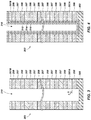
- FIG. 1 is a perspective view of a portion of a memory device including a memory block over a substrate according to an embodiment of this disclosure.
- FIG. 2 is a cross-sectional side view of a vertical string of memory cells of a memory device according to an embodiment of this disclosure, taken at section line A-A of FIG. 1 .
- FIGS. 3-14 are cross-sectional side views illustrating a method of forming a memory device including vertical strings of memory cells, at various stages of the method, according to an embodiment of this disclosure.
- FIG. 15 shows a schematic block diagram of an electronic system according to an embodiment of the present disclosure
- the term “substantially” in reference to a given parameter, property, or condition means and includes to a degree that one skilled in the art would understand that the given parameter, property, or condition is met with a small degree of variance, such as within acceptable manufacturing tolerances.
- a parameter that is substantially met may be at least about 90% met, at least about 95% met, or even at least about 99% met.
- any relational term such as “first,” “second,” “over,” “top,” “bottom,” “underlying,” etc., is used for clarity and convenience in understanding the disclosure and accompanying drawings and does not connote or depend on any specific preference, orientation, or order, except where the context clearly indicates otherwise.
- vertical and horizontal merely refer to a drawing figure as oriented on the drawing sheet, and in no way are limiting of orientation of a device or any portion thereof.
- the terms “forming” and “formed” mean and include any method of creating, building, depositing, and/or patterning a material.
- forming may be accomplished by atomic layer deposition (ALD), chemical vapor deposition (CVD), physical vapor deposition (PVD), sputtering, co-sputtering, spin-coating, diffusing, depositing, growing, or any other technique known in the art of semiconductor fabrication.
- Material may be formed and/or patterned into various shapes and configurations using known techniques, such as isotropic etching, anisotropic etching, chemical-mechanical polishing (CMP), ablating, etc.
- the technique for forming the material may be selected by a person of ordinary skill in the art.
- the term “substrate” means and includes a base material or construction upon which additional materials are formed.
- the substrate may be a semiconductor substrate, a base semiconductor layer on a supporting structure, a metal electrode, or a semiconductor substrate having one or more layers, structures or regions formed thereon.
- the substrate may be a conventional silicon substrate or other bulk substrate comprising a layer of semiconductive material.
- the term “bulk substrate” means and includes not only silicon wafers, but also silicon-on-insulator (SOI) substrates, such as silicon-on-sapphire (SOS) substrates and silicon-on-glass (SOG) substrates, epitaxial layers of silicon on a base semiconductor foundation, and other semiconductor or optoelectronic materials, such as silicon-germanium, germanium, gallium arsenide, gallium nitride, and indium phosphide.
- SOI silicon-on-insulator
- SOS silicon-on-sapphire
- SOOG silicon-on-glass
- epitaxial layers of silicon on a base semiconductor foundation and other semiconductor or optoelectronic materials, such as silicon-germanium, germanium, gallium arsenide, gallium nitride, and indium phosphide.
- the substrate may be doped or undoped.
- a substrate may comprise at least one of silicon, silicon dioxide, silicon with native oxide, silicon nitride, a carbon-containing silicon nitride, glass, semiconductor, metal oxide, metal, titanium nitride, carbon-containing titanium nitride, tantalum, tantalum nitride, carbon-containing tantalum nitride, niobium, niobium nitride, carbon-containing niobium nitride, molybdenum, molybdenum nitride, carbon-containing molybdenum nitride, tungsten, tungsten nitride, carbon-containing tungsten nitride, copper, cobalt, nickel, iron, aluminum, and a noble metal.
- memory devices and electronic systems of this disclosure may include an array of vertical memory cells positioned along respective vertical channels to define vertical memory strings.
- Each of the vertical channels may include a channel material exhibiting an electron mobility of at least about 30 cm 2 /(V ⁇ s) and a room temperature band gap of at least about 1.40 eV (e.g., zinc oxide, silicon carbide, indium phosphide, indium gallium zinc oxide, or gallium arsenide, as well as so-called “2D materials,” such as molybdenum disulfide), and a bottom plug material exhibiting a room temperature band gap of less than about 1.10 eV (e.g., silicon germanium, germanium, or indium gallium arsenide).
- a channel material exhibiting an electron mobility of at least about 30 cm 2 /(V ⁇ s) and a room temperature band gap of at least about 1.40 eV (e.g., zinc oxide, silicon carbide, indium phosphide, indium gallium zinc oxide, or gallium ar
- Such channel materials may allow for an increase in string current as compared to certain conventional vertical memory strings with channel materials having lower electron mobility and lower band gaps.
- Such bottom plug materials may result in an increased GIDL current to facilitate erase operations of the respective vertical memory strings compared to certain conventional vertical memory strings with bottom plugs having higher band gaps.
- FIG. 1 illustrates a portion of a memory device 100 according to an embodiment of the present disclosure that includes a substrate 102 and a stack 104 of alternating conductive gate materials 106 and dielectric materials 108 over the substrate 102 .
- Vertical channels 110 may be arranged in an array and extend through the stack 104 of conductive gate materials 106 and dielectric materials 108 .
- peripheral portions, connections e.g., a so-called “stair-step structure”
- contacts e.g., bit lines
- surrounding insulating material e.g., surrounding insulating material
- FIG. 2 illustrates a cross-sectional side view of the memory device 100 through one of the vertical channels 110 of the stack 104 and the underlying substrate 102 .
- An outer oxide liner 112 may be positioned along a sidewall of and within the vertical channel 110 , in contact with the stack 104 of alternating conductive gate materials 106 and dielectric materials 108 .
- a nitride liner 114 may be positioned adjacent to, inside, and in contact with the outer oxide liner 112 .
- An inner oxide liner 116 may be positioned adjacent to, inside, and in contact with the nitride liner 114 .
- a channel material 118 may be positioned adjacent to, inside, and in contact with the inner oxide liner 116 .
- An individual conductive gate material 106 and an adjacent portion of the outer oxide liner 112 , nitride liner 114 , inner oxide liner 116 , and channel material 118 may define a vertical memory cell 120 of a so-called metal-oxide-nitride-oxide-semiconductor (“MONOS”) configuration.
- MONOS metal-oxide-nitride-oxide-semiconductor
- a bottom plug material 122 may be located between the substrate 102 and the channel material 118 of the vertical channel 110 .
- the bottom plug material 122 may extend upward from the substrate 102 to at least partially vertically overlap a lowermost conductive gate material 106 A.
- the lowermost conductive gate material 106 A may have a vertical thickness T L that is greater than respective thicknesses of the other conductive gate materials 106 of the stack 104 , to provide a larger margin of error when forming the bottom plug material 122 to at least partially vertically overlap the lowermost conductive gate material 106 A.
- the vertical thickness T L of the lowermost conductive gate material 106 A may be about 45 nm or greater, while the respective vertical thicknesses of the other conductive gate materials 106 may be about 35 nm.
- a top plug material 124 may be located between the channel material 118 and a data line 126 (e.g., a bit line).
- the top plug material 124 may at least partially vertically overlap an uppermost conductive gate material 106 B.
- One or more (e.g., from one to five) of the lowermost conductive gate materials 106 , 106 A may be configured as select gate sources.
- One or more (e.g., from one to five) of the uppermost conductive gate materials 106 , 106 B may be configured as select gate drains.
- the conductive gate materials 106 between the select gate source(s) and the select gate drain(s) may be configured as access lines (e.g., word lines). There may be any suitable number of access lines in the stack 104 , such as about 32, about 64, about 72, about 96, or about 128, for example.
- a cap dielectric material 128 which may include one or more different dielectric materials, may be positioned over the stack 104 of alternating conductive gate materials 106 and dielectric materials 108 , adjacent to the data line 126 (e.g., the data line 126 may extend horizontally through the cap dielectric material 128 ).
- the channel material 118 may be in the form of a liner having a sidewall thickness T C of less than about 25 nm, such as between about 5 nm and about 20 nm.
- the channel material 118 may be present along internal sidewalls of the inner oxide liner 116 and over a top surface of the bottom plug material 122 , as illustrated in FIG. 2 .
- a central dielectric 130 may be positioned adjacent to and within sidewalls of the channel material 118 .
- the central dielectric 130 may be or include, for example, an oxide material or an air-filled void.
- the channel material 118 may be, or include, a material that exhibits an electron mobility of at least about 30 cm 2 /(V ⁇ s), such as between about 40 cm 2 /(V ⁇ s) and about 50 cm 2 /(V ⁇ s), and a room temperature band gap of at least about 1.40 eV, such as about 3.3 eV.
- the channel material 118 may be or include zinc oxide, silicon carbide, indium phosphide, indium gallium zinc oxide, or gallium arsenide, as well as so-called “2D materials,” such as molybdenum disulfide.
- the channel material 118 may include stoichiometric variations of the listed materials, and/or combinations of materials such as indium and gallium.
- the channel material 118 may have different composition ratios.
- zinc oxide exhibits an electron mobility of about 40 cm 2 /(V ⁇ s) and a room temperature band gap of about 3.3 eV.
- Zinc oxide also has an electron affinity of about 4.29 eV, which is close to polysilicon's electron affinity of about 4.1 eV.
- the bottom plug material 122 may be, or include, a material that exhibits a room temperature band gap of less than about 1.10 eV.
- the bottom plug material 122 may be or include silicon germanium (which has a room temperature band bap of about 0.85 eV), germanium (which has a room temperature band gap of about 0.66 eV), or indium gallium arsenide (which has a room temperature band gap of about 0.7 eV).
- the bottom plug material 122 may be doped with an n-type dopant.
- embodiments of this disclosure include memory devices that include an array of vertical memory cells positioned along respective vertical channels to define vertical memory strings.
- Each of the vertical channels includes a channel material and a bottom plug material at a base of the vertical channel and electrically coupled to the channel material.
- the channel material exhibits an electron mobility of at least about 30 cm 2 /(V ⁇ s) and a room temperature band gap of at least about 1.40 eV.
- the bottom plug material exhibits a room temperature band gap of less than about 1.10 eV
- FIGS. 3-14 illustrate a method of forming a memory device including vertical strings of memory cells, at various stages of the method, according to an embodiment of this disclosure. For simplicity, the formation of a single vertical string of memory cells is illustrated, but will be understood by one of ordinary skill in the art that the method may include simultaneously forming multiple (e.g., an array of) vertical strings of memory cells.
- a stack 203 of alternating first dielectric materials 207 and second dielectric materials 208 may be formed over a substrate 202 , and vertical channels 210 may be formed through the stack 203 to expose the substrate 202 .
- the substrate 202 may be, or include, a semiconductor material, such as silicon (e.g., polysilicon) or silicon germanium, for example.
- the first dielectric materials 207 and second dielectric materials 208 may be formed over the substrate 202 in alternating fashion.
- the stack 203 may be formed with any number of respective first dielectric materials 207 and second dielectric materials 208 , such as about 32, about 64, about 96, or about 128, for example.
- the formation of the first and second dielectric materials 207 , 208 may be accomplished by, for example, chemical vapor deposition (CVD), atomic layer deposition (ALD), a spin-on process, etc.
- the first and second dielectric materials 207 , 208 may be different from, and may exhibit etch selectivity with respect to, each other.
- the first dielectric materials 207 may be or include silicon nitride and the second dielectric materials 208 may be or include silicon oxide.
- a lowermost first dielectric material 207 A may be formed to have a greater vertical thickness T L (e.g., about 45 nm) than each the remaining first dielectric materials 207 in the stack 203 (which may have a vertical thickness of, e.g., about 35 nm).
- An uppermost first dielectric material 207 B may serve as a sacrificial protective barrier for the stack 203 during subsequent processing steps.
- the first dielectric materials 207 or portions thereof may later be removed and replaced by conductive gate materials 206 .
- the stack 203 may be initially formed to include the alternating conductive gate materials 206 in place of the first dielectric materials 207 .
- portions of the stack 203 may be removed to form the vertical channels 210 through the stack 203 to expose the substrate 202 at a base of the vertical channels 210 .
- the portions of the stack 203 may be removed by an anisotropic photolithographic process, including formation of a mask material (not shown) over the stack 203 , photolithographically patterning and developing the mask material to remove material and form openings over the intended locations of the vertical channels 210 , and removing (e.g., etching) the portions of the first and second dielectric materials 207 , 208 directly beneath the openings in the mask.
- an outer oxide liner 212 , nitride liner 214 , and inner oxide liner 216 may be formed within and along internal sidewalls of the vertical channel 210 , as well as over a top surface of the stack 203 and over the exposed portion of the substrate 202 at the base of the vertical channel 210 .
- the outer oxide liner 212 , nitride liner 214 , and inner oxide liner 216 may be formed by a conformal deposition process, such as ALD.
- portions of the outer oxide liner 212 , nitride liner 214 , and inner oxide liner 216 that are formed over horizontal surfaces, such as over the top surface of the stack 203 and over the exposed surface of the substrate 202 at the base of the vertical channel 210 , may be removed.
- the removal may be accomplished by, for example, forming a polysilicon liner (not shown) over the inner oxide liner 216 , removing portions of the polysilicon liner over the horizontal surfaces, and performing an anisotropic etching process to expose portions of the inner oxide liner 216 over the horizontal surfaces.
- the polysilicon liner may remain over vertical surfaces of the inner oxide liner 216 to protect the inner oxide liner 216 from a subsequent material removal process.
- Portions of the inner oxide liner 216 , nitride liner 214 , and outer oxide liner 214 exposed through the polysilicon liner may be removed by a chemical etching process. The polysilicon liner may then be removed. Portions of the outer oxide liner 212 , nitride liner 214 , and inner oxide liner 216 that are formed over vertical surfaces, such as over the internal sidewalls of the vertical channel 210 , may remain after the removal process, as shown in FIG. 5 .
- a bottom plug material 222 may be formed within and at a base of the vertical channel 210 .
- the bottom plug material 222 may be a semiconductor material exhibiting a room temperature band gap of less than about 1.10 eV.
- the bottom plug material 222 may be or include silicon germanium, germanium, or indium gallium arsenide.
- the bottom plug material 222 may include an n-type dopant. Forming the bottom plug material 222 from a material that exhibits a band gap of less than about 1.10 eV may increase a GIDL current in string erase operations of a resulting device, compared to bottom plug materials exhibiting a higher band gap.
- the bottom plug material 222 may be epitaxially grown, using the substrate 202 (e.g., polysilicon) as a seed material.
- the bottom plug material 222 may be formed to at least partially overlap the lowermost first dielectric material 207 A.
- an upper extent of the bottom plug material 222 may be about one-half to about two-thirds up the vertical thickness of the lowermost first dielectric material 207 A.
- Previously forming the lowermost first dielectric material 207 A to have a greater thickness T L ( FIG. 3 ) than the remaining first dielectric materials 207 allows for a wider margin of error when forming the bottom plug material 222 to have an upper extent in an intended location relative to the lowermost first dielectric material 207 A.
- a channel material 218 may be formed within the vertical channel 210 .
- the channel material 218 may be formed as a conformal film along the inner sidewalls of the vertical channel 210 , over the bottom plug material 222 , and over a top surface of the stack 203 .
- the channel material 218 may have a thickness T C of less than about 25 nm, for example, such as between about 5 nm and about 20 nm. Forming the channel material 218 as a conformal film may result in better electrical performance of a resulting memory device, compared to forming the channel material 218 to substantially fill the vertical channel 210 . Nonetheless, in other embodiments, the channel material 218 may be formed to substantially fill the vertical channel 210 , such as to reduce manufacturing costs.
- the channel material 218 may be a semiconductor material exhibiting an electron mobility of at least about 30 cm 2 /(V ⁇ s) and a room temperature band gap of at least about 1.40 eV.
- the channel material 218 may be or include zinc oxide, silicon carbide, indium phosphide, indium gallium zinc oxide, or gallium arsenide, as well as so-called “2D materials,” such as molybdenum disulfide.
- the channel material 218 may include stoichiometric variations of the listed materials, and/or combinations of materials such as indium and gallium.
- the channel material 218 may have different composition ratios.
- the channel material 218 may be formed using a conformal deposition process, such as ALD.
- the channel material 218 may be undoped, or may include a p-type dopant or an n-type dopant.
- a central dielectric 230 may be formed to substantially fill the vertical channel 210 adjacent to the channel material 218 .
- an air-filled void may be left within the vertical channel 210 adjacent to the channel material 218 .
- the central dielectric 230 may be any dielectric material, such as an oxide material (e.g., silicon oxide).
- the central dielectric may be formed of a so-called “spin-on dielectric” or “SOD” material by depositing a flowable dielectric over the stack 203 and spinning the substrate 202 to spread the flowable dielectric across upper surfaces of the stack 203 and into the vertical channels 210 .
- the flowable dielectric may then be densified, such as by heat or chemical treating.
- portions of the central dielectric 230 over a top surface of the stack 203 may be removed, such as by a chemical-mechanical planarization (CMP) process.
- CMP chemical-mechanical planarization
- a portion of the remaining central dielectric 230 proximate a top of the vertical channel 210 may be removed, to recess a top surface of the central dielectric 230 below the top surface of the stack 203 .
- the central dielectric 230 may be recessed by an etch process, such as by exposing the central dielectric to an etchant configured to remove the material of the central dielectric 230 but that does not remove the material of the channel material 218 .
- the central dielectric 230 may be recessed to a vertical level such that a space above the central dielectric 230 at least partially overlaps with what will become an uppermost select gate drain (e.g., an upper first dielectric material 207 that will be replaced by a conductive gate material 206 ( FIG. 13 ) configured for functioning as an uppermost select gate drain).
- an uppermost select gate drain e.g., an upper first dielectric material 207 that will be replaced by a conductive gate material 206 ( FIG. 13 ) configured for functioning as an uppermost select gate drain.
- portions of the channel material 218 over a top surface of the stack 203 and within the vertical channel 210 above the recessed central dielectric 230 may be removed, such as using an etch configured to remove the channel material 218 but not remove the first or second dielectric materials 207 , 208 , outer oxide liner 212 , nitride liner 214 , inner oxide liner 216 , or central dielectric 230 .
- the portions of the channel material 218 may be removed by exposure to a solution of hydrofluoric acid and water, hydrochloric acid and water, or phosphoric acid and water.
- a top plug material 224 may be formed within the vertical channel 210 and electrically coupled to the channel material 218 .
- the top plug material 224 may be a semiconductor material, such as polysilicon, silicon germanium, or germanium, for example.
- the top plug material 224 may include an n-type dopant.
- the process for forming the top plug material 224 may be, for example, CVD.
- the top plug material 224 may initially be formed over a top surface of the stack 203 , in addition to within the vertical channel 210 .
- portions of the top plug material 224 over a top surface of the stack 203 may be removed, such as by CMP or etching.
- the uppermost first dielectric material 207 B which previously served as a sacrificial barrier layer during prior processing acts, may be removed, such as by CMP or etching.
- a cap dielectric material 228 may be formed over the stack 203 .
- the cap dielectric material 228 may include one or more dielectric materials, such as silicon oxide and/or silicon nitride.
- the first dielectric materials 207 may be removed and replaced by conductive gate materials 206 .
- one or more openings may be formed through the stack 203 to expose each of the first dielectric materials 207 in the stack 203 .
- An isotropic material removal process may be performed to selectively remove the first dielectric materials 207 , without removing the second dielectric material 208 .
- an etchant may be introduced into the one or more openings and in contact with the first dielectric materials 207 to remove the first dielectric materials 207 and to form gaps between the second dielectric materials 208 .
- the conductive gate materials 206 may be formed by introducing a conductive material (e.g., one or more of titanium, titanium nitride, tantalum, tantalum nitride, tungsten, or tungsten nitride) into the one or more openings and into the gaps left by removal of the first dielectric materials 207 , such as by a deposition process (e.g., CVD or ALD). Any residual conductive material within the openings may be removed, and the openings may be filled with a dielectric material.
- a conductive material e.g., one or more of titanium, titanium nitride, tantalum, tantalum nitride, tungsten, or tungsten nitride
- the process of forming the conductive gate materials 206 described above, including forming the outer oxide liner 212 , nitride liner 214 , inner oxide liner 216 , and channel material 218 prior to replacing the first dielectric materials 207 with the conductive gate materials 206 introduced through openings, may be referred to as a so-called “replacement gate” process.
- this disclosure is not limited to forming the conductive gate materials 206 using such a replacement gate process.
- this disclosure is also applicable to a so-called “floating gate” process, in which portions of first dielectric materials 207 are replaced with conductive gate materials 206 introduced through the vertical channels 210 prior to forming the outer oxide liner 212 , nitride liner 214 , inner oxide liner 216 , and channel material 218 .
- an individual conductive gate material 206 and an adjacent portion of the outer oxide liner 212 , nitride liner 214 , inner oxide liner 216 , and channel material 218 may define an individual memory cell 220 .
- the group of memory cells 220 located along a particular vertical channel 210 may define a vertical string of memory cells 220 .
- a data line 226 (e.g., bit line) may be formed over and electrically coupled to the top plug material 224 for providing electrical access to the vertical string of memory cells 220 .
- portions of the cap dielectric material 228 may be removed (e.g., via photolithography) to define trenches (not shown) within the cap dielectric material 228 , exposing the top plug material 224 .
- a conductive material such as tungsten, tungsten nitride, titanium, titanium nitride, tan may be deposited into the trenches, such as using CVD, to form data lines 226 . Any residual conductive material over a top surface of the cap dielectric material 228 may be removed, such as by CMP.
- the data lines 226 may extend horizontally into and out of the page from the perspective shown in FIG. 14 .
- embodiments of this disclosure include methods of forming memory devices.
- a stack of alternating conductive gate materials and dielectric materials is formed.
- Vertical channels are formed to extend through the stack.
- a bottom plug material, channel material, and top plug material are formed within the vertical channels.
- the bottom plug material exhibits a room temperature band gap of less than about 1.10 eV.
- the channel material exhibits an electron mobility of at least about 30 cm 2 /(V ⁇ s) and a room temperature band gap of at least about 1.40 eV.
- the channel materials and bottom plug materials disclosed herein may provide enhanced current transmission in 3D memory arrays, which may be suitable for use with devices having an increased number of stacked transistors.
- the increased band gap of the disclosed channel materials may reduce boosting leakage compared to certain conventional channel materials, such as polysilicon.
- the channel materials and bottom plug materials may be applicable to all 3D memory architectures including select gate source and select gate drain transistors.
- the channel materials and bottom plug materials may also result in fewer defects and traps than certain conventional channel materials.
- the bottom plug materials disclosed herein may result in increased GIDL current values for improved string erase operations.
- FIG. 15 is a schematic block diagram of an electronic system 300 according to an embodiment of the present disclosure.
- the electronic system 300 includes a processor 310 electrically coupled with a memory device 320 , one or more input devices 330 , and one or more output devices 340 .
- the electronic system 300 may be a consumer electronic device, such as a desktop computer, a laptop computer, a tablet computer, an electronic reader, a smart phone, or other type of communication device, as well as any type of computing system incorporating a memory device.
- the memory device 320 may be or include a memory device (e.g., one or more of the memory devices 100 , 200 ) that includes a channel material exhibiting an electron mobility of at least about 30 cm 2 /(V ⁇ s) and a room temperature band gap of at least about 1.40 eV (e.g., ZnO, IGZO, SiC, InP, GaAs, MoS 2 ), as well as a bottom plug material exhibiting a room temperature band gap of less than about 1.10 eV (e.g., silicon germanium, germanium, or indium gallium arsenide), as discussed above.
- a memory device e.g., one or more of the memory devices 100 , 200
- a channel material exhibiting an electron mobility of at least about 30 cm 2 /(V ⁇ s) and a room temperature band gap of at least about 1.40 eV (e.g., ZnO, IGZO, SiC, InP, GaAs, MoS 2 ), as well as a
- embodiments of this disclosure include electronic systems including a processor and a memory device electrically coupled to the processor.
- the memory device includes an array of vertical memory cells positioned along respective vertical channels to define vertical memory strings.
- Each of the vertical channels includes a channel material selected from the group consisting of zinc oxide, silicon carbide, indium phosphide, indium gallium zinc oxide, gallium arsenide, and molybdenum disulfide, and a bottom plug material electrically coupled to a base of the channel material, the bottom plug material selected from the group consisting of silicon germanium, germanium, and indium gallium arsenide.
Landscapes
- Engineering & Computer Science (AREA)
- Physics & Mathematics (AREA)
- Condensed Matter Physics & Semiconductors (AREA)
- General Physics & Mathematics (AREA)
- Manufacturing & Machinery (AREA)
- Computer Hardware Design (AREA)
- Microelectronics & Electronic Packaging (AREA)
- Power Engineering (AREA)
- Chemical & Material Sciences (AREA)
- Crystallography & Structural Chemistry (AREA)
- Semiconductor Memories (AREA)
Abstract
Description
Claims (22)
Priority Applications (3)
| Application Number | Priority Date | Filing Date | Title |
|---|---|---|---|
| US16/111,357 US10608012B2 (en) | 2017-08-29 | 2018-08-24 | Memory devices including memory cells and related methods |
| US16/822,696 US11107832B2 (en) | 2017-08-29 | 2020-03-18 | Apparatuses including memory cells and related methods |
| US17/445,157 US20210375925A1 (en) | 2017-08-29 | 2021-08-16 | Apparatuses including memory cells and related methods |
Applications Claiming Priority (2)
| Application Number | Priority Date | Filing Date | Title |
|---|---|---|---|
| US201762551347P | 2017-08-29 | 2017-08-29 | |
| US16/111,357 US10608012B2 (en) | 2017-08-29 | 2018-08-24 | Memory devices including memory cells and related methods |
Related Child Applications (1)
| Application Number | Title | Priority Date | Filing Date |
|---|---|---|---|
| US16/822,696 Continuation US11107832B2 (en) | 2017-08-29 | 2020-03-18 | Apparatuses including memory cells and related methods |
Publications (2)
| Publication Number | Publication Date |
|---|---|
| US20190067326A1 US20190067326A1 (en) | 2019-02-28 |
| US10608012B2 true US10608012B2 (en) | 2020-03-31 |
Family
ID=65435633
Family Applications (3)
| Application Number | Title | Priority Date | Filing Date |
|---|---|---|---|
| US16/111,357 Active US10608012B2 (en) | 2017-08-29 | 2018-08-24 | Memory devices including memory cells and related methods |
| US16/822,696 Active US11107832B2 (en) | 2017-08-29 | 2020-03-18 | Apparatuses including memory cells and related methods |
| US17/445,157 Pending US20210375925A1 (en) | 2017-08-29 | 2021-08-16 | Apparatuses including memory cells and related methods |
Family Applications After (2)
| Application Number | Title | Priority Date | Filing Date |
|---|---|---|---|
| US16/822,696 Active US11107832B2 (en) | 2017-08-29 | 2020-03-18 | Apparatuses including memory cells and related methods |
| US17/445,157 Pending US20210375925A1 (en) | 2017-08-29 | 2021-08-16 | Apparatuses including memory cells and related methods |
Country Status (1)
| Country | Link |
|---|---|
| US (3) | US10608012B2 (en) |
Cited By (4)
| Publication number | Priority date | Publication date | Assignee | Title |
|---|---|---|---|---|
| US10892366B2 (en) * | 2018-06-25 | 2021-01-12 | Samsung Electronics Co., Ltd. | Thin film transistor and vertical non-volatile memory device including transition metal-induced polycrystalline metal oxide channel layer |
| US11948992B2 (en) | 2021-01-26 | 2024-04-02 | Micron Technology, Inc . | Electronic devices comprising a dielectric material, and related systems and methods |
| US11974430B2 (en) | 2021-01-26 | 2024-04-30 | Micron Technology, Inc. | Microelectronic devices with dopant extensions near a GIDL region below a tier stack, and related methods and systems |
| US12356617B2 (en) | 2021-01-26 | 2025-07-08 | Micron Technology, Inc. | Microelectronic devices with vertically recessed channel structures and discrete, spaced inter-slit structures, and related methods and systems |
Families Citing this family (14)
| Publication number | Priority date | Publication date | Assignee | Title |
|---|---|---|---|---|
| EP3811406B1 (en) * | 2018-09-27 | 2024-05-01 | Yangtze Memory Technologies Co., Ltd. | Semiconductor plug protected by protective dielectric layer in three-dimensional memory device and method for forming the same |
| JP2020072191A (en) * | 2018-10-31 | 2020-05-07 | キオクシア株式会社 | Semiconductor memory device |
| KR102179934B1 (en) * | 2019-06-04 | 2020-11-17 | 서울대학교산학협력단 | 3 dimensional resistive switching memory device and method of fabricating the same |
| US11594644B2 (en) * | 2019-11-13 | 2023-02-28 | Micron Technology, Inc. | Microelectronic devices including passivation materials, related electronic devices, and related methods |
| US11404583B2 (en) * | 2019-12-31 | 2022-08-02 | Micron Technology, Inc. | Apparatus including multiple channel materials, and related methods, memory devices, and electronic systems |
| CN111466026B (en) * | 2020-03-11 | 2022-06-07 | 长江存储科技有限责任公司 | Three-dimensional memory device with two-dimensional material |
| US11889683B2 (en) * | 2020-07-01 | 2024-01-30 | Micron Technology, Inc. | Memory arrays comprising strings of memory cells and methods used in forming a memory array comprising strings of memory cells |
| WO2022149721A1 (en) * | 2021-01-11 | 2022-07-14 | 한양대학교 산학협력단 | Three-dimensional flash memory including channel layer having multilayer structure, and method for manufacturing same |
| KR102666996B1 (en) * | 2021-03-26 | 2024-05-17 | 한양대학교 산학협력단 | 3 demensional flash memory including channel layer of multilayer structure and manufacturing method thereof |
| KR102578436B1 (en) * | 2021-01-12 | 2023-09-14 | 한양대학교 산학협력단 | 3 dimensional flash memory for improving contact resistance of igzo channel |
| US11935930B2 (en) * | 2021-11-30 | 2024-03-19 | International Business Machines Corporation | Wrap-around-contact for 2D-channel gate-all-around field-effect-transistors |
| US12382662B2 (en) | 2021-11-30 | 2025-08-05 | International Business Machines Corporation | Wrap-around-contact for 2D-channel gate-all-around field-effect-transistors |
| KR20230135919A (en) * | 2022-03-17 | 2023-09-26 | 삼성전자주식회사 | Semiconductor device including vertical channel structure |
| KR102875603B1 (en) * | 2023-12-13 | 2025-10-24 | 한양대학교 산학협력단 | 3d flash memory with silicon-based channel structure |
Citations (15)
| Publication number | Priority date | Publication date | Assignee | Title |
|---|---|---|---|---|
| US20100213458A1 (en) | 2009-02-23 | 2010-08-26 | Micron Technology, Inc. | Rigid semiconductor memory having amorphous metal oxide semiconductor channels |
| US8513073B1 (en) | 2012-08-27 | 2013-08-20 | International Business Machines Corporation | Silicon germanium channel with silicon buffer regions for fin field effect transistor device |
| US8530350B2 (en) | 2011-06-02 | 2013-09-10 | Micron Technology, Inc. | Apparatuses including stair-step structures and methods of forming the same |
| US8766320B2 (en) | 2011-02-03 | 2014-07-01 | Micron Technology, Inc. | Memory devices with a connecting region having a band gap lower than a band gap of a body region |
| US20140264525A1 (en) | 2013-03-12 | 2014-09-18 | SanDisk Technologies, Inc. | Vertical nand and method of making thereof using sequential stack etching and landing pad |
| US20150137114A1 (en) * | 2011-08-31 | 2015-05-21 | Snu R&Db Foundation | Electronic device and method for manufacturing same |
| US9177872B2 (en) | 2011-09-16 | 2015-11-03 | Micron Technology, Inc. | Memory cells, semiconductor devices, systems including such cells, and methods of fabrication |
| US9209199B2 (en) | 2014-03-21 | 2015-12-08 | Intel Corporation | Stacked thin channels for boost and leakage improvement |
| US9240420B2 (en) | 2013-09-06 | 2016-01-19 | Sandisk Technologies Inc. | 3D non-volatile storage with wide band gap transistor decoder |
| US9281318B2 (en) | 2013-03-06 | 2016-03-08 | Intel Corporation | Three dimensional memory structure |
| US20160104719A1 (en) * | 2014-10-14 | 2016-04-14 | Won-Seok Jung | Semiconductor Memory Devices and Methods of Fabricating the Same |
| US20160149004A1 (en) * | 2014-11-25 | 2016-05-26 | Sandisk Technologies Inc. | 3D NAND With Oxide Semiconductor Channel |
| US9437604B2 (en) | 2013-11-01 | 2016-09-06 | Micron Technology, Inc. | Methods and apparatuses having strings of memory cells including a metal source |
| US9536618B2 (en) | 2012-12-06 | 2017-01-03 | Micron Technology, Inc. | Apparatuses and methods to control body potential in memory operations |
| US20170053986A1 (en) | 2015-08-17 | 2017-02-23 | Micron Technology, Inc. | Integrated Structures Containing Vertically-Stacked Memory Cells |
Family Cites Families (11)
| Publication number | Priority date | Publication date | Assignee | Title |
|---|---|---|---|---|
| JP2794678B2 (en) * | 1991-08-26 | 1998-09-10 | 株式会社 半導体エネルギー研究所 | Insulated gate semiconductor device and method of manufacturing the same |
| TW324101B (en) * | 1995-12-21 | 1998-01-01 | Hitachi Ltd | Semiconductor integrated circuit and its working method |
| JP2002050764A (en) * | 2000-08-02 | 2002-02-15 | Matsushita Electric Ind Co Ltd | Thin film transistor, array substrate, liquid crystal display device, organic EL display device and method of manufacturing the same |
| AU2002348933A1 (en) * | 2001-11-21 | 2003-06-10 | Koninklijke Philips Electronics N.V. | Heterojunction semiconductor device and method of manufacturing such device |
| KR100637101B1 (en) * | 2005-04-21 | 2006-10-20 | 주식회사 하이닉스반도체 | Semiconductor device including a contact plug having a double structure of epitaxial stack and metal layer, and manufacturing method thereof |
| KR101482639B1 (en) * | 2009-03-06 | 2015-01-22 | 삼성전자주식회사 | Nonvolatile memory element |
| KR20130045622A (en) * | 2011-10-26 | 2013-05-06 | 에스케이하이닉스 주식회사 | 3d structured non-volatile memory device ane method for manufacturing the same |
| US8853069B2 (en) * | 2012-09-10 | 2014-10-07 | Globalfoundries Inc. | Field effect transistor and method of fabrication |
| KR20160060850A (en) * | 2014-11-20 | 2016-05-31 | 삼성전자주식회사 | Memory device and manufactureing the same |
| KR102384893B1 (en) * | 2015-05-21 | 2022-04-08 | 삼성전자주식회사 | Semiconductor devices and methods of manufacturing the same |
| TWI580058B (en) * | 2016-10-26 | 2017-04-21 | 財團法人工業技術研究院 | Solar battery |
-
2018
- 2018-08-24 US US16/111,357 patent/US10608012B2/en active Active
-
2020
- 2020-03-18 US US16/822,696 patent/US11107832B2/en active Active
-
2021
- 2021-08-16 US US17/445,157 patent/US20210375925A1/en active Pending
Patent Citations (16)
| Publication number | Priority date | Publication date | Assignee | Title |
|---|---|---|---|---|
| US20100213458A1 (en) | 2009-02-23 | 2010-08-26 | Micron Technology, Inc. | Rigid semiconductor memory having amorphous metal oxide semiconductor channels |
| US8766320B2 (en) | 2011-02-03 | 2014-07-01 | Micron Technology, Inc. | Memory devices with a connecting region having a band gap lower than a band gap of a body region |
| US8530350B2 (en) | 2011-06-02 | 2013-09-10 | Micron Technology, Inc. | Apparatuses including stair-step structures and methods of forming the same |
| US20150137114A1 (en) * | 2011-08-31 | 2015-05-21 | Snu R&Db Foundation | Electronic device and method for manufacturing same |
| US9177872B2 (en) | 2011-09-16 | 2015-11-03 | Micron Technology, Inc. | Memory cells, semiconductor devices, systems including such cells, and methods of fabrication |
| US8513073B1 (en) | 2012-08-27 | 2013-08-20 | International Business Machines Corporation | Silicon germanium channel with silicon buffer regions for fin field effect transistor device |
| US9536618B2 (en) | 2012-12-06 | 2017-01-03 | Micron Technology, Inc. | Apparatuses and methods to control body potential in memory operations |
| US9281318B2 (en) | 2013-03-06 | 2016-03-08 | Intel Corporation | Three dimensional memory structure |
| US20140264525A1 (en) | 2013-03-12 | 2014-09-18 | SanDisk Technologies, Inc. | Vertical nand and method of making thereof using sequential stack etching and landing pad |
| US9240420B2 (en) | 2013-09-06 | 2016-01-19 | Sandisk Technologies Inc. | 3D non-volatile storage with wide band gap transistor decoder |
| US9437604B2 (en) | 2013-11-01 | 2016-09-06 | Micron Technology, Inc. | Methods and apparatuses having strings of memory cells including a metal source |
| US9412821B2 (en) | 2014-03-21 | 2016-08-09 | Intel Corporation | Stacked thin channels for boost and leakage improvement |
| US9209199B2 (en) | 2014-03-21 | 2015-12-08 | Intel Corporation | Stacked thin channels for boost and leakage improvement |
| US20160104719A1 (en) * | 2014-10-14 | 2016-04-14 | Won-Seok Jung | Semiconductor Memory Devices and Methods of Fabricating the Same |
| US20160149004A1 (en) * | 2014-11-25 | 2016-05-26 | Sandisk Technologies Inc. | 3D NAND With Oxide Semiconductor Channel |
| US20170053986A1 (en) | 2015-08-17 | 2017-02-23 | Micron Technology, Inc. | Integrated Structures Containing Vertically-Stacked Memory Cells |
Non-Patent Citations (7)
| Title |
|---|
| Bayraktaroglu et al., Microwave ZnO Thin-Film Transistors, IEEE Electron Device Letters, vol. 29, No. 9, Sep. 2008, pp. 1024-1026. |
| Date et al., Suppression of the Floating-Body Effect Using SiGe Layers in Vertical Surrounding-Gate MOSFETs, IEEE Transactions on Electron Devices, vol. 48, No. 12, Dec. 2001, pp. 2684-2689. |
| Fortunato et al., Wide-Bandgap High-Mobility ZnO Thin-Film Transistors Produced at Room Temperature, Applied Physics Letters, vol. 85, No. 13, Sep. 27, 2004, pp. 2541-2543. |
| Hong et al., High-Performance SiGe Epitaxial Base Bipolar Transistors Produced by a Reduced-Pressure CVD Reactor, IEEE Electron Device Letters, vol. 14, No. 9, Sep. 1993, pp. 450-452. |
| Hwang et al., Vertical Channel ZnO Thin-Film Transistors Using an Atomic Layer Deposition Method, IEEE Electron Device Letters, vol. 35, No. 3, Mar. 2014, pp. 360-362. |
| Pearton et al., Advanced in Processing of ZnO, Elsevier, Zinc Oxide Bulk, Thin Films and Nanostructures, Processing, Properties and Applications, Chapter 9, pp. 314-317. |
| Pillai et al., Transport Mechanism in Sub 1000° C Processed High Mobility Polycrystalline ZnO Transparent Thin Film Transistors, 2015 IEEE International Electron Devices Meeting (IEDM), Dec. 7-9, 2015, 28.1.1-28.1.4. |
Cited By (7)
| Publication number | Priority date | Publication date | Assignee | Title |
|---|---|---|---|---|
| US10892366B2 (en) * | 2018-06-25 | 2021-01-12 | Samsung Electronics Co., Ltd. | Thin film transistor and vertical non-volatile memory device including transition metal-induced polycrystalline metal oxide channel layer |
| US11942553B2 (en) | 2018-06-25 | 2024-03-26 | Samsung Electronics Co., Ltd. | Method for fabricating a semiconductor device |
| US12211940B2 (en) | 2018-06-25 | 2025-01-28 | Samsung Electronics Co., Ltd. | Thin film transistor and vertical non-volatile memory device including transition metal-induced polycrystalline metal oxide channel layer |
| US11948992B2 (en) | 2021-01-26 | 2024-04-02 | Micron Technology, Inc . | Electronic devices comprising a dielectric material, and related systems and methods |
| US11974430B2 (en) | 2021-01-26 | 2024-04-30 | Micron Technology, Inc. | Microelectronic devices with dopant extensions near a GIDL region below a tier stack, and related methods and systems |
| US12356617B2 (en) | 2021-01-26 | 2025-07-08 | Micron Technology, Inc. | Microelectronic devices with vertically recessed channel structures and discrete, spaced inter-slit structures, and related methods and systems |
| US12471283B2 (en) | 2021-01-26 | 2025-11-11 | Micron Technology, Inc. | Microelectronic devices with source region vertical extension between upper and lower channel regions, and related methods |
Also Published As
| Publication number | Publication date |
|---|---|
| US20190067326A1 (en) | 2019-02-28 |
| US20210375925A1 (en) | 2021-12-02 |
| US20200219899A1 (en) | 2020-07-09 |
| US11107832B2 (en) | 2021-08-31 |
Similar Documents
| Publication | Publication Date | Title |
|---|---|---|
| US11107832B2 (en) | Apparatuses including memory cells and related methods | |
| US12029032B2 (en) | Integrated assemblies and methods of forming integrated assemblies | |
| US10115681B1 (en) | Compact three-dimensional memory device having a seal ring and methods of manufacturing the same | |
| US10319680B1 (en) | Metal contact via structure surrounded by an air gap and method of making thereof | |
| CN108475682B (en) | Integration of word line switch and word line contact via structure | |
| US10103169B1 (en) | Method of making a three-dimensional memory device using a multi-step hot phosphoric acid wet etch process | |
| US9530790B1 (en) | Three-dimensional memory device containing CMOS devices over memory stack structures | |
| US9583500B2 (en) | Multilevel memory stack structure and methods of manufacturing the same | |
| US9299716B2 (en) | Methods of manufacturing a semiconductor device | |
| US9711524B2 (en) | Three-dimensional memory device containing plural select gate transistors having different characteristics and method of making thereof | |
| US9524976B2 (en) | Method of integrating select gate source and memory hole for three-dimensional non-volatile memory device | |
| US20200357814A1 (en) | Three-dimensional memory device including signal and power connection lines extending through dielectric regions and methods of making the same | |
| US10256167B1 (en) | Hydrogen diffusion barrier structures for CMOS devices and method of making the same | |
| KR102431682B1 (en) | Semiconductor device structure | |
| EP3646380A1 (en) | Multi-tier three-dimensional memory device with stress compensation structures and method of making thereof | |
| US9812450B2 (en) | Semiconductor devices and methods of manufacturing the same | |
| CN111900164A (en) | Semiconductor structure and preparation method | |
| JP2018509000A (en) | Integration of split-gate flash memory array and logic device | |
| US11316043B2 (en) | Semiconductor transistor device and method of manufacturing the same |
Legal Events
| Date | Code | Title | Description |
|---|---|---|---|
| FEPP | Fee payment procedure |
Free format text: ENTITY STATUS SET TO UNDISCOUNTED (ORIGINAL EVENT CODE: BIG.); ENTITY STATUS OF PATENT OWNER: LARGE ENTITY |
|
| STPP | Information on status: patent application and granting procedure in general |
Free format text: DOCKETED NEW CASE - READY FOR EXAMINATION |
|
| AS | Assignment |
Owner name: JPMORGAN CHASE BANK, N.A.., AS COLLATERAL AGENT, I Free format text: SUPPLEMENT NO. 1 TO PATENT SECURITY AGREEMENT;ASSIGNOR:MICRON TECHNOLOGY, INC.;REEL/FRAME:047630/0756 Effective date: 20181015 Owner name: MORGAN STANLEY SENIOR FUNDING, INC., AS COLLATERAL Free format text: SUPPLEMENT NO. 10 TO PATENT SECURITY AGREEMENT;ASSIGNOR:MICRON TECHNOLOGY, INC.;REEL/FRAME:048102/0420 Effective date: 20181015 Owner name: JPMORGAN CHASE BANK, N.A.., AS COLLATERAL AGENT, ILLINOIS Free format text: SUPPLEMENT NO. 1 TO PATENT SECURITY AGREEMENT;ASSIGNOR:MICRON TECHNOLOGY, INC.;REEL/FRAME:047630/0756 Effective date: 20181015 Owner name: MORGAN STANLEY SENIOR FUNDING, INC., AS COLLATERAL AGENT, MARYLAND Free format text: SUPPLEMENT NO. 10 TO PATENT SECURITY AGREEMENT;ASSIGNOR:MICRON TECHNOLOGY, INC.;REEL/FRAME:048102/0420 Effective date: 20181015 |
|
| STPP | Information on status: patent application and granting procedure in general |
Free format text: NON FINAL ACTION MAILED |
|
| AS | Assignment |
Owner name: MICRON TECHNOLOGY, INC., IDAHO Free format text: ASSIGNMENT OF ASSIGNORS INTEREST;ASSIGNORS:HUANG, GUANGYU;LIU, HAITAO;MOULI, CHANDRA V.;AND OTHERS;SIGNING DATES FROM 20180822 TO 20180823;REEL/FRAME:049751/0424 |
|
| STPP | Information on status: patent application and granting procedure in general |
Free format text: RESPONSE TO NON-FINAL OFFICE ACTION ENTERED AND FORWARDED TO EXAMINER |
|
| AS | Assignment |
Owner name: MICRON TECHNOLOGY, INC., IDAHO Free format text: RELEASE BY SECURED PARTY;ASSIGNOR:MORGAN STANLEY SENIOR FUNDING, INC., AS COLLATERAL AGENT;REEL/FRAME:050719/0550 Effective date: 20190731 |
|
| AS | Assignment |
Owner name: MICRON TECHNOLOGY, INC., IDAHO Free format text: RELEASE BY SECURED PARTY;ASSIGNOR:JPMORGAN CHASE BANK, N.A., AS COLLATERAL AGENT;REEL/FRAME:051028/0835 Effective date: 20190731 |
|
| STPP | Information on status: patent application and granting procedure in general |
Free format text: NOTICE OF ALLOWANCE MAILED -- APPLICATION RECEIVED IN OFFICE OF PUBLICATIONS |
|
| STPP | Information on status: patent application and granting procedure in general |
Free format text: PUBLICATIONS -- ISSUE FEE PAYMENT RECEIVED |
|
| STPP | Information on status: patent application and granting procedure in general |
Free format text: PUBLICATIONS -- ISSUE FEE PAYMENT VERIFIED |
|
| STCF | Information on status: patent grant |
Free format text: PATENTED CASE |
|
| MAFP | Maintenance fee payment |
Free format text: PAYMENT OF MAINTENANCE FEE, 4TH YEAR, LARGE ENTITY (ORIGINAL EVENT CODE: M1551); ENTITY STATUS OF PATENT OWNER: LARGE ENTITY Year of fee payment: 4 |