US10607902B2 - Method for measuring proximity effect on high density magnetic tunnel junction devices in a magnetic random access memory device - Google Patents
Method for measuring proximity effect on high density magnetic tunnel junction devices in a magnetic random access memory device Download PDFInfo
- Publication number
- US10607902B2 US10607902B2 US15/859,465 US201715859465A US10607902B2 US 10607902 B2 US10607902 B2 US 10607902B2 US 201715859465 A US201715859465 A US 201715859465A US 10607902 B2 US10607902 B2 US 10607902B2
- Authority
- US
- United States
- Prior art keywords
- memory elements
- magnetic memory
- layer
- electrically conductive
- magnetic
- Prior art date
- Legal status (The legal status is an assumption and is not a legal conclusion. Google has not performed a legal analysis and makes no representation as to the accuracy of the status listed.)
- Active, expires
Links
Images


Classifications
-
- H—ELECTRICITY
- H01—ELECTRIC ELEMENTS
- H01L—SEMICONDUCTOR DEVICES NOT COVERED BY CLASS H10
- H01L22/00—Testing or measuring during manufacture or treatment; Reliability measurements, i.e. testing of parts without further processing to modify the parts as such; Structural arrangements therefor
- H01L22/30—Structural arrangements specially adapted for testing or measuring during manufacture or treatment, or specially adapted for reliability measurements
- H01L22/34—Circuits for electrically characterising or monitoring manufacturing processes, e. g. whole test die, wafers filled with test structures, on-board-devices incorporated on each die, process control monitors or pad structures thereof, devices in scribe line
-
- G—PHYSICS
- G11—INFORMATION STORAGE
- G11C—STATIC STORES
- G11C11/00—Digital stores characterised by the use of particular electric or magnetic storage elements; Storage elements therefor
- G11C11/02—Digital stores characterised by the use of particular electric or magnetic storage elements; Storage elements therefor using magnetic elements
- G11C11/16—Digital stores characterised by the use of particular electric or magnetic storage elements; Storage elements therefor using magnetic elements using elements in which the storage effect is based on magnetic spin effect
- G11C11/161—Digital stores characterised by the use of particular electric or magnetic storage elements; Storage elements therefor using magnetic elements using elements in which the storage effect is based on magnetic spin effect details concerning the memory cell structure, e.g. the layers of the ferromagnetic memory cell
-
- G—PHYSICS
- G11—INFORMATION STORAGE
- G11C—STATIC STORES
- G11C29/00—Checking stores for correct operation ; Subsequent repair; Testing stores during standby or offline operation
- G11C29/04—Detection or location of defective memory elements, e.g. cell constructio details, timing of test signals
- G11C29/08—Functional testing, e.g. testing during refresh, power-on self testing [POST] or distributed testing
-
- H—ELECTRICITY
- H01—ELECTRIC ELEMENTS
- H01F—MAGNETS; INDUCTANCES; TRANSFORMERS; SELECTION OF MATERIALS FOR THEIR MAGNETIC PROPERTIES
- H01F10/00—Thin magnetic films, e.g. of one-domain structure
- H01F10/32—Spin-exchange-coupled multilayers, e.g. nanostructured superlattices
- H01F10/324—Exchange coupling of magnetic film pairs via a very thin non-magnetic spacer, e.g. by exchange with conduction electrons of the spacer
- H01F10/3254—Exchange coupling of magnetic film pairs via a very thin non-magnetic spacer, e.g. by exchange with conduction electrons of the spacer the spacer being semiconducting or insulating, e.g. for spin tunnel junction [STJ]
-
- H—ELECTRICITY
- H01—ELECTRIC ELEMENTS
- H01F—MAGNETS; INDUCTANCES; TRANSFORMERS; SELECTION OF MATERIALS FOR THEIR MAGNETIC PROPERTIES
- H01F10/00—Thin magnetic films, e.g. of one-domain structure
- H01F10/32—Spin-exchange-coupled multilayers, e.g. nanostructured superlattices
- H01F10/324—Exchange coupling of magnetic film pairs via a very thin non-magnetic spacer, e.g. by exchange with conduction electrons of the spacer
- H01F10/3268—Exchange coupling of magnetic film pairs via a very thin non-magnetic spacer, e.g. by exchange with conduction electrons of the spacer the exchange coupling being asymmetric, e.g. by use of additional pinning, by using antiferromagnetic or ferromagnetic coupling interface, i.e. so-called spin-valve [SV] structure, e.g. NiFe/Cu/NiFe/FeMn
- H01F10/3272—Exchange coupling of magnetic film pairs via a very thin non-magnetic spacer, e.g. by exchange with conduction electrons of the spacer the exchange coupling being asymmetric, e.g. by use of additional pinning, by using antiferromagnetic or ferromagnetic coupling interface, i.e. so-called spin-valve [SV] structure, e.g. NiFe/Cu/NiFe/FeMn by use of anti-parallel coupled [APC] ferromagnetic layers, e.g. artificial ferrimagnets [AFI], artificial [AAF] or synthetic [SAF] anti-ferromagnets
-
- H—ELECTRICITY
- H01—ELECTRIC ELEMENTS
- H01F—MAGNETS; INDUCTANCES; TRANSFORMERS; SELECTION OF MATERIALS FOR THEIR MAGNETIC PROPERTIES
- H01F10/00—Thin magnetic films, e.g. of one-domain structure
- H01F10/32—Spin-exchange-coupled multilayers, e.g. nanostructured superlattices
- H01F10/324—Exchange coupling of magnetic film pairs via a very thin non-magnetic spacer, e.g. by exchange with conduction electrons of the spacer
- H01F10/3286—Spin-exchange coupled multilayers having at least one layer with perpendicular magnetic anisotropy
-
- H—ELECTRICITY
- H01—ELECTRIC ELEMENTS
- H01F—MAGNETS; INDUCTANCES; TRANSFORMERS; SELECTION OF MATERIALS FOR THEIR MAGNETIC PROPERTIES
- H01F10/00—Thin magnetic films, e.g. of one-domain structure
- H01F10/32—Spin-exchange-coupled multilayers, e.g. nanostructured superlattices
- H01F10/324—Exchange coupling of magnetic film pairs via a very thin non-magnetic spacer, e.g. by exchange with conduction electrons of the spacer
- H01F10/329—Spin-exchange coupled multilayers wherein the magnetisation of the free layer is switched by a spin-polarised current, e.g. spin torque effect
-
- H—ELECTRICITY
- H01—ELECTRIC ELEMENTS
- H01F—MAGNETS; INDUCTANCES; TRANSFORMERS; SELECTION OF MATERIALS FOR THEIR MAGNETIC PROPERTIES
- H01F41/00—Apparatus or processes specially adapted for manufacturing or assembling magnets, inductances or transformers; Apparatus or processes specially adapted for manufacturing materials characterised by their magnetic properties
- H01F41/14—Apparatus or processes specially adapted for manufacturing or assembling magnets, inductances or transformers; Apparatus or processes specially adapted for manufacturing materials characterised by their magnetic properties for applying magnetic films to substrates
- H01F41/30—Apparatus or processes specially adapted for manufacturing or assembling magnets, inductances or transformers; Apparatus or processes specially adapted for manufacturing materials characterised by their magnetic properties for applying magnetic films to substrates for applying nanostructures, e.g. by molecular beam epitaxy [MBE]
- H01F41/302—Apparatus or processes specially adapted for manufacturing or assembling magnets, inductances or transformers; Apparatus or processes specially adapted for manufacturing materials characterised by their magnetic properties for applying magnetic films to substrates for applying nanostructures, e.g. by molecular beam epitaxy [MBE] for applying spin-exchange-coupled multilayers, e.g. nanostructured superlattices
- H01F41/308—Apparatus or processes specially adapted for manufacturing or assembling magnets, inductances or transformers; Apparatus or processes specially adapted for manufacturing materials characterised by their magnetic properties for applying magnetic films to substrates for applying nanostructures, e.g. by molecular beam epitaxy [MBE] for applying spin-exchange-coupled multilayers, e.g. nanostructured superlattices lift-off processes, e.g. ion milling, for trimming or patterning
-
- H—ELECTRICITY
- H01—ELECTRIC ELEMENTS
- H01F—MAGNETS; INDUCTANCES; TRANSFORMERS; SELECTION OF MATERIALS FOR THEIR MAGNETIC PROPERTIES
- H01F41/00—Apparatus or processes specially adapted for manufacturing or assembling magnets, inductances or transformers; Apparatus or processes specially adapted for manufacturing materials characterised by their magnetic properties
- H01F41/32—Apparatus or processes specially adapted for manufacturing or assembling magnets, inductances or transformers; Apparatus or processes specially adapted for manufacturing materials characterised by their magnetic properties for applying conductive, insulating or magnetic material on a magnetic film, specially adapted for a thin magnetic film
- H01F41/34—Apparatus or processes specially adapted for manufacturing or assembling magnets, inductances or transformers; Apparatus or processes specially adapted for manufacturing materials characterised by their magnetic properties for applying conductive, insulating or magnetic material on a magnetic film, specially adapted for a thin magnetic film in patterns, e.g. by lithography
-
- H—ELECTRICITY
- H01—ELECTRIC ELEMENTS
- H01L—SEMICONDUCTOR DEVICES NOT COVERED BY CLASS H10
- H01L21/00—Processes or apparatus adapted for the manufacture or treatment of semiconductor or solid state devices or of parts thereof
- H01L21/02—Manufacture or treatment of semiconductor devices or of parts thereof
- H01L21/027—Making masks on semiconductor bodies for further photolithographic processing not provided for in group H01L21/18 or H01L21/34
- H01L21/0271—Making masks on semiconductor bodies for further photolithographic processing not provided for in group H01L21/18 or H01L21/34 comprising organic layers
- H01L21/0273—Making masks on semiconductor bodies for further photolithographic processing not provided for in group H01L21/18 or H01L21/34 comprising organic layers characterised by the treatment of photoresist layers
- H01L21/0277—Electrolithographic processes
-
- H—ELECTRICITY
- H01—ELECTRIC ELEMENTS
- H01L—SEMICONDUCTOR DEVICES NOT COVERED BY CLASS H10
- H01L21/00—Processes or apparatus adapted for the manufacture or treatment of semiconductor or solid state devices or of parts thereof
- H01L21/70—Manufacture or treatment of devices consisting of a plurality of solid state components formed in or on a common substrate or of parts thereof; Manufacture of integrated circuit devices or of parts thereof
- H01L21/71—Manufacture of specific parts of devices defined in group H01L21/70
- H01L21/768—Applying interconnections to be used for carrying current between separate components within a device comprising conductors and dielectrics
- H01L21/76838—Applying interconnections to be used for carrying current between separate components within a device comprising conductors and dielectrics characterised by the formation and the after-treatment of the conductors
- H01L21/76877—Filling of holes, grooves or trenches, e.g. vias, with conductive material
-
- H01L27/222—
-
- H01L43/02—
-
- H01L43/08—
-
- H01L43/12—
-
- H—ELECTRICITY
- H10—SEMICONDUCTOR DEVICES; ELECTRIC SOLID-STATE DEVICES NOT OTHERWISE PROVIDED FOR
- H10B—ELECTRONIC MEMORY DEVICES
- H10B61/00—Magnetic memory devices, e.g. magnetoresistive RAM [MRAM] devices
-
- H—ELECTRICITY
- H10—SEMICONDUCTOR DEVICES; ELECTRIC SOLID-STATE DEVICES NOT OTHERWISE PROVIDED FOR
- H10N—ELECTRIC SOLID-STATE DEVICES NOT OTHERWISE PROVIDED FOR
- H10N50/00—Galvanomagnetic devices
- H10N50/01—Manufacture or treatment
-
- H—ELECTRICITY
- H10—SEMICONDUCTOR DEVICES; ELECTRIC SOLID-STATE DEVICES NOT OTHERWISE PROVIDED FOR
- H10N—ELECTRIC SOLID-STATE DEVICES NOT OTHERWISE PROVIDED FOR
- H10N50/00—Galvanomagnetic devices
- H10N50/10—Magnetoresistive devices
-
- H—ELECTRICITY
- H10—SEMICONDUCTOR DEVICES; ELECTRIC SOLID-STATE DEVICES NOT OTHERWISE PROVIDED FOR
- H10N—ELECTRIC SOLID-STATE DEVICES NOT OTHERWISE PROVIDED FOR
- H10N50/00—Galvanomagnetic devices
- H10N50/80—Constructional details
-
- G—PHYSICS
- G11—INFORMATION STORAGE
- G11C—STATIC STORES
- G11C11/00—Digital stores characterised by the use of particular electric or magnetic storage elements; Storage elements therefor
- G11C11/02—Digital stores characterised by the use of particular electric or magnetic storage elements; Storage elements therefor using magnetic elements
- G11C11/16—Digital stores characterised by the use of particular electric or magnetic storage elements; Storage elements therefor using magnetic elements using elements in which the storage effect is based on magnetic spin effect
- G11C11/165—Auxiliary circuits
- G11C11/1675—Writing or programming circuits or methods
-
- G—PHYSICS
- G11—INFORMATION STORAGE
- G11C—STATIC STORES
- G11C29/00—Checking stores for correct operation ; Subsequent repair; Testing stores during standby or offline operation
- G11C29/04—Detection or location of defective memory elements, e.g. cell constructio details, timing of test signals
- G11C2029/0403—Detection or location of defective memory elements, e.g. cell constructio details, timing of test signals during or with feedback to manufacture
-
- G—PHYSICS
- G11—INFORMATION STORAGE
- G11C—STATIC STORES
- G11C29/00—Checking stores for correct operation ; Subsequent repair; Testing stores during standby or offline operation
- G11C29/56—External testing equipment for static stores, e.g. automatic test equipment [ATE]; Interfaces therefor
- G11C2029/5602—Interface to device under test
-
- H01L43/10—
-
- H—ELECTRICITY
- H10—SEMICONDUCTOR DEVICES; ELECTRIC SOLID-STATE DEVICES NOT OTHERWISE PROVIDED FOR
- H10N—ELECTRIC SOLID-STATE DEVICES NOT OTHERWISE PROVIDED FOR
- H10N50/00—Galvanomagnetic devices
- H10N50/80—Constructional details
- H10N50/85—Magnetic active materials
Definitions
- the present invention relates to magnetic random access memory (MRAM) and more particularly to a method for testing individual memory elements in a high density Magnetic Random Access Memory (MRAM) device.
- MRAM magnetic random access memory
- Magnetic Random Access Memory is a non-volatile data memory technology that stores data using magnetoresistive cells such as Magnetoresistive Tunnel Junction (MTJ) cells.
- MTJ elements include first and second magnetic layers that are separated by a thin, non-magnetic layer such as a tunnel barrier layer, which can be constructed of a material such as Mg—O.
- the first magnetic layer which can be referred to as a reference layer, has a magnetization that is fixed in a direction that is perpendicular to the plane of the layer.
- the second magnetic layer which can be referred to as a magnetic free layer, has a magnetization that is free to move so that it can be oriented in either of two directions that are both generally perpendicular to the plane of the magnetic free layer. Therefore, the magnetization of the free layer can be either parallel with the magnetization of the reference layer or anti-parallel with the direction of the reference layer (i.e. opposite to the direction of the reference layer).
- the electrical resistance through the MTJ element in a direction perpendicular to the planes of the layers changes with the relative orientations of the magnetizations of the magnetic reference layer and magnetic free layer.
- the electrical resistance through the MTJ element is at its lowest electrical resistance state.
- the electrical resistance across the MTJ element is at its highest electrical resistance state.
- the switching of the MTJ element between high and low resistance states results from electron spin transfer.
- An electron has a spin orientation.
- electrons flowing through a conductive material have random spin orientations with no net spin orientation.
- the spin orientations of the electrons become aligned so that there is a net aligned orientation of electrons flowing through the magnetic layer, and the orientation of this alignment is dependent on the orientation of the magnetization of the magnetic layer through which they travel.
- the orientations of the magnetizations of the free and reference layer are oriented in the same direction, the spin of the electrons in the free layer are in generally the same direction as the orientation of the spin of the electrons in the reference layer.
- the electrons can pass relatively easily through the tunnel barrier layer.
- the spin of electrons in the free layer will be generally opposite to the spin of electrons in the reference layer. In this case, electrons cannot easily pass through the barrier layer, resulting in a higher electrical resistance through the MTJ stack.
- the MTJ element can be switched between low and high electrical resistance states, it can be used as a memory element to store a bit of data.
- the low resistance state can be read as an on or “1”
- the high resistance state can be read as a “0”.
- the magnetic orientation of the magnetic free layer remains in its switched orientation without any electrical power to the element, it provides a robust, non-volatile data memory bit.
- the magnetic orientation of the magnetic free layer can be switched from a first direction to a second direction that is 180 degrees from the first direction. This can be accomplished, for example, by applying a current through the MTJ element in a direction that is perpendicular to the planes of the layers of the MTJ element. An electrical current applied in one direction will switch the magnetization of the free layer to a first orientation, whereas an electrical current applied in a second direction will switch the magnetic of the free layer to a second, opposite orientation.
- the state of the MTJ element can be read by reading a voltage across the MTJ element, thereby determining whether the MTJ element is in a “1” or “0” bit state.
- the magnetic state of the free layer will remain in the switched orientation until such time as another electrical current is applied to again switch the MTJ element. Therefore, the recorded date bit is non-volatile in that it remains intact in the absence of any electrical power.
- the present invention provides a method for testing one or more magnetic memory elements of a magnetic memory element array.
- An array of magnetic memory elements can be formed with memory elements being embedded in an electrically insulating material and each having an end that is exposed through the electrically insulating material.
- a layer of photoresist is deposited over the array of magnetic memory elements.
- the photoresist is patterned to form it with one or more openings located over one or more of the magnetic memory elements.
- An electrically conductive material is deposited over the patterned photoresist and into the openings in the patterned photoresist.
- the electrically conductive material can then easily be electrically connected with circuitry for testing the individual selected magnetic memory elements.
- the large area of the electrically conductive material makes contact easy, whereas trying to make individual contact with individual magnetic elements directly would not be feasible.
- the magnetic memory elements can be formed on a substrate having circuitry such as CMOS circuitry embedded therein.
- the circuitry connected with the electrically conductive material to test the magnetic memory elements can electrically communicate with the circuitry of the substrate to assist with performing the testing of the selected memory elements.
- the photoresist can be patterned using focused electron beam exposure, which advantageously allows the photoresist to be patterned to feature sizes smaller than those possible using standard photolithographic processes.
- focused electron beam exposure also allows the formation different mask configurations to test different sets of magnetic memory elements without the expense and complexity of manufacturing a different photolithographic mask (photo mask) for each test.
- FIG. 1 is a schematic, cross sectional view of a perpendicular magnetic tunnel junction (pMTJ) element, such as might be used in an embodiment of the invention
- FIG. 2 is a side, cross-sectional view of a magnetic random access memory structure having multiple magnetic memory elements
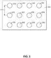
- FIG. 3 is a top down view of the magnetic random access memory structure as seen from line 3 - 3 of FIG. 2 ;
- FIGS. 4-7 are views of a magnetic random access memory structure in various intermediate stages of manufacture, illustrating a method for manufacturing a magnetic random access memory structure
- FIG. 8-11 are views of a magnetic random access memory structure with a mask and electrically conductive layer formation, illustrating a method for testing selected magnetic memory elements of a magnetic random access memory array.
- a magnetic memory element 100 can be in the form of a perpendicular magnetic tunnel junction (pMTJ) memory element.
- the magnetic memory element can include an MTJ 101 that can include a magnetic reference layer 102 , a magnetic free layer 104 and a thin, non-magnetic, electrically insulating magnetic barrier layer 106 located between the magnetic reference layer 102 , and magnetic free layer 104 .
- the barrier layer 106 can be an oxide such as MgO.
- the magnetic reference layer has a magnetization 108 that is fixed in a direction that is preferably perpendicular to the plane of the layers as indicated by arrow 108 .
- the magnetic free layer has a magnetization 110 that can be in either of two directions perpendicular to the plane of the layer 104 . While the magnetization 110 of the free layer remains in either of two directions perpendicular to the plane of the layer 104 in a quiescent state, it can be moved between these two directions as will be described in greater detail herein below.
- the magnetization 110 of the magnetic free layer 104 is in the same direction as the magnetization 108 of the reference layer 102 , the electrical resistance across the layers 102 , 106 , 104 is at a low resistance state.
- the electrical resistance across the layers 102 , 106 , 104 is in a high resistance state.
- the magnetic reference layer 102 can be part of an anti-parallel magnetic pinning structure 112 that can include a magnetic keeper layer 114 , and a non-magnetic, antiparallel coupling layer 116 located between the keeper layer 114 and reference layer 102 .
- the antiparallel coupling layer 116 can be a material such as Ru and can be constructed to have a thickness such that it will ferromagnetically antiparallel couple the layers 114 , 102 .
- the keeper layer 114 can be exchange coupled with a layer of antiferromagnetic material such as IrMn 117 .
- a seed layer 120 may be provided near the bottom of the memory element 100 to initiate a desired crystalline structure in the above deposited layers.
- a capping layer 122 may be provided near the top of the memory element 100 to protect the underlying layers during manufacture, such as during high temperature annealing.
- electrodes 124 , 126 may be provided at the top and bottom of the memory element 100 .
- the electrodes 124 , 126 may be constructed of a non-magnetic, electrically conductive material such as Au and can provide electrical connection with circuitry 128 that can include a current source and can further include circuitry for reading an electrical resistance across the memory element 100 .
- the magnetic free layer 104 has a magnetic anisotropy that causes the magnetization 110 of the free layer 104 to remain stable in one of two directions perpendicular to the plane of the free layer 104 .
- the orientation of the magnetization 110 of the free layer 104 can be switched between these two directions by applying an electrical current through the memory element 100 from the circuitry 128 .
- a current in one direction will cause the memory element to flip to a first orientation, and a current in an opposite direction will cause the magnetization to flip to a second, opposite direction.
- the magnetization 110 is initially oriented in an upward direction in FIG. 1
- applying a current in a downward direction through the element 100 will cause electrons to flow in an opposite direction upward through the element 100 .
- the electrons travelling through the reference layer will become spin polarized as a result of the magnetization 108 of the reference layer 102 . These spin polarized electrons cause a spin torque on the magnetization 110 of the free layer 104 , which causes the magnetization to flip directions.
- the magnetization 110 of the free layer 104 is initially in a downward direction in FIG. 1 , applying an electrical current through the element 100 in an upward direction will cause electrons to flow in an opposite direction, downward through the element 100 .
- the magnetization 110 of the free layer 104 is opposite to the magnetization 108 of the reference layer 102 , the electrons will not be able to pass through the barrier layer 106 .
- the electrons (which have been spin polarized by the magnetization 110 of the free layer 104 , will accumulate at the junction between the free layer 104 and barrier layer 106 . This accumulation of spin polarized electrons causes a spin torque that causes the magnetization 110 of the free layer 104 to flip from a downward direction to an upward direction.
- the memory element 100 may include a spin polarization layer 130 formed above the free layer 104 .
- the spin polarization layer can be separated from the free layer 104 by an exchange coupling layer 132 .
- the spin polarization layer 130 has a magnetic anisotropy that causes it to have a magnetization 134 with a primary component oriented in the in plane direction (e.g. perpendicular to the magnetizations 110 , 108 of the free and reference layers 104 , 102 .
- the magnetization 134 , of the spin polarization layer 130 may either be fixed or can move in a precessional manner as shown in FIG. 100 .
- FIG. 2 shows a side, cross-sectional view of a Magnetic Random Access Memory structure 200 that includes an array of magnetic memory elements 202 .
- the memory elements 202 are formed on a substrate 204 that includes circuitry 206 , such as CMOS circuitry, which can be embedded and formed in the substrate 204 .
- circuitry 206 such as CMOS circuitry
- Each of the magnetic memory elements 202 can be surrounded at their sides by an electrically insulating protective fill layer 208 , such as SiO 2 or alumina.
- a layer of hard mask material 406 can be deposited over the memory element material 404 and a layer of anti-reflective material 408 can be deposited over the hard mask layer 406 .
- the hard mask material 406 can be a material such as SiN, or some other suitable material, and the layer of anti-reflective material 408 can be a bottom anti-reflective coating (BARC) or some other suitable anti-reflective coating.
- a layer of photoresist material such as a spin on glass photoresist 410 is then deposited over the anti-reflective coating 408 .
- a photolithographic process or focused electron beam (e-beam) process can be used to pattern the photoresist 410 , resulting in photoresist mask structure 410 such as that shown in FIG. 5 .
- the photoresist mask 410 is formed to leave mask material in the areas where the magnetic elements are to be formed. Therefore, the photoresist mask 410 can be formed as an array of cylinders of patterned photoresist (shown in side cross-section in FIG. 5 ).
- an electrically insulating fill layer such as SiO 2 or alumina (Al 2 O 3 ) is deposited and a planarization process such as chemical mechanical polishing (CMP) can be performed to form a planar surface.
- CMP chemical mechanical polishing
- the hard mask 408 FIG. 6
- a quick etching such as reactive ion etching can be performed to remove any remaining hard mask, leaving a structure as shown in FIG. 7 .
- FIGS. 8-11 illustrate a process for achieving this without any need to modify the underlying CMOS electronics circuitry.
- a layer of photoresist 802 is deposited over the memory elements and insulation layer.
- the photoresist can be a spin-on glass type photoresist.
- FIG. 11 which shows a cross sectional view similar to FIG. 10 , a layer of electrically conductive metal such as Au, Ag or Cu 1102 is deposited over the entire surface and into the openings in the photoresist mask 802 .
- Testing circuitry 2204 can be electrically connected with the metal 1102 in order to electrically connect with the selected memory elements 404 a .
- the area for making electrical connection (e.g. probing) the memory elements 404 a is much larger, essentially covering the entire surface. This advantageously make it very easy to probe the individual memory elements 404 a without having to physically contact individual memory elements 404 a , which would be far too small to contact using standard probing/testing tooling and techniques.
Abstract
Description
Claims (15)
Priority Applications (1)
| Application Number | Priority Date | Filing Date | Title |
|---|---|---|---|
| US15/859,465 US10607902B2 (en) | 2017-12-30 | 2017-12-30 | Method for measuring proximity effect on high density magnetic tunnel junction devices in a magnetic random access memory device |
Applications Claiming Priority (1)
| Application Number | Priority Date | Filing Date | Title |
|---|---|---|---|
| US15/859,465 US10607902B2 (en) | 2017-12-30 | 2017-12-30 | Method for measuring proximity effect on high density magnetic tunnel junction devices in a magnetic random access memory device |
Publications (2)
| Publication Number | Publication Date |
|---|---|
| US20190206749A1 US20190206749A1 (en) | 2019-07-04 |
| US10607902B2 true US10607902B2 (en) | 2020-03-31 |
Family
ID=67058946
Family Applications (1)
| Application Number | Title | Priority Date | Filing Date |
|---|---|---|---|
| US15/859,465 Active 2038-04-04 US10607902B2 (en) | 2017-12-30 | 2017-12-30 | Method for measuring proximity effect on high density magnetic tunnel junction devices in a magnetic random access memory device |
Country Status (1)
| Country | Link |
|---|---|
| US (1) | US10607902B2 (en) |
Cited By (1)
| Publication number | Priority date | Publication date | Assignee | Title |
|---|---|---|---|---|
| US11283010B2 (en) * | 2018-09-07 | 2022-03-22 | Integrated Silicon Solution, (Cayman) Inc. | Precessional spin current structure for magnetic random access memory with novel capping materials |
Citations (2)
| Publication number | Priority date | Publication date | Assignee | Title |
|---|---|---|---|---|
| US20110076784A1 (en) * | 2009-09-29 | 2011-03-31 | Grandis Inc. | Fabrication of Magnetic Element Arrays |
| US20160315249A1 (en) * | 2015-04-21 | 2016-10-27 | Spin Transfer Technologies, Inc. | Spin transfer torque structure for mram devices having a spin current injection capping layer |
-
2017
- 2017-12-30 US US15/859,465 patent/US10607902B2/en active Active
Patent Citations (2)
| Publication number | Priority date | Publication date | Assignee | Title |
|---|---|---|---|---|
| US20110076784A1 (en) * | 2009-09-29 | 2011-03-31 | Grandis Inc. | Fabrication of Magnetic Element Arrays |
| US20160315249A1 (en) * | 2015-04-21 | 2016-10-27 | Spin Transfer Technologies, Inc. | Spin transfer torque structure for mram devices having a spin current injection capping layer |
Cited By (1)
| Publication number | Priority date | Publication date | Assignee | Title |
|---|---|---|---|---|
| US11283010B2 (en) * | 2018-09-07 | 2022-03-22 | Integrated Silicon Solution, (Cayman) Inc. | Precessional spin current structure for magnetic random access memory with novel capping materials |
Also Published As
| Publication number | Publication date |
|---|---|
| US20190206749A1 (en) | 2019-07-04 |
Similar Documents
| Publication | Publication Date | Title |
|---|---|---|
| US8726491B2 (en) | Method of forming a spin-transfer torque random access memory (STT-RAM) device | |
| RU2469441C2 (en) | Memory cell and method of forming magnetic tunnel junction (mtj) of memory cell | |
| US7884433B2 (en) | High density spin-transfer torque MRAM process | |
| US7825000B2 (en) | Method for integration of magnetic random access memories with improved lithographic alignment to magnetic tunnel junctions | |
| US7602032B2 (en) | Memory having cap structure for magnetoresistive junction and method for structuring the same | |
| US20100240151A1 (en) | Method of double patterning and etching magnetic tunnel junction structures for spin-transfer torque MRAM devices | |
| US6984530B2 (en) | Method of fabricating a MRAM device | |
| US10388860B2 (en) | Method for manufacturing high density magnetic random access memory devices using diamond like carbon hard mask | |
| KR102589614B1 (en) | Magnetic memory device fabrication method using Ru and diamond-like carbon hard masks | |
| US10607902B2 (en) | Method for measuring proximity effect on high density magnetic tunnel junction devices in a magnetic random access memory device | |
| US20050045971A1 (en) | Magnetic memory with self-aligned magnetic keeper structure | |
| CN111480242B (en) | Method for combining NVM class and SRAM class MRAM elements on the same chip | |
| US10868236B2 (en) | Method for manufacturing reduced pitch magnetic random access memory pillar | |
| US10446742B2 (en) | Method for manufacturing a magnetic memory element array using high angle side etch to open top electrical contact | |
| US11723217B2 (en) | Magnetic tunnel junction element with RU hard mask for use in magnetic random-access memory | |
| US11329099B2 (en) | Magnetic memory chip having nvm class and SRAM class MRAM elements on the same chip | |
| US10374153B2 (en) | Method for manufacturing a magnetic memory device by pre-patterning a bottom electrode prior to patterning a magnetic material | |
| US10614867B2 (en) | Patterning of high density small feature size pillar structures | |
| US10615337B2 (en) | Process for creating a high density magnetic tunnel junction array test platform | |
| US10305031B1 (en) | Method for manufacturing a chemical guidance pattern for block copolymer self assembly from photolithographically defined topographic block copolymer guided self assembly | |
| US10312435B1 (en) | Method for manufacturing high density magnetic tunnel junction devices using photolithographic VIAS and chemically guided block copolymer self assembly | |
| US20200098980A1 (en) | Method for forming high density structures with improved resist adhesion to hard mask | |
| US6930370B2 (en) | Memory with conductors between or in communication with storage units |
Legal Events
| Date | Code | Title | Description |
|---|---|---|---|
| FEPP | Fee payment procedure |
Free format text: ENTITY STATUS SET TO UNDISCOUNTED (ORIGINAL EVENT CODE: BIG.); ENTITY STATUS OF PATENT OWNER: LARGE ENTITY |
|
| AS | Assignment |
Owner name: SPIN TRANSFER TECHNOLOGIES, INC., CALIFORNIA Free format text: ASSIGNMENT OF ASSIGNORS INTEREST;ASSIGNORS:BOONE, THOMAS D.;MANANDHAR, PRADEEP;SIGNING DATES FROM 20171221 TO 20171229;REEL/FRAME:044543/0429 |
|
| AS | Assignment |
Owner name: SPIN MEMORY, INC., CALIFORNIA Free format text: CHANGE OF NAME;ASSIGNOR:SPIN TRANSFER TECHNOLOGIES, INC.;REEL/FRAME:048040/0409 Effective date: 20181108 |
|
| STPP | Information on status: patent application and granting procedure in general |
Free format text: RESPONSE TO NON-FINAL OFFICE ACTION ENTERED AND FORWARDED TO EXAMINER |
|
| STPP | Information on status: patent application and granting procedure in general |
Free format text: RESPONSE TO NON-FINAL OFFICE ACTION ENTERED AND FORWARDED TO EXAMINER |
|
| STPP | Information on status: patent application and granting procedure in general |
Free format text: NOTICE OF ALLOWANCE MAILED -- APPLICATION RECEIVED IN OFFICE OF PUBLICATIONS |
|
| STPP | Information on status: patent application and granting procedure in general |
Free format text: PUBLICATIONS -- ISSUE FEE PAYMENT RECEIVED |
|
| STPP | Information on status: patent application and granting procedure in general |
Free format text: PUBLICATIONS -- ISSUE FEE PAYMENT VERIFIED |
|
| STCF | Information on status: patent grant |
Free format text: PATENTED CASE |
|
| AS | Assignment |
Owner name: SPIN (ASSIGNMENT FOR THE BENEFIT OF CREDITORS), LLC, CALIFORNIA Free format text: ASSIGNMENT OF ASSIGNORS INTEREST;ASSIGNOR:SPIN MEMORY, INC.;REEL/FRAME:056927/0038 Effective date: 20210625 |
|
| AS | Assignment |
Owner name: INTEGRATED SILICON SOLUTION, (CAYMAN) INC., CAYMAN ISLANDS Free format text: ASSIGNMENT OF ASSIGNORS INTEREST;ASSIGNOR:SPIN (ASSIGNMENT FOR BENEFIT OF CREDITORS), LLC;REEL/FRAME:057473/0319 Effective date: 20210821 |
|
| MAFP | Maintenance fee payment |
Free format text: PAYMENT OF MAINTENANCE FEE, 4TH YEAR, LARGE ENTITY (ORIGINAL EVENT CODE: M1551); ENTITY STATUS OF PATENT OWNER: LARGE ENTITY Year of fee payment: 4 |