US10601326B2 - Low voltage stress flyback converter with continuous input current - Google Patents
Low voltage stress flyback converter with continuous input current Download PDFInfo
- Publication number
- US10601326B2 US10601326B2 US16/420,556 US201916420556A US10601326B2 US 10601326 B2 US10601326 B2 US 10601326B2 US 201916420556 A US201916420556 A US 201916420556A US 10601326 B2 US10601326 B2 US 10601326B2
- Authority
- US
- United States
- Prior art keywords
- auxiliary
- flyback converter
- switch
- winding
- switching part
- Prior art date
- Legal status (The legal status is an assumption and is not a legal conclusion. Google has not performed a legal analysis and makes no representation as to the accuracy of the status listed.)
- Active
Links
Images


Classifications
-
- H—ELECTRICITY
- H02—GENERATION; CONVERSION OR DISTRIBUTION OF ELECTRIC POWER
- H02M—APPARATUS FOR CONVERSION BETWEEN AC AND AC, BETWEEN AC AND DC, OR BETWEEN DC AND DC, AND FOR USE WITH MAINS OR SIMILAR POWER SUPPLY SYSTEMS; CONVERSION OF DC OR AC INPUT POWER INTO SURGE OUTPUT POWER; CONTROL OR REGULATION THEREOF
- H02M3/00—Conversion of dc power input into dc power output
- H02M3/22—Conversion of dc power input into dc power output with intermediate conversion into ac
- H02M3/24—Conversion of dc power input into dc power output with intermediate conversion into ac by static converters
- H02M3/28—Conversion of dc power input into dc power output with intermediate conversion into ac by static converters using discharge tubes with control electrode or semiconductor devices with control electrode to produce the intermediate ac
- H02M3/325—Conversion of dc power input into dc power output with intermediate conversion into ac by static converters using discharge tubes with control electrode or semiconductor devices with control electrode to produce the intermediate ac using devices of a triode or a transistor type requiring continuous application of a control signal
- H02M3/335—Conversion of dc power input into dc power output with intermediate conversion into ac by static converters using discharge tubes with control electrode or semiconductor devices with control electrode to produce the intermediate ac using devices of a triode or a transistor type requiring continuous application of a control signal using semiconductor devices only
- H02M3/33507—Conversion of dc power input into dc power output with intermediate conversion into ac by static converters using discharge tubes with control electrode or semiconductor devices with control electrode to produce the intermediate ac using devices of a triode or a transistor type requiring continuous application of a control signal using semiconductor devices only with automatic control of the output voltage or current, e.g. flyback converters
-
- H—ELECTRICITY
- H02—GENERATION; CONVERSION OR DISTRIBUTION OF ELECTRIC POWER
- H02M—APPARATUS FOR CONVERSION BETWEEN AC AND AC, BETWEEN AC AND DC, OR BETWEEN DC AND DC, AND FOR USE WITH MAINS OR SIMILAR POWER SUPPLY SYSTEMS; CONVERSION OF DC OR AC INPUT POWER INTO SURGE OUTPUT POWER; CONTROL OR REGULATION THEREOF
- H02M3/00—Conversion of dc power input into dc power output
- H02M3/22—Conversion of dc power input into dc power output with intermediate conversion into ac
- H02M3/24—Conversion of dc power input into dc power output with intermediate conversion into ac by static converters
- H02M3/28—Conversion of dc power input into dc power output with intermediate conversion into ac by static converters using discharge tubes with control electrode or semiconductor devices with control electrode to produce the intermediate ac
- H02M3/325—Conversion of dc power input into dc power output with intermediate conversion into ac by static converters using discharge tubes with control electrode or semiconductor devices with control electrode to produce the intermediate ac using devices of a triode or a transistor type requiring continuous application of a control signal
- H02M3/335—Conversion of dc power input into dc power output with intermediate conversion into ac by static converters using discharge tubes with control electrode or semiconductor devices with control electrode to produce the intermediate ac using devices of a triode or a transistor type requiring continuous application of a control signal using semiconductor devices only
- H02M3/3353—Conversion of dc power input into dc power output with intermediate conversion into ac by static converters using discharge tubes with control electrode or semiconductor devices with control electrode to produce the intermediate ac using devices of a triode or a transistor type requiring continuous application of a control signal using semiconductor devices only having at least two simultaneously operating switches on the input side, e.g. "double forward" or "double (switched) flyback" converter
-
- H—ELECTRICITY
- H02—GENERATION; CONVERSION OR DISTRIBUTION OF ELECTRIC POWER
- H02M—APPARATUS FOR CONVERSION BETWEEN AC AND AC, BETWEEN AC AND DC, OR BETWEEN DC AND DC, AND FOR USE WITH MAINS OR SIMILAR POWER SUPPLY SYSTEMS; CONVERSION OF DC OR AC INPUT POWER INTO SURGE OUTPUT POWER; CONTROL OR REGULATION THEREOF
- H02M1/00—Details of apparatus for conversion
- H02M1/14—Arrangements for reducing ripples from dc input or output
-
- H—ELECTRICITY
- H02—GENERATION; CONVERSION OR DISTRIBUTION OF ELECTRIC POWER
- H02M—APPARATUS FOR CONVERSION BETWEEN AC AND AC, BETWEEN AC AND DC, OR BETWEEN DC AND DC, AND FOR USE WITH MAINS OR SIMILAR POWER SUPPLY SYSTEMS; CONVERSION OF DC OR AC INPUT POWER INTO SURGE OUTPUT POWER; CONTROL OR REGULATION THEREOF
- H02M3/00—Conversion of dc power input into dc power output
- H02M3/22—Conversion of dc power input into dc power output with intermediate conversion into ac
- H02M3/24—Conversion of dc power input into dc power output with intermediate conversion into ac by static converters
- H02M3/28—Conversion of dc power input into dc power output with intermediate conversion into ac by static converters using discharge tubes with control electrode or semiconductor devices with control electrode to produce the intermediate ac
- H02M3/325—Conversion of dc power input into dc power output with intermediate conversion into ac by static converters using discharge tubes with control electrode or semiconductor devices with control electrode to produce the intermediate ac using devices of a triode or a transistor type requiring continuous application of a control signal
- H02M3/335—Conversion of dc power input into dc power output with intermediate conversion into ac by static converters using discharge tubes with control electrode or semiconductor devices with control electrode to produce the intermediate ac using devices of a triode or a transistor type requiring continuous application of a control signal using semiconductor devices only
- H02M3/33507—Conversion of dc power input into dc power output with intermediate conversion into ac by static converters using discharge tubes with control electrode or semiconductor devices with control electrode to produce the intermediate ac using devices of a triode or a transistor type requiring continuous application of a control signal using semiconductor devices only with automatic control of the output voltage or current, e.g. flyback converters
- H02M3/33523—Conversion of dc power input into dc power output with intermediate conversion into ac by static converters using discharge tubes with control electrode or semiconductor devices with control electrode to produce the intermediate ac using devices of a triode or a transistor type requiring continuous application of a control signal using semiconductor devices only with automatic control of the output voltage or current, e.g. flyback converters with galvanic isolation between input and output of both the power stage and the feedback loop
-
- H—ELECTRICITY
- H02—GENERATION; CONVERSION OR DISTRIBUTION OF ELECTRIC POWER
- H02M—APPARATUS FOR CONVERSION BETWEEN AC AND AC, BETWEEN AC AND DC, OR BETWEEN DC AND DC, AND FOR USE WITH MAINS OR SIMILAR POWER SUPPLY SYSTEMS; CONVERSION OF DC OR AC INPUT POWER INTO SURGE OUTPUT POWER; CONTROL OR REGULATION THEREOF
- H02M1/00—Details of apparatus for conversion
- H02M1/0003—Details of control, feedback or regulation circuits
-
- H—ELECTRICITY
- H02—GENERATION; CONVERSION OR DISTRIBUTION OF ELECTRIC POWER
- H02M—APPARATUS FOR CONVERSION BETWEEN AC AND AC, BETWEEN AC AND DC, OR BETWEEN DC AND DC, AND FOR USE WITH MAINS OR SIMILAR POWER SUPPLY SYSTEMS; CONVERSION OF DC OR AC INPUT POWER INTO SURGE OUTPUT POWER; CONTROL OR REGULATION THEREOF
- H02M1/00—Details of apparatus for conversion
- H02M1/44—Circuits or arrangements for compensating for electromagnetic interference in converters or inverters
-
- H02M2001/0003—
Definitions
- the present disclosure relates to a flyback converter.
- FIG. 1 is a circuit diagram showing a conventional flyback converter.
- the flyback type scheme as illustrated in FIG. 1 may be used as a low-power DC-DC converter of 50 W or less used for secondary power conversion of geostationary satellites.
- Such flyback converter has an input current in a pulse shape and thus requires an EMI filter to meet the satellite electro magnetic interference (EMI) requirements.
- EMI satellite electro magnetic interference
- the voltage stress of a switch for the converter is also increasing.
- An increase in the voltage stress of the switch leads to a demand for a switch that has a larger conduction resistance, which causes an increase in converter conduction loss.
- the switching loss also increases for each switching operation, which is caused by overlapping of the switch voltage and the current. In this way, the power loss at the switch can be increased when designing a high-frequency switching required for miniaturization of the converter size and therefore, it is very important to reduce the voltage stress when designing a high-density converter.
- a flyback converter including a transformer comprising a primary winding and a secondary winding, the transformer for transforming a power inputted from an input power supply and outputting the transformed power, a switching part having one end connected to the primary winding and the other end connected to a ground of the input power supply, and an auxiliary circuit including an auxiliary capacitor, and an auxiliary winding coupled to the primary winding.
- the auxiliary circuit may be connected to the switching part in parallel.
- the auxiliary capacitor and the auxiliary winding may be connected to each other in series.
- the auxiliary winding may be connected to a contact of the primary winding and the switching part, and one end of the auxiliary capacitor may be connected to the other end of the switching part.
- the flyback converter may additionally include a clamping diode
- the switching part may include a first switch and a second switch connected to each other in series, an anode of the clamping diode may be connected to a contact of the first switch and the second switch, and a cathode of the clamping diode may be connected to a contact of the auxiliary winding and the auxiliary capacitor.
- the auxiliary winding and the primary winding may have a same number of windings.
- the flyback converter may be operated based on a first mode and a second mode.
- the switching part may be turned on and energy may be stored in a magnetizing inductance of the transformer.
- the switching unit may be turned off and the energy stored in the magnetizing inductance of the transformer may be transferred to a secondary side.
- FIG. 1 is a circuit diagram showing a conventional flyback converter
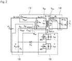
- FIG. 2 is a circuit diagram showing a flyback converter according to an embodiment of the present disclosure
- FIG. 3 is a diagram illustrating a conduction path in a first mode of a flyback converter circuit according to an embodiment of the present disclosure
- FIG. 4 is a diagram illustrating a conduction path in a second mode of a flyback converter circuit according to an embodiment of the present disclosure
- FIG. 5 is a circuit diagram showing a flyback converter according to another embodiment of the present disclosure.
- FIG. 6 is a diagram showing the main operation waveforms of the flyback converter circuit of FIG. 2 ;
- FIG. 7 is a diagram showing the main operation waveforms of the flyback converter circuit of FIG. 5 ;
- FIG. 8A-8C are diagrams showing simulation results of an input current and a switch voltage of a flyback converter circuit according to the present disclosure.
- FIG. 9A-9B are diagrams showing simulation results of an input current and a switch voltage of the conventional flyback converter.
- FIG. 2 is a circuit diagram of a flyback converter according to an embodiment of the present disclosure.
- the flyback converter may include a transformer 110 , a switching part 120 , an auxiliary circuit 130 , and a rectifier 140 .
- the transformer 110 includes a primary winding N pri and a secondary winding N sec , and transforms an input power V in according to the switching operation of the switching part 120 by a winding ratio (N:1) set by the number of windings of the primary winding N pri and the secondary winding N sec and outputs the transformed power.
- the primary winding N pri may have a leakage inductance L k1 and a magnetizing inductance L m .
- the switching part 120 may have one end connected to the primary winding N pri and the other end connected to a ground of the input power supply V in .
- the switching part 120 may include a first switch M 1 and a second switch M 2 that are connected to each other in series.
- the first switch M 11 and the second switch M 12 may be implemented as a power field effect transistor (FET), or may be implemented as other power switch devices such as MOSFET and so on, depending on embodiments.
- FET power field effect transistor
- the auxiliary circuit 130 includes an auxiliary winding N aux coupled to the primary winding N pri and an auxiliary capacitor C b and may be connected in parallel to the switching part 120 in parallel.
- One end of the auxiliary winding N aux may be connected to a contact of the primary winding N pri and the switching part 120 and the other end may be connected to the auxiliary capacitor C b .
- the auxiliary winding N aux may have the leakage inductance L k3 .
- the auxiliary winding N aux has the same number of windings (N) as the primary winding N pri and may be connected so that the polarity is opposite to one of the secondary winding.
- One end of the auxiliary capacitor C b may be connected to the other end of the switching part 120 and the other end may be connected to the auxiliary winding N aux .
- the flyback converter according to the present disclosure may further include a clamping diode D cl for connecting a contact of the auxiliary winding N aux and the auxiliary capacitor C b to a contact of the first switch M 1 and the second switch M 2 .
- a clamping diode D cl for connecting a contact of the auxiliary winding N aux and the auxiliary capacitor C b to a contact of the first switch M 1 and the second switch M 2 .
- an anode of the clamping diode D cl may be connected to the contact of the first switch M 1 and the second switch M 2
- a cathode of the clamping diode D cl may be connected to the contact of the auxiliary winding N aux and the auxiliary capacitor C b .
- the rectifier 140 may rectify the power outputted from the transformer 110 and output the rectified power to the load R o and may include an output diode D o and an output capacitor C o .
- FIG. 3 is a diagram illustrating a conduction path in a first mode of a flyback converter circuit according to an embodiment of the present disclosure.
- the flyback converter circuit may have a current conduction path as illustrated in FIG. 3 in a first mode in which the switching part 120 is turned on (i.e., both the first switch M 1 and the second switch M 2 are turned on).
- the first mode there are two conduction paths ⁇ circle around ( 1 ) ⁇ and ⁇ circle around ( 2 ) ⁇ on the primary circuit side.
- energy is stored in the magnetizing inductance L m of the transformer 110 .
- the first conduction path ⁇ circle around ( 1 ) ⁇ includes the input power V in , the primary side of the transformer 110 , the switching part 120 , and the input power V in
- the second conduction path 2 includes the auxiliary capacitor C b , the auxiliary winding N aux , the switching part 120 , and the auxiliary capacitor C b .
- the current conduction path on the secondary circuit side includes an output capacitor C o , a load R o , and an output capacitor C o .
- the main voltage in the first mode is described below.
- the input voltage V in is divided and applied to the leakage inductance L k1 and the magnetizing inductance L m .
- the voltage V pri across both ends of the magnetizing inductance L m is equal to the voltage V aux applied to the auxiliary winding N aux .
- the voltage V Cb applied to the primary-side auxiliary capacitor C b is equal to the input voltage V in .
- the voltage V Cb is divided and applied to the leakage inductance L k3 and the auxiliary winding N aux .
- the voltages V Lk1 and V Lk3 of the primary-side and the auxiliary-side leakage inductances L k1 and L k3 are also equal to each other.
- the secondary-side voltage V sec of the transformer 110 is 0 V due to the output diode D o on the secondary circuit side blocking the current flow.
- the currents of the primary side and the secondary side are expressed as follows.
- i main_sw ( t ) i Lm ( t )
- i Lm ( t ) i in ( t )+ i aux ( t )
- the slopes of the inductor currents are inversely proportional to the inductances, when the same voltages are applied to L k1 and L k3 . Therefore, when L k1 >>L k3 , an amount of variations of i in is significantly smaller than that of f aux . Thus, when L k1 /L k3 is sufficiently large, i in flows similarly to DC current with a significantly reduced ripple, while the remainder of ripple current flows through the auxiliary winding.
- i o (t) is a discharge current of the output capacitor C o , and its slope is determined by the output resistance R o and the output capacitor C o .
- FIG. 4 is a diagram illustrating a conduction path in a second mode of a flyback converter circuit according to an embodiment of the present disclosure.
- the primary circuit side and the secondary circuit side may have the current conduction paths as shown in FIG. 4 , respectively, in the second mode in which the switching part 120 is turned off (i.e., both the first switch M 1 and the second switch M 2 are turned off).
- the energy stored in the magnetizing inductance L m of the transformer 110 is transferred to the secondary circuit side.
- the conduction path on the primary circuit side includes the input power V in , the primary side of the transformer 110 , the auxiliary winding N aux , the auxiliary capacitor C b , and the input power V in
- the current conduction path on the secondary circuit side includes the secondary side of the transformer 110 , the output diode D o , the (output capacitor C o //load R o ) and the secondary side of the transformer 110 .
- the input current i in flows to the auxiliary winding N aux to charge the auxiliary capacitor C b for achieving the current-second balance of C b . Therefore the current i in and current i aux have the same magnitude according to the Kirchhoff's Current Law (KCL).
- KCL Kirchhoff's Current Law
- the voltage across both ends of the magnetizing inductance L m is a negative value so that the secondary side output diode D o is in conductive state, in which case the energy stored in the magnetizing inductance L m is transferred to the secondary side so that the current i Lm decreases to the initial value of the first mode to achieve the voltage-second balance of L m .
- the main voltage in the second mode is as follows.
- the voltage V ds of the primary-side switching part is divided and applied to the first switch M 1 and the second switch M 2 as V ds1 and V ds2 , respectively.
- the currents of the primary side and the secondary side are expressed as follows.
- the current f aux of the auxiliary winding N aux flows toward the auxiliary capacitor C b at a constant value to charge the auxiliary capacitor C b .
- the input current i in flows at a constant value like a direct current (DC).
- FIG. 5 is a circuit diagram showing a flyback converter according to another embodiment of the present disclosure.
- the flyback converter according to another embodiment may include a transformer 110 , a switching part 120 , an auxiliary circuit 130 , and a rectifier 140 .
- the only difference from the embodiment of FIG. 2 is that the switching part 120 includes one switch M and the clamping diode D cl is not included.
- FIG. 6 is a diagram showing the main operation waveforms of the flyback converter circuit of FIG. 2 .
- FIG. 7 is a diagram showing the main operation waveforms of the flyback converter circuit of FIG. 5 .
- the main operation waveform of the flyback converter according to the embodiments illustrated in FIGS. 2 and 5 can be observed in the first mode in which the switches M, M 1 , and M 2 are turned on for the time period D and in the second mode in which the switches M, M 1 , and M 2 are turned off for the time period 1-D.
- the ripple of the input current i in is greatly reduced and the current flows continuously like a direct current (DC). Meanwhile, voltage stresses of the main switches in the FIG. 2 are clamped to ‘0.5*(V in +NV o )’, respectively, which are relieved to the half level comparing to one of FIG. 5 .
- FIG. 8A-8C are diagrams showing simulation results of an input current and a switch voltage of a flyback converter circuit according to the present disclosure.
- FIG. 9A-9B are diagrams showing simulation results of an input current and a switch voltage of a conventional flyback converter circuit.
- FIG. 8A shows the simulation result of the input current i in of the flyback converter circuit according to the present disclosure
- FIG. 8B shows the simulation result of the switch voltage of the flyback converter circuit of FIG. 2
- FIG. 8C shows the simulation result of the switch voltage of the flyback converter circuit of FIG. 5
- FIG. 9A shows the simulation result of the input current i in of a conventional flyback converter circuit
- FIG. 9B shows the simulation result of the switch voltage of the conventional flyback converter circuit.
- the ripple of the input current i in in the flyback converter according to the present disclosure is greatly reduced compared to the ripple of the input current i in in the conventional flyback converter and that the current flows continuously like DC. Also it can be seen that the voltage stress of the switch in the flyback converter according to the present disclosure is relieved to the half level as compared with the conventional flyback converter.
Landscapes
- Engineering & Computer Science (AREA)
- Power Engineering (AREA)
- Dc-Dc Converters (AREA)
Abstract
Description
i main_sw(t)=i Lm(t)
i Lm(t)=i in(t)+i aux(t)
i Do=0
-
- Primary-side transformer voltage: Vpri=Vaux=−VO/N
- Voltage VCb of the primary-side auxiliary capacitor Cb is equal to Vin
- Voltage VLk1 of the primary-side leakage inductance is equal to VLk3 of the auxiliary-side leakage inductance
- Voltage Vds of the primary-side switching part: Vin−(Vpri VLk1)
-
- Voltage Vsec on the secondary side: −VO
i main_sw(t)=0
i Lm(t)=i pri(t)+i in(t)+i aux(t)
i in =−i aux(t)
i Do(t)=i pri(t)·N
Claims (3)
Applications Claiming Priority (2)
| Application Number | Priority Date | Filing Date | Title |
|---|---|---|---|
| KR10-2018-0059756 | 2018-05-25 | ||
| KR1020180059756A KR102075470B1 (en) | 2018-05-25 | 2018-05-25 | A flyback converter |
Publications (2)
| Publication Number | Publication Date |
|---|---|
| US20190363632A1 US20190363632A1 (en) | 2019-11-28 |
| US10601326B2 true US10601326B2 (en) | 2020-03-24 |
Family
ID=66630267
Family Applications (1)
| Application Number | Title | Priority Date | Filing Date |
|---|---|---|---|
| US16/420,556 Active US10601326B2 (en) | 2018-05-25 | 2019-05-23 | Low voltage stress flyback converter with continuous input current |
Country Status (3)
| Country | Link |
|---|---|
| US (1) | US10601326B2 (en) |
| EP (1) | EP3573224A1 (en) |
| KR (1) | KR102075470B1 (en) |
Families Citing this family (1)
| Publication number | Priority date | Publication date | Assignee | Title |
|---|---|---|---|---|
| CN114204822B (en) * | 2021-12-10 | 2024-01-26 | 杭州优特电源有限公司 | High-voltage direct-current auxiliary power supply circuit |
Citations (11)
| Publication number | Priority date | Publication date | Assignee | Title |
|---|---|---|---|---|
| US5694302A (en) | 1996-08-20 | 1997-12-02 | Compaq Computer Corporation | Passive clamp and ripple control for buck boost converter |
| US6295213B1 (en) * | 2000-02-14 | 2001-09-25 | Astec International Limited | Circuit for efficiently clamping a power converter's reset voltage and for providing auxiliary power |
| KR20100027931A (en) | 2008-09-03 | 2010-03-11 | 주식회사 아이디코리아 | Active clamp forward converter |
| US8000112B2 (en) * | 2008-04-11 | 2011-08-16 | Flextronics Ap, Llc | Active snubber for transition mode power converter |
| KR101248807B1 (en) | 2011-08-05 | 2013-04-01 | 주식회사 동부하이텍 | Isolation-type flyback converter for light emitting diode driver |
| US9048738B2 (en) * | 2003-01-15 | 2015-06-02 | On-Bright Electronics (Shanghai) Co., Ltd. | Systems and methods for zero voltage switching in power conversion systems |
| US9326336B2 (en) * | 2014-02-12 | 2016-04-26 | Dialog Semiconductor (Uk) Limited | Dual switcher flyback structure for LED driver |
| US20180062529A1 (en) * | 2016-08-31 | 2018-03-01 | Delta Electronics, Inc. | Converter and control method thereof |
| US9935556B1 (en) * | 2017-01-27 | 2018-04-03 | Semiconductor Components Industries, Llc | Primary-side control of resonant converters |
| US9991803B1 (en) * | 2017-01-18 | 2018-06-05 | Semiconductor Components Industries, Llc | Reduction of electromagnetic interference in a flyback converter |
| US20190173385A1 (en) * | 2017-12-01 | 2019-06-06 | Korea Aerospace Research Institute | Dc-dc converter |
Family Cites Families (9)
| Publication number | Priority date | Publication date | Assignee | Title |
|---|---|---|---|---|
| US5038263A (en) * | 1990-01-03 | 1991-08-06 | Eg&G Power Systems, Inc. | Ripple current reduction circuit |
| US6473318B1 (en) * | 2000-11-20 | 2002-10-29 | Koninklijke Philips Electronics N.V. | Leakage energy recovering system and method for flyback converter |
| US6314002B1 (en) * | 2000-11-20 | 2001-11-06 | Philips Electronics North America Corporation | Voltage clamping system and method for a DC/DC power converter |
| TWI309916B (en) * | 2006-07-26 | 2009-05-11 | Ching Shan Leu | Low voltage stress power inversion and rectification circuits |
| US20110199802A1 (en) * | 2008-04-15 | 2011-08-18 | National Taiwan University Of Science And Technology | Single ended power converters operating over 50% duty cycle |
| JP5018960B2 (en) * | 2008-07-23 | 2012-09-05 | 株式会社村田製作所 | Isolated switching power supply |
| CN101741258B (en) * | 2010-01-19 | 2012-05-09 | 魏其萃 | Isolative current regulation type direct current-direct current converter |
| US9825544B2 (en) * | 2014-04-01 | 2017-11-21 | Securaplane Technologies, Inc. | Power converters |
| TWI536727B (en) * | 2014-05-06 | 2016-06-01 | 國立清華大學 | Pulsating current ripple cancelling circuit and conversion system |
-
2018
- 2018-05-25 KR KR1020180059756A patent/KR102075470B1/en active IP Right Grant
-
2019
- 2019-05-22 EP EP19175984.4A patent/EP3573224A1/en not_active Withdrawn
- 2019-05-23 US US16/420,556 patent/US10601326B2/en active Active
Patent Citations (12)
| Publication number | Priority date | Publication date | Assignee | Title |
|---|---|---|---|---|
| US5694302A (en) | 1996-08-20 | 1997-12-02 | Compaq Computer Corporation | Passive clamp and ripple control for buck boost converter |
| US6295213B1 (en) * | 2000-02-14 | 2001-09-25 | Astec International Limited | Circuit for efficiently clamping a power converter's reset voltage and for providing auxiliary power |
| US9048738B2 (en) * | 2003-01-15 | 2015-06-02 | On-Bright Electronics (Shanghai) Co., Ltd. | Systems and methods for zero voltage switching in power conversion systems |
| US8000112B2 (en) * | 2008-04-11 | 2011-08-16 | Flextronics Ap, Llc | Active snubber for transition mode power converter |
| KR20100027931A (en) | 2008-09-03 | 2010-03-11 | 주식회사 아이디코리아 | Active clamp forward converter |
| KR101248807B1 (en) | 2011-08-05 | 2013-04-01 | 주식회사 동부하이텍 | Isolation-type flyback converter for light emitting diode driver |
| US9326336B2 (en) * | 2014-02-12 | 2016-04-26 | Dialog Semiconductor (Uk) Limited | Dual switcher flyback structure for LED driver |
| US20180062529A1 (en) * | 2016-08-31 | 2018-03-01 | Delta Electronics, Inc. | Converter and control method thereof |
| US10177668B2 (en) * | 2016-08-31 | 2019-01-08 | Delta Electronics, Inc. | Converter and control method thereof |
| US9991803B1 (en) * | 2017-01-18 | 2018-06-05 | Semiconductor Components Industries, Llc | Reduction of electromagnetic interference in a flyback converter |
| US9935556B1 (en) * | 2017-01-27 | 2018-04-03 | Semiconductor Components Industries, Llc | Primary-side control of resonant converters |
| US20190173385A1 (en) * | 2017-12-01 | 2019-06-06 | Korea Aerospace Research Institute | Dc-dc converter |
Also Published As
| Publication number | Publication date |
|---|---|
| EP3573224A1 (en) | 2019-11-27 |
| KR102075470B1 (en) | 2020-02-10 |
| KR20190134295A (en) | 2019-12-04 |
| US20190363632A1 (en) | 2019-11-28 |
Similar Documents
| Publication | Publication Date | Title |
|---|---|---|
| US5943224A (en) | Post regulator with energy recovery snubber and power supply employing the same | |
| US6501193B1 (en) | Power converter having regulated dual outputs | |
| US7787261B2 (en) | Intermediate bus architecture with a quasi-regulated bus converter | |
| US6982887B2 (en) | DC-DC converter with coupled-inductors current-doubler | |
| US8345450B2 (en) | Resonant converter having over-current protection apparatus and controlling method thereof | |
| US6272027B1 (en) | AC active clamp for isolated power factor corrector and method of operating the same | |
| US10686387B2 (en) | Multi-transformer LLC resonant converter circuit | |
| US6002597A (en) | Synchronous rectifier having dynamically adjustable current rating and method of operation thereof | |
| US6778412B2 (en) | Synchronous converter with reverse current protection through variable inductance | |
| JP2005160217A (en) | Switching power supply | |
| US11527959B2 (en) | Control method of power conversion device | |
| US11664728B2 (en) | Power conversion device | |
| US7184287B2 (en) | Rectifier clamping circuit with reverse energy recovery | |
| US11784560B2 (en) | Power conversion circuit | |
| KR20220152987A (en) | Power supplier and power supply method using the same | |
| US6487094B1 (en) | High efficiency DC-DC power converter | |
| US8711588B1 (en) | Power supply device | |
| US10601326B2 (en) | Low voltage stress flyback converter with continuous input current | |
| US20110310638A1 (en) | Power factor corrector and driving method thereof | |
| US6995547B2 (en) | Low loss boost converter | |
| KR101958276B1 (en) | Active clamp forward converter | |
| KR101813778B1 (en) | Hybride type LED Power Supply | |
| Han et al. | Efficiency optimized asymmetric half-bridge converter with hold-up time compensation | |
| KR101980021B1 (en) | High efficiency multi-output converter with asymmetric powering | |
| KR20190098368A (en) | Active Clamp Forward Converter And Method Of Driving The Same |
Legal Events
| Date | Code | Title | Description |
|---|---|---|---|
| AS | Assignment |
Owner name: KOOKMIN UNIVERSITY INDUSTRY ACADEMY COOPERATION FO Free format text: ASSIGNMENT OF ASSIGNORS INTEREST;ASSIGNORS:LEE, NA YOUNG;CHOI, JAE DONG;HAN, SANG KYOO;AND OTHERS;REEL/FRAME:049267/0506 Effective date: 20190514 Owner name: KOREA AEROSPACE RESEARCH INSTITUTE, KOREA, REPUBLI Free format text: ASSIGNMENT OF ASSIGNORS INTEREST;ASSIGNORS:LEE, NA YOUNG;CHOI, JAE DONG;HAN, SANG KYOO;AND OTHERS;REEL/FRAME:049267/0506 Effective date: 20190514 Owner name: KOOKMIN UNIVERSITY INDUSTRY ACADEMY COOPERATION FOUNDATION, KOREA, REPUBLIC OF Free format text: ASSIGNMENT OF ASSIGNORS INTEREST;ASSIGNORS:LEE, NA YOUNG;CHOI, JAE DONG;HAN, SANG KYOO;AND OTHERS;REEL/FRAME:049267/0506 Effective date: 20190514 Owner name: KOREA AEROSPACE RESEARCH INSTITUTE, KOREA, REPUBLIC OF Free format text: ASSIGNMENT OF ASSIGNORS INTEREST;ASSIGNORS:LEE, NA YOUNG;CHOI, JAE DONG;HAN, SANG KYOO;AND OTHERS;REEL/FRAME:049267/0506 Effective date: 20190514 |
|
| FEPP | Fee payment procedure |
Free format text: ENTITY STATUS SET TO UNDISCOUNTED (ORIGINAL EVENT CODE: BIG.); ENTITY STATUS OF PATENT OWNER: LARGE ENTITY |
|
| STPP | Information on status: patent application and granting procedure in general |
Free format text: NON FINAL ACTION MAILED |
|
| STPP | Information on status: patent application and granting procedure in general |
Free format text: NOTICE OF ALLOWANCE MAILED -- APPLICATION RECEIVED IN OFFICE OF PUBLICATIONS |
|
| STPP | Information on status: patent application and granting procedure in general |
Free format text: PUBLICATIONS -- ISSUE FEE PAYMENT VERIFIED |
|
| STCF | Information on status: patent grant |
Free format text: PATENTED CASE |
|
| MAFP | Maintenance fee payment |
Free format text: PAYMENT OF MAINTENANCE FEE, 4TH YEAR, LARGE ENTITY (ORIGINAL EVENT CODE: M1551); ENTITY STATUS OF PATENT OWNER: LARGE ENTITY Year of fee payment: 4 |