US10600762B2 - Apparatuses comprising semiconductor dies in face-to-face arrangements - Google Patents

Apparatuses comprising semiconductor dies in face-to-face arrangements Download PDF

Info

Publication number
US10600762B2
US10600762B2 US16/447,749 US201916447749A US10600762B2 US 10600762 B2 US10600762 B2 US 10600762B2 US 201916447749 A US201916447749 A US 201916447749A US 10600762 B2 US10600762 B2 US 10600762B2
Authority
US
United States
Prior art keywords
die
face
regions
region
dies
Prior art date
Legal status (The legal status is an assumption and is not a legal conclusion. Google has not performed a legal analysis and makes no representation as to the accuracy of the status listed.)
Active
Application number
US16/447,749
Other versions
US20190304955A1 (en
Inventor
Dai Sasaki
Mitsuaki Katagiri
Satoshi Isa
Current Assignee (The listed assignees may be inaccurate. Google has not performed a legal analysis and makes no representation or warranty as to the accuracy of the list.)
Micron Technology Inc
Original Assignee
Micron Technology Inc
Priority date (The priority date is an assumption and is not a legal conclusion. Google has not performed a legal analysis and makes no representation as to the accuracy of the date listed.)
Filing date
Publication date
Application filed by Micron Technology Inc filed Critical Micron Technology Inc
Priority to US16/447,749 priority Critical patent/US10600762B2/en
Publication of US20190304955A1 publication Critical patent/US20190304955A1/en
Application granted granted Critical
Publication of US10600762B2 publication Critical patent/US10600762B2/en
Active legal-status Critical Current
Anticipated expiration legal-status Critical

Links

Images

Classifications

    • HELECTRICITY
    • H01ELECTRIC ELEMENTS
    • H01LSEMICONDUCTOR DEVICES NOT COVERED BY CLASS H10
    • H01L22/00Testing or measuring during manufacture or treatment; Reliability measurements, i.e. testing of parts without further processing to modify the parts as such; Structural arrangements therefor
    • H01L22/30Structural arrangements specially adapted for testing or measuring during manufacture or treatment, or specially adapted for reliability measurements
    • H01L22/32Additional lead-in metallisation on a device or substrate, e.g. additional pads or pad portions, lines in the scribe line, sacrificed conductors
    • HELECTRICITY
    • H01ELECTRIC ELEMENTS
    • H01LSEMICONDUCTOR DEVICES NOT COVERED BY CLASS H10
    • H01L23/00Details of semiconductor or other solid state devices
    • H01L23/52Arrangements for conducting electric current within the device in operation from one component to another, i.e. interconnections, e.g. wires, lead frames
    • H01L23/522Arrangements for conducting electric current within the device in operation from one component to another, i.e. interconnections, e.g. wires, lead frames including external interconnections consisting of a multilayer structure of conductive and insulating layers inseparably formed on the semiconductor body
    • H01L23/528Geometry or layout of the interconnection structure
    • HELECTRICITY
    • H01ELECTRIC ELEMENTS
    • H01LSEMICONDUCTOR DEVICES NOT COVERED BY CLASS H10
    • H01L24/00Arrangements for connecting or disconnecting semiconductor or solid-state bodies; Methods or apparatus related thereto
    • H01L24/01Means for bonding being attached to, or being formed on, the surface to be connected, e.g. chip-to-package, die-attach, "first-level" interconnects; Manufacturing methods related thereto
    • H01L24/02Bonding areas ; Manufacturing methods related thereto
    • H01L24/04Structure, shape, material or disposition of the bonding areas prior to the connecting process
    • H01L24/06Structure, shape, material or disposition of the bonding areas prior to the connecting process of a plurality of bonding areas
    • HELECTRICITY
    • H01ELECTRIC ELEMENTS
    • H01LSEMICONDUCTOR DEVICES NOT COVERED BY CLASS H10
    • H01L24/00Arrangements for connecting or disconnecting semiconductor or solid-state bodies; Methods or apparatus related thereto
    • H01L24/01Means for bonding being attached to, or being formed on, the surface to be connected, e.g. chip-to-package, die-attach, "first-level" interconnects; Manufacturing methods related thereto
    • H01L24/10Bump connectors ; Manufacturing methods related thereto
    • H01L24/12Structure, shape, material or disposition of the bump connectors prior to the connecting process
    • H01L24/14Structure, shape, material or disposition of the bump connectors prior to the connecting process of a plurality of bump connectors
    • HELECTRICITY
    • H01ELECTRIC ELEMENTS
    • H01LSEMICONDUCTOR DEVICES NOT COVERED BY CLASS H10
    • H01L24/00Arrangements for connecting or disconnecting semiconductor or solid-state bodies; Methods or apparatus related thereto
    • H01L24/01Means for bonding being attached to, or being formed on, the surface to be connected, e.g. chip-to-package, die-attach, "first-level" interconnects; Manufacturing methods related thereto
    • H01L24/10Bump connectors ; Manufacturing methods related thereto
    • H01L24/15Structure, shape, material or disposition of the bump connectors after the connecting process
    • H01L24/17Structure, shape, material or disposition of the bump connectors after the connecting process of a plurality of bump connectors
    • HELECTRICITY
    • H01ELECTRIC ELEMENTS
    • H01LSEMICONDUCTOR DEVICES NOT COVERED BY CLASS H10
    • H01L25/00Assemblies consisting of a plurality of individual semiconductor or other solid state devices ; Multistep manufacturing processes thereof
    • H01L25/03Assemblies consisting of a plurality of individual semiconductor or other solid state devices ; Multistep manufacturing processes thereof all the devices being of a type provided for in the same subgroup of groups H01L27/00 - H01L33/00, or in a single subclass of H10K, H10N, e.g. assemblies of rectifier diodes
    • H01L25/04Assemblies consisting of a plurality of individual semiconductor or other solid state devices ; Multistep manufacturing processes thereof all the devices being of a type provided for in the same subgroup of groups H01L27/00 - H01L33/00, or in a single subclass of H10K, H10N, e.g. assemblies of rectifier diodes the devices not having separate containers
    • H01L25/065Assemblies consisting of a plurality of individual semiconductor or other solid state devices ; Multistep manufacturing processes thereof all the devices being of a type provided for in the same subgroup of groups H01L27/00 - H01L33/00, or in a single subclass of H10K, H10N, e.g. assemblies of rectifier diodes the devices not having separate containers the devices being of a type provided for in group H01L27/00
    • H01L25/0657Stacked arrangements of devices
    • HELECTRICITY
    • H01ELECTRIC ELEMENTS
    • H01LSEMICONDUCTOR DEVICES NOT COVERED BY CLASS H10
    • H01L2224/00Indexing scheme for arrangements for connecting or disconnecting semiconductor or solid-state bodies and methods related thereto as covered by H01L24/00
    • H01L2224/01Means for bonding being attached to, or being formed on, the surface to be connected, e.g. chip-to-package, die-attach, "first-level" interconnects; Manufacturing methods related thereto
    • H01L2224/02Bonding areas; Manufacturing methods related thereto
    • H01L2224/023Redistribution layers [RDL] for bonding areas
    • H01L2224/0237Disposition of the redistribution layers
    • H01L2224/02371Disposition of the redistribution layers connecting the bonding area on a surface of the semiconductor or solid-state body with another surface of the semiconductor or solid-state body
    • HELECTRICITY
    • H01ELECTRIC ELEMENTS
    • H01LSEMICONDUCTOR DEVICES NOT COVERED BY CLASS H10
    • H01L2224/00Indexing scheme for arrangements for connecting or disconnecting semiconductor or solid-state bodies and methods related thereto as covered by H01L24/00
    • H01L2224/01Means for bonding being attached to, or being formed on, the surface to be connected, e.g. chip-to-package, die-attach, "first-level" interconnects; Manufacturing methods related thereto
    • H01L2224/02Bonding areas; Manufacturing methods related thereto
    • H01L2224/04Structure, shape, material or disposition of the bonding areas prior to the connecting process
    • H01L2224/0401Bonding areas specifically adapted for bump connectors, e.g. under bump metallisation [UBM]
    • HELECTRICITY
    • H01ELECTRIC ELEMENTS
    • H01LSEMICONDUCTOR DEVICES NOT COVERED BY CLASS H10
    • H01L2224/00Indexing scheme for arrangements for connecting or disconnecting semiconductor or solid-state bodies and methods related thereto as covered by H01L24/00
    • H01L2224/01Means for bonding being attached to, or being formed on, the surface to be connected, e.g. chip-to-package, die-attach, "first-level" interconnects; Manufacturing methods related thereto
    • H01L2224/02Bonding areas; Manufacturing methods related thereto
    • H01L2224/04Structure, shape, material or disposition of the bonding areas prior to the connecting process
    • H01L2224/04042Bonding areas specifically adapted for wire connectors, e.g. wirebond pads
    • HELECTRICITY
    • H01ELECTRIC ELEMENTS
    • H01LSEMICONDUCTOR DEVICES NOT COVERED BY CLASS H10
    • H01L2224/00Indexing scheme for arrangements for connecting or disconnecting semiconductor or solid-state bodies and methods related thereto as covered by H01L24/00
    • H01L2224/01Means for bonding being attached to, or being formed on, the surface to be connected, e.g. chip-to-package, die-attach, "first-level" interconnects; Manufacturing methods related thereto
    • H01L2224/02Bonding areas; Manufacturing methods related thereto
    • H01L2224/04Structure, shape, material or disposition of the bonding areas prior to the connecting process
    • H01L2224/05Structure, shape, material or disposition of the bonding areas prior to the connecting process of an individual bonding area
    • H01L2224/0554External layer
    • H01L2224/0555Shape
    • H01L2224/05552Shape in top view
    • H01L2224/05553Shape in top view being rectangular
    • HELECTRICITY
    • H01ELECTRIC ELEMENTS
    • H01LSEMICONDUCTOR DEVICES NOT COVERED BY CLASS H10
    • H01L2224/00Indexing scheme for arrangements for connecting or disconnecting semiconductor or solid-state bodies and methods related thereto as covered by H01L24/00
    • H01L2224/01Means for bonding being attached to, or being formed on, the surface to be connected, e.g. chip-to-package, die-attach, "first-level" interconnects; Manufacturing methods related thereto
    • H01L2224/02Bonding areas; Manufacturing methods related thereto
    • H01L2224/04Structure, shape, material or disposition of the bonding areas prior to the connecting process
    • H01L2224/05Structure, shape, material or disposition of the bonding areas prior to the connecting process of an individual bonding area
    • H01L2224/0554External layer
    • H01L2224/0555Shape
    • H01L2224/05552Shape in top view
    • H01L2224/05554Shape in top view being square
    • HELECTRICITY
    • H01ELECTRIC ELEMENTS
    • H01LSEMICONDUCTOR DEVICES NOT COVERED BY CLASS H10
    • H01L2224/00Indexing scheme for arrangements for connecting or disconnecting semiconductor or solid-state bodies and methods related thereto as covered by H01L24/00
    • H01L2224/01Means for bonding being attached to, or being formed on, the surface to be connected, e.g. chip-to-package, die-attach, "first-level" interconnects; Manufacturing methods related thereto
    • H01L2224/02Bonding areas; Manufacturing methods related thereto
    • H01L2224/04Structure, shape, material or disposition of the bonding areas prior to the connecting process
    • H01L2224/05Structure, shape, material or disposition of the bonding areas prior to the connecting process of an individual bonding area
    • H01L2224/0554External layer
    • H01L2224/0556Disposition
    • H01L2224/05569Disposition the external layer being disposed on a redistribution layer on the semiconductor or solid-state body
    • HELECTRICITY
    • H01ELECTRIC ELEMENTS
    • H01LSEMICONDUCTOR DEVICES NOT COVERED BY CLASS H10
    • H01L2224/00Indexing scheme for arrangements for connecting or disconnecting semiconductor or solid-state bodies and methods related thereto as covered by H01L24/00
    • H01L2224/01Means for bonding being attached to, or being formed on, the surface to be connected, e.g. chip-to-package, die-attach, "first-level" interconnects; Manufacturing methods related thereto
    • H01L2224/02Bonding areas; Manufacturing methods related thereto
    • H01L2224/04Structure, shape, material or disposition of the bonding areas prior to the connecting process
    • H01L2224/05Structure, shape, material or disposition of the bonding areas prior to the connecting process of an individual bonding area
    • H01L2224/0554External layer
    • H01L2224/05599Material
    • HELECTRICITY
    • H01ELECTRIC ELEMENTS
    • H01LSEMICONDUCTOR DEVICES NOT COVERED BY CLASS H10
    • H01L2224/00Indexing scheme for arrangements for connecting or disconnecting semiconductor or solid-state bodies and methods related thereto as covered by H01L24/00
    • H01L2224/01Means for bonding being attached to, or being formed on, the surface to be connected, e.g. chip-to-package, die-attach, "first-level" interconnects; Manufacturing methods related thereto
    • H01L2224/02Bonding areas; Manufacturing methods related thereto
    • H01L2224/04Structure, shape, material or disposition of the bonding areas prior to the connecting process
    • H01L2224/06Structure, shape, material or disposition of the bonding areas prior to the connecting process of a plurality of bonding areas
    • H01L2224/061Disposition
    • H01L2224/0612Layout
    • H01L2224/0613Square or rectangular array
    • H01L2224/06137Square or rectangular array with specially adapted redistribution layers [RDL]
    • H01L2224/06138Square or rectangular array with specially adapted redistribution layers [RDL] being disposed in a single wiring level, i.e. planar layout
    • HELECTRICITY
    • H01ELECTRIC ELEMENTS
    • H01LSEMICONDUCTOR DEVICES NOT COVERED BY CLASS H10
    • H01L2224/00Indexing scheme for arrangements for connecting or disconnecting semiconductor or solid-state bodies and methods related thereto as covered by H01L24/00
    • H01L2224/01Means for bonding being attached to, or being formed on, the surface to be connected, e.g. chip-to-package, die-attach, "first-level" interconnects; Manufacturing methods related thereto
    • H01L2224/10Bump connectors; Manufacturing methods related thereto
    • H01L2224/12Structure, shape, material or disposition of the bump connectors prior to the connecting process
    • H01L2224/13Structure, shape, material or disposition of the bump connectors prior to the connecting process of an individual bump connector
    • H01L2224/13001Core members of the bump connector
    • H01L2224/13099Material
    • H01L2224/131Material with a principal constituent of the material being a metal or a metalloid, e.g. boron [B], silicon [Si], germanium [Ge], arsenic [As], antimony [Sb], tellurium [Te] and polonium [Po], and alloys thereof
    • H01L2224/13101Material with a principal constituent of the material being a metal or a metalloid, e.g. boron [B], silicon [Si], germanium [Ge], arsenic [As], antimony [Sb], tellurium [Te] and polonium [Po], and alloys thereof the principal constituent melting at a temperature of less than 400°C
    • HELECTRICITY
    • H01ELECTRIC ELEMENTS
    • H01LSEMICONDUCTOR DEVICES NOT COVERED BY CLASS H10
    • H01L2224/00Indexing scheme for arrangements for connecting or disconnecting semiconductor or solid-state bodies and methods related thereto as covered by H01L24/00
    • H01L2224/01Means for bonding being attached to, or being formed on, the surface to be connected, e.g. chip-to-package, die-attach, "first-level" interconnects; Manufacturing methods related thereto
    • H01L2224/10Bump connectors; Manufacturing methods related thereto
    • H01L2224/12Structure, shape, material or disposition of the bump connectors prior to the connecting process
    • H01L2224/14Structure, shape, material or disposition of the bump connectors prior to the connecting process of a plurality of bump connectors
    • H01L2224/141Disposition
    • H01L2224/1412Layout
    • HELECTRICITY
    • H01ELECTRIC ELEMENTS
    • H01LSEMICONDUCTOR DEVICES NOT COVERED BY CLASS H10
    • H01L2224/00Indexing scheme for arrangements for connecting or disconnecting semiconductor or solid-state bodies and methods related thereto as covered by H01L24/00
    • H01L2224/01Means for bonding being attached to, or being formed on, the surface to be connected, e.g. chip-to-package, die-attach, "first-level" interconnects; Manufacturing methods related thereto
    • H01L2224/10Bump connectors; Manufacturing methods related thereto
    • H01L2224/15Structure, shape, material or disposition of the bump connectors after the connecting process
    • H01L2224/16Structure, shape, material or disposition of the bump connectors after the connecting process of an individual bump connector
    • H01L2224/161Disposition
    • H01L2224/16135Disposition the bump connector connecting between different semiconductor or solid-state bodies, i.e. chip-to-chip
    • H01L2224/16145Disposition the bump connector connecting between different semiconductor or solid-state bodies, i.e. chip-to-chip the bodies being stacked
    • HELECTRICITY
    • H01ELECTRIC ELEMENTS
    • H01LSEMICONDUCTOR DEVICES NOT COVERED BY CLASS H10
    • H01L2224/00Indexing scheme for arrangements for connecting or disconnecting semiconductor or solid-state bodies and methods related thereto as covered by H01L24/00
    • H01L2224/01Means for bonding being attached to, or being formed on, the surface to be connected, e.g. chip-to-package, die-attach, "first-level" interconnects; Manufacturing methods related thereto
    • H01L2224/26Layer connectors, e.g. plate connectors, solder or adhesive layers; Manufacturing methods related thereto
    • H01L2224/31Structure, shape, material or disposition of the layer connectors after the connecting process
    • H01L2224/32Structure, shape, material or disposition of the layer connectors after the connecting process of an individual layer connector
    • H01L2224/321Disposition
    • H01L2224/32135Disposition the layer connector connecting between different semiconductor or solid-state bodies, i.e. chip-to-chip
    • H01L2224/32145Disposition the layer connector connecting between different semiconductor or solid-state bodies, i.e. chip-to-chip the bodies being stacked
    • HELECTRICITY
    • H01ELECTRIC ELEMENTS
    • H01LSEMICONDUCTOR DEVICES NOT COVERED BY CLASS H10
    • H01L2224/00Indexing scheme for arrangements for connecting or disconnecting semiconductor or solid-state bodies and methods related thereto as covered by H01L24/00
    • H01L2224/01Means for bonding being attached to, or being formed on, the surface to be connected, e.g. chip-to-package, die-attach, "first-level" interconnects; Manufacturing methods related thereto
    • H01L2224/42Wire connectors; Manufacturing methods related thereto
    • H01L2224/44Structure, shape, material or disposition of the wire connectors prior to the connecting process
    • H01L2224/45Structure, shape, material or disposition of the wire connectors prior to the connecting process of an individual wire connector
    • H01L2224/45001Core members of the connector
    • H01L2224/45099Material
    • HELECTRICITY
    • H01ELECTRIC ELEMENTS
    • H01LSEMICONDUCTOR DEVICES NOT COVERED BY CLASS H10
    • H01L2224/00Indexing scheme for arrangements for connecting or disconnecting semiconductor or solid-state bodies and methods related thereto as covered by H01L24/00
    • H01L2224/01Means for bonding being attached to, or being formed on, the surface to be connected, e.g. chip-to-package, die-attach, "first-level" interconnects; Manufacturing methods related thereto
    • H01L2224/42Wire connectors; Manufacturing methods related thereto
    • H01L2224/47Structure, shape, material or disposition of the wire connectors after the connecting process
    • H01L2224/48Structure, shape, material or disposition of the wire connectors after the connecting process of an individual wire connector
    • H01L2224/4805Shape
    • H01L2224/4809Loop shape
    • H01L2224/48091Arched
    • HELECTRICITY
    • H01ELECTRIC ELEMENTS
    • H01LSEMICONDUCTOR DEVICES NOT COVERED BY CLASS H10
    • H01L2224/00Indexing scheme for arrangements for connecting or disconnecting semiconductor or solid-state bodies and methods related thereto as covered by H01L24/00
    • H01L2224/01Means for bonding being attached to, or being formed on, the surface to be connected, e.g. chip-to-package, die-attach, "first-level" interconnects; Manufacturing methods related thereto
    • H01L2224/42Wire connectors; Manufacturing methods related thereto
    • H01L2224/47Structure, shape, material or disposition of the wire connectors after the connecting process
    • H01L2224/48Structure, shape, material or disposition of the wire connectors after the connecting process of an individual wire connector
    • H01L2224/481Disposition
    • H01L2224/48105Connecting bonding areas at different heights
    • H01L2224/48106Connecting bonding areas at different heights the connector being orthogonal to a side surface of the semiconductor or solid-state body, e.g. parallel layout
    • HELECTRICITY
    • H01ELECTRIC ELEMENTS
    • H01LSEMICONDUCTOR DEVICES NOT COVERED BY CLASS H10
    • H01L2224/00Indexing scheme for arrangements for connecting or disconnecting semiconductor or solid-state bodies and methods related thereto as covered by H01L24/00
    • H01L2224/01Means for bonding being attached to, or being formed on, the surface to be connected, e.g. chip-to-package, die-attach, "first-level" interconnects; Manufacturing methods related thereto
    • H01L2224/42Wire connectors; Manufacturing methods related thereto
    • H01L2224/47Structure, shape, material or disposition of the wire connectors after the connecting process
    • H01L2224/48Structure, shape, material or disposition of the wire connectors after the connecting process of an individual wire connector
    • H01L2224/481Disposition
    • H01L2224/48151Connecting between a semiconductor or solid-state body and an item not being a semiconductor or solid-state body, e.g. chip-to-substrate, chip-to-passive
    • H01L2224/48221Connecting between a semiconductor or solid-state body and an item not being a semiconductor or solid-state body, e.g. chip-to-substrate, chip-to-passive the body and the item being stacked
    • H01L2224/48225Connecting between a semiconductor or solid-state body and an item not being a semiconductor or solid-state body, e.g. chip-to-substrate, chip-to-passive the body and the item being stacked the item being non-metallic, e.g. insulating substrate with or without metallisation
    • H01L2224/48227Connecting between a semiconductor or solid-state body and an item not being a semiconductor or solid-state body, e.g. chip-to-substrate, chip-to-passive the body and the item being stacked the item being non-metallic, e.g. insulating substrate with or without metallisation connecting the wire to a bond pad of the item
    • HELECTRICITY
    • H01ELECTRIC ELEMENTS
    • H01LSEMICONDUCTOR DEVICES NOT COVERED BY CLASS H10
    • H01L2224/00Indexing scheme for arrangements for connecting or disconnecting semiconductor or solid-state bodies and methods related thereto as covered by H01L24/00
    • H01L2224/73Means for bonding being of different types provided for in two or more of groups H01L2224/10, H01L2224/18, H01L2224/26, H01L2224/34, H01L2224/42, H01L2224/50, H01L2224/63, H01L2224/71
    • H01L2224/732Location after the connecting process
    • H01L2224/73201Location after the connecting process on the same surface
    • H01L2224/73207Bump and wire connectors
    • HELECTRICITY
    • H01ELECTRIC ELEMENTS
    • H01LSEMICONDUCTOR DEVICES NOT COVERED BY CLASS H10
    • H01L2224/00Indexing scheme for arrangements for connecting or disconnecting semiconductor or solid-state bodies and methods related thereto as covered by H01L24/00
    • H01L2224/73Means for bonding being of different types provided for in two or more of groups H01L2224/10, H01L2224/18, H01L2224/26, H01L2224/34, H01L2224/42, H01L2224/50, H01L2224/63, H01L2224/71
    • H01L2224/732Location after the connecting process
    • H01L2224/73251Location after the connecting process on different surfaces
    • H01L2224/73253Bump and layer connectors
    • HELECTRICITY
    • H01ELECTRIC ELEMENTS
    • H01LSEMICONDUCTOR DEVICES NOT COVERED BY CLASS H10
    • H01L2224/00Indexing scheme for arrangements for connecting or disconnecting semiconductor or solid-state bodies and methods related thereto as covered by H01L24/00
    • H01L2224/73Means for bonding being of different types provided for in two or more of groups H01L2224/10, H01L2224/18, H01L2224/26, H01L2224/34, H01L2224/42, H01L2224/50, H01L2224/63, H01L2224/71
    • H01L2224/732Location after the connecting process
    • H01L2224/73251Location after the connecting process on different surfaces
    • H01L2224/73265Layer and wire connectors
    • HELECTRICITY
    • H01ELECTRIC ELEMENTS
    • H01LSEMICONDUCTOR DEVICES NOT COVERED BY CLASS H10
    • H01L2225/00Details relating to assemblies covered by the group H01L25/00 but not provided for in its subgroups
    • H01L2225/03All the devices being of a type provided for in the same subgroup of groups H01L27/00 - H01L33/648 and H10K99/00
    • H01L2225/04All the devices being of a type provided for in the same subgroup of groups H01L27/00 - H01L33/648 and H10K99/00 the devices not having separate containers
    • H01L2225/065All the devices being of a type provided for in the same subgroup of groups H01L27/00 - H01L33/648 and H10K99/00 the devices not having separate containers the devices being of a type provided for in group H01L27/00
    • H01L2225/06503Stacked arrangements of devices
    • H01L2225/0651Wire or wire-like electrical connections from device to substrate
    • HELECTRICITY
    • H01ELECTRIC ELEMENTS
    • H01LSEMICONDUCTOR DEVICES NOT COVERED BY CLASS H10
    • H01L2225/00Details relating to assemblies covered by the group H01L25/00 but not provided for in its subgroups
    • H01L2225/03All the devices being of a type provided for in the same subgroup of groups H01L27/00 - H01L33/648 and H10K99/00
    • H01L2225/04All the devices being of a type provided for in the same subgroup of groups H01L27/00 - H01L33/648 and H10K99/00 the devices not having separate containers
    • H01L2225/065All the devices being of a type provided for in the same subgroup of groups H01L27/00 - H01L33/648 and H10K99/00 the devices not having separate containers the devices being of a type provided for in group H01L27/00
    • H01L2225/06503Stacked arrangements of devices
    • H01L2225/06513Bump or bump-like direct electrical connections between devices, e.g. flip-chip connection, solder bumps
    • HELECTRICITY
    • H01ELECTRIC ELEMENTS
    • H01LSEMICONDUCTOR DEVICES NOT COVERED BY CLASS H10
    • H01L2225/00Details relating to assemblies covered by the group H01L25/00 but not provided for in its subgroups
    • H01L2225/03All the devices being of a type provided for in the same subgroup of groups H01L27/00 - H01L33/648 and H10K99/00
    • H01L2225/04All the devices being of a type provided for in the same subgroup of groups H01L27/00 - H01L33/648 and H10K99/00 the devices not having separate containers
    • H01L2225/065All the devices being of a type provided for in the same subgroup of groups H01L27/00 - H01L33/648 and H10K99/00 the devices not having separate containers the devices being of a type provided for in group H01L27/00
    • H01L2225/06503Stacked arrangements of devices
    • H01L2225/06527Special adaptation of electrical connections, e.g. rewiring, engineering changes, pressure contacts, layout
    • HELECTRICITY
    • H01ELECTRIC ELEMENTS
    • H01LSEMICONDUCTOR DEVICES NOT COVERED BY CLASS H10
    • H01L2225/00Details relating to assemblies covered by the group H01L25/00 but not provided for in its subgroups
    • H01L2225/03All the devices being of a type provided for in the same subgroup of groups H01L27/00 - H01L33/648 and H10K99/00
    • H01L2225/04All the devices being of a type provided for in the same subgroup of groups H01L27/00 - H01L33/648 and H10K99/00 the devices not having separate containers
    • H01L2225/065All the devices being of a type provided for in the same subgroup of groups H01L27/00 - H01L33/648 and H10K99/00 the devices not having separate containers the devices being of a type provided for in group H01L27/00
    • H01L2225/06503Stacked arrangements of devices
    • H01L2225/06555Geometry of the stack, e.g. form of the devices, geometry to facilitate stacking
    • H01L2225/06558Geometry of the stack, e.g. form of the devices, geometry to facilitate stacking the devices having passive surfaces facing each other, i.e. in a back-to-back arrangement
    • HELECTRICITY
    • H01ELECTRIC ELEMENTS
    • H01LSEMICONDUCTOR DEVICES NOT COVERED BY CLASS H10
    • H01L2225/00Details relating to assemblies covered by the group H01L25/00 but not provided for in its subgroups
    • H01L2225/03All the devices being of a type provided for in the same subgroup of groups H01L27/00 - H01L33/648 and H10K99/00
    • H01L2225/04All the devices being of a type provided for in the same subgroup of groups H01L27/00 - H01L33/648 and H10K99/00 the devices not having separate containers
    • H01L2225/065All the devices being of a type provided for in the same subgroup of groups H01L27/00 - H01L33/648 and H10K99/00 the devices not having separate containers the devices being of a type provided for in group H01L27/00
    • H01L2225/06503Stacked arrangements of devices
    • H01L2225/06555Geometry of the stack, e.g. form of the devices, geometry to facilitate stacking
    • H01L2225/06562Geometry of the stack, e.g. form of the devices, geometry to facilitate stacking at least one device in the stack being rotated or offset
    • HELECTRICITY
    • H01ELECTRIC ELEMENTS
    • H01LSEMICONDUCTOR DEVICES NOT COVERED BY CLASS H10
    • H01L2225/00Details relating to assemblies covered by the group H01L25/00 but not provided for in its subgroups
    • H01L2225/03All the devices being of a type provided for in the same subgroup of groups H01L27/00 - H01L33/648 and H10K99/00
    • H01L2225/04All the devices being of a type provided for in the same subgroup of groups H01L27/00 - H01L33/648 and H10K99/00 the devices not having separate containers
    • H01L2225/065All the devices being of a type provided for in the same subgroup of groups H01L27/00 - H01L33/648 and H10K99/00 the devices not having separate containers the devices being of a type provided for in group H01L27/00
    • H01L2225/06503Stacked arrangements of devices
    • H01L2225/06555Geometry of the stack, e.g. form of the devices, geometry to facilitate stacking
    • H01L2225/06565Geometry of the stack, e.g. form of the devices, geometry to facilitate stacking the devices having the same size and there being no auxiliary carrier between the devices
    • HELECTRICITY
    • H01ELECTRIC ELEMENTS
    • H01LSEMICONDUCTOR DEVICES NOT COVERED BY CLASS H10
    • H01L2225/00Details relating to assemblies covered by the group H01L25/00 but not provided for in its subgroups
    • H01L2225/03All the devices being of a type provided for in the same subgroup of groups H01L27/00 - H01L33/648 and H10K99/00
    • H01L2225/04All the devices being of a type provided for in the same subgroup of groups H01L27/00 - H01L33/648 and H10K99/00 the devices not having separate containers
    • H01L2225/065All the devices being of a type provided for in the same subgroup of groups H01L27/00 - H01L33/648 and H10K99/00 the devices not having separate containers the devices being of a type provided for in group H01L27/00
    • H01L2225/06503Stacked arrangements of devices
    • H01L2225/06582Housing for the assembly, e.g. chip scale package [CSP]
    • H01L2225/06586Housing with external bump or bump-like connectors
    • HELECTRICITY
    • H01ELECTRIC ELEMENTS
    • H01LSEMICONDUCTOR DEVICES NOT COVERED BY CLASS H10
    • H01L23/00Details of semiconductor or other solid state devices
    • H01L23/52Arrangements for conducting electric current within the device in operation from one component to another, i.e. interconnections, e.g. wires, lead frames
    • H01L23/522Arrangements for conducting electric current within the device in operation from one component to another, i.e. interconnections, e.g. wires, lead frames including external interconnections consisting of a multilayer structure of conductive and insulating layers inseparably formed on the semiconductor body
    • H01L23/525Arrangements for conducting electric current within the device in operation from one component to another, i.e. interconnections, e.g. wires, lead frames including external interconnections consisting of a multilayer structure of conductive and insulating layers inseparably formed on the semiconductor body with adaptable interconnections
    • HELECTRICITY
    • H01ELECTRIC ELEMENTS
    • H01LSEMICONDUCTOR DEVICES NOT COVERED BY CLASS H10
    • H01L24/00Arrangements for connecting or disconnecting semiconductor or solid-state bodies; Methods or apparatus related thereto
    • H01L24/01Means for bonding being attached to, or being formed on, the surface to be connected, e.g. chip-to-package, die-attach, "first-level" interconnects; Manufacturing methods related thereto
    • H01L24/02Bonding areas ; Manufacturing methods related thereto
    • H01L24/04Structure, shape, material or disposition of the bonding areas prior to the connecting process
    • H01L24/05Structure, shape, material or disposition of the bonding areas prior to the connecting process of an individual bonding area
    • HELECTRICITY
    • H01ELECTRIC ELEMENTS
    • H01LSEMICONDUCTOR DEVICES NOT COVERED BY CLASS H10
    • H01L24/00Arrangements for connecting or disconnecting semiconductor or solid-state bodies; Methods or apparatus related thereto
    • H01L24/01Means for bonding being attached to, or being formed on, the surface to be connected, e.g. chip-to-package, die-attach, "first-level" interconnects; Manufacturing methods related thereto
    • H01L24/10Bump connectors ; Manufacturing methods related thereto
    • H01L24/15Structure, shape, material or disposition of the bump connectors after the connecting process
    • H01L24/16Structure, shape, material or disposition of the bump connectors after the connecting process of an individual bump connector
    • HELECTRICITY
    • H01ELECTRIC ELEMENTS
    • H01LSEMICONDUCTOR DEVICES NOT COVERED BY CLASS H10
    • H01L24/00Arrangements for connecting or disconnecting semiconductor or solid-state bodies; Methods or apparatus related thereto
    • H01L24/01Means for bonding being attached to, or being formed on, the surface to be connected, e.g. chip-to-package, die-attach, "first-level" interconnects; Manufacturing methods related thereto
    • H01L24/26Layer connectors, e.g. plate connectors, solder or adhesive layers; Manufacturing methods related thereto
    • H01L24/31Structure, shape, material or disposition of the layer connectors after the connecting process
    • H01L24/32Structure, shape, material or disposition of the layer connectors after the connecting process of an individual layer connector
    • HELECTRICITY
    • H01ELECTRIC ELEMENTS
    • H01LSEMICONDUCTOR DEVICES NOT COVERED BY CLASS H10
    • H01L24/00Arrangements for connecting or disconnecting semiconductor or solid-state bodies; Methods or apparatus related thereto
    • H01L24/01Means for bonding being attached to, or being formed on, the surface to be connected, e.g. chip-to-package, die-attach, "first-level" interconnects; Manufacturing methods related thereto
    • H01L24/42Wire connectors; Manufacturing methods related thereto
    • H01L24/47Structure, shape, material or disposition of the wire connectors after the connecting process
    • H01L24/48Structure, shape, material or disposition of the wire connectors after the connecting process of an individual wire connector
    • HELECTRICITY
    • H01ELECTRIC ELEMENTS
    • H01LSEMICONDUCTOR DEVICES NOT COVERED BY CLASS H10
    • H01L24/00Arrangements for connecting or disconnecting semiconductor or solid-state bodies; Methods or apparatus related thereto
    • H01L24/73Means for bonding being of different types provided for in two or more of groups H01L24/10, H01L24/18, H01L24/26, H01L24/34, H01L24/42, H01L24/50, H01L24/63, H01L24/71
    • HELECTRICITY
    • H01ELECTRIC ELEMENTS
    • H01LSEMICONDUCTOR DEVICES NOT COVERED BY CLASS H10
    • H01L2924/00Indexing scheme for arrangements or methods for connecting or disconnecting semiconductor or solid-state bodies as covered by H01L24/00
    • H01L2924/0001Technical content checked by a classifier
    • H01L2924/00012Relevant to the scope of the group, the symbol of which is combined with the symbol of this group
    • HELECTRICITY
    • H01ELECTRIC ELEMENTS
    • H01LSEMICONDUCTOR DEVICES NOT COVERED BY CLASS H10
    • H01L2924/00Indexing scheme for arrangements or methods for connecting or disconnecting semiconductor or solid-state bodies as covered by H01L24/00
    • H01L2924/0001Technical content checked by a classifier
    • H01L2924/00014Technical content checked by a classifier the subject-matter covered by the group, the symbol of which is combined with the symbol of this group, being disclosed without further technical details
    • HELECTRICITY
    • H01ELECTRIC ELEMENTS
    • H01LSEMICONDUCTOR DEVICES NOT COVERED BY CLASS H10
    • H01L2924/00Indexing scheme for arrangements or methods for connecting or disconnecting semiconductor or solid-state bodies as covered by H01L24/00
    • H01L2924/013Alloys
    • H01L2924/014Solder alloys
    • HELECTRICITY
    • H01ELECTRIC ELEMENTS
    • H01LSEMICONDUCTOR DEVICES NOT COVERED BY CLASS H10
    • H01L2924/00Indexing scheme for arrangements or methods for connecting or disconnecting semiconductor or solid-state bodies as covered by H01L24/00
    • H01L2924/10Details of semiconductor or other solid state devices to be connected
    • H01L2924/11Device type
    • H01L2924/14Integrated circuits
    • H01L2924/143Digital devices
    • H01L2924/1431Logic devices
    • HELECTRICITY
    • H01ELECTRIC ELEMENTS
    • H01LSEMICONDUCTOR DEVICES NOT COVERED BY CLASS H10
    • H01L2924/00Indexing scheme for arrangements or methods for connecting or disconnecting semiconductor or solid-state bodies as covered by H01L24/00
    • H01L2924/10Details of semiconductor or other solid state devices to be connected
    • H01L2924/11Device type
    • H01L2924/14Integrated circuits
    • H01L2924/143Digital devices
    • H01L2924/1434Memory
    • HELECTRICITY
    • H01ELECTRIC ELEMENTS
    • H01LSEMICONDUCTOR DEVICES NOT COVERED BY CLASS H10
    • H01L2924/00Indexing scheme for arrangements or methods for connecting or disconnecting semiconductor or solid-state bodies as covered by H01L24/00
    • H01L2924/15Details of package parts other than the semiconductor or other solid state devices to be connected
    • H01L2924/151Die mounting substrate
    • H01L2924/153Connection portion
    • H01L2924/1531Connection portion the connection portion being formed only on the surface of the substrate opposite to the die mounting surface
    • H01L2924/15311Connection portion the connection portion being formed only on the surface of the substrate opposite to the die mounting surface being a ball array, e.g. BGA
    • HELECTRICITY
    • H01ELECTRIC ELEMENTS
    • H01LSEMICONDUCTOR DEVICES NOT COVERED BY CLASS H10
    • H01L2924/00Indexing scheme for arrangements or methods for connecting or disconnecting semiconductor or solid-state bodies as covered by H01L24/00
    • H01L2924/15Details of package parts other than the semiconductor or other solid state devices to be connected
    • H01L2924/181Encapsulation

Definitions

  • Apparatuses comprising semiconductor dies arranged in face-to-face relationship with one another.
  • FIG. 1 shows an example prior art packaged assembly 10 which comprises a pair of semiconductor dies 12 a and 12 b .
  • the dies may be identical to one another, or may be different relative to one another.
  • the dies 12 a and 12 b may be referred to as a top die and a bottom die, respectively, in that the die 12 a is above the die 12 b.
  • Each of the dies 12 a , 12 b has a face side 14 and a bottom side 16 , with the face side comprising most of the significant circuitry.
  • Each of the dies also has a so-called M3 pad 11 a , 11 b , which is an interconnection region associated with the die.
  • the M3 pad 11 a , 11 b of each die is part of a redistribution wiring layer (RDL) 15 a , 15 b that extends along the face of the die and couples with wires (or other suitable connections) 19 a , 19 b .
  • RDL redistribution wiring layer
  • the redistribution wiring layer 15 a , 15 b of each die 12 a , 12 b may be considered to include redistribution wiring 18 a , 18 b and the M3 pad 11 a , 11 b coupled with such redistribution wiring 18 a , 18 b.
  • the M3 pads 11 a , 11 b may be utilized for testing of the dies, and it may be desired to have access to the M3 pads 11 a , 11 b in order to ascertain integrity of each die before completion of the packaged assembly 10 .
  • the M3 pads 11 a , 11 b be of sufficient size and be otherwise suitably accessible for coupling with an access probe at some time prior to completion of the packaged assembly 10 so that each of the dies 12 a and 12 b may be tested.
  • the dies 12 a , 12 b may then be repaired or replaced if found to be unsatisfactory, prior to finalization of the packaged assembly 10 .
  • the dies are supported by a substrate 20 .
  • a substrate 20 has interconnects 22 (indicated to be package balls) on an exterior of the package 10 .
  • the interconnects 22 may comprise solder balls, or any other structure suitable for electrically coupling the package 10 with circuitry external of the package.
  • additional interconnects extend through the substrate (such additional interconnects are not shown) and electrically couple the interconnects 22 with circuitry associated with the dies 12 a and 12 b .
  • Such additional interconnects may, for example, electrically couple the wires 19 a , 19 b with the interconnects 22 , and may thereby electrically couple the wires 19 a , 19 b (and associated redistribution wiring layers 15 a , 15 b ) with circuitry external of the package 10 .
  • the dies 12 a , 12 b may comprise any suitable semiconductor material, and in some embodiments may comprise silicon.
  • the substrate 20 may comprise any suitable material, and in some embodiments may comprise a polymeric circuit board.
  • An insulative material 24 extends over and between the dies 12 a and 12 b .
  • Such insulative material may comprise any suitable composition or combination of compositions.
  • the assembly 10 of FIG. 1 has each of the dies 12 a and 12 b in a face-up orientation, and provides a separate connection 19 from the redistribution wiring layers to circuitry associated with the substrate 20 (such circuitry is not shown in FIG. 1 , but is known to persons of ordinary skill).
  • FIG. 2 shows the prior art construction of FIG. 1 in a more simplistic view so that relevant relationships may be more clearly understood.
  • each of the semiconductor dies 12 , 12 b is shown to include a redistribution wiring layer 15 a , 15 b ; and the redistribution wiring layers 15 a , 15 b are shown to couple to circuitry associated with the substrate 20 through the wires 19 a , 19 b.
  • FIG. 1 is a diagrammatic cross-sectional side view of a prior art assembly comprising a pair of semiconductor dies
  • FIG. 2 is a simplified view of the prior art assembly of FIG. 1 .
  • FIG. 3 is a diagrammatic cross-sectional side view of an example assembly comprising a pair of semiconductor dies
  • FIG. 4 is a simplified view of the assembly of FIG. 3 .
  • FIG. 5 is a diagrammatic view of an example semiconductor die that may be utilized for the bottom die of the assembly of FIG. 3 (left side die), and a diagrammatic view an example semiconductor die that may be utilized for the top die of the assembly of FIG. 3 (right side die).
  • the left side die is face-side up
  • the right-side die is face-side down.
  • Example circuitry along face-sides of the left-side die and the right-side die is schematically illustrated as if viewed through all materials and structures that may be over the circuitry, and it is to be understood that the circuitry is under the right-side die in the face-down view of FIG. 5 .
  • FIG. 6 is a diagrammatic cross-sectional side view of an example face-side region of an example die showing example circuitry and materials that may be along the face-side region.
  • FIG. 7 is a diagrammatic view of an example semiconductor die that may be utilized for the bottom die of a face-to-face die assembly (left side die), and a diagrammatic view an example semiconductor die that may be utilized for the top die of the face-to-face die assembly (right side die).
  • the left side die is face-side up
  • the right-side die is face-side down.
  • Example circuitry along face-sides of the left-side die and the right-side die is schematically illustrated as if viewed through all materials and structures that may be over the circuitry, and it is to be understood that the circuitry is under the right-side die in the face-down view of FIG. 7 .
  • FIG. 8 is a diagrammatic top-down view of the two dies of FIG. 7 stacked one atop another in a face-to-face arrangement, and schematically illustrates overlap of the circuitry of the two dies along an interface where the faces of the two dies are joined to one another.
  • the circuitry is illustrated as if viewed through all materials and structures that may be over the circuitry, including the back-side surface of the top die.
  • FIG. 8A is a diagrammatic cross-sectional side view along the line 8 A- 8 A of FIG. 8 .
  • FIG. 9 is a diagrammatic view of an example semiconductor die that may be utilized for the bottom die of a face-to-face die assembly (left side die), and a diagrammatic view an example semiconductor die that may be utilized for the top die of the face-to-face die assembly (right side die).
  • the left side die is face-side up
  • the right-side die is face-side down.
  • Example circuitry along face-sides of the left-side die and the right-side die is schematically illustrated as if viewed through all materials and structures that may be over the circuitry, and it is to be understood that the circuitry is under the right-side die in the face-down view of FIG. 9 .
  • FIG. 10 is a diagrammatic top-down view of the two dies of FIG. 9 stacked one atop another in a face-to-face arrangement, and schematically illustrates overlap of the circuitry of the two dies along an interface where the faces of the two dies are joined to one another.
  • the circuitry is illustrated as if viewed through all materials and structures that may be over the circuitry, including the back-side surface of the top die.
  • FIG. 10A is a diagrammatic cross-sectional side view along the line 10 A- 10 A of FIG. 10 .
  • FIG. 11 is a diagrammatic view of an example semiconductor die that may be utilized for the bottom die of a face-to-face die assembly (left side die), and a diagrammatic view an example semiconductor die that may be utilized for the top die of the face-to-face die assembly (right side die).
  • the left side die is face-side up
  • the right-side die is face-side down.
  • Example circuitry along face-sides of the left-side die and the right-side die is schematically illustrated as if viewed through all materials and structures that may be over the circuitry, and it is to be understood that the circuitry is under the right-side die in the face-down view of FIG. 11 .
  • FIG. 12 is a diagrammatic top-down view of the two dies of FIG. 11 stacked one atop another in a face-to-face arrangement, and schematically illustrates overlap of the circuitry of the two dies along an interface where the faces of the two dies are joined to one another.
  • the circuitry is illustrated as if viewed through all materials and structures that may be over the circuitry, including the back-side surface of the top die.
  • FIGS. 12A and 12B are diagrammatic cross-sectional side views along the lines 12 A- 12 A of FIGS. 12, and 12B-12B of FIG. 12 , respectively.
  • FIG. 13 is a diagrammatic view of an example semiconductor die that may be utilized for the bottom die of a face-to-face die assembly (left side die), and a diagrammatic view an example semiconductor die that may be utilized for the top die of the face-to-face die assembly (right side die).
  • the left side die is face-side up
  • the right-side die is face-side down.
  • Example circuitry along face-sides of the left-side die and the right-side die is schematically illustrated as if viewed through all materials and structures that may be over the circuitry, and it is to be understood that the circuitry is under the right-side die in the face-down view of FIG. 13 .
  • FIG. 14 is a diagrammatic top-down view of the two dies of FIG. 13 stacked one atop another in a face-to-face arrangement, and schematically illustrates overlap of the circuitry of the two dies along an interface where the faces of the two dies are joined to one another.
  • the circuitry is illustrated as if viewed through all materials and structures that may be over the circuitry, including the back-side surface of the top die.
  • FIGS. 14A and 14B are diagrammatic cross-sectional side views along the lines 14 A- 14 A of FIGS. 14, and 14B-14B of FIG. 14 , respectively.
  • FIG. 15 is a diagrammatic cross-sectional side view of an assembly comprising multiple sets of paired dies in face-to-face arrangement, with the sets being vertically stacked one atop another.
  • FIG. 16 is a diagrammatic view of an example semiconductor die that may be utilized for the bottom die of a face-to-face die assembly (left side die), and a diagrammatic view an example semiconductor die that may be utilized for the top die of the face-to-face die assembly (right side die).
  • the left side die is face-side up
  • the right-side die is face-side down.
  • Example circuitry along face-sides of the left-side die and the right-side die is schematically illustrated as if viewed through all materials and structures that may be over the circuitry, and it is to be understood that the circuitry is under the right-side die in the face-down view of FIG. 16 .
  • FIG. 17 is a diagrammatic top-down view of the two dies of FIG. 16 stacked one atop another in a face-to-face arrangement, and schematically illustrates overlap of the circuitry of the two dies along an interface where the faces of the two dies are joined to one another.
  • the circuitry is illustrated as if viewed through all materials and structures that may be over the circuitry, including the back-side surface of the top die.
  • FIG. 17A is a diagrammatic cross-sectional side view along the line 17 A- 17 A of FIG. 17 .
  • FIG. 18 is a diagrammatic view of an example semiconductor die that may be utilized for the bottom die of a face-to-face die assembly (left side die), and a diagrammatic view an example semiconductor die that may be utilized for the top die of the face-to-face die assembly (right side die).
  • the left side die is face-side up
  • the right-side die is face-side down.
  • Example circuitry along face-sides of the left-side die and the right-side die is schematically illustrated as if viewed through all materials and structures that may be over the circuitry, and it is to be understood that the circuitry is under the right-side die in the face-down view of FIG. 18 .
  • FIG. 19 is a diagrammatic top-down view of the two dies of FIG. 18 stacked one atop another in a face-to-face arrangement, and schematically illustrates overlap of the circuitry of the two dies along an interface where the faces of the two dies are joined to one another.
  • the circuitry is illustrated as if viewed through all materials and structures that may be over the circuitry, including the back-side surface of the top die.
  • FIGS. 19A and 19B are diagrammatic cross-sectional side views along the lines 19 A- 19 A of FIGS. 19, and 19B-19B of FIG. 19 , respectively.
  • FIG. 20 is a diagrammatic view of an example semiconductor die that may be utilized for the bottom die of a face-to-face die assembly (left side die), and a diagrammatic view an example semiconductor die that may be utilized for the top die of the face-to-face die assembly (right side die).
  • the left side die is face-side up
  • the right-side die is face-side down.
  • Example circuitry along face-sides of the left-side die and the right-side die is schematically illustrated as if viewed through all materials and structures that may be over the circuitry, and it is to be understood that the circuitry is under the right-side die in the face-down view of FIG. 20 .
  • FIG. 21 is a diagrammatic top-down view of the two dies of FIG. 20 stacked one atop another in a face-to-face arrangement, and schematically illustrates overlap of the circuitry of the two dies along an interface where the faces of the two dies are joined to one another.
  • the circuitry is illustrated as if viewed through all materials and structures that may be over the circuitry, including the back-side surface of the top die.
  • FIG. 21A is a diagrammatic cross-sectional side view along the line 21 A- 21 A of FIG. 21 .
  • FIG. 22 is a diagrammatic view of an example semiconductor die that may be utilized for the bottom die of a face-to-face die assembly (left side die), and a diagrammatic view an example semiconductor die that may be utilized for the top die of the face-to-face die assembly (right side die).
  • the left side die is face-side up
  • the right-side die is face-side down.
  • Example circuitry along face-sides of the left-side die and the right-side die is schematically illustrated as if viewed through all materials and structures that may be over the circuitry, and it is to be understood that the circuitry is under the right-side die in the face-down view of FIG. 22 .
  • FIG. 23 is a diagrammatic top-down view of the two dies of FIG. 22 stacked one atop another in a face-to-face arrangement, and schematically illustrates overlap of the circuitry of the two dies along an interface where the faces of the two dies are joined to one another.
  • the circuitry is illustrated as if viewed through all materials and structures that may be over the circuitry, including the back-side surface of the top die.
  • FIGS. 23A and 23B are diagrammatic cross-sectional side views along the lines 23 A- 23 A of FIGS. 23, and 23B-23B of FIG. 23 , respectively.
  • FIGS. 24 and 25 are diagrammatic cross-sectional side views of assemblies comprising multiple sets of paired dies in face-to-face arrangements, with the sets being vertically stacked one atop another.
  • FIG. 26 is a diagrammatic view of an example semiconductor die that may be utilized for the bottom die of a face-to-face die assembly (left side die), and a diagrammatic view an example semiconductor die that may be utilized for the top die of the face-to-face die assembly (right side die).
  • the left side die is face-side up
  • the right-side die is face-side down.
  • Example circuitry along face-sides of the left-side die and the right-side die is schematically illustrated as if viewed through all materials and structures that may be over the circuitry, and it is to be understood that the circuitry is under the right-side die in the face-down view of FIG. 26 .
  • FIGS. 27 and 28 are diagrammatic top-down views of the two dies of FIG. 26 stacked one atop another in a face-to-face arrangement in a first operational state ( FIG. 27 ) and a second operational state ( FIG. 28 ).
  • FIGS. 27 and 28 schematically illustrate overlap of the circuitry of the two dies along an interface where the faces of the two dies are joined to one another.
  • the circuitry is illustrated as if viewed through all materials and structures that may be over the circuitry, including the back-side surface of the top die.
  • FIGS. 27A and 28A are diagrammatic cross-sectional side views along the lines 27 A- 27 A of FIGS. 27, and 28A-28A of FIG. 28 , respectively.
  • FIG. 29 is a diagrammatic view of an example semiconductor die that may be utilized for the bottom die of a face-to-face die assembly (left side die), and a diagrammatic view an example semiconductor die that may be utilized for the top die of the face-to-face die assembly (right side die).
  • the left side die is face-side up
  • the right-side die is face-side down.
  • Example circuitry along face-sides of the left-side die and the right-side die is schematically illustrated as if viewed through all materials and structures that may be over the circuitry, and it is to be understood that the circuitry is under the right-side die in the face-down view of FIG. 29 .
  • FIGS. 30-33 are diagrammatic top-down views of the two dies of FIG. 29 stacked one atop another in a face-to-face arrangement in each of four different operational states.
  • FIGS. 30-33 schematically illustrate overlap of the circuitry of the two dies along an interface where the faces of the two dies are joined to one another.
  • the circuitry is illustrated as if viewed through all materials and structures that may be over the circuitry, including the back-side surface of the top die.
  • FIGS. 30A, 31A, 32A and 33A are diagrammatic cross-sectional side views along the lines 30 A- 30 A of FIG. 30, 31A-31A of FIG. 31, 32A-32A of FIGS. 32 and 33A-33A of FIG. 33 , respectively.
  • FIGS. 34 and 35 are diagrammatic views of example semiconductor dies that may be utilized for the bottom die of a face-to-face die assembly in some embodiments.
  • apparatuses are configured to have a pair of semiconductor dies oriented in face-to-face relationship with one another while still enabling suitable access to M3 pads associated with the dies.
  • the face-to-face relationship may enable a single redistribution wiring layer to be utilized for accessing each of the dies, which may improve access speeds as compared to prior art configurations of the type described above with reference to FIG. 1 in which the dies are in a back-to-face relationship.
  • Example embodiments are described with reference to FIGS. 3-35 .
  • an example packaged assembly 10 a includes a pair of semiconductor dies (or chips) 12 a , 12 b .
  • the dies 12 a , 12 b are identical to those discussed above with reference to FIG. 1 , and each of the dies has the face side 14 and the bottom side 16 .
  • the dies of FIG. 3 are arranged in a face-to-face orientation.
  • the die 12 a may be referred to as a first chip (or first die), and the die 12 b may be referred to as a second chip (or second die).
  • the first chip 12 a is mounted above the second chip 12 b so that the redistribution wiring layer 18 a of the first chip 12 a faces the redistribution wiring layer 18 b of the second chip 12 b .
  • the M3 pad 11 a of the first chip 12 a faces the M3 pad 11 b of the second chip 12 b , and is vertically spaced from the M3 pad 11 a by an intervening region 25 .
  • Such intervening region 25 may be filled with insulative material, such as, for example, the insulative material 24 .
  • the redistribution wiring 18 a of the first chip 12 a is electrically coupled to the redistribution wiring 18 b of the second chip 12 b through a bonding region 28 .
  • the bonding region 28 includes a conductive bump 31 which electrically couples a pad 30 associated with the redistribution wiring layer 15 a of the first chip 12 a with an analogous pad 32 associated with the redistribution wiring layer 15 b of the second chip 12 b .
  • the conductive bump 31 may comprise any suitable material, and in some embodiments may comprise solder.
  • the conductive bump 31 is an example conductive interconnect suitable for utilization in the bonding region 28 , and in other embodiments such conductive bump may be replaced with another suitable conductive interconnect.
  • the electrical coupling of the redistribution wiring layer 15 a with the redistribution wiring layer 15 b enables a single wire 19 to be utilized for accessing the redistribution wiring layers 15 a , 15 b .
  • the M3 pad 11 a is electrically coupled to the M3 pad 11 b through the redistribution wiring 18 a , the redistribution wiring 18 b , and the bonding region 28 .
  • FIG. 4 shows the construction 10 a of FIG. 3 in a more simplistic view so that relevant relationships may be more clearly understood.
  • the redistribution wiring layer 15 a of the top die (i.e., first chip) 12 a is electrically coupled to the redistribution wiring layer 15 b of the bottom die (i.e., second chip) 12 b through the bonding region 28 .
  • the redistribution wiring layer 15 b is then electrically coupled to the substrate 20 through the wire 19 .
  • a single wire may be utilized for accessing the redistribution wiring layers 15 a , 15 b of both of the chips 12 a , 12 b . Such may simplify fabrication of the assembly 10 a of FIGS.
  • FIGS. 3 and 4 relative to the prior art assembly 10 of FIGS. 1 and 2 in that there are fewer wire connections to made during fabrication of the packaged chip. Further, the design of FIGS. 3 and 4 may enable higher access speeds relative to the chips 12 a , 12 b as compared to the design of FIGS. 1 and 2 in that wiring may be shared, and wiring distances may be reduced, which may enable faster data transfer to and from circuitry associated with the chips 12 a , 12 b.
  • the redistribution wiring layer 15 a and/or the redistribution wiring layer 15 b may include pads offset toward the edges of the chips.
  • FIG. 5 shows semiconductor dies 12 a , 12 b of an assembly 10 b .
  • the dies are configured so that they may be assembled in a face-to-face relationship analogous to that of FIG. 3 .
  • the bottom die 12 b is illustrated in a face-up orientation
  • the top die 12 a is illustrated in a face-down orientation.
  • Circuitry associated with the dies e.g., redistribution wiring layers 15 a , 15 b ; M3 pads 11 a , 11 b ; etc.
  • circuitry may be covered with one or more materials; and, in the case of die 12 a , the circuitry is along a bottom of the die.
  • the die 12 a has coupling regions 30 a , 30 b ; with the coupling regions 30 a being laterally offset relative to the coupling regions 30 b .
  • the die 12 b has coupling regions 32 a , 32 b ; with the coupling regions 32 a being laterally offset relative to the coupling regions 32 b .
  • the coupling regions 30 a align with the coupling regions 32 a
  • the coupling regions 30 b align with the coupling regions 32 b .
  • Solder bumps or other suitable interconnects may be formed to interconnect coupling regions 30 a with coupling regions 32 a , and to interconnect coupling regions 30 b with coupling regions 32 b .
  • the regions 30 a , 30 b , 32 a and 32 b may be referred to as landings, or in some specific embodiments as bump landings, to indicate that they are locations where bumps or other suitable coupling components interconnect with the redistribution wiring layers 15 a , 15 b.
  • the redistribution wiring layers 15 b of the bottom die 12 b extend to bonding pads 34 .
  • Such bonding pads may be suitable for coupling with wires 19 of the type described above with reference to FIG. 3 and/or for coupling with a testing probe during testing of the dies 12 a , 12 b .
  • the bonding pads 34 are only shown to be associated with the redistribution wiring layers 15 b of the bottom die 12 b , in other embodiments analogous bonding pads may be formed to be associated with the redistribution wiring layers 15 a of the upper die 12 a.
  • the dies 12 a , 12 b may have any suitable configuration, and in some embodiments may have similar, or substantially identical, configurations to one another.
  • the term “substantially identical” means identical to within reasonable tolerances of fabrication and measurement.
  • FIG. 6 shows an example configuration for die 12 a .
  • the die 12 a comprises a base 500 , supporting a multilevel wiring structure 502 .
  • the base 500 may comprise semiconductor material; and may, for example, comprise, consist essentially of, or consist of monocrystalline silicon.
  • the base 500 may be referred to as a semiconductor substrate.
  • semiconductor substrate means any construction comprising semiconductive material, including, but not limited to, bulk semiconductive materials such as a semiconductive wafer (either alone or in assemblies comprising other materials), and semiconductive material layers (either alone or in assemblies comprising other materials).
  • substrate refers to any supporting structure, including, but not limited to, the semiconductor substrates described above.
  • the base 500 may correspond to a semiconductor substrate containing one or more materials associated with integrated circuit fabrication. Such materials may include, for example, one or more of refractory metal materials, barrier materials, diffusion materials, insulator materials, etc.
  • the multilevel wiring structure 502 comprises first, second and third wiring levels M1, M2 and M3 (which may be alternatively referred to as first, second and third level wiring layers).
  • the first wiring level MI includes wiring structures 504 supported over an insulative material 506 ;
  • the second wiring level M2 includes wiring structures 508 supported over an insulative material 510 ;
  • the third wiring level M3 includes wiring structures 512 supported over an insulative material 514 .
  • the insulative materials 506 , 510 and 514 may comprise any suitable compositions or combinations of compositions; and in some embodiments may comprise oxide, such as, for example, silicon dioxide.
  • the insulative materials 506 , 510 and 514 may all comprise a common composition, or at least one of the insulative materials may be of a different composition relative to at least one other of the insulative materials.
  • the wiring structures 504 , 508 and 512 may comprise any suitable electrically conductive materials, such as, for example, one or more of various metals (e.g., titanium, tungsten, cobalt, nickel, platinum, etc.), metal-containing compositions (e.g., metal silicide, metal nitride, metal carbide, etc.), and/or conductively-doped semiconductor materials (e.g., conductively-doped silicon, conductively-doped germanium, etc.).
  • the wiring structures 504 , 508 and 512 may all comprise a common composition, or at least one of wiring structures may be of a different composition relative to at least one other of the wiring structures.
  • the multilevel wiring structure 502 may be considered to comprise at least two wiring levels (e.g., wiring levels M2 and M3), and an insulating film between the wiring levels (e.g., insulative material 514 ).
  • the levels of the multilevel wiring structure are not limited to the wiring levels M1 to M3.
  • four or more wiring levels may be provided as the multilevel wiring structure such that Mn (where n is an integer of at least 5) is an iRDL (where iRDL is an in-line redistribution layer described below) in some example applications of embodiments of this disclosure.
  • the wiring level M3 includes a first region of the M3 pad 11 .
  • Insulative material 516 is over the wiring level M3, with such insulative material 516 having an opening 517 extending therethrough to the first region of the M3 pad 11 .
  • the insulative material 516 may comprise any suitable composition; such as, for example, silicon dioxide.
  • the redistribution wiring layer 15 a extends over the insulative material 516 , and within the opening 517 to contact the pad 11 .
  • the redistribution wiring layer 15 a comprises conductive material 518 , and may be referred to as a fourth wiring level M4 (or alternatively as a fourth level wiring layer).
  • Conductive material 518 may comprise any suitable electrically conductive material, such as, for example, one or more of various metals (e.g., titanium, tungsten, cobalt, nickel, platinum, etc.), metal-containing compositions (e.g., metal silicide, metal nitride, metal carbide, etc.), and/or conductively-doped semiconductor materials (e.g., conductively-doped silicon, conductively-doped germanium, etc.).
  • the conductive material may comprise aluminum.
  • the redistribution wiring layer 15 a may be considered to comprise redistribution wiring 18 a extending across the insulative material 516 , and to comprise a second region of the M3 pad 11 corresponding to the material 518 within opening 517 .
  • a portion of the redistribution wiring 18 a extending across the insulative material 516 may be considered to correspond to an in-line redistribution wiring layer (iRDL), as shown. It may assist the reader in understanding the term “iRDL” to note that this may be contrasted with iRDL which refers to a redistribution layer (RDL) provided prior to a wafer probe test.
  • iRDL redistribution wiring layer
  • the technology (iRDL) for forming RDL in the front end of a process may make it possible to inspect wafers after RDL formation. Inspection pads (RDL Pad for inspection) can be formed in the vicinity of bond pad at the chip end by RDL, for example. This can avoid applying an inspection probe to the metal pad formed in the front end and disposed in the center of the chip. Therefore, it may be possible to reduce the pad size and to increase the area available for arranging peripheral circuits.
  • Protective material 520 is formed across portions of the redistribution wiring layer 15 a .
  • the protective material 520 may comprise polyimide and/or any other suitable composition.
  • FIG. 6 shows the die 12 a
  • the die 12 b may have a configuration similar to, or substantially identical to, the illustrated configuration of the die 12 a in some embodiments.
  • the illustrated configuration of FIG. 6 is an example configuration, and that the dies 12 a , 12 b may have any suitable configurations, including, but not limited to, the example configuration of FIG. 6 .
  • FIG. 7 shows semiconductor dies 12 a , 12 b of an assembly 10 c .
  • the dies are configured so that they may be assembled in a face-to-face relationship analogous to that of FIG. 3 .
  • the bottom die 12 b is illustrated in a face-up orientation
  • the top die 12 a is illustrated in a face-down orientation.
  • Circuitry associated with the dies e.g., redistribution wiring layers 15 a , 15 b ; M3 pads 11 a , 11 b ; etc.
  • the circuitry may be covered with one or more materials; and, in the case of die 12 a , the circuitry is along a bottom of the die.
  • the die 12 a has coupling regions 30 a , 30 b , 30 c and 30 d ; with the coupling regions 30 a , 30 b , 30 c and 30 d being laterally offset relative to one another.
  • the die 12 b has coupling regions 32 a , 32 b , 32 c and 32 d ; with the coupling regions 32 a , 32 b , 32 c and 32 d being laterally offset relative to one another.
  • the coupling regions 30 a , 30 b , 30 c and 30 d align with the coupling regions 32 a , 32 b , 32 c and 32 d , respectively.
  • Solder bumps or other suitable interconnects may be formed to interconnect coupling regions 30 a , 30 b , 30 c , 30 d with coupling regions 32 a , 32 b , 32 c , 32 d , as desired.
  • solder bumps 31 (or other suitable interconnects) are associated with regions 32 a and 32 b of die 12 b , and are utilized for bonding such regions to regions 30 a and 30 b , respectively, of die 12 a .
  • Interconnects are not provided between the regions 30 c , 30 d and the regions 32 c , 32 d in the shown embodiment.
  • the regions 30 a , 30 b , 30 c , 30 d , 32 a , 32 b , 32 c and 32 d may be referred to as landings, or in some specific embodiments as bump landings, to indicate that they are locations where bumps or other suitable coupling components interconnect with the redistribution wiring layers 15 a , 15 b.
  • the M3 pad regions (i.e. interconnection regions) 11 a are arranged in a first line 39 a extending along a face surface 14 of the first die 12 a (with the face surface 14 of the die 12 a being under the view of FIG. 7 , but being shown in FIG. 8A ); and the M3 pad regions 11 b are arranged in a second line 39 b extending along a face surface 14 of the second die 12 b .
  • First redistribution wiring 18 a is electrically coupled with the M3 pad regions 11 a of the first die 12 a
  • second redistribution wiring 18 b is electrically coupled with the M3 pad regions 11 b of the second die 12 b.
  • the first redistribution wiring 18 a is comprised by a first redistribution wiring layer 15 a
  • the second redistribution wiring 18 b is comprised by a second redistribution wiring layer 15 b.
  • the first redistribution wiring layer 15 a has primary portions 36 extending outwardly from the M3 pad regions 11 a in a first lateral direction represented by an arrow 5 , and has secondary portions 38 extending outwardly from the M3 pad regions 11 a in a second lateral direction represented by an arrow 7 ; with the second lateral direction represented by arrow 7 being opposite to the first lateral direction represented by arrow 5 .
  • the primary portions 36 include the coupling regions 30 c , 30 d and the wiring 18 a extending across such coupling regions; and the secondary portions 38 include the coupling regions 30 a , 30 b and the wiring 18 a extending across such coupling regions.
  • the second redistribution wiring layer 15 b has primary portions 40 extending outwardly from the M3 pad regions 11 b in the second lateral direction represented by the arrow 7 , and has secondary portions 42 extending outwardly from the M3 pad regions 11 b in the first lateral direction represented by the arrow 5 .
  • the primary portions 40 include the coupling regions 32 a , 32 b and the wiring 18 b extending across such coupling regions; and the secondary portions 42 include the coupling regions 32 c , 32 d and the wiring 18 b extending across such coupling regions.
  • primary and secondary are utilized to distinguish the portions of the first and second redistribution wiring layers 15 a , 15 b to assist in explaining the invention, and to assist in defining the invention in the claims which follow.
  • the “primary” portions happen to be longer than the “secondary” portions.
  • portions analogous to the integrated “primary” portions may be shorter than portions analogous to the indicated “secondary” portions.
  • the coupling regions 32 a and 32 c are arranged symmetrically relative to the line 39 b of M3 pad regions 11 b in the embodiment of FIG. 7 ; with the coupling regions 32 a being laterally offset from the line 39 b by a distance x along the second direction represented by arrow 7 , and the coupling regions 32 c being laterally offset from the line 39 b by the distance x along the first direction represented by arrow 5 .
  • the coupling regions 32 b and 32 d are arranged symmetrically relative to the line 39 b of M3 pad regions 11 b in the embodiment of FIG.
  • the coupling regions 30 a and 30 c are also arranged symmetrically relative to the line 39 a of M3 pad regions 11 a , and similarly the coupling regions 30 b and 30 d are arranged symmetrically relative to the line 39 a.
  • the die 12 a may be substantially identical to the die 12 b (with “substantially identical” meaning identical to within reasonable tolerances of fabrication and measurement), and accordingly may be formed with identical processing as the die 12 b . Such may simplify fabrication, and reduce costs, as compared to other embodiments in which the dies 12 a and 12 b are not substantially identical to one another.
  • the first interconnection regions 11 a may be considered to be associated with the first redistribution wiring layer 15 a ; with the first interconnection regions 11 a and the associated first redistribution wiring layer 15 a forming a first pattern 44 a .
  • the second interconnection regions 11 b may be considered to be associated with the second redistribution wiring layer 15 b ; with the second interconnection regions 11 b and the associated second redistribution wiring layer 15 b forming a second pattern 44 b .
  • the second pattern 44 b is substantially identical to the first pattern 44 a . In other embodiments, the second pattern may be different than the first pattern.
  • the redistribution wiring layers 15 a of the top die 12 a extend to first pads 34 a
  • the redistribution wiring layers 15 b of the bottom die 12 b extend to second pads 34 b .
  • Such pads may be suitable for coupling with wires 19 of the type described above with reference to FIG. 3 and/or for coupling with a testing probe during testing of the dies 12 a , 12 b .
  • the pads 34 a and 34 b are illustrated to each comprise two regions ( 35 a , 37 a ) and ( 35 b , 37 b ); with the regions 35 a , 35 b being configured as “probe pads” (or in other words, being configured to be suitable for contact with a testing probe), and the regions 37 a , 37 b being configured as “bonding pads” (or in other words, being configured to be suitable for bonding to a wire 19 of the type shown above with reference to FIG. 3 , or any other suitable interconnect). In other embodiments, the pads 34 a and 34 b may have other configurations. If the pads 34 a , 34 b have regions suitable for bonding with wires (e.g., 19 of FIG. 3 ), the bonding pads may be referred to as wire bonding pads.
  • first bonding pads 34 a are laterally offset from the first interconnecting regions 11 a along the first lateral direction represented by arrow 5
  • second bonding regions 34 b are laterally offset from the second interconnecting regions 11 b along the second lateral direction represented by arrow 7 .
  • FIG. 8 shows assembly 10 c in an arrangement in which the dies are in face-to-face relationship.
  • the bottom die 12 b is face up, and the top die 12 a is face down.
  • the assembly 10 c is viewed downwardly through the backside surface 16 of the top die 12 a .
  • Circuitry between the dies is schematically illustrated as if viewed through all materials and structures that may be over the circuitry.
  • Overlap of the coupling regions 30 a , 30 b , 30 c and 30 d with the coupling regions 32 a , 32 b , 32 c and 32 d is apparent; as is the overlap of the M3 pad regions (i.e., interconnection regions) 11 a with the M3 pad regions (i.e., interconnection regions) 11 b .
  • the coupling regions 30 a are electrically coupled with the coupling regions 32 a through conductive interconnects (e.g., solder bumps) 31
  • the coupling regions 30 b are electrically coupled with the coupling regions 32 b through conductive interconnects (e.g., solder bumps) 31
  • the coupling regions 30 d are vertically above the coupling regions 32 d but are not directly electrically coupled with such regions
  • the coupling regions 30 c are vertically above the coupling regions 32 c but are not directly electrically coupled with such regions.
  • the bonding regions 34 b are utilized for bonding to wires (or other suitable interconnects), and the bonding regions 34 a are simply vestigial; with the bonding regions 34 a having resulted from the desirability of forming die 12 a to be identical with die 12 b .
  • the coupling regions 30 c , 32 c , 30 d and 32 d may be vestigial.
  • the bonding regions 34 a may be utilized for coupling with circuitry, and accordingly may have a function instead of being simply vestigial structures with no apparent use in a final configuration.
  • one or more of the coupling regions 30 c , 32 c , 30 d and 32 d may be provided with a function instead of simply being a vestigial structure with no apparent use in the final configuration.
  • the bonding pads 37 a of the first die 12 a are overlapped by the second die 12 b
  • the bonding pads 37 b of the second die 12 b are vertically overlapped by the first die 12 a .
  • FIG. 8A shows a cross-section through assembly 10 c , and more clearly indicates that the first and second dies 12 a and 12 b are in face-to-face relationship with one another.
  • One of the first interconnection regions 11 a can be seen to be vertically offset from one of the second interconnection regions 11 b (and directly over the second interconnection region 11 b in the shown embodiment).
  • the secondary portion 38 of the first redistribution wiring layer 15 a is electrically coupled to the primary portion 40 of the second redistribution wiring layer 15 b through an interconnect 31 that couples one of the coupling regions 30 a with one of the coupling regions 32 a .
  • the first interconnection region 11 a is electrically coupled to the wire 19 through a path 46 extends along the first redistribution wiring layer 15 a , through the interconnect 31 , and along the second redistribution wiring layer 15 b to the wire bonding pad 34 b ; and the second interconnection region 11 b electrically coupled to the same wire 19 through a path 48 that extends along the second redistribution wiring layer 15 b to the wire bonding pad 34 b . Accordingly, both of the interconnection regions 11 a and 11 b may be accessed utilizing the same wire 19 and the same wire bonding pad 34 b.
  • FIGS. 9, 10 and 10A illustrate an assembly 10 d in which circuitry associated with the first die 12 a is different from that associated with the second die 12 b.
  • FIG. 9 shows semiconductor dies 12 a , 12 b configured so that they may be assembled in a face-to-face relationship.
  • the die 12 b is illustrated in a face-up orientation
  • the die 12 a is illustrated in a face-down orientation.
  • Circuitry associated with the dies e.g., redistribution wiring layers 15 a , 15 b ; M3 pads 11 a , 11 b ; etc.
  • the circuitry may be covered with one or more materials; and, in the case of die 12 a , the circuitry is along a bottom of the die.
  • the dies 12 a and 12 b have the coupling regions 30 a and 32 a , respectively. When the dies are in face-to-face relationship, the coupling regions 30 a align with the coupling regions 32 a . Solder bumps or other suitable interconnects 31 may be formed to interconnect coupling regions 30 a with coupling regions 32 a.
  • the M3 pad regions (i.e. interconnection regions) 11 a are arranged in the first line 39 a
  • the M3 pad regions 11 b are arranged in the second line 39 b
  • First redistribution wiring 18 a is electrically coupled with the M3 pad regions 11 a of the first die 12 a
  • second redistribution wiring 18 b is electrically coupled with the M3 pad regions 11 b of the second die 12 b.
  • the first redistribution wiring 18 a is comprised by a first redistribution wiring layer 15 a
  • the second redistribution wiring 18 b is comprised by a second redistribution wiring layer 15 b.
  • the first redistribution wiring layer 15 a has the primary portions 36 extending outwardly from the M3 pad regions 11 a in the first lateral direction represented by the arrow 5 , and has the secondary portions 38 extending outwardly from the M3 pad regions 11 a in the second lateral direction represented by the arrow 7 .
  • the second redistribution wiring layer 15 b has the primary portions 40 extending outwardly from the M3 pad regions 11 b in the second lateral direction represented by the arrow 7 , and has the secondary portions 42 extending outwardly from the M3 pad regions 11 b in the first lateral direction represented by the arrow 5 .
  • the probe pads 35 a , 35 b are separated from bonding pads ( 37 a , 37 b of FIG. 7 ). Only one set of bonding pads is utilized in FIG. 9 , and such bonding pads are simply labeled 37 .
  • the bonding pads 37 are only along the bottom die 12 b , rather than being along both of the dies 12 a and 12 b like the embodiment of FIG. 7 .
  • the probe pads 35 a are arranged in a line 52 a along the face of the first die 12 a
  • the probe pads 35 b are arranged in an analogous line 52 b along the face of the second die 12 b .
  • the probe pads 35 a are laterally spaced from the first interconnection regions 11 a by a distance z along the first lateral direction represented by the arrow 5
  • the probe pads 35 b are spaced from the second interconnection regions 11 b by the same distance z along the second lateral direction represented by the arrow 7 . Accordingly, substantially identical capacitance may be encountered in testing interconnecting regions 11 a of die 12 a with probe pads 35 a as is encountered in testing interconnecting regions 11 b of die 12 b with probe pads 35 b ; and thus, the same testing tool may be utilized for testing both dies.
  • the die 12 a is not substantially identical to the die 12 b in the embodiment of FIG. 9 (for instance, the primary region 36 of the redistribution wiring layer 15 a is shorter than the primary region 40 of the redistribution wiring layer 15 b ), but advantages achieved with the particular configurations of dies 12 a and 12 b (e.g., advantages in being able to use the same testing probe for both dies) may offset disadvantages associated with the need to separately fabricate each of the dies. Notably, even though the redistribution wiring of dies 12 a and 12 b is different (wiring 15 a has a different configuration than wiring 15 b ), the probe pads 35 a and 35 b are arranged in the same positions as one another.
  • FIG. 10 shows assembly 10 d in an arrangement in which the dies are in face-to-face relationship.
  • the bottom die 12 b is face up, and the top die 12 a is face down.
  • the assembly 10 d is viewed downwardly through the backside surface 16 of the top die 12 a .
  • Circuitry between the dies is schematically illustrated as if viewed through all materials and structures that may be over the circuitry. Overlap of the coupling regions 30 a with the coupling regions 32 a is apparent; as is the overlap of the M3 pad regions (i.e., interconnection regions) 11 a and 11 b.
  • FIG. 10A shows a cross-section through assembly 10 d , and more clearly indicates that the first and second dies 12 a and 12 b are in face-to-face relationship with one another.
  • One of the first interconnection regions 11 a can be seen to be vertically offset from one of the second interconnection regions 11 b (and is directly over the second interconnection region 11 b in the shown embodiment).
  • the first and second interconnection regions 11 a and 11 b are electrically coupled to the wire 19 through the paths 46 and 48 of the types described above with reference to FIG. 8A .
  • the assembly 10 d of FIG. 10A may be advantageous relative to the assembly 10 c of FIG.
  • the open stub 50 of assembly 10 d is shorter than that of assembly 10 c ; and the probe pads 35 a , 35 b are closer to the M3 pads 11 a , 11 b in assembly 10 d while remaining equidistant from the M3 pads relative to one another.
  • FIGS. 11, 12, 12A and 12B illustrate an assembly 10 e in which circuitry associated with the first die 12 a is the same as that associated with the second die 12 b (or at least substantially identical to that of the second die 12 b ); and yet in which the redistribution wiring path from an interconnection region 11 a may comprise a unique (i.e., not shared) bonding pad/probe pad, and the redistribution wiring path from an interconnection region 11 b may comprise a unique bonding pad/probe pad.
  • FIG. 11 shows semiconductor dies 12 a , 12 b configured so that they may be assembled in a face-to-face relationship.
  • the die 12 b is illustrated in a face-up orientation
  • the die 12 a is illustrated in a face-down orientation.
  • Circuitry associated with the dies e.g., redistribution wiring layers 15 a , 15 b ; M3 pads 11 a , 11 b ; etc.
  • the circuitry may be covered with one or more materials; and, in the case of die 12 a , the circuitry is along a bottom of the die.
  • the dies 12 a and 12 b of FIG. 11 are similar to the dies 12 a and 12 b of FIG. 7 ; and have the redistribution wiring 18 a , 18 b ; coupling regions 30 a , 30 b , 30 c , 30 d , 32 a , 32 b , 32 c , 32 d ; and pads 11 a , 11 b within redistribution wiring layers 15 a , 15 b .
  • the dies 12 a and 12 of FIG. 11 differ from those of FIG. 7 in that the dies 12 a and 12 b of FIG.
  • wiring trace regions i.e., control regions, or tailored regions
  • 51 a and 51 b are configured to enable an upper pad 11 a to be accessed through a probe location which is not shared with a lower pad 11 b during a control pulse; and which also enable a lower pad 11 b to be accessed through a probe location which is not shared an upper pad 11 a.
  • the region 51 a comprises a wiring segment 54 a which extends to one of the interconnection regions 11 a , and comprises another wiring segment 54 b which is physically separate from the wiring segment 54 a and which does not extend to any of the interconnection regions 11 a .
  • Both of the wiring segments 54 a and 54 b may be comprised by the redistribution wiring layer 15 a , and may be considered to be portions of the redistribution wiring 18 a .
  • the region 51 b comprises a wiring segment 56 a which extends to one of the interconnection regions 11 b , and comprises another wiring segment 56 b which is physically separate from the wiring segment 56 a and which does not extend to any of the interconnection regions 11 b .
  • Both of the wiring segments 56 a and 56 b may be comprised by the redistribution wiring layer 15 b , and may be considered to be portions of the redistribution wiring 18 b.
  • the segments 54 a , 56 a , 56 b and 54 b may be referred to as first, second, third and fourth wiring segments, respectively.
  • the third wiring segment 56 b is electrically coupled to the first wiring segment 54 a through a bonding region 58 ; with the bonding region 58 including a coupling region 30 b , a coupling region 32 b , and an interconnect 31 .
  • FIG. 12 shows assembly 10 e in an arrangement in which the dies are in face-to-face relationship.
  • the bottom die 12 b is face up, and the top die 12 a is face down.
  • the assembly 10 e is viewed downwardly through the backside surface 16 of the top die 12 a .
  • Circuitry between the dies is schematically illustrated as if viewed through all materials and structures that may be over the circuitry.
  • FIG. 12A shows a cross-section through assembly 10 e along the wiring segments 54 a , 56 b ; and FIG. 12B shows a cross-section through assembly 10 e along the wiring segments 54 b , 56 a.
  • FIGS. 12 and 12A Electrical coupling of the first and third wiring segments 54 a , 56 b through the bonding region 58 is apparent in FIGS. 12 and 12A .
  • FIGS. 12, 12A and 12B show that the bonding pad/probe pad electrically coupled with the wiring trace formed from combined wiring segments 54 a , 56 b (labeled 60 in FIGS. 12, 12A and 12B to distinguish it from other bonding pad/probe pads) is different from the bonding pad/probe pad electrically coupled with wiring segment 58 (labeled 62 in FIGS. 12, 12A and 12B to distinguish it from other bonding pad/probe pads).
  • An interconnection region 11 a within wiring trace region 51 a / 51 b may be uniquely accessed through pad 60
  • an interconnection region 11 b within the wiring trace region 51 a / 51 b may be uniquely accessed through pad 62 .
  • the first interconnection region 11 a of FIG. 12A is electrically coupled to a wire 19 through a path 64 that extends along wiring segments 56 b and 54 a , and through pad 60 ; and the second interconnection region 11 b of FIG. 12B is electrically coupled to a wire 19 through a path 66 that extends along wiring segment 56 a and through pad 62 .
  • FIGS. 11, 12, 12A and 12B illustrate an embodiment in which the first and second dies 12 a , 12 b are substantially identical to one another. In some embodiments, it may be advantageous to utilize a die 12 a which is not identical to the die 12 b (as discussed above with reference to FIGS. 9, 10 and 10A ).
  • FIGS. 13, 14, 14A and 14B illustrate an assembly 10 f similar to the assembly 10 e of FIGS. 11, 12, 12A and 12B , but in which circuitry associated with the first die 12 a is different from that associated with the second die 12 b.
  • FIG. 13 shows semiconductor dies 12 a , 12 b configured so that they may be assembled in a face-to-face relationship.
  • the die 12 b is illustrated in a face-up orientation
  • the die 12 a is illustrated in a face-down orientation.
  • Circuitry associated with the dies e.g., redistribution wiring layers 15 a , 15 b ; M3 pads 11 a , 11 b ; etc.
  • the circuitry may be covered with one or more materials; and, in the case of die 12 a , the circuitry is along a bottom of the die.
  • the dies 12 a and 12 b of FIG. 13 are similar to the dies 12 a and 12 b of FIG. 9 , but also include wiring trace region (i.e., control regions, or tailored regions) 51 a and 51 b , respectively, similar to those described with reference to FIG. 11 .
  • the dies 12 a and 12 b of FIG. 13 have the redistribution wiring 18 a , 18 b ; coupling regions 30 a , 32 a ; and pads 11 a , 11 b within redistribution wiring layers 15 a , 15 b .
  • the dies 12 a and 12 of FIG. 13 comprise wiring segments 54 a , 56 a and 56 b within the regions 51 a and 51 b . Notably, there is no wiring segment 54 b of the type shown in FIG. 11 .
  • the segments 54 a , 56 a and 56 b may be referred to as first, second and third wiring segments, respectively.
  • the third wiring segment 56 b is electrically coupled to the first wiring segment 54 a through a bonding region 58 ; with the bonding region 58 including a coupling region 68 along wiring segment 54 a , a coupling region 70 along wiring segment 56 b , and an interconnect 31 .
  • FIG. 14 shows assembly 10 f in an arrangement in which the dies are in face-to-face relationship.
  • the bottom die 12 b is face up, and the top die 12 a is face down.
  • the assembly 10 f is viewed downwardly through the backside surface 16 of the top die 12 a .
  • Circuitry between the dies is schematically illustrated as if viewed through all materials and structures that may be over the circuitry. Electrical coupling of the first and third wiring segments 54 a , 56 b through the bonding region 58 is apparent.
  • FIG. 14 also shows a bonding pad 60 electrically coupled with the wiring trace formed from combined wiring segments 54 a , 56 b ; and a bonding pad 62 electrically coupled with wiring segment 58 .
  • pads 60 , 62 of the embodiment of FIG. 12 included both probe pad regions 35 and bonding pad regions 37 ; whereas the pads 60 , 62 of FIG. 14 comprise only bonding pad regions as the probe pad regions 35 are separated from the bonding pad regions 37 in a manner similar to the embodiment of FIG. 10 (discussed above).
  • FIG. 14A shows a cross-section through assembly 10 f along the wiring segments 54 a , 56 b
  • FIG. 14B shows a cross-section through assembly 10 f along the wiring segments 54 a , 56 a
  • the first interconnection region 11 a of FIG. 14A is electrically coupled to a wire 19 through a path 64 that extends along wiring segments 56 b and 54 a , and through pad 60
  • the second interconnection region 11 b of FIG. 14B is electrically coupled to a wire 19 through a path 66 that extends along wiring segment 56 a and through pad 62 .
  • the paired dies 12 a , 12 b of the above-described embodiments may be considered together to form a first face-to-face die assembly.
  • a packaged assembly may be fabricated to comprise multiple face-to-face die assemblies.
  • FIG. 15 shows a packaged assembly 10 g in which the dies 12 a , 12 b form a first face-to-face die assembly 72 a , and in which a second pair of dies 12 c , 12 d form a second face-to-face die assembly 72 b .
  • the second face-to-face die assembly 72 b is vertically disposed relative to the first face-to-face die assembly 72 a .
  • analogous packages may comprise more than two face-to-face die assemblies.
  • the assemblies 72 a and 72 b are vertically separated from one another by an intervening insulative region 74 .
  • the insulative region 74 may comprise any suitable composition or combination of compositions, such as, for example, one or more of silicon dioxide, silicon nitride, etc.
  • Each of the die assemblies 72 a , 72 b has a bonding pad 37 coupled with a wire (or any other suitable connection) 19 .
  • the wires 19 extend to a common region of the substrate 20 comprising circuitry suitable for accessing redistribution layers along the die assemblies 72 a , 72 b .
  • the face-to-face die assembly 72 b may be substantially identical to the face-to-face die assembly 72 a . Accordingly, each redistribution layer of the second die assembly 72 b may have a corresponding redistribution layer of the first die assembly 72 a .
  • the cross-section of FIG. 15 be considered to show a redistribution layer 15 of the first assembly 72 a , and a corresponding redistribution layer 15 of the second assembly 72 b.
  • the redistribution layer 15 of assembly 72 a and the corresponding redistribution layer 15 of assembly 72 b may be coupled through the wires 19 to a same region of circuitry associated with substrate 20 ; and other corresponding redistribution layers of the assemblies 72 a , 72 b may similarly be coupled with common circuitry as one another along the substrate 20 . Accordingly, control circuitry along substrate 20 may be shared by the vertically stacked assemblies 72 a , 72 b which may advantageously reduce production costs. Further, utilization of stacked assemblies 72 a , 72 b which are substantially identical to one another may enable common masks and processing steps to be utilized for fabricating each of the stacked assemblies, which may reduce production costs as compared to processes utilizing stacked assemblies which differ from one another.
  • common testing may be utilized for assembly 72 b as is utilized for assembly 72 a in embodiments in which the assemblies are substantially identical to one another, which may enable a common testing probe to be utilized for testing of all of the dies 12 a , 12 b , 12 c , 12 d ; which may reduce costs as compared to embodiments in which multiple different testing probe configurations are needed.
  • the assemblies 72 a , 72 b of FIG. 15 are shown comprising bonding pads 37 .
  • the assemblies may also comprise bonding pads 60 , 62 of the type described above with reference to embodiments of FIGS. 11-14 as being associated with control traces.
  • the assemblies discussed above have the lower dies 12 b aligned with the upper dies 12 a ; and have bond pads 37 , 60 and 62 of the lower die 12 b (i.e., second chip) overlapped by the upper die (i.e., first chip).
  • analogous assemblies may be configured such that upper dies 12 a are laterally shifted relative to the lower dies 12 b ; and in some embodiments, the bond pads of the lower die 12 b of a face-to-face die assembly extend laterally outward beyond the upper die 12 a to simplify bonding of wires or other suitable interconnects to the bond pads 12 a .
  • the bond pads of the upper die 12 a may extend laterally outward beyond the lower die 12 b .
  • FIGS. 16-27 show example assemblies in which upper dies are laterally offset relative to lower dies; and illustrate embodiments in which bond pads of at least one of the paired face-to-face dies extend laterally outward of the other die.
  • Such show semiconductor dies 12 a , 12 b configured so that they may be assembled in a face-to-face relationship in an assembly 10 h .
  • the die 12 b is illustrated in a face-up orientation
  • the die 12 a is illustrated in a face-down orientation.
  • Circuitry associated with the dies e.g., redistribution wiring layers 15 a , 15 b ; M3 pads 11 a , 11 b ; etc.
  • the circuitry may be covered with one or more materials; and, in the case of die 12 a , the circuitry is along a bottom of the die.
  • the dies 12 a and die 12 b have the coupling regions 30 and 32 , respectively. When the dies are in face-to-face relationship, the coupling regions 30 align with the coupling regions 32 . Solder bumps or other suitable interconnects 31 may be formed to interconnect coupling regions 30 with coupling regions 32 .
  • the M3 pad regions (i.e. interconnection regions) 11 a are arranged in the first line 39 a
  • the M3 pad regions 11 b are arranged in the second line 39 b
  • First redistribution wiring 18 a is electrically coupled with the M3 pad regions 11 a of the first die 12 a
  • second redistribution wiring 18 b is electrically coupled with the M3 pad regions 11 b of the second die 12 b.
  • the coupling regions 32 are laterally offset from the line 39 b by a distance “a/2” along the first direction represented by the arrow 5
  • the coupling regions 30 are laterally offset from the line 39 a by the distance “a/2” along the second direction represented by the arrow 7 .
  • the first redistribution wiring 18 a is comprised by the first redistribution wiring layer 15 a
  • the second redistribution wiring 18 b is comprised by the second redistribution wiring layer 15 b.
  • the first redistribution wiring layer 15 a has the primary portions 36 extending outwardly from the M3 pad regions 11 a in the first lateral direction represented by the arrow 5 , and has the secondary portions 38 extending outwardly from the M3 pad regions 11 a in the second lateral direction represented by the arrow 7 .
  • the second redistribution wiring layer 15 b has the primary portions 40 extending outwardly from the M3 pad regions 11 b in the second lateral direction represented by the arrow 7 , and has the secondary portions 42 extending outwardly from the M3 pad regions 11 b in the first lateral direction represented by the arrow 5 .
  • the redistribution wiring layers 15 a of the top die 12 a extend to first pads 34 a
  • the redistribution wiring layers 15 b of the bottom die 12 b extend to second pads 34 b
  • the pads 34 a and 34 b comprise regions 35 a , 37 a , 35 b and 37 b ; with the regions 35 a , 35 b being the probe pads, and the regions 37 a , 37 b being the bonding pads.
  • the dies 12 a and 12 b are substantially identical to one another.
  • FIG. 17 shows assembly 10 h in an arrangement in which the dies are in face-to-face relationship.
  • the bottom die 12 b is face up, and the top die 12 a is face down.
  • the assembly 10 h is viewed downwardly through the backside surface 16 of the top die 12 a .
  • Circuitry between the dies is schematically illustrated as if viewed through all materials and structures that may be over the circuitry. Overlap of the coupling regions 30 with the coupling regions 32 is apparent; as is lateral spacing of the M3 pad regions (i.e., interconnection regions) 11 a and 11 b by a distance “a”.
  • FIG. 17A shows a cross-section through assembly 10 h , and more clearly indicates that the first and second dies 12 a and 12 b are in face-to-face relationship with one another.
  • One of the first interconnection regions 11 a can be seen to be both vertically displaced and laterally offset from one of the second interconnection regions 11 b .
  • the first interconnection region 11 a is electrically coupled to the wire 19 through a path along wiring 18 a and 18 b
  • the second interconnection region 11 b is electrically coupled to the wire 19 through a path along wiring 18 b .
  • bond pad 34 b uncovered by the upper die 12 a which can simplify bonding of the wire 19 to bond pad 34 b , and which removes some limitations on the profile of the wire bonding as compared to embodiments in which bond pads 34 b are covered by the upper die 12 a.
  • such show semiconductor dies 12 a , 12 b configured so that they may be assembled in a face-to-face relationship in an assembly 10 i having wiring trace regions (i.e., control regions, or tailored regions) 51 a and 51 b , respectively analogous to the those discussed above with reference to FIGS. 11, 12 and 12A .
  • the die 12 b is illustrated in a face-up orientation
  • the die 12 a is illustrated in a face-down orientation.
  • Circuitry associated with the dies e.g., redistribution wiring layers 15 a , 15 b ; M3 pads 11 a , 11 b ; etc.
  • circuitry may be covered with one or more materials; and, in the case of die 12 a , the circuitry is along a bottom of the die.
  • the die 12 a has the coupling regions 30 (specifically, 30 a , 30 b and 30 c ), and the die 12 b has the coupling regions 32 (specifically, 32 a , 32 b and 32 c ).
  • the coupling regions 30 align with the coupling regions 32 .
  • Solder bumps or other suitable interconnects 31 may be formed to interconnect coupling regions 30 a , 30 b with coupling regions 32 a , 32 b.
  • First redistribution wiring 18 a is electrically coupled with the M3 pad regions 11 a of the first die 12 a
  • second redistribution wiring 18 b is electrically coupled with the M3 pad regions 11 b of the second die 12 b .
  • the first redistribution wiring 18 a is comprised by the first redistribution wiring layer 15 a
  • the second redistribution wiring 18 b is comprised by the second redistribution wiring layer 15 b.
  • the dies 12 a and 12 b are substantially identical to one another.
  • FIG. 19 shows assembly 10 i in an arrangement in which the dies are in face-to-face relationship.
  • the bottom die 12 b is face up, and the top die 12 a is face down.
  • the assembly 10 i is viewed downwardly through the backside surface 16 of the top die 12 a .
  • Circuitry between the dies is schematically illustrated as if viewed through all materials and structures that may be over the circuitry. Overlap of the coupling regions 30 a , 30 b and 30 c with the coupling regions 32 a , 32 b and 32 c is apparent; as is lateral spacing of the M3 pad regions (i.e., interconnection regions) 11 a and 11 b by the distance “a”.
  • FIG. 19A shows a cross-section through assembly 10 i along the wiring segments 54 a , 56 b
  • FIG. 19B shows a cross-section through assembly 10 i along the wiring segments 54 b , 56 a
  • the first interconnection region 11 a of FIG. 19A is electrically coupled to a wire 19 through a path 64 that extends along wiring segments 56 b and 54 a , and through pad 60
  • the second interconnection region 11 b of FIG. 19B is electrically coupled to a wire 19 through a path 66 that extends along wiring segment 56 a and through pad 62 .
  • wire bonding pads and probe pads may be placed in any suitable locations within the illustrated pads 34 a , 34 b , 60 and 62 of the assembly 10 i of FIGS. 18, 19 and 19A .
  • FIG. 20 such shows semiconductor dies 12 a , 12 b configured so that they may be assembled in a face-to-face relationship in an assembly 10 j .
  • the die 12 b is illustrated in a face-up orientation
  • the die 12 a is illustrated in a face-down orientation.
  • Circuitry associated with the dies e.g., redistribution wiring layers 15 a , 15 b ; M3 pads 11 a , 11 b ; etc.
  • the circuitry may be covered with one or more materials; and, in the case of die 12 a , the circuitry is along a bottom of the die.
  • the dies 12 a and die 12 b have the coupling regions 30 and 32 , respectively. When the dies are in face-to-face relationship, the coupling regions 30 align with the coupling regions 32 . Solder bumps or other suitable interconnects 31 may be formed to interconnect coupling regions 30 with coupling regions 32 .
  • the M3 pad regions (i.e. interconnection regions) 11 a are arranged in the first line 39 a
  • the M3 pad regions 11 b are arranged in the second line 39 b
  • First redistribution wiring 18 a is electrically coupled with the M3 pad regions 11 a of the first die 12 a
  • second redistribution wiring 18 b is electrically coupled with the M3 pad regions 11 b of the second die 12 b.
  • the coupling regions 32 are laterally offset from the line 39 b by a distance “a/2” along the second direction represented by the arrow 7
  • the coupling regions 30 are laterally offset from the line 39 a by the distance “a/2” along the first direction represented by the arrow 5 .
  • the first redistribution wiring 18 a is comprised by the first redistribution wiring layer 15 a
  • the second redistribution wiring 18 b is comprised by the second redistribution wiring layer 15 b.
  • the redistribution wiring layers 15 a of the top die 12 a extend to first pads 34 a
  • the redistribution wiring layers 15 b of the bottom die 12 b extend to second pads 34 b
  • the pads 34 a and 34 b comprise regions 35 a , 37 a , 35 b and 37 b ; with the regions 35 a , 35 b being the probe pads, and the regions 37 a , 37 b being the bonding pads.
  • the dies 12 a , 12 b are substantially identical to one another.
  • FIG. 21 shows assembly 10 j in an arrangement in which the dies are in face-to-face relationship.
  • the bottom die 12 b is face up, and the top die 12 a is face down.
  • the assembly 10 h is viewed downwardly through the backside surface 16 of the top die 12 a .
  • Circuitry between the dies is schematically illustrated as if viewed through all materials and structures that may be over the circuitry. Overlap of the coupling regions 30 with the coupling regions 32 is apparent; as is lateral spacing of the M3 pad regions (i.e., interconnection regions) 11 a and 11 b by a distance “a”.
  • FIG. 21A shows a cross-section through assembly 10 i , and more clearly indicates that the first and second dies 12 a and 12 b are in face-to-face relationship with one another.
  • One of the first interconnection regions 11 a can be seen to be both vertically displaced and laterally offset from one of the second interconnection regions 11 b .
  • the first interconnection region 11 a is electrically coupled to a wire 19 through a path along wiring 18 a and 18 b
  • the second interconnection region 11 b is electrically coupled to the wire 19 through a path along wiring 18 b .
  • the assembly 10 i of FIG. 21A has bond pad 34 b offset relative to an edge of the upper die 12 a.
  • such show semiconductor dies 12 a , 12 b configured so that they may be assembled in a face-to-face relationship in an assembly 10 k having wiring trace regions (i.e., control regions, or tailored regions) 51 a and 51 b , respectively analogous to the those discussed above with reference to FIGS. 18, 19 and 19A .
  • the die 12 b is illustrated in a face-up orientation
  • the die 12 a is illustrated in a face-down orientation.
  • Circuitry associated with the dies e.g., redistribution wiring layers 15 a , 15 b ; M3 pads 11 a , 11 b ; etc.
  • circuitry may be covered with one or more materials; and, in the case of die 12 a , the circuitry is along a bottom of the die.
  • the die 12 a has the coupling regions 30 (specifically, 30 a , 30 b and 30 c ), and the die 12 b has the coupling regions 32 (specifically, 32 a , 32 b and 32 c ).
  • the coupling regions 30 align with the coupling regions 32 .
  • Solder bumps or other suitable interconnects 31 may be formed to interconnect coupling regions 30 a and 30 b with coupling regions 32 a and 32 b.
  • First redistribution wiring 18 a is electrically coupled with the M3 pad regions 11 a of the first die 12 a
  • second redistribution wiring 18 b is electrically coupled with the M3 pad regions 11 b of the second die 12 b.
  • the first redistribution wiring 18 a is comprised by a first redistribution wiring layer 15 a
  • the second redistribution wiring 18 b is comprised by a second redistribution wiring layer 15 b.
  • the dies 12 a , 12 b are substantially identical to one another.
  • FIG. 23 shows assembly 10 k in an arrangement in which the dies are in face-to-face relationship.
  • the bottom die 12 b is face up, and the top die 12 a is face down.
  • the assembly 10 k is viewed downwardly through the backside surface 16 of the top die 12 a .
  • Circuitry between the dies is schematically illustrated as if viewed through all materials and structures that may be over the circuitry. Overlap of the coupling regions 30 with the coupling regions 32 is apparent; as is lateral offset of the M3 pad regions (i.e., interconnection regions) 11 a and 11 b . Also, the dies 12 a and 12 b are laterally offset relative to one another.
  • FIG. 23A shows a cross-section through assembly 10 k along the wiring segments 54 a , 56 b ; and FIG. 23B shows a cross-section through assembly 10 k along the wiring segments 54 b , 56 a .
  • the first interconnection region 11 a of FIG. 23A is electrically coupled to a wire 19 through a path 64 that extends along wiring segments 56 b and 54 a , and through pad 60 ; and the second interconnection region 11 b of FIG. 23B is electrically coupled to a wire 19 through a path 66 that extends along wiring segment 56 a and through pad 62 .
  • wire bonding pads and probe pads may be placed in any suitable locations within the illustrated pads 34 a , 34 b , 60 and 62 of the assembly 10 k of FIGS. 22, 23, 23A and 23B .
  • FIGS. 16-23 may be considered to laterally slip the dies 12 a , 12 b relative to one another. This may provide advantages relative to embodiments in which the dies are not laterally slipped relative to one another (for instance, the embodiment of FIGS. 11-12 ) in that the number of bump lands may be reduced by half.
  • the paired dies 12 a , 12 b of the embodiments of FIGS. 16-23 may be incorporated into packaged assemblies having multiple face-to-face assemblies (e.g., assemblies analogous to the assembly 10 g discussed above with reference to FIG. 15 ).
  • FIGS. 24 and 25 shows packaged assemblies 10 l and 10 m , respectively, in which the dies 12 a , 12 b form a first face-to-face die assembly 72 a , and in which a second pair of dies 12 c , 12 d form a second face-to-face die assembly 72 b .
  • the packaged assembly 10 l of FIG. 24 comprise face-to-face dies in the configuration described above with reference to FIGS. 16, 17 and 17A ; and the packaged assembly 10 m of FIG. 25 comprise face-to-face dies in the configuration described above with reference to FIGS. 20, 21 and 21A .
  • one of the first interconnection regions 11 a may be utilized in a supply circuit together with one of the second interconnection regions 11 b .
  • FIGS. 26-36 illustrate example embodiments of supply circuits configured to utilize a pair of regions 11 a and 11 b.
  • FIG. 26 such shows semiconductor dies 12 a , 12 b configured so that they may be assembled in a face-to-face relationship in an assembly 10 n .
  • the die 12 b is illustrated in a face-up orientation
  • the die 12 a is illustrated in a face-down orientation.
  • Circuitry associated with the dies e.g., redistribution wiring layers 15 a , 15 b ; M3 pads 11 a , 11 b ; etc.
  • the circuitry may be covered with one or more materials; and, in the case of die 12 a , the circuitry is along a bottom of the die.
  • the dies 12 a and die 12 b have the coupling regions 30 a , 30 b , 32 a and 32 b .
  • the coupling regions 30 a align with the coupling regions 32 a
  • the coupling regions 30 b align with the coupling regions 32 b .
  • Solder bumps or other suitable interconnects 31 may be formed to interconnect coupling regions 30 a with coupling regions 32 a , and to interconnect the coupling regions 30 b with coupling regions 32 b.
  • the M3 pad regions (i.e. interconnection regions) 11 a are arranged in the first line 39 a
  • the M3 pad regions 11 b are arranged in the second line 39 b
  • First redistribution wiring 18 a is electrically coupled with the M3 pad regions 11 a of the first die 12 a
  • second redistribution wiring 18 b is electrically coupled with the M3 pad regions 11 b of the second die 12 b.
  • a supply circuit 80 comprises a region 78 a along first die 12 a , and a region 78 b along second die 12 b .
  • the region 78 a of the supply circuit 80 comprises one of the first interconnection regions labeled as 11 c
  • the region 78 b of the supply circuit 80 comprises one of the second interconnection regions labeled as 11 d .
  • the interconnection region 11 c is along a first wiring 82 a extending between coupling regions 84 a and 84 b , with the wiring 82 a being along the first die 12 a .
  • the interconnection region 11 d is along a wiring 82 b extending between coupling regions 86 c and 86 d , with the wiring 82 b being along the second die 12 b .
  • one of the wirings 82 a , 82 b may be referred to as a first wiring and the other may be referred to as a second wiring.
  • the region 78 a also comprises coupling regions 84 c and 84 d which align with the regions 86 c and 86 d of region 78 b ; and the region 78 b also comprises coupling regions 86 a and 86 b which align with the regions 84 a and 84 b of region 78 a .
  • the regions 86 a and 86 b are within a VDD plane and VSS plane, respectively (i.e., are coupled with VDD circuitry and VSS circuitry, respectively); and the regions 84 c and 84 d are coupled with the VSS and VDD circuitry, respectively.
  • the redistribution wiring layers 15 a of the top die 12 a extend to first pads 34 a
  • the redistribution wiring layers 15 b of the bottom die 12 b extend to second pads 34 b
  • the pads 34 a and 34 b comprise regions 35 a , 37 a , 35 b and 37 b ; with the regions 35 a , 35 b being the probe pads, and the regions 37 a , 37 b being the bonding pads.
  • the supply circuit regions 78 a and 78 b include pads 88 , 90 , 92 and 94 .
  • FIG. 27 shows assembly 10 n in an arrangement in which the dies are in face-to-face relationship, and in which the supply circuit 80 provides VDD.
  • the bottom die 12 b is face up, and the top die 12 a is face down.
  • the assembly 10 n is viewed downwardly through the backside surface 16 of the top die 12 a .
  • Circuitry between the dies is schematically illustrated as if viewed through all materials and structures that may be over the circuitry. Overlap of the coupling regions 30 a / 32 a and 30 b / 32 b is apparent; as is vertical overlap of the interconnection regions 11 a and 11 b .
  • FIG. 28 shows assembly 10 n in an arrangement analogous to that of FIG. 27 , but in which the supply circuit 80 provides VSS.
  • Regions 84 b / 86 b are electrically coupled to one another through an interconnect 31
  • regions 84 c / 86 c are also electrically coupled to one another through an interconnect 31 .
  • the regions 84 a / 86 a are not electrically coupled with one another, and the regions 84 d / 86 d are also not electrically coupled with one another.
  • FIG. 27A shows a cross-section through assembly 10 n along the line 27 A- 27 A of FIG. 27 ; and FIG. 28A shows a cross-section through assembly 10 n along the line 28 A- 28 A of FIG. 28 .
  • the VDD supply of FIG. 27A includes a path 96 that extends along the second lateral direction represented by arrow 7 , and a path 98 that extends along the first lateral direction represented by arrow 5 .
  • the path 96 extends from the first interconnect region 11 c , through a region of the wiring 82 a along the first die 12 a , through the electrically connected coupling regions 84 a / 86 a , through a region of the wiring 82 b along the second die 12 b , and to a wire 19 electrically coupled with VDD.
  • the path 96 may being considered to comprise a first wiring segment 100 extending from interconnect 11 c to coupling region 84 a , and a second wiring segment 102 extending from coupling region 86 a to pad 92 .
  • the second wiring segment 102 is offset from the second interconnect region 11 d along the second lateral direction represented by arrow 7 in the cross-sectional view of FIG. 27A .
  • the path 98 extends from the second interconnect region 11 d , through a region of the wiring segment 82 b along the second die 12 b and through the electrically coupled regions 84 d / 86 d .
  • the path 98 may be considered to comprise a third wiring segment 104 which extends from the interconnect region 11 d to the coupling region 86 d.
  • the VSS supply of FIG. 28A includes a path 106 that extends along the second lateral direction represented by arrow 7 , and a path 108 that extends along the first lateral direction represented by arrow 5 .
  • the path 108 extends from the first interconnect region 11 c , through a region of the wiring 82 a along the first die 12 a , through the electrically connected coupling regions 84 b / 86 b , through a region of the wiring 82 b along the second die 12 b , and to a wire 19 electrically coupled with VSS.
  • the path 108 may being considered to comprise a first wiring segment 110 extending from interconnect 11 c to coupling region 84 b , and a second wiring segment 112 extending from coupling region 86 b to pad 94 .
  • the second wiring segment 112 is offset from the second interconnect region 11 d along the first lateral direction represented by arrow 5 in the cross-sectional view of FIG. 27A .
  • the path 106 extends from the second interconnect region 11 d , through a region of the wiring segment 82 b along the second die 12 b and through the electrically coupled regions 84 c / 86 c .
  • the path 106 may be considered to comprise a third wiring segment 114 which extends from the interconnect region 11 d to the coupling region 86 c.
  • FIG. 29 such shows semiconductor dies 12 a , 12 b configured so that they may be assembled in a face-to-face relationship in an assembly 10 o .
  • the die 12 b is illustrated in a face-up orientation
  • the die 12 a is illustrated in a face-down orientation.
  • Circuitry associated with the dies e.g., redistribution wiring layers 15 a , 15 b ; M3 pads 11 a , 11 b ; etc.
  • the circuitry may be covered with one or more materials; and, in the case of die 12 a , the circuitry is along a bottom of the die.
  • the die 12 a has the coupling regions 30 a , 30 b , 30 c , 30 d ; and the die 12 b has the coupling regions 32 a , 32 b , 32 c , 32 d .
  • the coupling regions 30 a align with the coupling regions 32 a
  • the coupling regions 30 b align with the coupling regions 32 b
  • the coupling regions 30 c align with the coupling regions 32 c
  • the coupling regions 30 d align with the coupling regions 32 d .
  • Solder bumps or other suitable interconnects 31 may be formed to interconnect the aligned coupling regions 30 a / 32 a , 30 b / 32 b , 30 c / 32 c and 30 d / 32 d , as desired.
  • the M3 pad regions (i.e. interconnection regions) 11 a are arranged in the first line 39 a
  • the M3 pad regions 11 b are arranged in the second line 39 b
  • First redistribution wiring 18 a is electrically coupled with the M3 pad regions 11 a of the first die 12 a
  • second redistribution wiring 18 b is electrically coupled with the M3 pad regions 11 b of the second die 12 b.
  • a supply circuit 80 comprises a region 78 a along first die 12 a , and a region 78 b along second die 12 b .
  • the region 78 a of the supply circuit 80 comprises one of the first interconnection regions labeled as 11 c
  • the region 78 b of the supply circuit 80 comprises one of the second interconnection regions labeled as 11 d .
  • the interconnection region 11 c is along a first wiring 82 a extending between coupling regions 84 a , 84 b , 84 c and 84 d ; with the wiring 82 a being along the first die 12 a .
  • the interconnection region 11 d is along a wiring 82 b extending between coupling regions 86 a , 86 b , 86 c and 86 d ; with the wiring 82 b being along the second die 12 b .
  • one of the wirings 82 a , 82 b may be referred to as a first wiring and the other may be referred to as a second wiring.
  • the coupling regions 84 a , 86 a , 84 d and 86 b are included within a VDD plane (i.e., are coupled with VDD circuitry); and the coupling regions 84 b , 86 b , 84 c and 86 c are within a VSS plane (i.e., are coupled with VSS circuitry).
  • the redistribution wiring layers 15 a of the top die 12 a extend to first pads 34 a
  • the redistribution wiring layers 15 b of the bottom die 12 b extend to second pads 34 b
  • the pads 34 a and 34 b comprise regions 35 a , 37 a , 35 b and 37 b ; with the regions 35 a , 35 b being the probe pads, and the regions 37 a , 37 b being the bonding pads.
  • the supply circuit regions 78 a and 78 b include pads 88 , 90 , 92 and 94 .
  • the pad 92 may be referred to as a first pad along the second die 12 b and coupled with VDD, and the pad 90 may be referred to as a second pad along the second die 12 b and coupled with VSS.
  • the coupling regions 86 a and 86 d may be referred to as first and second coupling regions which are coupled with the first pad 92 through first and second wiring segments 116 and 118 , respectively.
  • the first coupling region 86 a is electrically coupled with the second interconnect region 11 d through a wiring segment 117 .
  • the coupling regions 86 c and 86 b may be referred to as third and fourth coupling regions which are coupled with the second pad 90 through third and fourth wiring segments 120 and 122 , respectively.
  • the third coupling region 86 c is electrically coupled with the second interconnect region 11 d through the wiring segment 117 .
  • the coupling regions 84 d , 84 a , 84 b and 84 c may be referred to as fifth, sixth, seventh and eighth coupling regions, respectively; and are directly over the second, first, fourth and third coupling regions 86 d , 86 a , 86 b and 86 d , respectively.
  • a fifth wiring segment 124 extends to the fifth coupling region 84 d ; a sixth wiring segment 126 extends to the sixth coupling region 84 a ; a seventh wiring segment 128 extends to the seventh coupling region 84 b ; and an eighth wiring segment 130 extends to the eighth coupling region 84 c .
  • the fifth and seventh coupling regions 84 d , 84 b are electrically coupled to the first interconnect region 11 c through a wiring segment 127 .
  • FIGS. 30-33 show assembly 10 o in various arrangements in which the dies are in face-to-face relationship; and in which the supply circuit 80 provides VDD or VSS. In the arrangements of FIGS.
  • FIGS. 30-33 the bottom die 12 b is face up, and the top die 12 a is face down.
  • the assembly 10 o is viewed downwardly through the backside surface 16 of the top die 12 a .
  • Circuitry between the dies is schematically illustrated as if viewed through all materials and structures that may be over the circuitry. It is noted that in some embodiments the various arrangements of FIGS. 30-33 may provide potential on one of the interconnection regions 11 c , 11 d while allowing the other of the interconnections 11 c , 11 d to electrically float.
  • the first and sixth coupling regions 84 a , 86 a are electrically coupled to one another through an interconnect 31 ; and the second and fifth regions 84 d , 86 d are electrically coupled to one another through an interconnect 31 .
  • the regions 84 b / 86 b are not electrically coupled with one another, and the regions 84 c / 86 c are also not electrically coupled with one another. It is noted that the illustrated embodiment has symmetry of regions 84 a / 86 b , 84 b / 86 b , 84 c / 86 c and 84 d / 86 d about the interconnect regions 11 c , 11 d .
  • regions 84 a / 86 a and 84 c / 86 c are offset from interconnect regions 11 c , 11 d along the second lateral direction (represented by arrow 7 ) by a same distance “q” as the regions 84 b / 86 b and 84 d / 86 d are offset from interconnect regions 11 c , 11 d along the first lateral direction (represented by arrow 5 ).
  • the third and eighth coupling regions 84 c , 86 c are electrically coupled to one another through an interconnect 31 ; and the fourth and seventh coupling regions 84 b / 86 b are also electrically coupled to one another through an interconnect 31 .
  • the regions 84 a / 86 a are not electrically coupled with one another, and the regions 84 d / 86 d are also not electrically coupled with one another.
  • the first and sixth coupling regions 84 a , 86 a are electrically coupled to one another through an interconnect 31 ; and the fourth and seventh coupling regions 84 b , 86 b are also electrically coupled to one another through an interconnect 31 .
  • the regions 84 a / 86 a are not electrically coupled with one another, and the regions 84 d / 86 d are also not electrically coupled with one another.
  • the third and eighth coupling regions 84 c , 86 c are electrically coupled to one another through an interconnect 31 ; and the second and fifth regions 84 d , 86 d are electrically coupled to one another through an interconnect 31 .
  • the regions 84 a / 86 a are not electrically coupled with one another, and the regions 84 b / 86 b are also not electrically coupled with one another.
  • FIG. 30A shows a cross-section through assembly 10 o along the line 30 A- 30 A of FIG. 30 ;
  • FIG. 31A shows a cross-section through assembly 10 o along the line 31 A- 31 A of FIG. 31 ;
  • FIG. 32A shows a cross-section through assembly 10 o along the line 32 A- 32 A of FIG. 32 ;
  • FIG. 33A shows a cross-section through assembly 10 o along the line 33 A- 33 A of FIG. 33 .
  • the VDD supply of FIG. 30A includes a path 132 that extends along second die 12 b ; and a path 134 that extends along both the first die 12 a and the second die 12 b .
  • the VSS supply of FIG. 32A includes the path 138 in combination with the path 132 .
  • the VDD supply of FIG. 33A includes the path 136 in combination with the path 134 .
  • the dies 12 a and 12 b of FIGS. 29-33 are example dies which may be utilized to fabricate assemblies in which selective coupling of the various regions 84 a / 86 a , 84 b / 86 b , 84 c / 86 d , 84 d , 86 d may enable the supply circuit 80 to be operated in one of multiple modes (i.e., conditions).
  • FIGS. 34 and 35 illustrate other example configurations for the bottom die 12 b . Notably, in the configuration of FIG.
  • the first and second pads 92 and 90 are on a same side of the die 12 b as one another (and accordingly on the same side of the interconnection region 11 d as one another).
  • the pads 92 and 94 may be considered to be analogous first and second pads (VDD pad and VSS pad on the bottom die 12 b ), and are on opposite sides of the die 12 b relative to one another (and accordingly on opposite sides of the interconnection region 11 d relative to one another).
  • the packages and dies discussed above may be incorporated into electronic systems.
  • the electronic systems may be any of a broad range of systems, such as, for example, cameras, wireless devices, displays, chip sets, set top boxes, games, lighting, vehicles, clocks, televisions, cell phones, personal computers, automobiles, industrial control systems, aircraft, etc.
  • Some embodiments include an apparatus having a first chip and a second chip.
  • Each of the first and second chips comprises: a multilevel wiring structure including a first level wiring layer, a second level wiring layer and an insulating film between the first level wiring layer and the second level wiring layer.
  • a redistribution wiring layer is over the multilevel wiring structure.
  • the redistribution wiring layer includes a redistribution wiring and a pad electrically coupled to the redistribution wiring.
  • the first chip is mounted above the second chip so that the redistribution wiring layer of the first chip faces the redistribution wiring layer of the second chip.
  • the pad of the first chip faces the pad of the second chip, and is vertically spaced from the pad of the second chip by an intervening insulative region.
  • the redistribution wiring of the second chip is electrically coupled to the redistribution wiring of the first chip through a bonding region.
  • the pad of the first chip is electrically coupled to the pad of the second chip through the redistribution wiring of the first chip and the redistribution wiring of the second chip.
  • Some embodiments include an apparatus having a first die bonded to a second die.
  • the first die has first interconnection regions arranged in a first line extending along a face surface of the first die, and has first redistribution wiring electrically coupled with the first interconnection regions.
  • the first redistribution wiring is comprised by a first redistribution wiring layer that has primary portions extending outwardly from the first interconnection regions in a first lateral direction, and has secondary portions extending outwardly from the first interconnection regions in a second lateral direction opposite to the first lateral direction.
  • the second die has second interconnection regions arranged in a second line extending along a face surface of the second die, and has second redistribution wiring electrically coupled with the second interconnection regions.
  • the second redistribution wiring is comprised by a second redistribution wiring layer which has primary portions extending outwardly from the second interconnection regions in the second lateral direction, and has secondary portions extending outwardly from the second interconnection regions in the first lateral direction.
  • the first die is in face-to-face relationship with the second die.
  • the first interconnection regions are vertically offset from the second interconnection regions.
  • the secondary portions of the first redistribution wiring layers are electrically coupled to the primary regions of the second redistribution wiring layers.
  • Some embodiments include an apparatus having a first die bonded to a second die.
  • the first die has first interconnection regions arranged in a first line extending along a face surface of the first die, and has first redistribution wiring electrically coupled with the first interconnection regions.
  • the first redistribution wiring is comprised by a first redistribution wiring layer which has primary portions extending outwardly from the first interconnection regions in a first lateral direction, and has secondary portions extending outwardly from the first interconnection regions in a second lateral direction opposite to the first lateral direction.
  • the second die has second interconnection regions arranged in a second line extending along a face surface of the second die, and has second redistribution wiring electrically coupled with the second interconnection regions.
  • the second redistribution wiring is comprised by a second redistribution wiring layer which has primary portions extending outwardly from the second interconnection regions in the second lateral direction, and has secondary portions extending outwardly from the second interconnection regions in the first lateral direction.
  • the first die is in face-to-face relationship with the second die.
  • the first interconnection regions are directly over the second interconnection regions.
  • the secondary portions of the first redistribution wiring layers are electrically coupled to the primary regions of the second redistribution wiring layers.
  • the second redistribution wiring layers extend to bonding pads, with the bonding pads being laterally offset from the second interconnection regions along the second lateral direction, and being along the second die.
  • the bonding pads are laterally outward of the first die along the second lateral direction.
  • the control trace circuit includes: a first wiring segment which extends along the first die to said one of the first interconnection regions; a second wiring segment which extends along the second die to said one of the second interconnection regions; and a third wiring segment which extends along the second die and is physically separate from the second wiring segment, the third wiring segment being electrically coupled with the first wiring segment through a first bonding region.

Abstract

Some embodiments include an apparatus having a first chip and a second chip. Each of the first and second chips comprises a multilevel wiring structure and a redistribution wiring layer over the multilevel wiring structure. The redistribution wiring layers include redistribution wiring and pads electrically coupled to the redistribution wiring. The first chip is mounted above the second chip so that the redistribution wiring layer of the first chip faces the redistribution wiring layer of the second chip. The pad of the first chip faces the pad of the second chip, and is vertically spaced from the pad of the second chip by an intervening insulative region. The redistribution wiring of the second chip is electrically coupled to the redistribution wiring of the first chip through a bonding region.

Description

RELATED PATENT DATA
This patent resulted from continuation of U.S. patent application Ser. No. 16/056,250 which was filed Aug. 6, 2018, which is a continuation of U.S. patent application Ser. No. 15/644,383, which was filed Jul. 7, 2017, each of which is hereby incorporated herein by reference.
TECHNICAL FIELD
Apparatuses comprising semiconductor dies arranged in face-to-face relationship with one another.
BACKGROUND
Semiconductor dies (i.e., chips) may comprise memory, logic, sensors, etc. A semiconductor die may be utilized singly, or may be utilized in combination with other semiconductor dies. In some applications, two or more semiconductor dies may be combined in a single packaged assembly. FIG. 1 shows an example prior art packaged assembly 10 which comprises a pair of semiconductor dies 12 a and 12 b. The dies may be identical to one another, or may be different relative to one another. The dies 12 a and 12 b may be referred to as a top die and a bottom die, respectively, in that the die 12 a is above the die 12 b.
Each of the dies 12 a, 12 b has a face side 14 and a bottom side 16, with the face side comprising most of the significant circuitry. Each of the dies also has a so-called M3 pad 11 a, 11 b, which is an interconnection region associated with the die. The M3 pad 11 a, 11 b of each die is part of a redistribution wiring layer (RDL) 15 a, 15 b that extends along the face of the die and couples with wires (or other suitable connections) 19 a, 19 b. The redistribution wiring layer 15 a, 15 b of each die 12 a, 12 b may be considered to include redistribution wiring 18 a, 18 b and the M3 pad 11 a, 11 b coupled with such redistribution wiring 18 a, 18 b.
The M3 pads 11 a, 11 b may be utilized for testing of the dies, and it may be desired to have access to the M3 pads 11 a, 11 b in order to ascertain integrity of each die before completion of the packaged assembly 10. For instance, it may be desired that the M3 pads 11 a, 11 b be of sufficient size and be otherwise suitably accessible for coupling with an access probe at some time prior to completion of the packaged assembly 10 so that each of the dies 12 a and 12 b may be tested. The dies 12 a, 12 b may then be repaired or replaced if found to be unsatisfactory, prior to finalization of the packaged assembly 10.
The dies are supported by a substrate 20. Such substrate has interconnects 22 (indicated to be package balls) on an exterior of the package 10. The interconnects 22 may comprise solder balls, or any other structure suitable for electrically coupling the package 10 with circuitry external of the package. Also, additional interconnects extend through the substrate (such additional interconnects are not shown) and electrically couple the interconnects 22 with circuitry associated with the dies 12 a and 12 b. Such additional interconnects may, for example, electrically couple the wires 19 a, 19 b with the interconnects 22, and may thereby electrically couple the wires 19 a, 19 b (and associated redistribution wiring layers 15 a, 15 b) with circuitry external of the package 10.
The dies 12 a, 12 b may comprise any suitable semiconductor material, and in some embodiments may comprise silicon.
The substrate 20 may comprise any suitable material, and in some embodiments may comprise a polymeric circuit board.
An insulative material 24 extends over and between the dies 12 a and 12 b. Such insulative material may comprise any suitable composition or combination of compositions.
The assembly 10 of FIG. 1 has each of the dies 12 a and 12 b in a face-up orientation, and provides a separate connection 19 from the redistribution wiring layers to circuitry associated with the substrate 20 (such circuitry is not shown in FIG. 1, but is known to persons of ordinary skill).
FIG. 2 shows the prior art construction of FIG. 1 in a more simplistic view so that relevant relationships may be more clearly understood. Specifically, each of the semiconductor dies 12, 12 b is shown to include a redistribution wiring layer 15 a, 15 b; and the redistribution wiring layers 15 a, 15 b are shown to couple to circuitry associated with the substrate 20 through the wires 19 a, 19 b.
It would be desirable to develop improved multi-die assemblies configured to enable suitable access to M3 pads (or equivalent interconnection regions), and which enable rapid electrical access to the semiconductor dies within the assemblies.
BRIEF DESCRIPTION OF THE DRAWINGS
FIG. 1 is a diagrammatic cross-sectional side view of a prior art assembly comprising a pair of semiconductor dies, and FIG. 2 is a simplified view of the prior art assembly of FIG. 1.
FIG. 3 is a diagrammatic cross-sectional side view of an example assembly comprising a pair of semiconductor dies, and
FIG. 4 is a simplified view of the assembly of FIG. 3.
FIG. 5 is a diagrammatic view of an example semiconductor die that may be utilized for the bottom die of the assembly of FIG. 3 (left side die), and a diagrammatic view an example semiconductor die that may be utilized for the top die of the assembly of FIG. 3 (right side die). The left side die is face-side up, and the right-side die is face-side down. Example circuitry along face-sides of the left-side die and the right-side die is schematically illustrated as if viewed through all materials and structures that may be over the circuitry, and it is to be understood that the circuitry is under the right-side die in the face-down view of FIG. 5.
FIG. 6 is a diagrammatic cross-sectional side view of an example face-side region of an example die showing example circuitry and materials that may be along the face-side region.
FIG. 7 is a diagrammatic view of an example semiconductor die that may be utilized for the bottom die of a face-to-face die assembly (left side die), and a diagrammatic view an example semiconductor die that may be utilized for the top die of the face-to-face die assembly (right side die). The left side die is face-side up, and the right-side die is face-side down. Example circuitry along face-sides of the left-side die and the right-side die is schematically illustrated as if viewed through all materials and structures that may be over the circuitry, and it is to be understood that the circuitry is under the right-side die in the face-down view of FIG. 7.
FIG. 8 is a diagrammatic top-down view of the two dies of FIG. 7 stacked one atop another in a face-to-face arrangement, and schematically illustrates overlap of the circuitry of the two dies along an interface where the faces of the two dies are joined to one another. The circuitry is illustrated as if viewed through all materials and structures that may be over the circuitry, including the back-side surface of the top die.
FIG. 8A is a diagrammatic cross-sectional side view along the line 8A-8A of FIG. 8.
FIG. 9 is a diagrammatic view of an example semiconductor die that may be utilized for the bottom die of a face-to-face die assembly (left side die), and a diagrammatic view an example semiconductor die that may be utilized for the top die of the face-to-face die assembly (right side die). The left side die is face-side up, and the right-side die is face-side down. Example circuitry along face-sides of the left-side die and the right-side die is schematically illustrated as if viewed through all materials and structures that may be over the circuitry, and it is to be understood that the circuitry is under the right-side die in the face-down view of FIG. 9.
FIG. 10 is a diagrammatic top-down view of the two dies of FIG. 9 stacked one atop another in a face-to-face arrangement, and schematically illustrates overlap of the circuitry of the two dies along an interface where the faces of the two dies are joined to one another. The circuitry is illustrated as if viewed through all materials and structures that may be over the circuitry, including the back-side surface of the top die.
FIG. 10A is a diagrammatic cross-sectional side view along the line 10A-10A of FIG. 10.
FIG. 11 is a diagrammatic view of an example semiconductor die that may be utilized for the bottom die of a face-to-face die assembly (left side die), and a diagrammatic view an example semiconductor die that may be utilized for the top die of the face-to-face die assembly (right side die). The left side die is face-side up, and the right-side die is face-side down. Example circuitry along face-sides of the left-side die and the right-side die is schematically illustrated as if viewed through all materials and structures that may be over the circuitry, and it is to be understood that the circuitry is under the right-side die in the face-down view of FIG. 11.
FIG. 12 is a diagrammatic top-down view of the two dies of FIG. 11 stacked one atop another in a face-to-face arrangement, and schematically illustrates overlap of the circuitry of the two dies along an interface where the faces of the two dies are joined to one another. The circuitry is illustrated as if viewed through all materials and structures that may be over the circuitry, including the back-side surface of the top die.
FIGS. 12A and 12B are diagrammatic cross-sectional side views along the lines 12A-12A of FIGS. 12, and 12B-12B of FIG. 12, respectively.
FIG. 13 is a diagrammatic view of an example semiconductor die that may be utilized for the bottom die of a face-to-face die assembly (left side die), and a diagrammatic view an example semiconductor die that may be utilized for the top die of the face-to-face die assembly (right side die). The left side die is face-side up, and the right-side die is face-side down. Example circuitry along face-sides of the left-side die and the right-side die is schematically illustrated as if viewed through all materials and structures that may be over the circuitry, and it is to be understood that the circuitry is under the right-side die in the face-down view of FIG. 13.
FIG. 14 is a diagrammatic top-down view of the two dies of FIG. 13 stacked one atop another in a face-to-face arrangement, and schematically illustrates overlap of the circuitry of the two dies along an interface where the faces of the two dies are joined to one another. The circuitry is illustrated as if viewed through all materials and structures that may be over the circuitry, including the back-side surface of the top die.
FIGS. 14A and 14B are diagrammatic cross-sectional side views along the lines 14A-14A of FIGS. 14, and 14B-14B of FIG. 14, respectively.
FIG. 15 is a diagrammatic cross-sectional side view of an assembly comprising multiple sets of paired dies in face-to-face arrangement, with the sets being vertically stacked one atop another.
FIG. 16 is a diagrammatic view of an example semiconductor die that may be utilized for the bottom die of a face-to-face die assembly (left side die), and a diagrammatic view an example semiconductor die that may be utilized for the top die of the face-to-face die assembly (right side die). The left side die is face-side up, and the right-side die is face-side down. Example circuitry along face-sides of the left-side die and the right-side die is schematically illustrated as if viewed through all materials and structures that may be over the circuitry, and it is to be understood that the circuitry is under the right-side die in the face-down view of FIG. 16.
FIG. 17 is a diagrammatic top-down view of the two dies of FIG. 16 stacked one atop another in a face-to-face arrangement, and schematically illustrates overlap of the circuitry of the two dies along an interface where the faces of the two dies are joined to one another. The circuitry is illustrated as if viewed through all materials and structures that may be over the circuitry, including the back-side surface of the top die.
FIG. 17A is a diagrammatic cross-sectional side view along the line 17A-17A of FIG. 17.
FIG. 18 is a diagrammatic view of an example semiconductor die that may be utilized for the bottom die of a face-to-face die assembly (left side die), and a diagrammatic view an example semiconductor die that may be utilized for the top die of the face-to-face die assembly (right side die). The left side die is face-side up, and the right-side die is face-side down. Example circuitry along face-sides of the left-side die and the right-side die is schematically illustrated as if viewed through all materials and structures that may be over the circuitry, and it is to be understood that the circuitry is under the right-side die in the face-down view of FIG. 18.
FIG. 19 is a diagrammatic top-down view of the two dies of FIG. 18 stacked one atop another in a face-to-face arrangement, and schematically illustrates overlap of the circuitry of the two dies along an interface where the faces of the two dies are joined to one another. The circuitry is illustrated as if viewed through all materials and structures that may be over the circuitry, including the back-side surface of the top die.
FIGS. 19A and 19B are diagrammatic cross-sectional side views along the lines 19A-19A of FIGS. 19, and 19B-19B of FIG. 19, respectively.
FIG. 20 is a diagrammatic view of an example semiconductor die that may be utilized for the bottom die of a face-to-face die assembly (left side die), and a diagrammatic view an example semiconductor die that may be utilized for the top die of the face-to-face die assembly (right side die). The left side die is face-side up, and the right-side die is face-side down. Example circuitry along face-sides of the left-side die and the right-side die is schematically illustrated as if viewed through all materials and structures that may be over the circuitry, and it is to be understood that the circuitry is under the right-side die in the face-down view of FIG. 20.
FIG. 21 is a diagrammatic top-down view of the two dies of FIG. 20 stacked one atop another in a face-to-face arrangement, and schematically illustrates overlap of the circuitry of the two dies along an interface where the faces of the two dies are joined to one another. The circuitry is illustrated as if viewed through all materials and structures that may be over the circuitry, including the back-side surface of the top die.
FIG. 21A is a diagrammatic cross-sectional side view along the line 21A-21A of FIG. 21.
FIG. 22 is a diagrammatic view of an example semiconductor die that may be utilized for the bottom die of a face-to-face die assembly (left side die), and a diagrammatic view an example semiconductor die that may be utilized for the top die of the face-to-face die assembly (right side die). The left side die is face-side up, and the right-side die is face-side down. Example circuitry along face-sides of the left-side die and the right-side die is schematically illustrated as if viewed through all materials and structures that may be over the circuitry, and it is to be understood that the circuitry is under the right-side die in the face-down view of FIG. 22.
FIG. 23 is a diagrammatic top-down view of the two dies of FIG. 22 stacked one atop another in a face-to-face arrangement, and schematically illustrates overlap of the circuitry of the two dies along an interface where the faces of the two dies are joined to one another. The circuitry is illustrated as if viewed through all materials and structures that may be over the circuitry, including the back-side surface of the top die.
FIGS. 23A and 23B are diagrammatic cross-sectional side views along the lines 23A-23A of FIGS. 23, and 23B-23B of FIG. 23, respectively.
FIGS. 24 and 25 are diagrammatic cross-sectional side views of assemblies comprising multiple sets of paired dies in face-to-face arrangements, with the sets being vertically stacked one atop another.
FIG. 26 is a diagrammatic view of an example semiconductor die that may be utilized for the bottom die of a face-to-face die assembly (left side die), and a diagrammatic view an example semiconductor die that may be utilized for the top die of the face-to-face die assembly (right side die). The left side die is face-side up, and the right-side die is face-side down. Example circuitry along face-sides of the left-side die and the right-side die is schematically illustrated as if viewed through all materials and structures that may be over the circuitry, and it is to be understood that the circuitry is under the right-side die in the face-down view of FIG. 26.
FIGS. 27 and 28 are diagrammatic top-down views of the two dies of FIG. 26 stacked one atop another in a face-to-face arrangement in a first operational state (FIG. 27) and a second operational state (FIG. 28). FIGS. 27 and 28 schematically illustrate overlap of the circuitry of the two dies along an interface where the faces of the two dies are joined to one another. The circuitry is illustrated as if viewed through all materials and structures that may be over the circuitry, including the back-side surface of the top die.
FIGS. 27A and 28A are diagrammatic cross-sectional side views along the lines 27A-27A of FIGS. 27, and 28A-28A of FIG. 28, respectively.
FIG. 29 is a diagrammatic view of an example semiconductor die that may be utilized for the bottom die of a face-to-face die assembly (left side die), and a diagrammatic view an example semiconductor die that may be utilized for the top die of the face-to-face die assembly (right side die). The left side die is face-side up, and the right-side die is face-side down. Example circuitry along face-sides of the left-side die and the right-side die is schematically illustrated as if viewed through all materials and structures that may be over the circuitry, and it is to be understood that the circuitry is under the right-side die in the face-down view of FIG. 29.
FIGS. 30-33 are diagrammatic top-down views of the two dies of FIG. 29 stacked one atop another in a face-to-face arrangement in each of four different operational states. FIGS. 30-33 schematically illustrate overlap of the circuitry of the two dies along an interface where the faces of the two dies are joined to one another. The circuitry is illustrated as if viewed through all materials and structures that may be over the circuitry, including the back-side surface of the top die.
FIGS. 30A, 31A, 32A and 33A are diagrammatic cross-sectional side views along the lines 30A-30A of FIG. 30, 31A-31A of FIG. 31, 32A-32A of FIGS. 32 and 33A-33A of FIG. 33, respectively.
FIGS. 34 and 35 are diagrammatic views of example semiconductor dies that may be utilized for the bottom die of a face-to-face die assembly in some embodiments.
DETAILED DESCRIPTION OF THE ILLUSTRATED EMBODIMENTS
In some embodiments, apparatuses are configured to have a pair of semiconductor dies oriented in face-to-face relationship with one another while still enabling suitable access to M3 pads associated with the dies. The face-to-face relationship may enable a single redistribution wiring layer to be utilized for accessing each of the dies, which may improve access speeds as compared to prior art configurations of the type described above with reference to FIG. 1 in which the dies are in a back-to-face relationship. Example embodiments are described with reference to FIGS. 3-35.
Referring to FIG. 3, an example packaged assembly 10 a includes a pair of semiconductor dies (or chips) 12 a,12 b. The dies 12 a, 12 b are identical to those discussed above with reference to FIG. 1, and each of the dies has the face side 14 and the bottom side 16. However, in contrast to the arrangement of FIG. 1, the dies of FIG. 3 are arranged in a face-to-face orientation.
In some embodiments, the die 12 a may be referred to as a first chip (or first die), and the die 12 b may be referred to as a second chip (or second die). The first chip 12 a is mounted above the second chip 12 b so that the redistribution wiring layer 18 a of the first chip 12 a faces the redistribution wiring layer 18 b of the second chip 12 b. The M3 pad 11 a of the first chip 12 a faces the M3 pad 11 b of the second chip 12 b, and is vertically spaced from the M3 pad 11 a by an intervening region 25. Such intervening region 25 may be filled with insulative material, such as, for example, the insulative material 24.
The redistribution wiring 18 a of the first chip 12 a is electrically coupled to the redistribution wiring 18 b of the second chip 12 b through a bonding region 28. In the illustrated embodiment, the bonding region 28 includes a conductive bump 31 which electrically couples a pad 30 associated with the redistribution wiring layer 15 a of the first chip 12 a with an analogous pad 32 associated with the redistribution wiring layer 15 b of the second chip 12 b. The conductive bump 31 may comprise any suitable material, and in some embodiments may comprise solder. The conductive bump 31 is an example conductive interconnect suitable for utilization in the bonding region 28, and in other embodiments such conductive bump may be replaced with another suitable conductive interconnect.
The electrical coupling of the redistribution wiring layer 15 a with the redistribution wiring layer 15 b enables a single wire 19 to be utilized for accessing the redistribution wiring layers 15 a, 15 b. In some aspects, it may be considered that the M3 pad 11 a is electrically coupled to the M3 pad 11 b through the redistribution wiring 18 a, the redistribution wiring 18 b, and the bonding region 28.
FIG. 4 shows the construction 10 a of FIG. 3 in a more simplistic view so that relevant relationships may be more clearly understood. The redistribution wiring layer 15 a of the top die (i.e., first chip) 12 a is electrically coupled to the redistribution wiring layer 15 b of the bottom die (i.e., second chip) 12 b through the bonding region 28. The redistribution wiring layer 15 b is then electrically coupled to the substrate 20 through the wire 19. Notably, in the embodiment of FIGS. 3 and 4, a single wire may be utilized for accessing the redistribution wiring layers 15 a, 15 b of both of the chips 12 a, 12 b. Such may simplify fabrication of the assembly 10 a of FIGS. 3 and 4 relative to the prior art assembly 10 of FIGS. 1 and 2 in that there are fewer wire connections to made during fabrication of the packaged chip. Further, the design of FIGS. 3 and 4 may enable higher access speeds relative to the chips 12 a, 12 b as compared to the design of FIGS. 1 and 2 in that wiring may be shared, and wiring distances may be reduced, which may enable faster data transfer to and from circuitry associated with the chips 12 a, 12 b.
In some embodiments, the redistribution wiring layer 15 a and/or the redistribution wiring layer 15 b may include pads offset toward the edges of the chips. For instance, FIG. 5 shows semiconductor dies 12 a, 12 b of an assembly 10 b. The dies are configured so that they may be assembled in a face-to-face relationship analogous to that of FIG. 3. The bottom die 12 b is illustrated in a face-up orientation, and the top die 12 a is illustrated in a face-down orientation. Circuitry associated with the dies (e.g., redistribution wiring layers 15 a, 15 b; M3 pads 11 a, 11 b; etc.) is schematically illustrated as if viewed through all materials and structures that may be over the circuitry in order to simplify the drawings. However, it is to be understood that the circuitry may be covered with one or more materials; and, in the case of die 12 a, the circuitry is along a bottom of the die.
The die 12 a has coupling regions 30 a, 30 b; with the coupling regions 30 a being laterally offset relative to the coupling regions 30 b. Analogously, the die 12 b has coupling regions 32 a, 32 b; with the coupling regions 32 a being laterally offset relative to the coupling regions 32 b. When the dies are in face-to-face relationship, the coupling regions 30 a align with the coupling regions 32 a, and the coupling regions 30 b align with the coupling regions 32 b. Solder bumps or other suitable interconnects may be formed to interconnect coupling regions 30 a with coupling regions 32 a, and to interconnect coupling regions 30 b with coupling regions 32 b. The regions 30 a, 30 b, 32 a and 32 b may be referred to as landings, or in some specific embodiments as bump landings, to indicate that they are locations where bumps or other suitable coupling components interconnect with the redistribution wiring layers 15 a, 15 b.
In the illustrated embodiment, the redistribution wiring layers 15 b of the bottom die 12 b extend to bonding pads 34. Such bonding pads may be suitable for coupling with wires 19 of the type described above with reference to FIG. 3 and/or for coupling with a testing probe during testing of the dies 12 a, 12 b. Although the bonding pads 34 are only shown to be associated with the redistribution wiring layers 15 b of the bottom die 12 b, in other embodiments analogous bonding pads may be formed to be associated with the redistribution wiring layers 15 a of the upper die 12 a.
The dies 12 a, 12 b may have any suitable configuration, and in some embodiments may have similar, or substantially identical, configurations to one another. The term “substantially identical” means identical to within reasonable tolerances of fabrication and measurement.
FIG. 6 shows an example configuration for die 12 a. The die 12 a comprises a base 500, supporting a multilevel wiring structure 502.
The base 500 may comprise semiconductor material; and may, for example, comprise, consist essentially of, or consist of monocrystalline silicon. The base 500 may be referred to as a semiconductor substrate. The term “semiconductor substrate” means any construction comprising semiconductive material, including, but not limited to, bulk semiconductive materials such as a semiconductive wafer (either alone or in assemblies comprising other materials), and semiconductive material layers (either alone or in assemblies comprising other materials). The term “substrate” refers to any supporting structure, including, but not limited to, the semiconductor substrates described above. In some applications, the base 500 may correspond to a semiconductor substrate containing one or more materials associated with integrated circuit fabrication. Such materials may include, for example, one or more of refractory metal materials, barrier materials, diffusion materials, insulator materials, etc.
The multilevel wiring structure 502 comprises first, second and third wiring levels M1, M2 and M3 (which may be alternatively referred to as first, second and third level wiring layers). The first wiring level MI includes wiring structures 504 supported over an insulative material 506; the second wiring level M2 includes wiring structures 508 supported over an insulative material 510; and the third wiring level M3 includes wiring structures 512 supported over an insulative material 514. The insulative materials 506, 510 and 514 may comprise any suitable compositions or combinations of compositions; and in some embodiments may comprise oxide, such as, for example, silicon dioxide. The insulative materials 506, 510 and 514 may all comprise a common composition, or at least one of the insulative materials may be of a different composition relative to at least one other of the insulative materials. The wiring structures 504, 508 and 512 may comprise any suitable electrically conductive materials, such as, for example, one or more of various metals (e.g., titanium, tungsten, cobalt, nickel, platinum, etc.), metal-containing compositions (e.g., metal silicide, metal nitride, metal carbide, etc.), and/or conductively-doped semiconductor materials (e.g., conductively-doped silicon, conductively-doped germanium, etc.). The wiring structures 504, 508 and 512 may all comprise a common composition, or at least one of wiring structures may be of a different composition relative to at least one other of the wiring structures.
In some embodiments, the multilevel wiring structure 502 may be considered to comprise at least two wiring levels (e.g., wiring levels M2 and M3), and an insulating film between the wiring levels (e.g., insulative material 514). The levels of the multilevel wiring structure are not limited to the wiring levels M1 to M3. For example, four or more wiring levels may be provided as the multilevel wiring structure such that Mn (where n is an integer of at least 5) is an iRDL (where iRDL is an in-line redistribution layer described below) in some example applications of embodiments of this disclosure.
The wiring level M3 includes a first region of the M3 pad 11. Insulative material 516 is over the wiring level M3, with such insulative material 516 having an opening 517 extending therethrough to the first region of the M3 pad 11. The insulative material 516 may comprise any suitable composition; such as, for example, silicon dioxide.
The redistribution wiring layer 15 a extends over the insulative material 516, and within the opening 517 to contact the pad 11. The redistribution wiring layer 15 a comprises conductive material 518, and may be referred to as a fourth wiring level M4 (or alternatively as a fourth level wiring layer). Conductive material 518 may comprise any suitable electrically conductive material, such as, for example, one or more of various metals (e.g., titanium, tungsten, cobalt, nickel, platinum, etc.), metal-containing compositions (e.g., metal silicide, metal nitride, metal carbide, etc.), and/or conductively-doped semiconductor materials (e.g., conductively-doped silicon, conductively-doped germanium, etc.). In some embodiments, the conductive material may comprise aluminum. The redistribution wiring layer 15 a may be considered to comprise redistribution wiring 18 a extending across the insulative material 516, and to comprise a second region of the M3 pad 11 corresponding to the material 518 within opening 517.
A portion of the redistribution wiring 18 a extending across the insulative material 516 may be considered to correspond to an in-line redistribution wiring layer (iRDL), as shown. It may assist the reader in understanding the term “iRDL” to note that this may be contrasted with iRDL which refers to a redistribution layer (RDL) provided prior to a wafer probe test. The technology (iRDL) for forming RDL in the front end of a process may make it possible to inspect wafers after RDL formation. Inspection pads (RDL Pad for inspection) can be formed in the vicinity of bond pad at the chip end by RDL, for example. This can avoid applying an inspection probe to the metal pad formed in the front end and disposed in the center of the chip. Therefore, it may be possible to reduce the pad size and to increase the area available for arranging peripheral circuits.
Protective material 520 is formed across portions of the redistribution wiring layer 15 a. The protective material 520 may comprise polyimide and/or any other suitable composition.
Although FIG. 6 shows the die 12 a, it is to be understood that the die 12 b may have a configuration similar to, or substantially identical to, the illustrated configuration of the die 12 a in some embodiments. Also, it is to be understood that the illustrated configuration of FIG. 6 is an example configuration, and that the dies 12 a, 12 b may have any suitable configurations, including, but not limited to, the example configuration of FIG. 6.
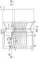
FIG. 7 shows semiconductor dies 12 a, 12 b of an assembly 10 c. The dies are configured so that they may be assembled in a face-to-face relationship analogous to that of FIG. 3. The bottom die 12 b is illustrated in a face-up orientation, and the top die 12 a is illustrated in a face-down orientation. Circuitry associated with the dies (e.g., redistribution wiring layers 15 a, 15 b; M3 pads 11 a, 11 b; etc.) is schematically illustrated as if viewed through all materials and structures that may be over the circuitry in order to simplify the drawings. However, it is to be understood that the circuitry may be covered with one or more materials; and, in the case of die 12 a, the circuitry is along a bottom of the die.
The die 12 a has coupling regions 30 a, 30 b, 30 c and 30 d; with the coupling regions 30 a, 30 b, 30 c and 30 d being laterally offset relative to one another. Analogously, the die 12 b has coupling regions 32 a, 32 b, 32 c and 32 d; with the coupling regions 32 a, 32 b, 32 c and 32 d being laterally offset relative to one another. When the dies are in face-to-face relationship, the coupling regions 30 a, 30 b, 30 c and 30 d align with the coupling regions 32 a, 32 b, 32 c and 32 d, respectively. Solder bumps or other suitable interconnects may be formed to interconnect coupling regions 30 a, 30 b, 30 c, 30 d with coupling regions 32 a, 32 b, 32 c, 32 d, as desired. In the shown embodiment, solder bumps 31 (or other suitable interconnects) are associated with regions 32 a and 32 b of die 12 b, and are utilized for bonding such regions to regions 30 a and 30 b, respectively, of die 12 a. Interconnects are not provided between the regions 30 c, 30 d and the regions 32 c, 32 d in the shown embodiment. The regions 30 a, 30 b, 30 c, 30 d, 32 a, 32 b, 32 c and 32 d may be referred to as landings, or in some specific embodiments as bump landings, to indicate that they are locations where bumps or other suitable coupling components interconnect with the redistribution wiring layers 15 a, 15 b.
The M3 pad regions (i.e. interconnection regions) 11 a are arranged in a first line 39 a extending along a face surface 14 of the first die 12 a (with the face surface 14 of the die 12 a being under the view of FIG. 7, but being shown in FIG. 8A); and the M3 pad regions 11 b are arranged in a second line 39 b extending along a face surface 14 of the second die 12 b. First redistribution wiring 18 a is electrically coupled with the M3 pad regions 11 a of the first die 12 a, and second redistribution wiring 18 b is electrically coupled with the M3 pad regions 11 b of the second die 12 b.
The first redistribution wiring 18 a is comprised by a first redistribution wiring layer 15 a, and the second redistribution wiring 18 b is comprised by a second redistribution wiring layer 15 b.
The first redistribution wiring layer 15 a has primary portions 36 extending outwardly from the M3 pad regions 11 a in a first lateral direction represented by an arrow 5, and has secondary portions 38 extending outwardly from the M3 pad regions 11 a in a second lateral direction represented by an arrow 7; with the second lateral direction represented by arrow 7 being opposite to the first lateral direction represented by arrow 5. The primary portions 36 include the coupling regions 30 c, 30 d and the wiring 18 a extending across such coupling regions; and the secondary portions 38 include the coupling regions 30 a, 30 b and the wiring 18 a extending across such coupling regions.
The second redistribution wiring layer 15 b has primary portions 40 extending outwardly from the M3 pad regions 11 b in the second lateral direction represented by the arrow 7, and has secondary portions 42 extending outwardly from the M3 pad regions 11 b in the first lateral direction represented by the arrow 5. The primary portions 40 include the coupling regions 32 a, 32 b and the wiring 18 b extending across such coupling regions; and the secondary portions 42 include the coupling regions 32 c, 32 d and the wiring 18 b extending across such coupling regions.
The terms “primary” and “secondary” are utilized to distinguish the portions of the first and second redistribution wiring layers 15 a, 15 b to assist in explaining the invention, and to assist in defining the invention in the claims which follow. In the illustrated embodiment of FIG. 7, the “primary” portions happen to be longer than the “secondary” portions. In other embodiments, portions analogous to the integrated “primary” portions may be shorter than portions analogous to the indicated “secondary” portions.
The coupling regions 32 a and 32 c are arranged symmetrically relative to the line 39 b of M3 pad regions 11 b in the embodiment of FIG. 7; with the coupling regions 32 a being laterally offset from the line 39 b by a distance x along the second direction represented by arrow 7, and the coupling regions 32 c being laterally offset from the line 39 b by the distance x along the first direction represented by arrow 5. Similarly, the coupling regions 32 b and 32 d are arranged symmetrically relative to the line 39 b of M3 pad regions 11 b in the embodiment of FIG. 7; with the coupling regions 32 b being laterally offset from the line 39 b by a distance y along the second direction represented by arrow 7, and the coupling regions 32 d being laterally offset from the line 39 b by the distance y along the first direction represented by arrow 5. The coupling regions 30 a and 30 c are also arranged symmetrically relative to the line 39 a of M3 pad regions 11 a, and similarly the coupling regions 30 b and 30 d are arranged symmetrically relative to the line 39 a.
An advantage of the embodiment of FIG. 7 is that the die 12 a may be substantially identical to the die 12 b (with “substantially identical” meaning identical to within reasonable tolerances of fabrication and measurement), and accordingly may be formed with identical processing as the die 12 b. Such may simplify fabrication, and reduce costs, as compared to other embodiments in which the dies 12 a and 12 b are not substantially identical to one another. In some embodiments, the first interconnection regions 11 a may be considered to be associated with the first redistribution wiring layer 15 a; with the first interconnection regions 11 a and the associated first redistribution wiring layer 15 a forming a first pattern 44 a. Similarly, the second interconnection regions 11 b may be considered to be associated with the second redistribution wiring layer 15 b; with the second interconnection regions 11 b and the associated second redistribution wiring layer 15 b forming a second pattern 44 b. In the embodiment of FIG. 7, the second pattern 44 b is substantially identical to the first pattern 44 a. In other embodiments, the second pattern may be different than the first pattern.
In the illustrated embodiment, the redistribution wiring layers 15 a of the top die 12 a extend to first pads 34 a, and the redistribution wiring layers 15 b of the bottom die 12 b extend to second pads 34 b. Such pads may be suitable for coupling with wires 19 of the type described above with reference to FIG. 3 and/or for coupling with a testing probe during testing of the dies 12 a, 12 b. In the shown embodiment, the pads 34 a and 34 b are illustrated to each comprise two regions (35 a, 37 a) and (35 b, 37 b); with the regions 35 a, 35 b being configured as “probe pads” (or in other words, being configured to be suitable for contact with a testing probe), and the regions 37 a, 37 b being configured as “bonding pads” (or in other words, being configured to be suitable for bonding to a wire 19 of the type shown above with reference to FIG. 3, or any other suitable interconnect). In other embodiments, the pads 34 a and 34 b may have other configurations. If the pads 34 a, 34 b have regions suitable for bonding with wires (e.g., 19 of FIG. 3), the bonding pads may be referred to as wire bonding pads.
In the illustrated embodiment, the first bonding pads 34 a are laterally offset from the first interconnecting regions 11 a along the first lateral direction represented by arrow 5, and the second bonding regions 34 b are laterally offset from the second interconnecting regions 11 b along the second lateral direction represented by arrow 7.
FIG. 8 shows assembly 10 c in an arrangement in which the dies are in face-to-face relationship. The bottom die 12 b is face up, and the top die 12 a is face down. The assembly 10 c is viewed downwardly through the backside surface 16 of the top die 12 a. Circuitry between the dies is schematically illustrated as if viewed through all materials and structures that may be over the circuitry. Overlap of the coupling regions 30 a, 30 b, 30 c and 30 d with the coupling regions 32 a, 32 b, 32 c and 32 d is apparent; as is the overlap of the M3 pad regions (i.e., interconnection regions) 11 a with the M3 pad regions (i.e., interconnection regions) 11 b. In the illustrated embodiment, the coupling regions 30 a are electrically coupled with the coupling regions 32 a through conductive interconnects (e.g., solder bumps) 31, and the coupling regions 30 b are electrically coupled with the coupling regions 32 b through conductive interconnects (e.g., solder bumps) 31. The coupling regions 30 d are vertically above the coupling regions 32 d but are not directly electrically coupled with such regions, and the coupling regions 30 c are vertically above the coupling regions 32 c but are not directly electrically coupled with such regions. Also, in the shown embodiment it may be that only the bonding regions 34 b are utilized for bonding to wires (or other suitable interconnects), and the bonding regions 34 a are simply vestigial; with the bonding regions 34 a having resulted from the desirability of forming die 12 a to be identical with die 12 b. Similarly, the coupling regions 30 c, 32 c, 30 d and 32 d may be vestigial. In other embodiments, the bonding regions 34 a may be utilized for coupling with circuitry, and accordingly may have a function instead of being simply vestigial structures with no apparent use in a final configuration. Similarly, one or more of the coupling regions 30 c, 32 c, 30 d and 32 d may be provided with a function instead of simply being a vestigial structure with no apparent use in the final configuration.
In the illustrated embodiment of FIG. 8, the bonding pads 37 a of the first die 12 a are overlapped by the second die 12 b, and the bonding pads 37 b of the second die 12 b are vertically overlapped by the first die 12 a. In other embodiments, it may be desired to have the bonding pads 37 a extending laterally outward beyond the die 12 b and/or to have the bonding pads 37 b extending laterally outward beyond the die 12 a, as discussed in more detail below with reference to FIGS. 16-19.
FIG. 8A shows a cross-section through assembly 10 c, and more clearly indicates that the first and second dies 12 a and 12 b are in face-to-face relationship with one another. One of the first interconnection regions 11 a can be seen to be vertically offset from one of the second interconnection regions 11 b (and directly over the second interconnection region 11 b in the shown embodiment). The secondary portion 38 of the first redistribution wiring layer 15 a is electrically coupled to the primary portion 40 of the second redistribution wiring layer 15 b through an interconnect 31 that couples one of the coupling regions 30 a with one of the coupling regions 32 a. The first interconnection region 11 a is electrically coupled to the wire 19 through a path 46 extends along the first redistribution wiring layer 15 a, through the interconnect 31, and along the second redistribution wiring layer 15 b to the wire bonding pad 34 b; and the second interconnection region 11 b electrically coupled to the same wire 19 through a path 48 that extends along the second redistribution wiring layer 15 b to the wire bonding pad 34 b. Accordingly, both of the interconnection regions 11 a and 11 b may be accessed utilizing the same wire 19 and the same wire bonding pad 34 b.
In some embodiments, it may be advantageous to utilize a die 12 a which is not identical to the die 12 b. For instance, the primary portions 36 of the redistribution wiring layer 15 a may be considered to comprise an open stub wiring 50 in the embodiment of FIG. 8A. Such open stub wiring may influence capacitance associated with the circuitry along die 12 a, which may adversely impact performance of such circuitry. Accordingly, it may be advantageous to reduce the overall size of the open stub wiring 50. FIGS. 9, 10 and 10A illustrate an assembly 10 d in which circuitry associated with the first die 12 a is different from that associated with the second die 12 b.
FIG. 9 shows semiconductor dies 12 a, 12 b configured so that they may be assembled in a face-to-face relationship. The die 12 b is illustrated in a face-up orientation, and the die 12 a is illustrated in a face-down orientation. Circuitry associated with the dies (e.g., redistribution wiring layers 15 a, 15 b; M3 pads 11 a, 11 b; etc.) is schematically illustrated as if viewed through all materials and structures that may be over the circuitry in order to simplify the drawings. However, it is to be understood that the circuitry may be covered with one or more materials; and, in the case of die 12 a, the circuitry is along a bottom of the die.
The dies 12 a and 12 b have the coupling regions 30 a and 32 a, respectively. When the dies are in face-to-face relationship, the coupling regions 30 a align with the coupling regions 32 a. Solder bumps or other suitable interconnects 31 may be formed to interconnect coupling regions 30 a with coupling regions 32 a.
The M3 pad regions (i.e. interconnection regions) 11 a are arranged in the first line 39 a, and the M3 pad regions 11 b are arranged in the second line 39 b. First redistribution wiring 18 a is electrically coupled with the M3 pad regions 11 a of the first die 12 a, and second redistribution wiring 18 b is electrically coupled with the M3 pad regions 11 b of the second die 12 b.
The first redistribution wiring 18 a is comprised by a first redistribution wiring layer 15 a, and the second redistribution wiring 18 b is comprised by a second redistribution wiring layer 15 b.
The first redistribution wiring layer 15 a has the primary portions 36 extending outwardly from the M3 pad regions 11 a in the first lateral direction represented by the arrow 5, and has the secondary portions 38 extending outwardly from the M3 pad regions 11 a in the second lateral direction represented by the arrow 7. The second redistribution wiring layer 15 b has the primary portions 40 extending outwardly from the M3 pad regions 11 b in the second lateral direction represented by the arrow 7, and has the secondary portions 42 extending outwardly from the M3 pad regions 11 b in the first lateral direction represented by the arrow 5.
In the embodiment of FIG. 9, the probe pads 35 a, 35 b are separated from bonding pads (37 a, 37 b of FIG. 7). Only one set of bonding pads is utilized in FIG. 9, and such bonding pads are simply labeled 37. The bonding pads 37 are only along the bottom die 12 b, rather than being along both of the dies 12 a and 12 b like the embodiment of FIG. 7. The probe pads 35 a are arranged in a line 52 a along the face of the first die 12 a, and the probe pads 35 b are arranged in an analogous line 52 b along the face of the second die 12 b. The probe pads 35 a are laterally spaced from the first interconnection regions 11 a by a distance z along the first lateral direction represented by the arrow 5, and the probe pads 35 b are spaced from the second interconnection regions 11 b by the same distance z along the second lateral direction represented by the arrow 7. Accordingly, substantially identical capacitance may be encountered in testing interconnecting regions 11 a of die 12 a with probe pads 35 a as is encountered in testing interconnecting regions 11 b of die 12 b with probe pads 35 b; and thus, the same testing tool may be utilized for testing both dies.
The die 12 a is not substantially identical to the die 12 b in the embodiment of FIG. 9 (for instance, the primary region 36 of the redistribution wiring layer 15 a is shorter than the primary region 40 of the redistribution wiring layer 15 b), but advantages achieved with the particular configurations of dies 12 a and 12 b (e.g., advantages in being able to use the same testing probe for both dies) may offset disadvantages associated with the need to separately fabricate each of the dies. Notably, even though the redistribution wiring of dies 12 a and 12 b is different (wiring 15 a has a different configuration than wiring 15 b), the probe pads 35 a and 35 b are arranged in the same positions as one another.
FIG. 10 shows assembly 10 d in an arrangement in which the dies are in face-to-face relationship. The bottom die 12 b is face up, and the top die 12 a is face down. The assembly 10 d is viewed downwardly through the backside surface 16 of the top die 12 a. Circuitry between the dies is schematically illustrated as if viewed through all materials and structures that may be over the circuitry. Overlap of the coupling regions 30 a with the coupling regions 32 a is apparent; as is the overlap of the M3 pad regions (i.e., interconnection regions) 11 a and 11 b.
FIG. 10A shows a cross-section through assembly 10 d, and more clearly indicates that the first and second dies 12 a and 12 b are in face-to-face relationship with one another. One of the first interconnection regions 11 a can be seen to be vertically offset from one of the second interconnection regions 11 b (and is directly over the second interconnection region 11 b in the shown embodiment). The first and second interconnection regions 11 a and 11 b are electrically coupled to the wire 19 through the paths 46 and 48 of the types described above with reference to FIG. 8A. The assembly 10 d of FIG. 10A may be advantageous relative to the assembly 10 c of FIG. 8A in some applications, in that the open stub 50 of assembly 10 d is shorter than that of assembly 10 c; and the probe pads 35 a, 35 b are closer to the M3 pads 11 a, 11 b in assembly 10 d while remaining equidistant from the M3 pads relative to one another.
FIGS. 11, 12, 12A and 12B illustrate an assembly 10 e in which circuitry associated with the first die 12 a is the same as that associated with the second die 12 b (or at least substantially identical to that of the second die 12 b); and yet in which the redistribution wiring path from an interconnection region 11 a may comprise a unique (i.e., not shared) bonding pad/probe pad, and the redistribution wiring path from an interconnection region 11 b may comprise a unique bonding pad/probe pad.
FIG. 11 shows semiconductor dies 12 a, 12 b configured so that they may be assembled in a face-to-face relationship. The die 12 b is illustrated in a face-up orientation, and the die 12 a is illustrated in a face-down orientation. Circuitry associated with the dies (e.g., redistribution wiring layers 15 a, 15 b; M3 pads 11 a, 11 b; etc.) is schematically illustrated as if viewed through all materials and structures that may be over the circuitry in order to simplify the drawings. However, it is to be understood that the circuitry may be covered with one or more materials; and, in the case of die 12 a, the circuitry is along a bottom of the die.
The dies 12 a and 12 b of FIG. 11 are similar to the dies 12 a and 12 b of FIG. 7; and have the redistribution wiring 18 a, 18 b; coupling regions 30 a, 30 b, 30 c, 30 d, 32 a, 32 b, 32 c, 32 d; and pads 11 a, 11 b within redistribution wiring layers 15 a, 15 b. The dies 12 a and 12 of FIG. 11 differ from those of FIG. 7 in that the dies 12 a and 12 b of FIG. 11 comprise wiring trace regions (i.e., control regions, or tailored regions) 51 a and 51 b, respectively; which are configured to enable an upper pad 11 a to be accessed through a probe location which is not shared with a lower pad 11 b during a control pulse; and which also enable a lower pad 11 b to be accessed through a probe location which is not shared an upper pad 11 a.
The region 51 a comprises a wiring segment 54 a which extends to one of the interconnection regions 11 a, and comprises another wiring segment 54 b which is physically separate from the wiring segment 54 a and which does not extend to any of the interconnection regions 11 a. Both of the wiring segments 54 a and 54 b may be comprised by the redistribution wiring layer 15 a, and may be considered to be portions of the redistribution wiring 18 a. The region 51 b comprises a wiring segment 56 a which extends to one of the interconnection regions 11 b, and comprises another wiring segment 56 b which is physically separate from the wiring segment 56 a and which does not extend to any of the interconnection regions 11 b. Both of the wiring segments 56 a and 56 b may be comprised by the redistribution wiring layer 15 b, and may be considered to be portions of the redistribution wiring 18 b.
In some embodiments, the segments 54 a, 56 a, 56 b and 54 b may be referred to as first, second, third and fourth wiring segments, respectively. The third wiring segment 56 b is electrically coupled to the first wiring segment 54 a through a bonding region 58; with the bonding region 58 including a coupling region 30 b, a coupling region 32 b, and an interconnect 31.
FIG. 12 shows assembly 10 e in an arrangement in which the dies are in face-to-face relationship. The bottom die 12 b is face up, and the top die 12 a is face down. The assembly 10 e is viewed downwardly through the backside surface 16 of the top die 12 a. Circuitry between the dies is schematically illustrated as if viewed through all materials and structures that may be over the circuitry.
FIG. 12A shows a cross-section through assembly 10 e along the wiring segments 54 a, 56 b; and FIG. 12B shows a cross-section through assembly 10 e along the wiring segments 54 b, 56 a.
Electrical coupling of the first and third wiring segments 54 a, 56 b through the bonding region 58 is apparent in FIGS. 12 and 12A.
FIGS. 12, 12A and 12B show that the bonding pad/probe pad electrically coupled with the wiring trace formed from combined wiring segments 54 a, 56 b (labeled 60 in FIGS. 12, 12A and 12B to distinguish it from other bonding pad/probe pads) is different from the bonding pad/probe pad electrically coupled with wiring segment 58 (labeled 62 in FIGS. 12, 12A and 12B to distinguish it from other bonding pad/probe pads).
An interconnection region 11 a within wiring trace region 51 a/51 b may be uniquely accessed through pad 60, and an interconnection region 11 b within the wiring trace region 51 a/51 b may be uniquely accessed through pad 62.
The first interconnection region 11 a of FIG. 12A is electrically coupled to a wire 19 through a path 64 that extends along wiring segments 56 b and 54 a, and through pad 60; and the second interconnection region 11 b of FIG. 12B is electrically coupled to a wire 19 through a path 66 that extends along wiring segment 56 a and through pad 62.
FIGS. 11, 12, 12A and 12B illustrate an embodiment in which the first and second dies 12 a, 12 b are substantially identical to one another. In some embodiments, it may be advantageous to utilize a die 12 a which is not identical to the die 12 b (as discussed above with reference to FIGS. 9, 10 and 10A). FIGS. 13, 14, 14A and 14B illustrate an assembly 10 f similar to the assembly 10 e of FIGS. 11, 12, 12A and 12B, but in which circuitry associated with the first die 12 a is different from that associated with the second die 12 b.
FIG. 13 shows semiconductor dies 12 a, 12 b configured so that they may be assembled in a face-to-face relationship. The die 12 b is illustrated in a face-up orientation, and the die 12 a is illustrated in a face-down orientation. Circuitry associated with the dies (e.g., redistribution wiring layers 15 a, 15 b; M3 pads 11 a, 11 b; etc.) is schematically illustrated as if viewed through all materials and structures that may be over the circuitry in order to simplify the drawings. However, it is to be understood that the circuitry may be covered with one or more materials; and, in the case of die 12 a, the circuitry is along a bottom of the die.
The dies 12 a and 12 b of FIG. 13 are similar to the dies 12 a and 12 b of FIG. 9, but also include wiring trace region (i.e., control regions, or tailored regions) 51 a and 51 b, respectively, similar to those described with reference to FIG. 11. The dies 12 a and 12 b of FIG. 13 have the redistribution wiring 18 a, 18 b; coupling regions 30 a, 32 a; and pads 11 a, 11 b within redistribution wiring layers 15 a, 15 b. The dies 12 a and 12 of FIG. 13 comprise wiring segments 54 a, 56 a and 56 b within the regions 51 a and 51 b. Notably, there is no wiring segment 54 b of the type shown in FIG. 11.
In some embodiments, the segments 54 a, 56 a and 56 b may be referred to as first, second and third wiring segments, respectively. The third wiring segment 56 b is electrically coupled to the first wiring segment 54 a through a bonding region 58; with the bonding region 58 including a coupling region 68 along wiring segment 54 a, a coupling region 70 along wiring segment 56 b, and an interconnect 31.
FIG. 14 shows assembly 10 f in an arrangement in which the dies are in face-to-face relationship. The bottom die 12 b is face up, and the top die 12 a is face down. The assembly 10 f is viewed downwardly through the backside surface 16 of the top die 12 a. Circuitry between the dies is schematically illustrated as if viewed through all materials and structures that may be over the circuitry. Electrical coupling of the first and third wiring segments 54 a, 56 b through the bonding region 58 is apparent. FIG. 14 also shows a bonding pad 60 electrically coupled with the wiring trace formed from combined wiring segments 54 a, 56 b; and a bonding pad 62 electrically coupled with wiring segment 58. It is noted that the pads 60, 62 of the embodiment of FIG. 12 included both probe pad regions 35 and bonding pad regions 37; whereas the pads 60, 62 of FIG. 14 comprise only bonding pad regions as the probe pad regions 35 are separated from the bonding pad regions 37 in a manner similar to the embodiment of FIG. 10 (discussed above).
FIG. 14A shows a cross-section through assembly 10 f along the wiring segments 54 a, 56 b; and FIG. 14B shows a cross-section through assembly 10 f along the wiring segments 54 a, 56 a. The first interconnection region 11 a of FIG. 14A is electrically coupled to a wire 19 through a path 64 that extends along wiring segments 56 b and 54 a, and through pad 60; and the second interconnection region 11 b of FIG. 14B is electrically coupled to a wire 19 through a path 66 that extends along wiring segment 56 a and through pad 62.
The paired dies 12 a, 12 b of the above-described embodiments may be considered together to form a first face-to-face die assembly. In some embodiments, a packaged assembly may be fabricated to comprise multiple face-to-face die assemblies. For instance, FIG. 15 shows a packaged assembly 10 g in which the dies 12 a, 12 b form a first face-to-face die assembly 72 a, and in which a second pair of dies 12 c, 12 d form a second face-to-face die assembly 72 b. The second face-to-face die assembly 72 b is vertically disposed relative to the first face-to-face die assembly 72 a. Although two face-to- face die assemblies 72 a, 72 b are illustrated, in other embodiments analogous packages may comprise more than two face-to-face die assemblies.
In the shown embodiment, the assemblies 72 a and 72 b are vertically separated from one another by an intervening insulative region 74. The insulative region 74 may comprise any suitable composition or combination of compositions, such as, for example, one or more of silicon dioxide, silicon nitride, etc.
Each of the die assemblies 72 a, 72 b has a bonding pad 37 coupled with a wire (or any other suitable connection) 19. The wires 19 extend to a common region of the substrate 20 comprising circuitry suitable for accessing redistribution layers along the die assemblies 72 a, 72 b. In some embodiments, the face-to-face die assembly 72 b may be substantially identical to the face-to-face die assembly 72 a. Accordingly, each redistribution layer of the second die assembly 72 b may have a corresponding redistribution layer of the first die assembly 72 a. The cross-section of FIG. 15 be considered to show a redistribution layer 15 of the first assembly 72 a, and a corresponding redistribution layer 15 of the second assembly 72 b.
The redistribution layer 15 of assembly 72 a and the corresponding redistribution layer 15 of assembly 72 b may be coupled through the wires 19 to a same region of circuitry associated with substrate 20; and other corresponding redistribution layers of the assemblies 72 a, 72 b may similarly be coupled with common circuitry as one another along the substrate 20. Accordingly, control circuitry along substrate 20 may be shared by the vertically stacked assemblies 72 a, 72 b which may advantageously reduce production costs. Further, utilization of stacked assemblies 72 a, 72 b which are substantially identical to one another may enable common masks and processing steps to be utilized for fabricating each of the stacked assemblies, which may reduce production costs as compared to processes utilizing stacked assemblies which differ from one another. Also, common testing may be utilized for assembly 72 b as is utilized for assembly 72 a in embodiments in which the assemblies are substantially identical to one another, which may enable a common testing probe to be utilized for testing of all of the dies 12 a, 12 b, 12 c, 12 d; which may reduce costs as compared to embodiments in which multiple different testing probe configurations are needed.
The assemblies 72 a, 72 b of FIG. 15 are shown comprising bonding pads 37. In some embodiments, the assemblies may also comprise bonding pads 60, 62 of the type described above with reference to embodiments of FIGS. 11-14 as being associated with control traces.
The assemblies discussed above have the lower dies 12 b aligned with the upper dies 12 a; and have bond pads 37, 60 and 62 of the lower die 12 b (i.e., second chip) overlapped by the upper die (i.e., first chip). In other embodiments, analogous assemblies may be configured such that upper dies 12 a are laterally shifted relative to the lower dies 12 b; and in some embodiments, the bond pads of the lower die 12 b of a face-to-face die assembly extend laterally outward beyond the upper die 12 a to simplify bonding of wires or other suitable interconnects to the bond pads 12 a. Additionally, or alternatively, the bond pads of the upper die 12 a may extend laterally outward beyond the lower die 12 b. FIGS. 16-27 show example assemblies in which upper dies are laterally offset relative to lower dies; and illustrate embodiments in which bond pads of at least one of the paired face-to-face dies extend laterally outward of the other die.
Referring to 16, 17 and 17A, such show semiconductor dies 12 a, 12 b configured so that they may be assembled in a face-to-face relationship in an assembly 10 h. The die 12 b is illustrated in a face-up orientation, and the die 12 a is illustrated in a face-down orientation. Circuitry associated with the dies (e.g., redistribution wiring layers 15 a, 15 b; M3 pads 11 a, 11 b; etc.) is schematically illustrated as if viewed through all materials and structures that may be over the circuitry in order to simplify the drawings. However, it is to be understood that the circuitry may be covered with one or more materials; and, in the case of die 12 a, the circuitry is along a bottom of the die.
The dies 12 a and die 12 b have the coupling regions 30 and 32, respectively. When the dies are in face-to-face relationship, the coupling regions 30 align with the coupling regions 32. Solder bumps or other suitable interconnects 31 may be formed to interconnect coupling regions 30 with coupling regions 32.
The M3 pad regions (i.e. interconnection regions) 11 a are arranged in the first line 39 a, and the M3 pad regions 11 b are arranged in the second line 39 b. First redistribution wiring 18 a is electrically coupled with the M3 pad regions 11 a of the first die 12 a, and second redistribution wiring 18 b is electrically coupled with the M3 pad regions 11 b of the second die 12 b.
The coupling regions 32 are laterally offset from the line 39 b by a distance “a/2” along the first direction represented by the arrow 5, and the coupling regions 30 are laterally offset from the line 39 a by the distance “a/2” along the second direction represented by the arrow 7.
The first redistribution wiring 18 a is comprised by the first redistribution wiring layer 15 a, and the second redistribution wiring 18 b is comprised by the second redistribution wiring layer 15 b.
The first redistribution wiring layer 15 a has the primary portions 36 extending outwardly from the M3 pad regions 11 a in the first lateral direction represented by the arrow 5, and has the secondary portions 38 extending outwardly from the M3 pad regions 11 a in the second lateral direction represented by the arrow 7. The second redistribution wiring layer 15 b has the primary portions 40 extending outwardly from the M3 pad regions 11 b in the second lateral direction represented by the arrow 7, and has the secondary portions 42 extending outwardly from the M3 pad regions 11 b in the first lateral direction represented by the arrow 5.
The redistribution wiring layers 15 a of the top die 12 a extend to first pads 34 a, and the redistribution wiring layers 15 b of the bottom die 12 b extend to second pads 34 b. The pads 34 a and 34 b comprise regions 35 a, 37 a, 35 b and 37 b; with the regions 35 a, 35 b being the probe pads, and the regions 37 a, 37 b being the bonding pads.
The dies 12 a and 12 b are substantially identical to one another.
FIG. 17 shows assembly 10 h in an arrangement in which the dies are in face-to-face relationship. The bottom die 12 b is face up, and the top die 12 a is face down. The assembly 10 h is viewed downwardly through the backside surface 16 of the top die 12 a. Circuitry between the dies is schematically illustrated as if viewed through all materials and structures that may be over the circuitry. Overlap of the coupling regions 30 with the coupling regions 32 is apparent; as is lateral spacing of the M3 pad regions (i.e., interconnection regions) 11 a and 11 b by a distance “a”.
FIG. 17A shows a cross-section through assembly 10 h, and more clearly indicates that the first and second dies 12 a and 12 b are in face-to-face relationship with one another. One of the first interconnection regions 11 a can be seen to be both vertically displaced and laterally offset from one of the second interconnection regions 11 b. The first interconnection region 11 a is electrically coupled to the wire 19 through a path along wiring 18 a and 18 b, and the second interconnection region 11 b is electrically coupled to the wire 19 through a path along wiring 18 b. The assembly 10 h of FIG. 17A advantageously has bond pad 34 b uncovered by the upper die 12 a which can simplify bonding of the wire 19 to bond pad 34 b, and which removes some limitations on the profile of the wire bonding as compared to embodiments in which bond pads 34 b are covered by the upper die 12 a.
Referring to 18, 19 and 19A, such show semiconductor dies 12 a, 12 b configured so that they may be assembled in a face-to-face relationship in an assembly 10 i having wiring trace regions (i.e., control regions, or tailored regions) 51 a and 51 b, respectively analogous to the those discussed above with reference to FIGS. 11, 12 and 12A. The die 12 b is illustrated in a face-up orientation, and the die 12 a is illustrated in a face-down orientation. Circuitry associated with the dies (e.g., redistribution wiring layers 15 a, 15 b; M3 pads 11 a, 11 b; etc.) is schematically illustrated as if viewed through all materials and structures that may be over the circuitry in order to simplify the drawings. However, it is to be understood that the circuitry may be covered with one or more materials; and, in the case of die 12 a, the circuitry is along a bottom of the die.
The die 12 a has the coupling regions 30 (specifically, 30 a, 30 b and 30 c), and the die 12 b has the coupling regions 32 (specifically, 32 a, 32 b and 32 c). When the dies are in face-to-face relationship, the coupling regions 30 align with the coupling regions 32. Solder bumps or other suitable interconnects 31 may be formed to interconnect coupling regions 30 a, 30 b with coupling regions 32 a, 32 b.
First redistribution wiring 18 a is electrically coupled with the M3 pad regions 11 a of the first die 12 a, and second redistribution wiring 18 b is electrically coupled with the M3 pad regions 11 b of the second die 12 b. The first redistribution wiring 18 a is comprised by the first redistribution wiring layer 15 a, and the second redistribution wiring 18 b is comprised by the second redistribution wiring layer 15 b.
The dies 12 a and 12 b are substantially identical to one another.
FIG. 19 shows assembly 10 i in an arrangement in which the dies are in face-to-face relationship. The bottom die 12 b is face up, and the top die 12 a is face down. The assembly 10 i is viewed downwardly through the backside surface 16 of the top die 12 a. Circuitry between the dies is schematically illustrated as if viewed through all materials and structures that may be over the circuitry. Overlap of the coupling regions 30 a, 30 b and 30 c with the coupling regions 32 a, 32 b and 32 c is apparent; as is lateral spacing of the M3 pad regions (i.e., interconnection regions) 11 a and 11 b by the distance “a”.
FIG. 19A shows a cross-section through assembly 10 i along the wiring segments 54 a, 56 b; and FIG. 19B shows a cross-section through assembly 10 i along the wiring segments 54 b, 56 a. The first interconnection region 11 a of FIG. 19A is electrically coupled to a wire 19 through a path 64 that extends along wiring segments 56 b and 54 a, and through pad 60; and the second interconnection region 11 b of FIG. 19B is electrically coupled to a wire 19 through a path 66 that extends along wiring segment 56 a and through pad 62.
The wire bonding pads and probe pads (analogous to the pads 37, 35 discussed above) may be placed in any suitable locations within the illustrated pads 34 a, 34 b, 60 and 62 of the assembly 10 i of FIGS. 18, 19 and 19A.
Referring to FIG. 20, such shows semiconductor dies 12 a, 12 b configured so that they may be assembled in a face-to-face relationship in an assembly 10 j. The die 12 b is illustrated in a face-up orientation, and the die 12 a is illustrated in a face-down orientation. Circuitry associated with the dies (e.g., redistribution wiring layers 15 a, 15 b; M3 pads 11 a, 11 b; etc.) is schematically illustrated as if viewed through all materials and structures that may be over the circuitry in order to simplify the drawings. However, it is to be understood that the circuitry may be covered with one or more materials; and, in the case of die 12 a, the circuitry is along a bottom of the die.
The dies 12 a and die 12 b have the coupling regions 30 and 32, respectively. When the dies are in face-to-face relationship, the coupling regions 30 align with the coupling regions 32. Solder bumps or other suitable interconnects 31 may be formed to interconnect coupling regions 30 with coupling regions 32.
The M3 pad regions (i.e. interconnection regions) 11 a are arranged in the first line 39 a, and the M3 pad regions 11 b are arranged in the second line 39 b. First redistribution wiring 18 a is electrically coupled with the M3 pad regions 11 a of the first die 12 a, and second redistribution wiring 18 b is electrically coupled with the M3 pad regions 11 b of the second die 12 b.
The coupling regions 32 are laterally offset from the line 39 b by a distance “a/2” along the second direction represented by the arrow 7, and the coupling regions 30 are laterally offset from the line 39 a by the distance “a/2” along the first direction represented by the arrow 5.
The first redistribution wiring 18 a is comprised by the first redistribution wiring layer 15 a, and the second redistribution wiring 18 b is comprised by the second redistribution wiring layer 15 b.
The redistribution wiring layers 15 a of the top die 12 a extend to first pads 34 a, and the redistribution wiring layers 15 b of the bottom die 12 b extend to second pads 34 b. The pads 34 a and 34 b comprise regions 35 a, 37 a, 35 b and 37 b; with the regions 35 a, 35 b being the probe pads, and the regions 37 a, 37 b being the bonding pads.
The dies 12 a, 12 b are substantially identical to one another.
FIG. 21 shows assembly 10 j in an arrangement in which the dies are in face-to-face relationship. The bottom die 12 b is face up, and the top die 12 a is face down. The assembly 10 h is viewed downwardly through the backside surface 16 of the top die 12 a. Circuitry between the dies is schematically illustrated as if viewed through all materials and structures that may be over the circuitry. Overlap of the coupling regions 30 with the coupling regions 32 is apparent; as is lateral spacing of the M3 pad regions (i.e., interconnection regions) 11 a and 11 b by a distance “a”.
FIG. 21A shows a cross-section through assembly 10 i, and more clearly indicates that the first and second dies 12 a and 12 b are in face-to-face relationship with one another. One of the first interconnection regions 11 a can be seen to be both vertically displaced and laterally offset from one of the second interconnection regions 11 b. The first interconnection region 11 a is electrically coupled to a wire 19 through a path along wiring 18 a and 18 b, and the second interconnection region 11 b is electrically coupled to the wire 19 through a path along wiring 18 b. The assembly 10 i of FIG. 21A has bond pad 34 b offset relative to an edge of the upper die 12 a.
Referring to 22, 23, 23A and 23B, such show semiconductor dies 12 a, 12 b configured so that they may be assembled in a face-to-face relationship in an assembly 10 k having wiring trace regions (i.e., control regions, or tailored regions) 51 a and 51 b, respectively analogous to the those discussed above with reference to FIGS. 18, 19 and 19A. The die 12 b is illustrated in a face-up orientation, and the die 12 a is illustrated in a face-down orientation. Circuitry associated with the dies (e.g., redistribution wiring layers 15 a, 15 b; M3 pads 11 a, 11 b; etc.) is schematically illustrated as if viewed through all materials and structures that may be over the circuitry in order to simplify the drawings. However, it is to be understood that the circuitry may be covered with one or more materials; and, in the case of die 12 a, the circuitry is along a bottom of the die.
The die 12 a has the coupling regions 30 (specifically, 30 a, 30 b and 30 c), and the die 12 b has the coupling regions 32 (specifically, 32 a, 32 b and 32 c). When the dies are in face-to-face relationship, the coupling regions 30 align with the coupling regions 32. Solder bumps or other suitable interconnects 31 may be formed to interconnect coupling regions 30 a and 30 b with coupling regions 32 a and 32 b.
First redistribution wiring 18 a is electrically coupled with the M3 pad regions 11 a of the first die 12 a, and second redistribution wiring 18 b is electrically coupled with the M3 pad regions 11 b of the second die 12 b.
The first redistribution wiring 18 a is comprised by a first redistribution wiring layer 15 a, and the second redistribution wiring 18 b is comprised by a second redistribution wiring layer 15 b.
The dies 12 a, 12 b are substantially identical to one another.
FIG. 23 shows assembly 10 k in an arrangement in which the dies are in face-to-face relationship. The bottom die 12 b is face up, and the top die 12 a is face down. The assembly 10 k is viewed downwardly through the backside surface 16 of the top die 12 a. Circuitry between the dies is schematically illustrated as if viewed through all materials and structures that may be over the circuitry. Overlap of the coupling regions 30 with the coupling regions 32 is apparent; as is lateral offset of the M3 pad regions (i.e., interconnection regions) 11 a and 11 b. Also, the dies 12 a and 12 b are laterally offset relative to one another.
FIG. 23A shows a cross-section through assembly 10 k along the wiring segments 54 a, 56 b; and FIG. 23B shows a cross-section through assembly 10 k along the wiring segments 54 b, 56 a. The first interconnection region 11 a of FIG. 23A is electrically coupled to a wire 19 through a path 64 that extends along wiring segments 56 b and 54 a, and through pad 60; and the second interconnection region 11 b of FIG. 23B is electrically coupled to a wire 19 through a path 66 that extends along wiring segment 56 a and through pad 62.
The wire bonding pads and probe pads may be placed in any suitable locations within the illustrated pads 34 a, 34 b, 60 and 62 of the assembly 10 k of FIGS. 22, 23, 23A and 23B.
The embodiments of FIGS. 16-23 may be considered to laterally slip the dies 12 a, 12 b relative to one another. This may provide advantages relative to embodiments in which the dies are not laterally slipped relative to one another (for instance, the embodiment of FIGS. 11-12) in that the number of bump lands may be reduced by half.
The paired dies 12 a, 12 b of the embodiments of FIGS. 16-23 may be incorporated into packaged assemblies having multiple face-to-face assemblies (e.g., assemblies analogous to the assembly 10 g discussed above with reference to FIG. 15). For instance, FIGS. 24 and 25 shows packaged assemblies 10 l and 10 m, respectively, in which the dies 12 a, 12 b form a first face-to-face die assembly 72 a, and in which a second pair of dies 12 c, 12 d form a second face-to-face die assembly 72 b. The packaged assembly 10 l of FIG. 24 comprise face-to-face dies in the configuration described above with reference to FIGS. 16, 17 and 17A; and the packaged assembly 10 m of FIG. 25 comprise face-to-face dies in the configuration described above with reference to FIGS. 20, 21 and 21A.
In some embodiments, one of the first interconnection regions 11 a may be utilized in a supply circuit together with one of the second interconnection regions 11 b. FIGS. 26-36 illustrate example embodiments of supply circuits configured to utilize a pair of regions 11 a and 11 b.
Referring to FIG. 26, such shows semiconductor dies 12 a, 12 b configured so that they may be assembled in a face-to-face relationship in an assembly 10 n. The die 12 b is illustrated in a face-up orientation, and the die 12 a is illustrated in a face-down orientation. Circuitry associated with the dies (e.g., redistribution wiring layers 15 a, 15 b; M3 pads 11 a, 11 b; etc.) is schematically illustrated as if viewed through all materials and structures that may be over the circuitry in order to simplify the drawings. However, it is to be understood that the circuitry may be covered with one or more materials; and, in the case of die 12 a, the circuitry is along a bottom of the die.
The dies 12 a and die 12 b have the coupling regions 30 a, 30 b, 32 a and 32 b. When the dies are in face-to-face relationship, the coupling regions 30 a align with the coupling regions 32 a, and the coupling regions 30 b align with the coupling regions 32 b. Solder bumps or other suitable interconnects 31 may be formed to interconnect coupling regions 30 a with coupling regions 32 a, and to interconnect the coupling regions 30 b with coupling regions 32 b.
The M3 pad regions (i.e. interconnection regions) 11 a are arranged in the first line 39 a, and the M3 pad regions 11 b are arranged in the second line 39 b. First redistribution wiring 18 a is electrically coupled with the M3 pad regions 11 a of the first die 12 a, and second redistribution wiring 18 b is electrically coupled with the M3 pad regions 11 b of the second die 12 b.
A supply circuit 80 comprises a region 78 a along first die 12 a, and a region 78 b along second die 12 b. The region 78 a of the supply circuit 80 comprises one of the first interconnection regions labeled as 11 c, and the region 78 b of the supply circuit 80 comprises one of the second interconnection regions labeled as 11 d. The interconnection region 11 c is along a first wiring 82 a extending between coupling regions 84 a and 84 b, with the wiring 82 a being along the first die 12 a. The interconnection region 11 d is along a wiring 82 b extending between coupling regions 86 c and 86 d, with the wiring 82 b being along the second die 12 b. In some embodiments, one of the wirings 82 a, 82 b may be referred to as a first wiring and the other may be referred to as a second wiring.
The region 78 a also comprises coupling regions 84 c and 84 d which align with the regions 86 c and 86 d of region 78 b; and the region 78 b also comprises coupling regions 86 a and 86 b which align with the regions 84 a and 84 b of region 78 a. The regions 86 a and 86 b are within a VDD plane and VSS plane, respectively (i.e., are coupled with VDD circuitry and VSS circuitry, respectively); and the regions 84 c and 84 d are coupled with the VSS and VDD circuitry, respectively.
The redistribution wiring layers 15 a of the top die 12 a extend to first pads 34 a, and the redistribution wiring layers 15 b of the bottom die 12 b extend to second pads 34 b. The pads 34 a and 34 b comprise regions 35 a, 37 a, 35 b and 37 b; with the regions 35 a, 35 b being the probe pads, and the regions 37 a, 37 b being the bonding pads. The supply circuit regions 78 a and 78 b include pads 88, 90, 92 and 94.
FIG. 27 shows assembly 10 n in an arrangement in which the dies are in face-to-face relationship, and in which the supply circuit 80 provides VDD. The bottom die 12 b is face up, and the top die 12 a is face down. The assembly 10 n is viewed downwardly through the backside surface 16 of the top die 12 a. Circuitry between the dies is schematically illustrated as if viewed through all materials and structures that may be over the circuitry. Overlap of the coupling regions 30 a/32 a and 30 b/32 b is apparent; as is vertical overlap of the interconnection regions 11 a and 11 b. Additionally, it can be seen that there is overlap of coupling regions 84 a/86 a, 84 b/86/b, 84 c/86 c and 84 d/86 d; as well as vertical overlap of interconnection regions 11 c/11 d. Regions 84 a/86 a are electrically coupled to one another through an interconnect 31, and regions 84 d/86 d are also electrically coupled to one another through an interconnect 31. The regions 84 b/86 b are not electrically coupled with one another, and the regions 84 c/86 c are also not electrically coupled with one another.
FIG. 28 shows assembly 10 n in an arrangement analogous to that of FIG. 27, but in which the supply circuit 80 provides VSS. Regions 84 b/86 b are electrically coupled to one another through an interconnect 31, and regions 84 c/86 c are also electrically coupled to one another through an interconnect 31. The regions 84 a/86 a are not electrically coupled with one another, and the regions 84 d/86 d are also not electrically coupled with one another.
It is noted that there is substantial mirror symmetry across a horizontal plane along the supply region 80 of FIGS. 27 and 28, as indicated with the common distance “b” from the center of the supply region 80 to the middle of pads 88, 90, 92 and 94.
FIG. 27A shows a cross-section through assembly 10 n along the line 27A-27A of FIG. 27; and FIG. 28A shows a cross-section through assembly 10 n along the line 28A-28A of FIG. 28. The VDD supply of FIG. 27A includes a path 96 that extends along the second lateral direction represented by arrow 7, and a path 98 that extends along the first lateral direction represented by arrow 5. The path 96 extends from the first interconnect region 11 c, through a region of the wiring 82 a along the first die 12 a, through the electrically connected coupling regions 84 a/86 a, through a region of the wiring 82 b along the second die 12 b, and to a wire 19 electrically coupled with VDD. In some embodiments, the path 96 may being considered to comprise a first wiring segment 100 extending from interconnect 11 c to coupling region 84 a, and a second wiring segment 102 extending from coupling region 86 a to pad 92. Notably, the second wiring segment 102 is offset from the second interconnect region 11 d along the second lateral direction represented by arrow 7 in the cross-sectional view of FIG. 27A. The path 98 extends from the second interconnect region 11 d, through a region of the wiring segment 82 b along the second die 12 b and through the electrically coupled regions 84 d/86 d. In some embodiments, the path 98 may be considered to comprise a third wiring segment 104 which extends from the interconnect region 11 d to the coupling region 86 d.
The VSS supply of FIG. 28A includes a path 106 that extends along the second lateral direction represented by arrow 7, and a path 108 that extends along the first lateral direction represented by arrow 5. The path 108 extends from the first interconnect region 11 c, through a region of the wiring 82 a along the first die 12 a, through the electrically connected coupling regions 84 b/86 b, through a region of the wiring 82 b along the second die 12 b, and to a wire 19 electrically coupled with VSS. In some embodiments, the path 108 may being considered to comprise a first wiring segment 110 extending from interconnect 11 c to coupling region 84 b, and a second wiring segment 112 extending from coupling region 86 b to pad 94. Notably, the second wiring segment 112 is offset from the second interconnect region 11 d along the first lateral direction represented by arrow 5 in the cross-sectional view of FIG. 27A. The path 106 extends from the second interconnect region 11 d, through a region of the wiring segment 82 b along the second die 12 b and through the electrically coupled regions 84 c/86 c. In some embodiments, the path 106 may be considered to comprise a third wiring segment 114 which extends from the interconnect region 11 d to the coupling region 86 c.
Referring to FIG. 29, such shows semiconductor dies 12 a, 12 b configured so that they may be assembled in a face-to-face relationship in an assembly 10 o. The die 12 b is illustrated in a face-up orientation, and the die 12 a is illustrated in a face-down orientation. Circuitry associated with the dies (e.g., redistribution wiring layers 15 a, 15 b; M3 pads 11 a, 11 b; etc.) is schematically illustrated as if viewed through all materials and structures that may be over the circuitry in order to simplify the drawings. However, it is to be understood that the circuitry may be covered with one or more materials; and, in the case of die 12 a, the circuitry is along a bottom of the die.
The die 12 a has the coupling regions 30 a, 30 b, 30 c, 30 d; and the die 12 b has the coupling regions 32 a, 32 b, 32 c, 32 d. When the dies are in face-to-face relationship, the coupling regions 30 a align with the coupling regions 32 a, the coupling regions 30 b align with the coupling regions 32 b, the coupling regions 30 c align with the coupling regions 32 c, and the coupling regions 30 d align with the coupling regions 32 d. Solder bumps or other suitable interconnects 31 may be formed to interconnect the aligned coupling regions 30 a/32 a, 30 b/32 b, 30 c/32 c and 30 d/32 d, as desired.
The M3 pad regions (i.e. interconnection regions) 11 a are arranged in the first line 39 a, and the M3 pad regions 11 b are arranged in the second line 39 b. First redistribution wiring 18 a is electrically coupled with the M3 pad regions 11 a of the first die 12 a, and second redistribution wiring 18 b is electrically coupled with the M3 pad regions 11 b of the second die 12 b.
A supply circuit 80 comprises a region 78 a along first die 12 a, and a region 78 b along second die 12 b. The region 78 a of the supply circuit 80 comprises one of the first interconnection regions labeled as 11 c, and the region 78 b of the supply circuit 80 comprises one of the second interconnection regions labeled as 11 d. The interconnection region 11 c is along a first wiring 82 a extending between coupling regions 84 a, 84 b, 84 c and 84 d; with the wiring 82 a being along the first die 12 a. The interconnection region 11 d is along a wiring 82 b extending between coupling regions 86 a, 86 b, 86 c and 86 d; with the wiring 82 b being along the second die 12 b. In some embodiments, one of the wirings 82 a, 82 b may be referred to as a first wiring and the other may be referred to as a second wiring.
The coupling regions 84 a, 86 a, 84 d and 86 b are included within a VDD plane (i.e., are coupled with VDD circuitry); and the coupling regions 84 b, 86 b, 84 c and 86 c are within a VSS plane (i.e., are coupled with VSS circuitry).
The redistribution wiring layers 15 a of the top die 12 a extend to first pads 34 a, and the redistribution wiring layers 15 b of the bottom die 12 b extend to second pads 34 b. The pads 34 a and 34 b comprise regions 35 a, 37 a, 35 b and 37 b; with the regions 35 a, 35 b being the probe pads, and the regions 37 a, 37 b being the bonding pads. The supply circuit regions 78 a and 78 b include pads 88, 90, 92 and 94.
In some embodiments, the pad 92 may be referred to as a first pad along the second die 12 b and coupled with VDD, and the pad 90 may be referred to as a second pad along the second die 12 b and coupled with VSS. In some embodiments, the coupling regions 86 a and 86 d may be referred to as first and second coupling regions which are coupled with the first pad 92 through first and second wiring segments 116 and 118, respectively. The first coupling region 86 a is electrically coupled with the second interconnect region 11 d through a wiring segment 117. The coupling regions 86 c and 86 b may be referred to as third and fourth coupling regions which are coupled with the second pad 90 through third and fourth wiring segments 120 and 122, respectively. The third coupling region 86 c is electrically coupled with the second interconnect region 11 d through the wiring segment 117. The coupling regions 84 d, 84 a, 84 b and 84 c may be referred to as fifth, sixth, seventh and eighth coupling regions, respectively; and are directly over the second, first, fourth and third coupling regions 86 d, 86 a, 86 b and 86 d, respectively. A fifth wiring segment 124 extends to the fifth coupling region 84 d; a sixth wiring segment 126 extends to the sixth coupling region 84 a; a seventh wiring segment 128 extends to the seventh coupling region 84 b; and an eighth wiring segment 130 extends to the eighth coupling region 84 c. The fifth and seventh coupling regions 84 d, 84 b are electrically coupled to the first interconnect region 11 c through a wiring segment 127.
Selective coupling of the various regions 84 a/86 a, 84 b/86 b, 84 c/86 d, 84 d,86 d may enable the supply circuit 80 to be operated in one of four modes (i.e., conditions). Accordingly, the same dies 12 a, 12 b may provide operational flexibility to attain any one of four different supply circuit configurations. The supply circuit configurations are described with reference to FIGS. 30-33. As a preliminary matter, it is noted that FIGS. 30-33 show assembly 10 o in various arrangements in which the dies are in face-to-face relationship; and in which the supply circuit 80 provides VDD or VSS. In the arrangements of FIGS. 30-33, the bottom die 12 b is face up, and the top die 12 a is face down. The assembly 10 o is viewed downwardly through the backside surface 16 of the top die 12 a. Circuitry between the dies is schematically illustrated as if viewed through all materials and structures that may be over the circuitry. It is noted that in some embodiments the various arrangements of FIGS. 30-33 may provide potential on one of the interconnection regions 11 c, 11 d while allowing the other of the interconnections 11 c, 11 d to electrically float.
Referring to FIG. 30, the first and sixth coupling regions 84 a, 86 a are electrically coupled to one another through an interconnect 31; and the second and fifth regions 84 d, 86 d are electrically coupled to one another through an interconnect 31. The regions 84 b/86 b are not electrically coupled with one another, and the regions 84 c/86 c are also not electrically coupled with one another. It is noted that the illustrated embodiment has symmetry of regions 84 a/86 b, 84 b/86 b, 84 c/86 c and 84 d/86 d about the interconnect regions 11 c, 11 d. Specifically, regions 84 a/86 a and 84 c/86 c are offset from interconnect regions 11 c, 11 d along the second lateral direction (represented by arrow 7) by a same distance “q” as the regions 84 b/86 b and 84 d/86 d are offset from interconnect regions 11 c, 11 d along the first lateral direction (represented by arrow 5).
Referring to FIG. 31, the third and eighth coupling regions 84 c, 86 c are electrically coupled to one another through an interconnect 31; and the fourth and seventh coupling regions 84 b/86 b are also electrically coupled to one another through an interconnect 31. The regions 84 a/86 a are not electrically coupled with one another, and the regions 84 d/86 d are also not electrically coupled with one another.
Referring to FIG. 32, the first and sixth coupling regions 84 a, 86 a are electrically coupled to one another through an interconnect 31; and the fourth and seventh coupling regions 84 b, 86 b are also electrically coupled to one another through an interconnect 31. The regions 84 a/86 a are not electrically coupled with one another, and the regions 84 d/86 d are also not electrically coupled with one another.
Referring to FIG. 33, the third and eighth coupling regions 84 c, 86 c are electrically coupled to one another through an interconnect 31; and the second and fifth regions 84 d, 86 d are electrically coupled to one another through an interconnect 31. The regions 84 a/86 a are not electrically coupled with one another, and the regions 84 b/86 b are also not electrically coupled with one another.
FIG. 30A shows a cross-section through assembly 10 o along the line 30A-30A of FIG. 30; FIG. 31A shows a cross-section through assembly 10 o along the line 31A-31A of FIG. 31; FIG. 32A shows a cross-section through assembly 10 o along the line 32A-32A of FIG. 32; and FIG. 33A shows a cross-section through assembly 10 o along the line 33A-33A of FIG. 33. The VDD supply of FIG. 30A includes a path 132 that extends along second die 12 b; and a path 134 that extends along both the first die 12 a and the second die 12 b. The VSS supply of FIG. 31A includes a path 136 that extends along the second die 12 b, and a path 138 that extends along both the first die 12 a and the second die 12 b. The VSS supply of FIG. 32A includes the path 138 in combination with the path 132. The VDD supply of FIG. 33A includes the path 136 in combination with the path 134.
The dies 12 a and 12 b of FIGS. 29-33 are example dies which may be utilized to fabricate assemblies in which selective coupling of the various regions 84 a/86 a, 84 b/86 b, 84 c/86 d, 84 d,86 d may enable the supply circuit 80 to be operated in one of multiple modes (i.e., conditions). FIGS. 34 and 35 illustrate other example configurations for the bottom die 12 b. Notably, in the configuration of FIG. 29 the first and second pads 92 and 90 (the VDD pad 92 and the VSS pad 90 on the bottom die 12 b) are on a same side of the die 12 b as one another (and accordingly on the same side of the interconnection region 11 d as one another). In contrast, in the embodiment of FIG. 34 the pads 92 and 94 may be considered to be analogous first and second pads (VDD pad and VSS pad on the bottom die 12 b), and are on opposite sides of the die 12 b relative to one another (and accordingly on opposite sides of the interconnection region 11 d relative to one another).
The packages and dies discussed above may be incorporated into electronic systems. The electronic systems may be any of a broad range of systems, such as, for example, cameras, wireless devices, displays, chip sets, set top boxes, games, lighting, vehicles, clocks, televisions, cell phones, personal computers, automobiles, industrial control systems, aircraft, etc.
The particular orientation of the various embodiments in the drawings is for illustrative purposes only, and the embodiments may be rotated relative to the shown orientations in some applications. The descriptions provided herein, and the claims that follow, pertain to any structures that have the described relationships between various features, regardless of whether the structures are in the particular orientation of the drawings, or are rotated relative to such orientation.
The cross-sectional views of the accompanying illustrations only show features within the planes of the cross-sections, and do not show materials behind the planes of the cross-sections, unless indicated otherwise, in order to simplify the drawings.
When a structure is referred to above as being “on” or “against” another structure, it can be directly on the other structure or intervening structures may also be present. In contrast, when a structure is referred to as being “directly on” or “directly against” another structure, there are no intervening structures present.
Some embodiments include an apparatus having a first chip and a second chip. Each of the first and second chips comprises: a multilevel wiring structure including a first level wiring layer, a second level wiring layer and an insulating film between the first level wiring layer and the second level wiring layer. A redistribution wiring layer is over the multilevel wiring structure. The redistribution wiring layer includes a redistribution wiring and a pad electrically coupled to the redistribution wiring. The first chip is mounted above the second chip so that the redistribution wiring layer of the first chip faces the redistribution wiring layer of the second chip. The pad of the first chip faces the pad of the second chip, and is vertically spaced from the pad of the second chip by an intervening insulative region. The redistribution wiring of the second chip is electrically coupled to the redistribution wiring of the first chip through a bonding region. The pad of the first chip is electrically coupled to the pad of the second chip through the redistribution wiring of the first chip and the redistribution wiring of the second chip.
Some embodiments include an apparatus having a first die bonded to a second die. The first die has first interconnection regions arranged in a first line extending along a face surface of the first die, and has first redistribution wiring electrically coupled with the first interconnection regions. The first redistribution wiring is comprised by a first redistribution wiring layer that has primary portions extending outwardly from the first interconnection regions in a first lateral direction, and has secondary portions extending outwardly from the first interconnection regions in a second lateral direction opposite to the first lateral direction. The second die has second interconnection regions arranged in a second line extending along a face surface of the second die, and has second redistribution wiring electrically coupled with the second interconnection regions. The second redistribution wiring is comprised by a second redistribution wiring layer which has primary portions extending outwardly from the second interconnection regions in the second lateral direction, and has secondary portions extending outwardly from the second interconnection regions in the first lateral direction. The first die is in face-to-face relationship with the second die. The first interconnection regions are vertically offset from the second interconnection regions. The secondary portions of the first redistribution wiring layers are electrically coupled to the primary regions of the second redistribution wiring layers.
Some embodiments include an apparatus having a first die bonded to a second die. The first die has first interconnection regions arranged in a first line extending along a face surface of the first die, and has first redistribution wiring electrically coupled with the first interconnection regions. The first redistribution wiring is comprised by a first redistribution wiring layer which has primary portions extending outwardly from the first interconnection regions in a first lateral direction, and has secondary portions extending outwardly from the first interconnection regions in a second lateral direction opposite to the first lateral direction. The second die has second interconnection regions arranged in a second line extending along a face surface of the second die, and has second redistribution wiring electrically coupled with the second interconnection regions. The second redistribution wiring is comprised by a second redistribution wiring layer which has primary portions extending outwardly from the second interconnection regions in the second lateral direction, and has secondary portions extending outwardly from the second interconnection regions in the first lateral direction. The first die is in face-to-face relationship with the second die. The first interconnection regions are directly over the second interconnection regions. The secondary portions of the first redistribution wiring layers are electrically coupled to the primary regions of the second redistribution wiring layers. The second redistribution wiring layers extend to bonding pads, with the bonding pads being laterally offset from the second interconnection regions along the second lateral direction, and being along the second die. The bonding pads are laterally outward of the first die along the second lateral direction. One of the first interconnection regions is utilized in a control trace circuit together with one of the second interconnection regions. The control trace circuit includes: a first wiring segment which extends along the first die to said one of the first interconnection regions; a second wiring segment which extends along the second die to said one of the second interconnection regions; and a third wiring segment which extends along the second die and is physically separate from the second wiring segment, the third wiring segment being electrically coupled with the first wiring segment through a first bonding region.
In compliance with the statute, the subject matter disclosed herein has been described in language more or less specific as to structural and methodical features. It is to be understood, however, that the claims are not limited to the specific features shown and described, since the means herein disclosed comprise example embodiments. The claims are thus to be afforded full scope as literally worded, and to be appropriately interpreted in accordance with the doctrine of equivalents.

Claims (8)

We claim:
1. An apparatus comprising a first die and a second die, each of the first and second dies including a face-side and a back-side, the face-side of the first die being defined by first and second edges substantially parallel to each other, and the face-side of the second die being defined by third and fourth edges substantially parallel to each other;
wherein the first die comprises, on the face-side thereof:
at least one first interconnection region between the first and second edges;
at least one first probe pad between the at least one first interconnection region and the first edge at a position that is closer to the at least one first interconnection region than the first edge;
at least one first coupling region between the at least one first interconnection region and the second edge; and
at least one first redistribution wiring including a first portion electrically coupling the at least one first interconnection region to the at least one first probe pad and a second portion electrically coupling the at least one first interconnection region to the at least one first coupling region;
wherein the second die comprises, on the face-side thereof:
at least one second interconnection region between the third and fourth edges;
at least one second probe pad between the at least one second interconnection region and the fourth side edge at a position that is closer to the at least one second interconnection region than the fourth edge;
at least one second coupling region between the at least one second interconnection region and the at least one second probe pad; and
at least one second redistribution wiring including a third portion electrically coupling the at least one second interconnection region to the at least one second coupling region and a fourth portion electrically coupling the at least one coupling region to the at least one second probe pad;
wherein a distance between the at least one first interconnection region and the at least one first probe pad is substantially equal to a distance between the at least one second interconnection region and the at least one second probe pad; and
wherein the first die is bonded to the second die in a face-to-face relationship such that the at least one first interconnection region and the at least one second interconnection region are between the at least one first probe pad and the at least one second probe pad, and the at least one first coupling region is electrically coupled to the at least one second coupling region.
2. The apparatus of claim 1, wherein the first die is bonded to the second die such that the at least one first interconnection region is vertically aligned with the at least one second interconnection region, and the at least one first coupling region is vertically aligned with the at least one second coupling region.
3. The apparatus of claim 2, wherein an electrical coupling between the at least one first coupling region is electrically coupled to the at least one second coupling region through an interconnect.
4. The apparatus of claim 3, wherein the interconnect comprises a sold bump.
5. The apparatus of claim 1,
wherein the second die further comprises at least one bonding pad between the at least one second probe pad and the fourth side edge at a position that is closer to the fourth edge than the at least one second probe pad; and
wherein the second redistribution wiring further includes a fifth portion electrically coupling the at least one second probe pad to the at least one bonding pad.
6. The apparatus of claim 5, further comprising:
a substrate including at least one electrode, the second die being mounted over the substrate; and
at least one bonding wire electrically coupling the at least one bonding pad of the second die to the at least one electrode of the substrate.
7. The apparatus of claim 5, wherein the first die is bonded to the second die such that the at least one first interconnection region is vertically aligned with the at least one second interconnection region and the at least one first coupling region is vertically aligned with the at least one second coupling region.
8. The apparatus of claim 1, wherein the first die is bonded to the second die such that the first and second edges of the first die are vertically aligned with the third and fourth side edges of the second die, respectively.
US16/447,749 2017-07-07 2019-06-20 Apparatuses comprising semiconductor dies in face-to-face arrangements Active US10600762B2 (en)

Priority Applications (1)

Application Number Priority Date Filing Date Title
US16/447,749 US10600762B2 (en) 2017-07-07 2019-06-20 Apparatuses comprising semiconductor dies in face-to-face arrangements

Applications Claiming Priority (3)

Application Number Priority Date Filing Date Title
US15/644,383 US10115709B1 (en) 2017-07-07 2017-07-07 Apparatuses comprising semiconductor dies in face-to-face arrangements
US16/056,250 US10431566B2 (en) 2017-07-07 2018-08-06 Apparatuses comprising semiconductor dies in face-to-face arrangements
US16/447,749 US10600762B2 (en) 2017-07-07 2019-06-20 Apparatuses comprising semiconductor dies in face-to-face arrangements

Related Parent Applications (1)

Application Number Title Priority Date Filing Date
US16/056,250 Continuation US10431566B2 (en) 2017-07-07 2018-08-06 Apparatuses comprising semiconductor dies in face-to-face arrangements

Publications (2)

Publication Number Publication Date
US20190304955A1 US20190304955A1 (en) 2019-10-03
US10600762B2 true US10600762B2 (en) 2020-03-24

Family

ID=63894717

Family Applications (3)

Application Number Title Priority Date Filing Date
US15/644,383 Active US10115709B1 (en) 2017-07-07 2017-07-07 Apparatuses comprising semiconductor dies in face-to-face arrangements
US16/056,250 Active US10431566B2 (en) 2017-07-07 2018-08-06 Apparatuses comprising semiconductor dies in face-to-face arrangements
US16/447,749 Active US10600762B2 (en) 2017-07-07 2019-06-20 Apparatuses comprising semiconductor dies in face-to-face arrangements

Family Applications Before (2)

Application Number Title Priority Date Filing Date
US15/644,383 Active US10115709B1 (en) 2017-07-07 2017-07-07 Apparatuses comprising semiconductor dies in face-to-face arrangements
US16/056,250 Active US10431566B2 (en) 2017-07-07 2018-08-06 Apparatuses comprising semiconductor dies in face-to-face arrangements

Country Status (4)

Country Link
US (3) US10115709B1 (en)
CN (1) CN110603636B (en)
TW (2) TWI658561B (en)
WO (1) WO2019009936A1 (en)

Families Citing this family (15)

* Cited by examiner, † Cited by third party
Publication number Priority date Publication date Assignee Title
US10115709B1 (en) * 2017-07-07 2018-10-30 Micron Technology, Inc. Apparatuses comprising semiconductor dies in face-to-face arrangements
US10410934B2 (en) * 2017-12-07 2019-09-10 Micron Technology, Inc. Apparatuses having an interconnect extending from an upper conductive structure, through a hole in another conductive structure, and to an underlying structure
JP2020150231A (en) 2019-03-15 2020-09-17 キオクシア株式会社 Semiconductor storage device
US10811057B1 (en) 2019-03-26 2020-10-20 Micron Technology, Inc. Centralized placement of command and address in memory devices
US10978117B2 (en) 2019-03-26 2021-04-13 Micron Technology, Inc. Centralized placement of command and address swapping in memory devices
US10811059B1 (en) 2019-03-27 2020-10-20 Micron Technology, Inc. Routing for power signals including a redistribution layer
US11031335B2 (en) 2019-04-03 2021-06-08 Micron Technology, Inc. Semiconductor devices including redistribution layers
US11081468B2 (en) * 2019-08-28 2021-08-03 Micron Technology, Inc. Stacked die package including a first die coupled to a substrate through direct chip attachment and a second die coupled to the substrate through wire bonding and related methods, devices and apparatuses
US10991648B1 (en) * 2019-11-07 2021-04-27 Nanya Technology Corporation Redistribution layer structure and semiconductor package
US11251148B2 (en) 2020-01-28 2022-02-15 Micron Technology, Inc. Semiconductor devices including array power pads, and associated semiconductor device packages and systems
KR20210099452A (en) * 2020-02-04 2021-08-12 에스케이하이닉스 주식회사 Semiconductor package
US11121103B1 (en) * 2020-03-04 2021-09-14 Nanya Technology Corporation Semiconductor package including interconnection member and bonding wires and manufacturing method thereof
US11171121B2 (en) 2020-03-31 2021-11-09 Micron Technology, Inc. Semiconductor devices with redistribution structures configured for switchable routing
US11264388B2 (en) 2020-05-18 2022-03-01 Micron Technology, Inc. Microelectronic devices including decoupling capacitors, and related apparatuses, electronic systems, and methods
US11742306B2 (en) * 2021-01-07 2023-08-29 Micron Technology, Inc. Layouts for pads and conductive lines of memory devices, and related devices, systems, and methods

Citations (15)

* Cited by examiner, † Cited by third party
Publication number Priority date Publication date Assignee Title
US20040251529A1 (en) 2003-04-26 2004-12-16 Jong-Joo Lee Multi-chip ball grid array package
US20070054439A1 (en) * 2005-07-14 2007-03-08 Siliconware Precision Industries Co., Ltd. Multi-chip stack structure
US20140339704A1 (en) 2013-05-16 2014-11-20 Jin-chan Ahn Semiconductor package
KR101538573B1 (en) 2014-02-05 2015-07-21 앰코 테크놀로지 코리아 주식회사 Manufacturing method of semiconductor device and semiconductor device thereof
US20150357298A1 (en) 2014-06-10 2015-12-10 Samsung Electronics Co., Ltd. Semiconductor chip, semiconductor package having the same and method of manufacturing the same
US20160086921A1 (en) 2014-09-19 2016-03-24 Samsung Electronics Co., Ltd. Semiconductor package having cascaded chip stack
US20160379960A1 (en) 2015-06-25 2016-12-29 Taiwan Semiconductor Manufacturing Co., Ltd. Hybrid bond pad structure
TW201705392A (en) 2015-07-31 2017-02-01 台灣積體電路製造股份有限公司 Package and method for manufacturing the same
US9607967B1 (en) 2015-11-04 2017-03-28 Inotera Memories, Inc. Multi-chip semiconductor package with via components and method for manufacturing the same
US20170092617A1 (en) 2015-09-30 2017-03-30 Taiwan Semiconductor Manufacturing Company, Ltd. Chip Packages and Methods of Manufacture Thereof
WO2017052652A1 (en) 2015-09-25 2017-03-30 Intel Corporation Combination of semiconductor die with another die by hybrid bonding
US20170141092A1 (en) 2015-11-12 2017-05-18 Samsung Electronics Co., Ltd. Semiconductor package
US9966361B1 (en) 2016-11-04 2018-05-08 General Electric Company Electronics package having a multi-thickness conductor layer and method of manufacturing thereof
US20180130739A1 (en) 2016-11-04 2018-05-10 Micron Technology, Inc. Wiring with external terminal
US10115709B1 (en) 2017-07-07 2018-10-30 Micron Technology, Inc. Apparatuses comprising semiconductor dies in face-to-face arrangements

Family Cites Families (6)

* Cited by examiner, † Cited by third party
Publication number Priority date Publication date Assignee Title
US7422930B2 (en) * 2004-03-02 2008-09-09 Infineon Technologies Ag Integrated circuit with re-route layer and stacked die assembly
SG135066A1 (en) * 2006-02-20 2007-09-28 Micron Technology Inc Semiconductor device assemblies including face-to-face semiconductor dice, systems including such assemblies, and methods for fabricating such assemblies
US7626269B2 (en) * 2006-07-06 2009-12-01 Micron Technology, Inc. Semiconductor constructions and assemblies, and electronic systems
US9356009B2 (en) * 2014-05-27 2016-05-31 Micron Technology, Inc. Interconnect structure with redundant electrical connectors and associated systems and methods
US9570381B2 (en) * 2015-04-02 2017-02-14 Advanced Semiconductor Engineering, Inc. Semiconductor packages and related manufacturing methods
US9418926B1 (en) * 2015-05-18 2016-08-16 Micron Technology, Inc. Package-on-package semiconductor assemblies and methods of manufacturing the same

Patent Citations (20)

* Cited by examiner, † Cited by third party
Publication number Priority date Publication date Assignee Title
US20040251529A1 (en) 2003-04-26 2004-12-16 Jong-Joo Lee Multi-chip ball grid array package
US20070054439A1 (en) * 2005-07-14 2007-03-08 Siliconware Precision Industries Co., Ltd. Multi-chip stack structure
US20140339704A1 (en) 2013-05-16 2014-11-20 Jin-chan Ahn Semiconductor package
KR101538573B1 (en) 2014-02-05 2015-07-21 앰코 테크놀로지 코리아 주식회사 Manufacturing method of semiconductor device and semiconductor device thereof
US20150221601A1 (en) 2014-02-05 2015-08-06 Amkor Technology, Inc. Semiconductor device with redistribution layers formed utilizing dummy substrates
US20150357298A1 (en) 2014-06-10 2015-12-10 Samsung Electronics Co., Ltd. Semiconductor chip, semiconductor package having the same and method of manufacturing the same
US20160086921A1 (en) 2014-09-19 2016-03-24 Samsung Electronics Co., Ltd. Semiconductor package having cascaded chip stack
US20160379960A1 (en) 2015-06-25 2016-12-29 Taiwan Semiconductor Manufacturing Co., Ltd. Hybrid bond pad structure
TW201705392A (en) 2015-07-31 2017-02-01 台灣積體電路製造股份有限公司 Package and method for manufacturing the same
US20170033080A1 (en) 2015-07-31 2017-02-02 Taiwan Semiconductor Manufacturing Company, Ltd. Multi-Chip Packages with Multi-Fan-Out Scheme and Methods of Manufacturing the Same.
WO2017052652A1 (en) 2015-09-25 2017-03-30 Intel Corporation Combination of semiconductor die with another die by hybrid bonding
TW201721819A (en) 2015-09-25 2017-06-16 英特爾股份有限公司 Combination of semiconductor die with another die by hybrid bonding
TW201724413A (en) 2015-09-30 2017-07-01 台灣積體電路製造股份有限公司 Chip packages and methods of manufacture thereof
US20170092617A1 (en) 2015-09-30 2017-03-30 Taiwan Semiconductor Manufacturing Company, Ltd. Chip Packages and Methods of Manufacture Thereof
US9607967B1 (en) 2015-11-04 2017-03-28 Inotera Memories, Inc. Multi-chip semiconductor package with via components and method for manufacturing the same
US20170141092A1 (en) 2015-11-12 2017-05-18 Samsung Electronics Co., Ltd. Semiconductor package
US9899361B2 (en) 2015-11-12 2018-02-20 Samsung Electronics Co., Ltd. Semiconductor package
US9966361B1 (en) 2016-11-04 2018-05-08 General Electric Company Electronics package having a multi-thickness conductor layer and method of manufacturing thereof
US20180130739A1 (en) 2016-11-04 2018-05-10 Micron Technology, Inc. Wiring with external terminal
US10115709B1 (en) 2017-07-07 2018-10-30 Micron Technology, Inc. Apparatuses comprising semiconductor dies in face-to-face arrangements

Non-Patent Citations (5)

* Cited by examiner, † Cited by third party
Title
TW TW 1017114136 SR Translation, dated Dec. 17, 2018, Micron Technology, Inc.
TW TW 1017114136 SR Translation, dated Feb. 25, 2019, Micron Technology, Inc.
TW TW 108111166 SR Translation, dated Aug. 30, 2019, Micron Technology, Inc.
WO PCT/US2018/025734 Search Rept., dated Jul. 27, 2018, Micron Technology, Inc.
WO PCT/US2018/025734 Writ Opin., dated Jul. 27, 2018, Micron Technology, Inc.

Also Published As

Publication number Publication date
TW201923978A (en) 2019-06-16
US20190013294A1 (en) 2019-01-10
US10431566B2 (en) 2019-10-01
WO2019009936A1 (en) 2019-01-10
TW201907539A (en) 2019-02-16
TWI683396B (en) 2020-01-21
US10115709B1 (en) 2018-10-30
TWI658561B (en) 2019-05-01
US20190304955A1 (en) 2019-10-03
CN110603636B (en) 2023-04-25
CN110603636A (en) 2019-12-20

Similar Documents

Publication Publication Date Title
US10600762B2 (en) Apparatuses comprising semiconductor dies in face-to-face arrangements
US20220375864A1 (en) Multi-chip modules formed using wafer-level processing of a reconstituted wafer
US9136204B2 (en) Semiconductor device having penetrating electrodes each penetrating through substrate
US8008764B2 (en) Bridges for interconnecting interposers in multi-chip integrated circuits
CN101542726B (en) Semiconductor chip with silicon through holes and side bonding pads
US9018969B2 (en) Semiconductor device with aligned bumps
US20190043792A1 (en) Semiconductor package and method of forming the same
US11676889B2 (en) Guard ring design enabling in-line testing of silicon bridges for semiconductor packages
US20140131854A1 (en) Multi-chip module connection by way of bridging blocks
US10083937B2 (en) Semiconductor devices and packages and methods of forming semiconductor device packages
CN108461411A (en) Encapsulating structure
US11552045B2 (en) Semiconductor assemblies with redistribution structures for die stack signal routing
TWI578476B (en) Semiconductor package
US7071561B2 (en) Semiconductor device and method of manufacture thereof with two or more bond pad connections for each input/output cell
CN106684063A (en) Semiconductor device and semiconductor package including the same
CN112018075A (en) Semiconductor package
US20160305983A1 (en) Interposer for inspecting semiconductor chip
US11876078B2 (en) Through-silicon via interconnection structure and methods for fabricating same
US20210305211A1 (en) Semiconductor devices with redistribution structures configured for switchable routing

Legal Events

Date Code Title Description
FEPP Fee payment procedure

Free format text: ENTITY STATUS SET TO UNDISCOUNTED (ORIGINAL EVENT CODE: BIG.); ENTITY STATUS OF PATENT OWNER: LARGE ENTITY

STPP Information on status: patent application and granting procedure in general

Free format text: DOCKETED NEW CASE - READY FOR EXAMINATION

STPP Information on status: patent application and granting procedure in general

Free format text: NOTICE OF ALLOWANCE MAILED -- APPLICATION RECEIVED IN OFFICE OF PUBLICATIONS

STPP Information on status: patent application and granting procedure in general

Free format text: PUBLICATIONS -- ISSUE FEE PAYMENT VERIFIED

STCF Information on status: patent grant

Free format text: PATENTED CASE

MAFP Maintenance fee payment

Free format text: PAYMENT OF MAINTENANCE FEE, 4TH YEAR, LARGE ENTITY (ORIGINAL EVENT CODE: M1551); ENTITY STATUS OF PATENT OWNER: LARGE ENTITY

Year of fee payment: 4