US10598860B2 - Photonic die fan out package with edge fiber coupling interface and related methods - Google Patents
Photonic die fan out package with edge fiber coupling interface and related methods Download PDFInfo
- Publication number
- US10598860B2 US10598860B2 US15/920,537 US201815920537A US10598860B2 US 10598860 B2 US10598860 B2 US 10598860B2 US 201815920537 A US201815920537 A US 201815920537A US 10598860 B2 US10598860 B2 US 10598860B2
- Authority
- US
- United States
- Prior art keywords
- pic
- die
- overmold body
- fan
- out package
- Prior art date
- Legal status (The legal status is an assumption and is not a legal conclusion. Google has not performed a legal analysis and makes no representation as to the accuracy of the status listed.)
- Active
Links
Images


Classifications
-
- G—PHYSICS
- G02—OPTICS
- G02B—OPTICAL ELEMENTS, SYSTEMS OR APPARATUS
- G02B6/00—Light guides; Structural details of arrangements comprising light guides and other optical elements, e.g. couplings
- G02B6/24—Coupling light guides
- G02B6/42—Coupling light guides with opto-electronic elements
- G02B6/4201—Packages, e.g. shape, construction, internal or external details
- G02B6/4274—Electrical aspects
- G02B6/428—Electrical aspects containing printed circuit boards [PCB]
-
- G—PHYSICS
- G02—OPTICS
- G02B—OPTICAL ELEMENTS, SYSTEMS OR APPARATUS
- G02B6/00—Light guides; Structural details of arrangements comprising light guides and other optical elements, e.g. couplings
- G02B6/24—Coupling light guides
- G02B6/26—Optical coupling means
- G02B6/30—Optical coupling means for use between fibre and thin-film device
-
- G—PHYSICS
- G02—OPTICS
- G02B—OPTICAL ELEMENTS, SYSTEMS OR APPARATUS
- G02B6/00—Light guides; Structural details of arrangements comprising light guides and other optical elements, e.g. couplings
- G02B6/24—Coupling light guides
- G02B6/36—Mechanical coupling means
- G02B6/38—Mechanical coupling means having fibre to fibre mating means
- G02B6/3807—Dismountable connectors, i.e. comprising plugs
- G02B6/3833—Details of mounting fibres in ferrules; Assembly methods; Manufacture
- G02B6/3846—Details of mounting fibres in ferrules; Assembly methods; Manufacture with fibre stubs
-
- G—PHYSICS
- G02—OPTICS
- G02B—OPTICAL ELEMENTS, SYSTEMS OR APPARATUS
- G02B6/00—Light guides; Structural details of arrangements comprising light guides and other optical elements, e.g. couplings
- G02B6/24—Coupling light guides
- G02B6/42—Coupling light guides with opto-electronic elements
- G02B6/4201—Packages, e.g. shape, construction, internal or external details
- G02B6/4204—Packages, e.g. shape, construction, internal or external details the coupling comprising intermediate optical elements, e.g. lenses, holograms
- G02B6/421—Packages, e.g. shape, construction, internal or external details the coupling comprising intermediate optical elements, e.g. lenses, holograms the intermediate optical component consisting of a short length of fibre, e.g. fibre stub
-
- G—PHYSICS
- G02—OPTICS
- G02B—OPTICAL ELEMENTS, SYSTEMS OR APPARATUS
- G02B6/00—Light guides; Structural details of arrangements comprising light guides and other optical elements, e.g. couplings
- G02B6/24—Coupling light guides
- G02B6/42—Coupling light guides with opto-electronic elements
- G02B6/4201—Packages, e.g. shape, construction, internal or external details
- G02B6/4249—Packages, e.g. shape, construction, internal or external details comprising arrays of active devices and fibres
-
- G—PHYSICS
- G02—OPTICS
- G02B—OPTICAL ELEMENTS, SYSTEMS OR APPARATUS
- G02B6/00—Light guides; Structural details of arrangements comprising light guides and other optical elements, e.g. couplings
- G02B6/24—Coupling light guides
- G02B6/42—Coupling light guides with opto-electronic elements
- G02B6/4292—Coupling light guides with opto-electronic elements the light guide being disconnectable from the opto-electronic element, e.g. mutually self aligning arrangements
-
- G—PHYSICS
- G02—OPTICS
- G02B—OPTICAL ELEMENTS, SYSTEMS OR APPARATUS
- G02B6/00—Light guides; Structural details of arrangements comprising light guides and other optical elements, e.g. couplings
- G02B6/44—Mechanical structures for providing tensile strength and external protection for fibres, e.g. optical transmission cables
- G02B6/4439—Auxiliary devices
- G02B6/4471—Terminating devices ; Cable clamps
-
- H10W70/60—
-
- H10W90/724—
Definitions
- the present disclosure relates to photonic integrated circuit (PIC) die packaging, and more specifically, to PIC die packaging having side optical fiber connections.
- PIC photonic integrated circuit
- PIC dies require complex packaging integration schemes.
- One challenge is providing optical coupling between the PIC die and external optical links such as optical fibers or polymer waveguides. For example, very precise alignment tolerances must be observed when attaching input and output fibers to efficiently couple light between the optical waveguides of the PIC die and off-module connections.
- Another challenge is that these PIC die often require surface wire bonding interconnections to their support or carrier substrate and therefore typically have a low number of electrical input/output connections. The wire bonding provides limited perimeter electrical input/outputs unless using very fine pitch interconnects.
- the wiring bonding makes it difficult to efficiently cool the PIC die since heat flow from the back of the PIC die is into a laminate versus a direct heat spreader contact to the backside of the die as with a flip chip attached die.
- Flip chip integration of PIC dies can provide more electrical inputs/outputs, however the V-grooves for optical fiber alignment to the PIC waveguides are on the device side of the PIC die, which makes flip chip integration of such PIC dies challenging because the V-grooves are not easily accessible for fiber connections after flip chip assembly of the PIC die.
- the current photonics packaging technology provides low component integration density, particularly where ancillary devices such as trans-impedance amplifiers (TIAs), drivers, memory and passive components need to be integrated in a single module.
- TIAs trans-impedance amplifiers
- a first aspect of the disclosure is directed to a photonic integrated circuit (PIC) fan-out package, including: an overmold body; a PIC die in the overmold body, the PIC die including electro-optical circuitry having an optical waveguide system; a plurality of optical fiber stubs operatively coupled to the optical waveguide system and extending from a lateral side of the PIC die through a portion of the overmold body; an edge fiber coupling interface in a lateral side of the overmold body for coupling the plurality of optical fiber stubs to external optical fibers using a connector; an ancillary device in the overmold body; a redistribution wiring layer (RDL) interposer adjacent the overmold body and electrically connected to the PIC die and the ancillary device; and a ball grid array (BGA) electrically coupled to the PIC die and the ancillary device by the RDL interposer, the BGA configured to electrically couple the PIC die and the ancillary device to
- a second aspect of the disclosure includes a method, including: mounting a plurality of sets of a photonic integrated circuit (PIC) die and an ancillary device to a carrier, each PIC die and each ancillary device having electrical connection points on an opposing vertically facing side thereof from the carrier, each PIC die including a plurality of V-groove fiber optic receptacles, at least two of the plurality of V-groove fiber optic receptacles each configured to receive and operatively couple an optical fiber stub to the respective PIC die; individually mounting an optical fiber stub into each of the at least two of the plurality of V-groove receptacles, each optical fiber stub protruding from a lateral side of the respective PIC die; overmolding of the plurality of sets of the PIC die and the ancillary device on the carrier; forming a redistribution layer (RDL) interposer for each PIC die of the plurality of sets, each RDL interposer
- a third aspect of the disclosure related to a method, including: mounting a plurality of photonic integrated circuit (PIC) dies to a first carrier, each PIC die including a plurality of V-groove receptacles on an opposing vertically facing side of the respective PIC die from the first carrier, at least two of the plurality of V-groove receptacles each configured to receive and operatively couple an optical fiber stub to the respective PIC die; individually mounting an optical fiber stub into each of the at least two of the plurality of V-groove receptacles; separating each PIC die from the first carrier; mounting a plurality of sets of a selected PIC die and an ancillary device to a second carrier, wherein the plurality of V-groove receptacles and the optical fiber stubs are adhered to the second carrier; overmolding of the plurality of sets on the second carrier; removing the second carrier, creating a set of connected modules, each module including a
- FIG. 1 shows a side, top up perspective view of embodiments of a PIC fan-out package, according to embodiments of the disclosure, but without a printed circuit board (PCB) attached thereto.
- PCB printed circuit board
- FIG. 2 shows a side, bottom up perspective view of embodiments of PIC fan-out package 100 , according to embodiments of the disclosure, but without a PCB attached thereto.
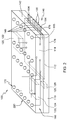
- FIG. 3 shows a side, top up perspective view of embodiments of PIC fan-out package with a heat spreader and a PCB, according to embodiments of the disclosure.
- FIG. 3 also shows an optical connector.
- FIG. 4 shows an enlarged side view of a lateral side of a PIC fan-out package with optical fibers in place, according to embodiments of the disclosure.
- FIG. 5 shows a side, top up perspective view of embodiments of a PIC fan-out package, according to another embodiment of the disclosure, but without a PCB attached thereto.
- FIG. 6 shows a side, bottom up perspective view of embodiments of PIC fan-out package, according to another embodiment of the disclosure, but without a printed circuit board attached thereto.
- FIG. 7 shows a side, cross-sectional view of embodiments of PIC fan-out package, according to another embodiment of the disclosure.
- FIGS. 8, 9A, 9B and 10-14 show steps of a method of making a PIC fan-out package according to one embodiment of the disclosure.
- FIGS. 15-22 show steps of a method of making a PIC fan-out package according to another embodiment of the disclosure.
- Embodiments of the disclosure provide a photonic integrated circuit (PIC) fan-out package and related methods of forming the same.
- the PIC fan-out package includes a PIC die and an ancillary device(s) in an overmold body.
- a plurality of optical fiber stubs are operatively coupled to electro-optical circuitry including an optical waveguide system (including a waveguide for each fiber) in the PIC die.
- an edge fiber coupling interface is provided in a lateral side of the overmold body for coupling the plurality of optical fiber stubs to external optical fibers with a connector.
- a redistribution layer (RDL) interposer is adjacent the overmold body and electrically connects to the PIC die and the ancillary device(s).
- a ball grid array (BGA) electrically couples to the PIC die and the ancillary device by the RDL interposer.
- the BGA is configured to electrically couple the PIC die and the ancillary device(s) to a printed circuit board (PCB).
- PCB printed circuit board
- the PIC fan-out package provides a simpler side coupling structure for external fiber optic links, and solder reflowable interconnects for electrical interconnection for PCB attachment. Since the optical fiber stub attachment is done at the reconstituted wafer level with known good dies (KGD), the fiber alignment can be a high throughput process compared to conventional PIC die packaging processes.
- Ancillary devices can include, for example, a trans-impedance amplifier (TIA), a driver and/or a passive device (e.g., resistors, capacitors, etc.).
- the ancillary device(s) are integrated in the package to provide higher packaging integration density.
- the back side of the PIC die and ancillary devices may be exposed in the overmold body so a heat spreader can be attached for thermal management.
- the BGA enables a solder reflowable optical module with exposed fiber ends after reflow to the PCB.
- External optical fibers can be coupled to the package using passive or active alignment (e.g., mechanical positioning and alignment versus use of optical and/or electrical feedback to determine optimal alignment) referencing to protruding optical fiber stubs, or can be coupled to a polished side of the PIC die.
- the PIC fan-out package may be applied across a variety of applications such as but not limited to short reach, low cost, high speed optical link applications (e.g., automotive, artificial intelligence (AI), cameras, harsh environments, military, augmented reality/virtual reality (AR/VR), etc.).
- AI artificial intelligence
- AR/VR augmented reality/virtual reality
- FIG. 1 shows a side, top up perspective view of embodiments of a PIC fan-out package 100 without a PCB attached thereto;
- FIG. 2 shows a side, bottom up perspective view of embodiments of PIC fan-out package 100 without a PCB; and
- FIG. 3 shows a side, top up perspective view of embodiments of PIC fan-out package 100 with a heat spreader 102 , a PCB 104 and an optical connector 106 .
- PIC package 100 may include an overmold body 110 , and a PIC die 112 in overmold body 110 .
- PIC die 112 may include any now known or later developed semiconductor photonic integrated circuit. As understood in the art, PIC die 112 , also known as integrated optical circuits, can be any device that includes electro-optical circuitry 114 that integrates multiple photonic functions for optical information signals received thereby via, e.g., optical fibers. Such functions oftentimes includes converting the optical information signals to electrical signals or vice versa.
- Electro-optical circuitry 114 may include an optical waveguide system 115 (e.g., grating coupler or I/O waveguide), but may also include, depending on application, other components such as but not limited to: a Bragg reflector, an arrayed waveguide grating or other wave guide, transistor based electronics including detectors and modulators, amplifiers, and/or an externally modulated laser diode with an electro-absorption modulator. It is understood that optical waveguide system 115 may include structures to guide light/signals from each optical fiber coupled thereto, individually.
- optical waveguide system 115 may include structures to guide light/signals from each optical fiber coupled thereto, individually.
- Overmold body 110 may include any now known or later developed material capable of encapsulating electronic devices such as but not limited to thermoset polymers that come in, for example, epoxy molded compounds resins, or silicone-based materials.
- PIC package 100 may also include an ancillary device 120 in overmold body 110 .
- Ancillary device(s) 120 may include any one or more devices providing complementary functions to PIC die 112 . Any number of ancillary device(s) 120 may be provided.
- Ancillary device(s) 120 may include but are not limited to: a trans-impedance amplifier (TIA) 122 , a driver 124 and a passive device 126 (e.g., a resistor, capacitor or other passive element).
- TIA trans-impedance amplifier
- PIC package 100 also includes plurality of optical fiber stubs 130 operatively coupled to optical waveguide system 115 ( FIG. 1 , in phantom).
- Optical fiber stubs 130 can be coupled to optical waveguide system 115 via a plurality of V-groove receptacles 132 (buried in overmold 110 , shown in phantom).
- V-groove receptacles 132 act to position optical fiber stubs 130 relative to, for example, optical waveguide system 115 of electro-optical circuitry 114 ( FIGS. 1-3 ).
- Optical fiber stubs 130 may include any now known or later developed single mode or multi-mode glass fiber.
- Optical fiber stubs 130 are referred to as ‘stubs’ because of their relatively short length.
- Optical fiber stubs 130 may be, for example, 1200-1300 micrometers ( ⁇ m) in length, with approximately 100-200 ⁇ m protruding from a lateral side 142 of PIC die 112 .
- each optical fiber stub 130 may have, for example, a 9 ⁇ m core and a 125 ⁇ m outer diameter glass cladding. It is noted that these dimensions are typical dimensions of optical fiber stubs 130 assuming a PIC die 112 with 1 mm long V-groove receptacles 132 .
- Fiber optic stubs 130 may vary depending on, for example, the die size, V-groove receptacle 132 length, the fiber stub length and/or stub protruding length.
- Optical fiber stubs 130 with 80 micrometer ( ⁇ m) diameter and with a 4 ⁇ m core are also possible.
- Multimode fibers 125 ⁇ m fiber with 62.5 ⁇ m core
- Optical fiber stubs 130 may be held in V-groove receptacle 132 by an adhesive 136 , discussed in greater detail herein.
- Fiber optic stubs 130 extend from a lateral side of PIC die 112 towards a lateral side of overmold body 110 .
- PIC package 100 includes an edge fiber coupling interface 140 in lateral side 142 of overmold body 110 for coupling plurality of optical fiber stubs 130 to external optical fibers 150 using a connector.
- “Lateral side” indicates a side of the square shaped overmold body (or PIC die) that is not vertically facing, i.e., up or down, in an operative state.
- edge fiber coupling interface 140 includes each of optical fiber stubs 130 extending from the lateral side of PIC die 112 and protruding from lateral side 142 of overmold body 110 .
- optical fiber stubs 130 have a protrusion 146 extending externally of lateral side 142 , e.g., 100-200 ⁇ m. While four ( 4 ) protrusions 146 are shown in FIGS. 1-3 , any number can be used.
- Each optical fiber stub 130 via protrusions 146 , are configured to optically couple to external optical fibers 150 ( FIG. 3 ) using, for example, optical connector 106 in the form of an external optical connector 108 ( FIG. 3 ).
- External optical connector 106 may include any now known or later developed optical fiber connection mechanism such as but limited to a precision aligned pluggable socket terminating in additional fibers or pigtails.
- edge fiber coupling interface 140 may further include an alignment member 154 for aligning external optical connector 106 with protrusions 146 of plurality of optical fiber stubs 130 protruding from lateral side 142 of overmold body 110 .
- Alignment member 154 may include, for example, one or more protruding pins that are complementary to matching receptacles (not shown) in external optical connector. Two pins are shown, but any number may be provided.
- Alignment member 154 may be made of any rigid material such as metal or hard plastic. Any other structure necessary to hold external optical connector 106 to overmold body 110 may be employed such as but not limited to snap fasteners, threaded fasteners, etc.
- edge fiber coupling interface 140 may include optical fiber stubs 130 ( FIG. 4 ) being flush 148 to lateral side 142 of overmold body 110 for optical coupling to external optical fibers 150 using external optical fiber shunts 152 .
- lateral side 142 of overmold body 110 is polished so that optical fiber ends are flush with lateral side of overmold body 110 of PIC package 100 .
- An optical connector 106 with optical fiber shunts 152 e.g., an array of optical fibers in a glass v-groove assembly
- FIG. 5 also shows an optional embodiment in which a laser die 156 is within or part of PIC die 112 . In this fashion, PIC die 112 is not reliant on an external light source, as is typically the case.
- PIC package 100 also may include a redistribution wiring layer (RDL) interposer 160 adjacent overmold body 110 and electrically connected to PIC die 112 and ancillary device(s) 120 .
- RDL interposer 160 may include any now known or later developed interconnect structure such as but not limited to wiring and vias within respective dielectric layers.
- Dielectric layers may include but are not limited to: polyimide (PI), polybenzaoxazole (PBO), benzocyclobutene (BCB), and epoxy based materials.
- Wiring and vias may include any now known or later developed materials such as copper or aluminum within a refractory metal liner.
- ancillary device(s) 120 and PIC die 112 may have coplanar surfaces at a location where each meet RDL interposer 160 . That is, ancillary device(s) 120 and PIC die 112 have the same connection plane with RDL interposer 160 .
- PIC package 100 may also include a ball grid array (BGA) 170 electrically coupled to the PIC die 112 and ancillary device(s) 120 by RDL interposer 160 .
- BGA 170 is configured to electrically couple PIC die 112 and ancillary device(s) 120 to a printed circuit board (PCB) 172 .
- BGA 170 may include any now known or later ball grid array, e.g., of tin solder bumps arrayed to electrically couple connectors of RDL interposer 160 to PCB 172 in a conventional fashion.
- RDL interposer 160 may interconnect PIC die 112 and/or ancillary device(s) 120 to one another or to BGA 170 in any desired manner.
- a surface 176 of PIC die 112 is exposed in an upper surface 178 of overmold body 110 .
- heat spreader 102 may be thermally coupled to PIC die 112 .
- a surface 180 of one or more of ancillary device(s) 120 may also be exposed in upper surface 178 of overmold body 110 .
- heat spreader 102 may be thermally coupled to at least one of ancillary device(s) 120 , e.g., trans-impedance amplifier (TIA) 122 , driver 124 and passive device(s) 126 .
- TIA trans-impedance amplifier
- Heat spreader 102 may take any now known or later developed form of heat dissipating device, e.g., nickel plated copper lid, a finned aluminum plate, a liquid or air cooled member, thermo-electric cooling (TEC) system, etc. Heat spreader 102 may be adhered to upper surface 178 of overmold body 110 and/or upper surface(s) 176 , 180 of PIC die 112 and ancillary device(s) 120 , respectively, using any now known or later developed thermal interface material.
- TEC thermo-electric cooling
- FIG. 6 shows a side, bottom up perspective view of embodiments of PIC package 100 without PCB 172 ( FIG. 3 ), including other optional embodiments.
- TIA 122 may be flip-chip coupled to PIC die 112 . That is, TIA 122 may be directly coupled to a vertically facing (bottom) surface 188 of PIC die 112 , e.g., via a controlled collapse chip connects (C 4 ) 190 .
- FIG. 7 shows a cross-sectional side view of PIC package 100 according to another optional embodiment that includes another device 192 mounted to an exterior surface 194 of overmold body 110 .
- Device 192 may include any now known or later developed device that may be desired to operatively couple to PIC die 112 and/or ancillary device(s) 120 such as but not limited to: another IC, passive devices, etc.
- PIC package 100 can be made in a number of ways.
- FIGS. 8, 9A, 9B and 10-14 show one embodiment of a method of making PIC package 100 in which circuitry, e.g., of PIC die 112 is facing up during manufacture
- FIGS. 15-22 show another embodiment of a method of making PIC package 100 in which circuitry is facing down during manufacture. Each method creates PIC package 100 , as described herein.
- each PIC die 112 and ancillary device(s) 120 are mounted to a carrier 200 .
- Each PIC die 112 and ancillary device(s) 120 are known good devices (KGDs), i.e., compared to inoperative devices.
- KGDs known good devices
- Each PIC die 112 and each ancillary device 120 have electrical connection points 202 on an opposing, vertically facing side thereof from carrier 200 , i.e., circuitry for each is facing upwardly or oppositely of carrier 200 .
- each PIC die 112 includes a plurality of V-groove fiber optic receptacles 132 (see FIG.
- PIC die 112 and ancillary device(s) 120 may be mounted to carrier 200 using any now known or later developed material, e.g., an adhesive.
- Carrier 200 may include any now known or later developed wafer handling material, e.g., glass or silicon.
- FIG. 9A shows a side view of and FIG. 9B shows an enlarged end view of individually mounting an optical fiber stub 130 into each of the desired (e.g., least two) of V-groove receptacles 132 , each optical fiber stub 130 protruding from lateral side 142 of respective PIC die 112 .
- V-groove receptacles 132 act to position optical fiber stubs 130 relative to, for example, a waveguide (not shown) in PIC die circuitry 114 ( FIG. 1 ).
- optical fiber stubs 130 may include any now known or later developed single mode or multi-mode glass fiber.
- optical fiber stubs 130 are referred to as ‘stubs’ because of their relatively short length.
- Optical fiber stubs 130 may include any of the previously described fibers, for example, those that are 1200-1300 ⁇ m in length, and may protrude, for example, 100-200 ⁇ m from lateral side 142 .
- This step may include any now known or later developed pick and place process known in the art.
- each optical fiber stub 130 may picked and placed into a respective V-groove receptacle 132 , followed by applying adhesive 136 ( FIG. 9B ) to each optical fiber stub 130 , and curing the adhesive, e.g., using light and/or heat.
- adhesive 136 FIG. 9B
- optical fiber stubs 130 may be held in V-groove receptacle 132 by adhesive 136 , which may include, for example, a light or thermal curable adhesive.
- adhesive 136 may include, for example, a light or thermal curable adhesive.
- the method may also include mounting alignment member 154 ( FIGS. 3, 4 and 9B ), e.g., metal pins, in at least one of plurality of V-groove receptacles 132 and adhering them in place.
- FIG. 10 shows overmolding of plurality of sets of PIC die 112 and ancillary device(s) 120 on carrier 200 , creating overmold body 110 .
- overmold body 110 may include any now known or later developed material capable of encapsulating electronic devices such as but not limited to thermoset polymers that come in, for example, epoxy molded compounds resins, or silicone-based materials.
- FIG. 11 shows forming RDL interposer 160 for each of the plurality of sets.
- Each RDL interposer 160 electrically connects to at least one of the PIC die 112 and ancillary device(s) 120 .
- RDL interposer 160 may be formed using any now known or later developed semiconductor wiring/via formation techniques such as damascene or dual damascene techniques.
- FIG. 12 shows removing carrier 200 , creating a set of connected modules 210 , each module 210 including a selected PIC die 112 and a selected ancillary device(s) 120 , i.e., to form a desired PIC package 100 .
- FIG. 12 shows a dicing frame 212 supporting set of connected modules 210 .
- FIG. 13 shows dicing a selected module 220 from the set of modules shown in FIG. 12 .
- the dicing may include using any now known or later developed dicing technique, e.g., lasers, to separate the modules.
- FIG. 13 also shows forming an edge fiber coupling interface 140 according to the embodiment in which optical fiber stubs 130 are flush with lateral side 142 of overmold body 110 of selected module 220 , as in FIG. 5 .
- This step may include performing a planarization of lateral side 142 (after rough cut from dicing) to planarize (and make flush) and polish the ends of each optical fiber stub 130 on lateral side 142 of overmold body 110 of selected module 220 .
- FIG. 1 shows dicing a selected module 220 from the set of modules shown in FIG. 12 .
- the dicing may include using any now known or later developed dicing technique, e.g., lasers, to separate the modules.
- FIG. 13 also shows forming an
- each alignment member 154 protrudes from lateral side 142 of overmold body 110 .
- This step may include planarizing lateral end 142 of overmold body 110 (after rough cut from dicing) to planarize each optical fiber stub 130 on lateral side 142 of overmold body 110 of selected module 220 , and etching overmold body 110 to expose the portion of each optical fiber stub 130 on the lateral side of the overmold body of the selected module.
- Etching generally refers to the removal of material from a substrate (or structures formed on the substrate), and is often performed with a mask in place so that material may selectively be removed from certain areas of the substrate, while leaving the material unaffected, in other areas of the substrate.
- etching There are generally two categories of etching, (i) wet etch and (ii) dry etch.
- Wet etch is performed with a solvent (such as an acid) which may be chosen for its ability to selectively dissolve a given material (such as oxide), while, leaving another material (such as polysilicon) relatively intact. This ability to selectively etch given materials is fundamental to many semiconductor fabrication processes.
- a wet etch will generally etch a homogeneous material (e.g., oxide) isotropically, but a wet etch may also etch single-crystal materials (e.g. silicon wafers) anisotropically.
- Dry etch may be performed using a plasma.
- Plasma systems can operate in several modes by adjusting the parameters of the plasma. Ordinary plasma etching produces energetic free radicals, neutrally charged, that react at the surface of the module. Since neutral particles attack the side of the module from all angles, this process is isotropic. Ion milling, or sputter etching, bombards the wafer with energetic ions of noble gases which approach the wafer approximately from one direction, and therefore this process is highly anisotropic.
- Reactive-ion etching RIE operates under conditions intermediate between sputter and plasma etching and may be used to produce deep, narrow features, such as STI trenches. Here, a RIE may be carried out.
- the drawing shows a final step of forming BGA 170 on RDL interposer 160 of selected module 220 .
- BGA 170 is electrically connected to PIC die 112 and ancillary device(s) 120 by RDL interposer 160 .
- BGA 170 is configured to electrically couple PIC die 112 and ancillary device(s) 120 to PCB, as shown in FIG. 3 .
- FIGS. 15-22 another embodiment of a method of making PIC package 100 is shown.
- optical fiber stubs 130 are connected to PIC die 112 prior to packaging with ancillary device(s) 120 .
- circuitry of PIC die 112 and ancillary device(s) 120 can be facing downwardly during manufacture.
- each PIC die 112 and each ancillary device 120 have electrical connection points 202 (in a circuit plane 203 , FIGS. 17 and 20 ) against a carrier 250 ( FIG. 17 ), i.e., circuitry for each is facing carrier 250 .
- FIG. 15 shows mounting PIC dies 112 to a first carrier 240
- each PIC die 112 includes a plurality of V-groove receptacles 132 on an opposing vertically facing side 242 of respective PIC die 112 from first carrier 240 .
- First carrier 240 may include any now known or later developed wafer handling material, e.g., glass or silicon.
- Each PIC die 112 employed represents a known good die (KGD), i.e., compared to discarded, inoperative dies.
- PIC dies 112 may be mounted using any now known or later developed process, e.g., adhesive.
- Each V-groove receptacle 132 is configured to receive and operatively couple optical fiber stub 130 ( FIG.
- FIG. 16 shows individually mounting optical fiber stubs 130 into each of the at least two of plurality of V-groove receptacles 132 ( FIG. 4 ).
- This step may include any now known or later developed pick and place process known in the art.
- each optical fiber stub 130 may be picked and placed into a respective V-groove receptacle 132 ( FIG. 4 ), followed by applying adhesive 136 ( FIG. 4 ) to each optical fiber stub 130 , and curing the adhesive, e.g., using light or heat.
- the method may also including mounting alignment member 154 ( FIGS.
- a circuit plane 203 may be added at this stage to provide electrical connection points 202 ( FIG. 17 ).
- FIG. 17 shows PIC dies 112 after separating each PIC die 112 from first carrier 240 ( FIG. 16 ), e.g., using dicing or adhesive removal techniques and with circuit plane 203 , and mounting a plurality of sets of a selected PIC die 112 (e.g., known good die) and an ancillary device(s) 120 to a second carrier 250 .
- Second carrier 250 may include any now known or later developed wafer handling material, e.g., glass or silicon.
- Second carrier 250 may include any material listed herein for first carrier 240 .
- FIG. 18 shows overmolding of plurality of sets, i.e., of PIC die 112 and ancillary device(s) 120 , on second carrier 250 , creating overmold body 110 .
- overmold body 110 may include any now known or later developed material capable of encapsulating electronic devices such as but not limited to thermoset polymers that come in, for example, epoxy molded compounds resins, or silicone-based materials.
- FIG. 19 shows removing second carrier 250 , creating a set of connected modules 252 .
- Second carrier 250 may be removed in any known fashion.
- Each module 252 includes a selected PIC die 112 and a respective ancillary device(s) 120 , i.e., to form a desired PIC package 100 .
- FIG. 20 shows, after flipping overmold body 110 , forming RDL interposer 160 for each connected module 252 .
- Each RDL interposer 160 electrically connects to the selected PIC die 112 and the respective ancillary device(s) 120 of a respective connected module 252 .
- Each RDL interposer 160 electrically connects to at least one of PIC die 112 and ancillary device(s) 120 .
- RDL interposer 160 may be formed using any now known or later developed semiconductor wiring/via formation techniques such as photolithographic via formation or laser via ablation and plating.
- FIG. 20 also shows a dicing frame 254 supporting set of connected modules 252 .
- FIG. 21 shows dicing to create a selected module 260 from the set of connected modules 252 shown in FIG. 20 .
- the dicing may include using any now known or later developed dicing technique, e.g., saw dicing, lasers, to separate the modules.
- FIG. 21 shows forming an edge fiber coupling interface 140 according to the embodiment in which optical fiber stubs 130 are flush on lateral side 142 of overmold body 110 of selected module 220 , as in FIG. 5 . This step may include planarizing lateral side 142 (after dicing).
- FIG. 21 shows dicing to create a selected module 260 from the set of connected modules 252 shown in FIG. 20 .
- the dicing may include using any now known or later developed dicing technique, e.g., saw dicing, lasers, to separate the modules.
- FIG. 21 shows forming an edge fiber coupling interface 140 according to the embodiment in which optical fiber stubs 130 are flush on lateral side 142 of overmold
- each alignment member 154 protrudes from lateral side 142 of overmold body 110 .
- This step may include planarizing lateral end 142 of overmold body 110 (after rough cut from dicing) to planarize each optical fiber stub 130 on lateral side 142 of overmold body 110 of selected module 220 , and etching overmold body 110 to expose the portion of each optical fiber stub 130 on the lateral side of the overmold body of the selected module.
- Each alignment member 154 FIG. 3 ) may also be exposed at this time.
- FIG. 22 shows a final step of forming BGA 170 on RDL interposer 160 of selected module 260 .
- BGA 170 is electrically connected to PIC die 112 and ancillary device(s) 120 by RDL interposer 160 .
- BGA 170 is configured to electrically couple PIC die 112 and ancillary device(s) 120 to PCB, as shown, for example, in FIG. 3 .
- PIC package 100 as described herein may also include additional features such as flip chip die attachment of ancillary device(s) 120 to PIC die 112 ( FIG. 7 ) for reducing die to die interconnect length (pre/post BGA formation). Further, as described relative to FIG. 5 , PIC die 112 may also include a laser die 156 is within or part of PIC die 112 . In this fashion, PIC die 112 is not reliant on an external light source, as is typically the case.
- Other enhancements of PIC package i.e., as a wafer level fan out package, may include but are not limited to: thru-mold vias, integrated passives (ancillary device(s) 126 ( FIG. 1 )), package on package stacking ( FIG. 7 ), electro-magnetic interference (EMI) shielding structures, thermal enhancements (e.g., heat spreader 102 ).
- EMI electro-magnetic interference
- PIC fan-out package 100 provides a simpler side coupling structure for external fiber optic links 150 , and solder reflowable interconnects for electrical interconnection for PCB (e.g., PCB 172 FIG. 7 ) attach via BGA 170 .
- Ancillary devices 120 can include, for example, a trans-impedance amplifier (TIA), driver and/or a passive device (e.g., resistors, capacitors, etc.).
- Ancillary device(s) 120 are integrated in the package to provide higher packaging integration density.
- a back vertically facing side of PIC die 112 and ancillary device(s) 120 may be exposed in overmold body 110 (e.g., surface 178 of overmold body 110 in FIG.
- BGA 170 creates a solder reflowable optical package with external fiber 150 attach after reflow.
- External optical fibers 150 can be coupled to the package using passive or active alignment referencing to protruding 146 optical fiber stubs 130 , or can be coupled to a polished side 148 ( FIG. 5 ) of PIC die 112 .
- PIC package 100 may be applied across a variety of applications such as but not limited to short reach, low cost, high speed optical link applications (e.g., automotive, artificial intelligence (AI), cameras, harsh environments, military, augmented or virtual reality (AR/VR), etc.).
- AI artificial intelligence
- AR/VR augmented or virtual reality
- Approximating language may be applied to modify any quantitative representation that could permissibly vary without resulting in a change in the basic function to which it is related. Accordingly, a value modified by a term or terms, such as “about”, “approximately” and “substantially”, are not to be limited to the precise value specified. In at least some instances, the approximating language may correspond to the precision of an instrument for measuring the value.
- range limitations may be combined and/or interchanged, such ranges are identified and include all the sub-ranges contained therein unless context or language indicates otherwise. “Approximately” as applied to a particular value of a range applies to both values, and unless otherwise dependent on the precision of the instrument measuring the value, may indicate +/ ⁇ 10% of the stated value(s).
Landscapes
- Physics & Mathematics (AREA)
- General Physics & Mathematics (AREA)
- Optics & Photonics (AREA)
- Optical Couplings Of Light Guides (AREA)
Abstract
Description
Claims (20)
Priority Applications (2)
| Application Number | Priority Date | Filing Date | Title |
|---|---|---|---|
| US15/920,537 US10598860B2 (en) | 2018-03-14 | 2018-03-14 | Photonic die fan out package with edge fiber coupling interface and related methods |
| TW108104653A TWI710081B (en) | 2018-03-14 | 2019-02-12 | Photonic die fan out package with edge fiber coupling interface and related methods |
Applications Claiming Priority (1)
| Application Number | Priority Date | Filing Date | Title |
|---|---|---|---|
| US15/920,537 US10598860B2 (en) | 2018-03-14 | 2018-03-14 | Photonic die fan out package with edge fiber coupling interface and related methods |
Publications (2)
| Publication Number | Publication Date |
|---|---|
| US20190285804A1 US20190285804A1 (en) | 2019-09-19 |
| US10598860B2 true US10598860B2 (en) | 2020-03-24 |
Family
ID=67905427
Family Applications (1)
| Application Number | Title | Priority Date | Filing Date |
|---|---|---|---|
| US15/920,537 Active US10598860B2 (en) | 2018-03-14 | 2018-03-14 | Photonic die fan out package with edge fiber coupling interface and related methods |
Country Status (2)
| Country | Link |
|---|---|
| US (1) | US10598860B2 (en) |
| TW (1) | TWI710081B (en) |
Cited By (7)
| Publication number | Priority date | Publication date | Assignee | Title |
|---|---|---|---|---|
| US10754113B1 (en) * | 2019-08-16 | 2020-08-25 | Eagle Technology, Llc | Opto-electronic device including active circuit component on circuit attachment area of optical fiber and related methods |
| US20210288035A1 (en) * | 2020-03-12 | 2021-09-16 | Intel Corporation | Active bridge enabled co-packaged photonic transceiver |
| US20220100692A1 (en) * | 2020-09-25 | 2022-03-31 | Intel Corporation | Electrical and optical interfaces at different heights along an edge of a package to increase bandwidth along the edge |
| US11650381B1 (en) | 2022-02-12 | 2023-05-16 | Globalfoundries U.S. Inc. | PIC die and package with cover for multiple level and multiple depth connections of fibers to on-chip optical components |
| US12130470B2 (en) | 2021-10-25 | 2024-10-29 | Globalfoundries U.S. Inc. | PIC die and package with multiple level and multiple depth connections of fibers to on-chip optical components |
| US12326592B2 (en) | 2022-12-07 | 2025-06-10 | International Business Machines Corporation | Heterogeneous package structures with photonic devices |
| US12332490B2 (en) * | 2021-09-24 | 2025-06-17 | Hirose Electric Co., Ltd. | Media adaptor for multimode waveguide interconnects |
Families Citing this family (39)
| Publication number | Priority date | Publication date | Assignee | Title |
|---|---|---|---|---|
| US10749603B2 (en) * | 2016-07-14 | 2020-08-18 | Ayar Labs, Inc. | Laser module for optical data communication system within silicon interposer |
| US10866373B2 (en) * | 2018-06-27 | 2020-12-15 | Taiwan Semiconductor Manufacturing Company, Ltd. | Optical transceiver and manufacturing method thereof |
| WO2020024284A1 (en) * | 2018-08-03 | 2020-02-06 | Lumentum Operations Llc | Laser welding for planar lightwave circuit–fiber packaging |
| US11493713B1 (en) * | 2018-09-19 | 2022-11-08 | Psiquantum, Corp. | Photonic quantum computer assembly having dies with specific contact configuration and matched CTE |
| US10790269B2 (en) * | 2019-01-29 | 2020-09-29 | Taiwan Semiconductor Manufacturing Company, Ltd. | Semiconductor devices and semiconductor structures |
| US11443998B2 (en) * | 2019-06-05 | 2022-09-13 | Te Connectivity Solutions Gmbh | Electronic assembly including optical modules |
| US11500153B2 (en) * | 2019-10-15 | 2022-11-15 | Ayar Labs, Inc. | Multi-chip packaging of silicon photonics |
| US11635566B2 (en) | 2019-11-27 | 2023-04-25 | Taiwan Semiconductor Manufacturing Co., Ltd. | Package and method of forming same |
| DE102020115377B4 (en) | 2019-11-27 | 2026-01-15 | Taiwan Semiconductor Manufacturing Co., Ltd. | PACKAGE AND METHOD FOR ITS MANUFACTURING |
| TWI884215B (en) * | 2020-02-13 | 2025-05-21 | 美商爾雅實驗室公司 | Chip-last wafer-level fan-out with optical fiber alignment structure |
| KR20220148836A (en) * | 2020-02-14 | 2022-11-07 | 아야 랩스 인코포레이티드 | Remote memory architecture enabled by monolithic in-package optical I/O |
| US11567285B2 (en) | 2020-04-30 | 2023-01-31 | Corning Research & Development Corporation | High-density FAUs and optical interconnection devices including optimized arrays and related methods |
| US11694939B2 (en) * | 2020-05-22 | 2023-07-04 | Taiwan Semiconductor Manufacturing Company, Ltd. | Semiconductor package, integrated optical communication system |
| TW202217377A (en) * | 2020-07-06 | 2022-05-01 | 新加坡商光子智能私人有限公司 | Integrated circuit interposer, system, apparatus, method of fabricating integrated circuit interposer, and method and system for transmitting information from nodes to destination interposer |
| CN114077016B (en) | 2020-08-11 | 2023-09-01 | 美国莫列斯有限公司 | Package structure with photonic integrated circuit |
| TWI802812B (en) * | 2020-08-11 | 2023-05-21 | 美商莫仕有限公司 | Package structure having photonic integrated circuit |
| JP7520983B2 (en) * | 2020-08-28 | 2024-07-23 | 京セラ株式会社 | Optical Circuit Board |
| US12061371B2 (en) * | 2020-12-22 | 2024-08-13 | Intel Corporation | Patch on interposer architecture for low cost optical co-packaging |
| US20220291462A1 (en) * | 2021-03-11 | 2022-09-15 | Intel Corporation | Method to couple light using integrated heat spreader |
| US12235498B2 (en) * | 2021-04-05 | 2025-02-25 | Electronics And Telecommunications Research Institute | Manufacturing method and application of optical interconnection module |
| US11709327B2 (en) | 2021-04-26 | 2023-07-25 | Advanced Micro Devices, Inc. | Fanout module integrating a photonic integrated circuit |
| KR20240000525A (en) | 2021-04-26 | 2024-01-02 | 어드밴스드 마이크로 디바이시즈, 인코포레이티드 | Fan-out module incorporating photonic integrated circuit |
| EP4083676A1 (en) | 2021-04-30 | 2022-11-02 | Sentea | Improved photonic packaging |
| US11555972B2 (en) | 2021-06-09 | 2023-01-17 | Cisco Technology, Inc. | Connecting optical connector with co-packaged optical device |
| US11762155B2 (en) * | 2021-08-25 | 2023-09-19 | Cisco Technology, Inc. | Photonics packaging platform |
| US12306480B2 (en) | 2021-09-09 | 2025-05-20 | Intel Corporation | Glass interposer optical resonator device and method |
| US12353070B2 (en) * | 2021-09-09 | 2025-07-08 | Intel Corporation | Glass interposer optical switching device and method |
| US20230077877A1 (en) * | 2021-09-10 | 2023-03-16 | Advanced Semiconductor Engineering, Inc. | Photonic package and method of manufacturing the same |
| US20230090863A1 (en) * | 2021-09-22 | 2023-03-23 | Intel Corporation | Optical waveguide edge coupling within a substrate |
| US12345932B2 (en) * | 2021-09-23 | 2025-07-01 | Intel Corporation | Die last and waveguide last architecture for silicon photonic packaging |
| US12422635B2 (en) * | 2022-05-27 | 2025-09-23 | Taiwan Semiconductor Manufacturing Co., Ltd. | Thermo-electric cooler for dissipating heat of optical engine |
| WO2024059724A1 (en) * | 2022-09-14 | 2024-03-21 | Senko Advanced Components, Inc. | Configurable optical connector module |
| US12487417B2 (en) * | 2022-10-04 | 2025-12-02 | Applied Materials, Inc. | Photonic glass layer substrate with embedded optical structures for communicating with an electro optical integrated circuit |
| CN115542458B (en) * | 2022-11-30 | 2023-02-07 | 中国电子科技集团公司信息科学研究院 | Heterogeneous integrated photoelectric micro-system and manufacturing method thereof |
| US12353031B1 (en) * | 2023-01-20 | 2025-07-08 | Cisco Technology, Inc. | Facet coupling fanout device |
| US12461304B2 (en) | 2023-02-07 | 2025-11-04 | Cisco Technology, Inc. | Optical packaging features for mechanical stability and optical fiber coupling |
| US20250180839A1 (en) * | 2023-12-01 | 2025-06-05 | Shenzhen 8k Link Optoelectronics Technology Co., Ltd. | Mult-chip package design module of glass v-groove design without conventional wire bonding |
| US20250244528A1 (en) * | 2024-01-31 | 2025-07-31 | Applied Materials, Inc. | Photonic integrated circuits to glass substrate bonding |
| KR102803765B1 (en) * | 2024-11-29 | 2025-05-08 | 주식회사 에이디에스테크 | Device for aligning receptacle for removable fiber arrays for photonics integrated circuits in cpo modules and method for aligning receptacle using thereof |
Citations (35)
| Publication number | Priority date | Publication date | Assignee | Title |
|---|---|---|---|---|
| US5879173A (en) * | 1995-01-13 | 1999-03-09 | Methode Electronics, Inc. | Removable transceiver module and receptacle |
| US5960141A (en) * | 1997-10-17 | 1999-09-28 | Fujitsu Limited | Optical transmission terminal device |
| US6267606B1 (en) * | 1995-01-13 | 2001-07-31 | Stratos Lightwave, Inc. | Removable transceiver module and receptacle |
| US6309566B1 (en) * | 1999-02-22 | 2001-10-30 | Siemens Aktiengesellschaft | Method and mold for producing an electrooptical module, and electrooptical module |
| US20020028045A1 (en) * | 1998-10-09 | 2002-03-07 | Tetsuzo Yoshimura | Optical coupling structures and the fabrication processes |
| US20020039464A1 (en) * | 1998-10-09 | 2002-04-04 | Tetsuzo Yoshimura | Optical reflective structures and method for making |
| US6422766B1 (en) * | 1998-05-27 | 2002-07-23 | Siemens Aktiengesellschaft Ag | Housing configuration for a laser module |
| US20020097962A1 (en) * | 1998-10-09 | 2002-07-25 | Tetsuzo Yoshimura | Single and multilayer waveguides and fabrication process |
| US20020104959A1 (en) * | 2000-12-13 | 2002-08-08 | Barry Arsenault | Packaging system for two-dimensional optoelectronic arrays |
| US6456766B1 (en) * | 2000-02-01 | 2002-09-24 | Cornell Research Foundation Inc. | Optoelectronic packaging |
| US20030026168A1 (en) * | 2001-07-16 | 2003-02-06 | Input/Output, Inc. | Apparatus and method for seismic data acquisition |
| US20030171022A1 (en) * | 2002-03-05 | 2003-09-11 | Jds Uniphase Corporation | Optical transceiver latch |
| US20050111781A1 (en) * | 2003-11-20 | 2005-05-26 | Kanti Jain | Photonic-electronic circuit boards |
| US20060013542A1 (en) * | 2002-03-08 | 2006-01-19 | Infineon Technologies Ag | Optoelectronic module and plug arrangement |
| US7015454B2 (en) * | 1998-10-22 | 2006-03-21 | Wavefront Research, Inc. | Relaxed tolerance optical interconnect system capable of providing an array of sub-images |
| US7050678B1 (en) * | 1998-08-28 | 2006-05-23 | Fujikura Ltd. | Optical module, optical element attachment method, and receptacle-fitted optical module |
| US20060140630A1 (en) * | 2004-12-23 | 2006-06-29 | Ch Capital, Inc. Aka Ch Capital, Llc | Communication systems incorporating control meshes |
| US7446298B1 (en) * | 1998-10-22 | 2008-11-04 | Wavefront Research, Inc. | Relaxed tolerance optical interconnect systems |
| US20090003761A1 (en) * | 2004-09-29 | 2009-01-01 | Yasunobu Matsuoka | Optoelectronic Integrated Circuit Device and Communications Equipment Using Same |
| US7939791B1 (en) * | 1998-10-22 | 2011-05-10 | Wavefront Research, Inc. | Optical data pipe |
| US20120001166A1 (en) * | 2010-06-30 | 2012-01-05 | International Business Machines Corporation | Parellel optical transceiver module |
| US20130114924A1 (en) | 2010-04-29 | 2013-05-09 | Agency For Science, Technology And Research | Optical Arrangement and a Method of Forming the Same |
| US20140203175A1 (en) * | 2011-12-30 | 2014-07-24 | Mauro J. Kobrinsky | Optical i/o system using planar light-wave integrated circuit |
| US20140254968A1 (en) | 2011-09-30 | 2014-09-11 | Nsk Ltd. | Grease composition for rolling bearing and rolling bearing |
| US20140270784A1 (en) * | 2013-03-14 | 2014-09-18 | Oracle International Corporation | Stackable photonic interconnect module |
| US20150037044A1 (en) * | 2013-08-02 | 2015-02-05 | Luxtera, Inc. | Method and system for an optical coupler for silicon photonics devices |
| US20150219850A1 (en) | 2014-02-05 | 2015-08-06 | Aurrion, Inc. | Shielding regions for photonic integrated circuits |
| US20160274318A1 (en) * | 2012-03-05 | 2016-09-22 | Nanoprecision Products, Inc. | Optical bench subassembly having integrated photonic device |
| WO2016153484A1 (en) | 2015-03-24 | 2016-09-29 | Intel Corporation | Method of fabricating an optical module that includes an electronic package |
| US20170045697A1 (en) | 2014-10-27 | 2017-02-16 | Coriant Advanced Technology, LLC | Photonic interface for electronic circuit |
| EP3159721A1 (en) | 2015-10-21 | 2017-04-26 | Luxtera, Inc. | Method and system for a chip-on-wafer-on-substrate assembly |
| US9864133B2 (en) * | 2015-11-13 | 2018-01-09 | Cisco Technology, Inc. | Silicon photonic chip with through VIAS |
| US20180196196A1 (en) * | 2017-01-06 | 2018-07-12 | Rockley Photonics Limited | Copackaging of asic and silicon photonics |
| US20190019899A1 (en) * | 2013-05-22 | 2019-01-17 | W&Wsens, Devices Inc. | Microstructure enhanced absorption photosensitive devices |
| US20190041591A1 (en) * | 2017-08-02 | 2019-02-07 | Nokia Solutions And Networks Oy | Arrangement for connecting photonic and electronic components |
-
2018
- 2018-03-14 US US15/920,537 patent/US10598860B2/en active Active
-
2019
- 2019-02-12 TW TW108104653A patent/TWI710081B/en active
Patent Citations (36)
| Publication number | Priority date | Publication date | Assignee | Title |
|---|---|---|---|---|
| US6267606B1 (en) * | 1995-01-13 | 2001-07-31 | Stratos Lightwave, Inc. | Removable transceiver module and receptacle |
| US5879173A (en) * | 1995-01-13 | 1999-03-09 | Methode Electronics, Inc. | Removable transceiver module and receptacle |
| US5960141A (en) * | 1997-10-17 | 1999-09-28 | Fujitsu Limited | Optical transmission terminal device |
| US6422766B1 (en) * | 1998-05-27 | 2002-07-23 | Siemens Aktiengesellschaft Ag | Housing configuration for a laser module |
| US7050678B1 (en) * | 1998-08-28 | 2006-05-23 | Fujikura Ltd. | Optical module, optical element attachment method, and receptacle-fitted optical module |
| US20020028045A1 (en) * | 1998-10-09 | 2002-03-07 | Tetsuzo Yoshimura | Optical coupling structures and the fabrication processes |
| US20020039464A1 (en) * | 1998-10-09 | 2002-04-04 | Tetsuzo Yoshimura | Optical reflective structures and method for making |
| US20020097962A1 (en) * | 1998-10-09 | 2002-07-25 | Tetsuzo Yoshimura | Single and multilayer waveguides and fabrication process |
| US7939791B1 (en) * | 1998-10-22 | 2011-05-10 | Wavefront Research, Inc. | Optical data pipe |
| US7015454B2 (en) * | 1998-10-22 | 2006-03-21 | Wavefront Research, Inc. | Relaxed tolerance optical interconnect system capable of providing an array of sub-images |
| US7446298B1 (en) * | 1998-10-22 | 2008-11-04 | Wavefront Research, Inc. | Relaxed tolerance optical interconnect systems |
| US6309566B1 (en) * | 1999-02-22 | 2001-10-30 | Siemens Aktiengesellschaft | Method and mold for producing an electrooptical module, and electrooptical module |
| US6456766B1 (en) * | 2000-02-01 | 2002-09-24 | Cornell Research Foundation Inc. | Optoelectronic packaging |
| US20020104959A1 (en) * | 2000-12-13 | 2002-08-08 | Barry Arsenault | Packaging system for two-dimensional optoelectronic arrays |
| US20030026168A1 (en) * | 2001-07-16 | 2003-02-06 | Input/Output, Inc. | Apparatus and method for seismic data acquisition |
| US20030171022A1 (en) * | 2002-03-05 | 2003-09-11 | Jds Uniphase Corporation | Optical transceiver latch |
| US20060013542A1 (en) * | 2002-03-08 | 2006-01-19 | Infineon Technologies Ag | Optoelectronic module and plug arrangement |
| US20050111781A1 (en) * | 2003-11-20 | 2005-05-26 | Kanti Jain | Photonic-electronic circuit boards |
| US20090003761A1 (en) * | 2004-09-29 | 2009-01-01 | Yasunobu Matsuoka | Optoelectronic Integrated Circuit Device and Communications Equipment Using Same |
| US20060140630A1 (en) * | 2004-12-23 | 2006-06-29 | Ch Capital, Inc. Aka Ch Capital, Llc | Communication systems incorporating control meshes |
| US20130114924A1 (en) | 2010-04-29 | 2013-05-09 | Agency For Science, Technology And Research | Optical Arrangement and a Method of Forming the Same |
| US20120001166A1 (en) * | 2010-06-30 | 2012-01-05 | International Business Machines Corporation | Parellel optical transceiver module |
| US20140254968A1 (en) | 2011-09-30 | 2014-09-11 | Nsk Ltd. | Grease composition for rolling bearing and rolling bearing |
| US20140203175A1 (en) * | 2011-12-30 | 2014-07-24 | Mauro J. Kobrinsky | Optical i/o system using planar light-wave integrated circuit |
| US20160274318A1 (en) * | 2012-03-05 | 2016-09-22 | Nanoprecision Products, Inc. | Optical bench subassembly having integrated photonic device |
| US20140270784A1 (en) * | 2013-03-14 | 2014-09-18 | Oracle International Corporation | Stackable photonic interconnect module |
| US20190019899A1 (en) * | 2013-05-22 | 2019-01-17 | W&Wsens, Devices Inc. | Microstructure enhanced absorption photosensitive devices |
| US20150037044A1 (en) * | 2013-08-02 | 2015-02-05 | Luxtera, Inc. | Method and system for an optical coupler for silicon photonics devices |
| US20150219850A1 (en) | 2014-02-05 | 2015-08-06 | Aurrion, Inc. | Shielding regions for photonic integrated circuits |
| US20170045697A1 (en) | 2014-10-27 | 2017-02-16 | Coriant Advanced Technology, LLC | Photonic interface for electronic circuit |
| WO2016153484A1 (en) | 2015-03-24 | 2016-09-29 | Intel Corporation | Method of fabricating an optical module that includes an electronic package |
| US20180047713A1 (en) * | 2015-03-24 | 2018-02-15 | Intel Corporation | Method of fabricating an optical module that includes an electronic package |
| EP3159721A1 (en) | 2015-10-21 | 2017-04-26 | Luxtera, Inc. | Method and system for a chip-on-wafer-on-substrate assembly |
| US9864133B2 (en) * | 2015-11-13 | 2018-01-09 | Cisco Technology, Inc. | Silicon photonic chip with through VIAS |
| US20180196196A1 (en) * | 2017-01-06 | 2018-07-12 | Rockley Photonics Limited | Copackaging of asic and silicon photonics |
| US20190041591A1 (en) * | 2017-08-02 | 2019-02-07 | Nokia Solutions And Networks Oy | Arrangement for connecting photonic and electronic components |
Cited By (9)
| Publication number | Priority date | Publication date | Assignee | Title |
|---|---|---|---|---|
| US10754113B1 (en) * | 2019-08-16 | 2020-08-25 | Eagle Technology, Llc | Opto-electronic device including active circuit component on circuit attachment area of optical fiber and related methods |
| US20210288035A1 (en) * | 2020-03-12 | 2021-09-16 | Intel Corporation | Active bridge enabled co-packaged photonic transceiver |
| US12148742B2 (en) * | 2020-03-12 | 2024-11-19 | Intel Corporation | Active bridge enabled co-packaged photonic transceiver |
| US20220100692A1 (en) * | 2020-09-25 | 2022-03-31 | Intel Corporation | Electrical and optical interfaces at different heights along an edge of a package to increase bandwidth along the edge |
| US11983135B2 (en) * | 2020-09-25 | 2024-05-14 | Intel Corporation | Electrical and optical interfaces at different heights along an edge of a package to increase bandwidth along the edge |
| US12332490B2 (en) * | 2021-09-24 | 2025-06-17 | Hirose Electric Co., Ltd. | Media adaptor for multimode waveguide interconnects |
| US12130470B2 (en) | 2021-10-25 | 2024-10-29 | Globalfoundries U.S. Inc. | PIC die and package with multiple level and multiple depth connections of fibers to on-chip optical components |
| US11650381B1 (en) | 2022-02-12 | 2023-05-16 | Globalfoundries U.S. Inc. | PIC die and package with cover for multiple level and multiple depth connections of fibers to on-chip optical components |
| US12326592B2 (en) | 2022-12-07 | 2025-06-10 | International Business Machines Corporation | Heterogeneous package structures with photonic devices |
Also Published As
| Publication number | Publication date |
|---|---|
| TWI710081B (en) | 2020-11-11 |
| TW201941382A (en) | 2019-10-16 |
| US20190285804A1 (en) | 2019-09-19 |
Similar Documents
| Publication | Publication Date | Title |
|---|---|---|
| US10598860B2 (en) | Photonic die fan out package with edge fiber coupling interface and related methods | |
| CN114830003B (en) | Vertically integrated photonic chiplets for in-package optical interconnects | |
| TWI628754B (en) | Photonic interposer with wafer bonded microlens | |
| US8692276B2 (en) | Parallel optical transceiver module | |
| US8290008B2 (en) | Silicon carrier optoelectronic packaging | |
| US8265432B2 (en) | Optical transceiver module with optical windows | |
| US9348088B2 (en) | Systems and methods for passive alignment of opto-electronic components | |
| US7056032B2 (en) | Transceiver assembly for use in fiber optics communications | |
| TWI418869B (en) | Combined system for optical alignment | |
| CN111095061A (en) | High-density optoelectronic interconnect configuration utilizing passive alignment | |
| JP6770361B2 (en) | Optical wiring module, optical transceiver, and optical connection method | |
| US20210048587A1 (en) | Photonic optoelectronic module packaging | |
| CN103650140A (en) | Wafer scale packaging platform for transceivers | |
| CN113841075B (en) | Connector plug and active optical cable assembly using same | |
| CN114402243A (en) | Microminiature optical transmission module and method for manufacturing the same using semiconductor package | |
| US12326592B2 (en) | Heterogeneous package structures with photonic devices | |
| US8934745B2 (en) | Apparatus for use in optoelectronics having a sandwiched lens | |
| US10649138B2 (en) | Optical device having a photonic chip with one or more suspended functional portions | |
| JP2003218447A (en) | Positioning method for parallel optical system connection device | |
| US20250219350A1 (en) | Optical system-in-package, and optical module and optical transceiver using same | |
| US10120148B2 (en) | Devices with optical ports in fan-out configurations | |
| US11448838B2 (en) | Optical component and method for manufacturing same | |
| US7945127B2 (en) | Electrically pluggable optical interconnect | |
| Bowen | Silicon V-Groove Alignment Bench for Optical Component Assembly | |
| Guan et al. | Integrated Optical Carrier for Optical/Electrical Interconnect |
Legal Events
| Date | Code | Title | Description |
|---|---|---|---|
| AS | Assignment |
Owner name: GLOBALFOUNDRIES INC., CAYMAN ISLANDS Free format text: ASSIGNMENT OF ASSIGNORS INTEREST;ASSIGNORS:RAMACHANDRAN, KOUSHIK;FASANO, BENJAMIN;BLACKSHEAR, EDMUND D.;SIGNING DATES FROM 20180306 TO 20180313;REEL/FRAME:045201/0400 |
|
| FEPP | Fee payment procedure |
Free format text: ENTITY STATUS SET TO UNDISCOUNTED (ORIGINAL EVENT CODE: BIG.); ENTITY STATUS OF PATENT OWNER: LARGE ENTITY |
|
| STPP | Information on status: patent application and granting procedure in general |
Free format text: RESPONSE TO NON-FINAL OFFICE ACTION ENTERED AND FORWARDED TO EXAMINER |
|
| STPP | Information on status: patent application and granting procedure in general |
Free format text: NOTICE OF ALLOWANCE MAILED -- APPLICATION RECEIVED IN OFFICE OF PUBLICATIONS |
|
| STPP | Information on status: patent application and granting procedure in general |
Free format text: AWAITING TC RESP., ISSUE FEE NOT PAID |
|
| STPP | Information on status: patent application and granting procedure in general |
Free format text: NOTICE OF ALLOWANCE MAILED -- APPLICATION RECEIVED IN OFFICE OF PUBLICATIONS |
|
| STPP | Information on status: patent application and granting procedure in general |
Free format text: PUBLICATIONS -- ISSUE FEE PAYMENT VERIFIED |
|
| STCF | Information on status: patent grant |
Free format text: PATENTED CASE |
|
| AS | Assignment |
Owner name: GLOBALFOUNDRIES U.S. INC., CALIFORNIA Free format text: ASSIGNMENT OF ASSIGNORS INTEREST;ASSIGNOR:GLOBALFOUNDRIES INC.;REEL/FRAME:054633/0001 Effective date: 20201022 |
|
| AS | Assignment |
Owner name: GLOBALFOUNDRIES U.S. INC., NEW YORK Free format text: RELEASE BY SECURED PARTY;ASSIGNOR:WILMINGTON TRUST, NATIONAL ASSOCIATION;REEL/FRAME:056987/0001 Effective date: 20201117 Owner name: GLOBALFOUNDRIES U.S. INC., NEW YORK Free format text: RELEASE OF SECURITY INTEREST;ASSIGNOR:WILMINGTON TRUST, NATIONAL ASSOCIATION;REEL/FRAME:056987/0001 Effective date: 20201117 |
|
| MAFP | Maintenance fee payment |
Free format text: PAYMENT OF MAINTENANCE FEE, 4TH YEAR, LARGE ENTITY (ORIGINAL EVENT CODE: M1551); ENTITY STATUS OF PATENT OWNER: LARGE ENTITY Year of fee payment: 4 |