US10597777B2 - Precursor composition containing group IV organic compound and method for forming thin film using same - Google Patents
Precursor composition containing group IV organic compound and method for forming thin film using same Download PDFInfo
- Publication number
- US10597777B2 US10597777B2 US15/776,942 US201615776942A US10597777B2 US 10597777 B2 US10597777 B2 US 10597777B2 US 201615776942 A US201615776942 A US 201615776942A US 10597777 B2 US10597777 B2 US 10597777B2
- Authority
- US
- United States
- Prior art keywords
- compound
- formula
- organic
- group
- carbon atoms
- Prior art date
- Legal status (The legal status is an assumption and is not a legal conclusion. Google has not performed a legal analysis and makes no representation as to the accuracy of the status listed.)
- Active
Links
- 0 [1*]N([2*])[Al](C)C Chemical compound [1*]N([2*])[Al](C)C 0.000 description 25
- ROCYUWSNZUHTSL-UHFFFAOYSA-N CC1=C(C)C(C)=C(C)C(C)(C)C(C)=C1C.CC1=C(C)C(C)=C(C)C(C)=C1C Chemical compound CC1=C(C)C(C)=C(C)C(C)(C)C(C)=C1C.CC1=C(C)C(C)=C(C)C(C)=C1C ROCYUWSNZUHTSL-UHFFFAOYSA-N 0.000 description 6
- OYBRBZWRJCVEJX-UHFFFAOYSA-N CC1=C(C)C(C)=C(N(C)[Ge](C)(C)C)C(C)=C1C Chemical compound CC1=C(C)C(C)=C(N(C)[Ge](C)(C)C)C(C)=C1C OYBRBZWRJCVEJX-UHFFFAOYSA-N 0.000 description 3
- CYNKMVJUYDCWCH-UHFFFAOYSA-N CC1=CC=CC(N(C)[Ge](N(C)C)(N(C)C)N(C)C)=C1 Chemical compound CC1=CC=CC(N(C)[Ge](N(C)C)(N(C)C)N(C)C)=C1 CYNKMVJUYDCWCH-UHFFFAOYSA-N 0.000 description 3
- VPGFKKLZOWRGFB-UHFFFAOYSA-N CCCCCC.CC[Al](N)CC Chemical compound CCCCCC.CC[Al](N)CC VPGFKKLZOWRGFB-UHFFFAOYSA-N 0.000 description 3
- VSBUNWVSEUVOGH-UHFFFAOYSA-N CCCCCC.CC[Ga](N)CC Chemical compound CCCCCC.CC[Ga](N)CC VSBUNWVSEUVOGH-UHFFFAOYSA-N 0.000 description 3
- UZYDLHOAXXYVOH-UHFFFAOYSA-N CCN(C)[Al](CC)CC Chemical compound CCN(C)[Al](CC)CC UZYDLHOAXXYVOH-UHFFFAOYSA-N 0.000 description 3
- MNMMNDZEYIXWLH-UHFFFAOYSA-N CCN(C)[Ga](CC)CC Chemical compound CCN(C)[Ga](CC)CC MNMMNDZEYIXWLH-UHFFFAOYSA-N 0.000 description 3
- ADZLHXWTBSKIFC-UHFFFAOYSA-N CCN(CC)[Al](CC)CC Chemical compound CCN(CC)[Al](CC)CC ADZLHXWTBSKIFC-UHFFFAOYSA-N 0.000 description 3
- KWFPWBXBFZDLCM-UHFFFAOYSA-N CCN(CC)[Ga](CC)CC Chemical compound CCN(CC)[Ga](CC)CC KWFPWBXBFZDLCM-UHFFFAOYSA-N 0.000 description 3
- OOVWXHFKPIMQSA-UHFFFAOYSA-N CC[Al](CC)N(C)C Chemical compound CC[Al](CC)N(C)C OOVWXHFKPIMQSA-UHFFFAOYSA-N 0.000 description 3
- XHWDEPMYPMYEJE-UHFFFAOYSA-N CC[Ga](CC)N(C)C Chemical compound CC[Ga](CC)N(C)C XHWDEPMYPMYEJE-UHFFFAOYSA-N 0.000 description 3
- GHILGMAMQJWLFJ-UHFFFAOYSA-N CN(C)[Ga](C)C Chemical compound CN(C)[Ga](C)C GHILGMAMQJWLFJ-UHFFFAOYSA-N 0.000 description 3
- JKUUTODNPMRHHZ-UHFFFAOYSA-N CN(C)[Ge](N(C)C)(N(C)C)N(C)C Chemical compound CN(C)[Ge](N(C)C)(N(C)C)N(C)C JKUUTODNPMRHHZ-UHFFFAOYSA-N 0.000 description 3
- SAUNHNWQANNLAG-UHFFFAOYSA-N CN(C)[Ge](N(C)C)(N(C)C)N(C)C1=CC=CC=C1 Chemical compound CN(C)[Ge](N(C)C)(N(C)C)N(C)C1=CC=CC=C1 SAUNHNWQANNLAG-UHFFFAOYSA-N 0.000 description 3
- BOUIHMSGKAAKPU-UHFFFAOYSA-N C[Ga](C)N1CC1 Chemical compound C[Ga](C)N1CC1 BOUIHMSGKAAKPU-UHFFFAOYSA-N 0.000 description 3
- ZRLCXMPFXYVHGS-UHFFFAOYSA-N C[Ge](C)(C)C Chemical compound C[Ge](C)(C)C ZRLCXMPFXYVHGS-UHFFFAOYSA-N 0.000 description 3
Classifications
-
- C—CHEMISTRY; METALLURGY
- C23—COATING METALLIC MATERIAL; COATING MATERIAL WITH METALLIC MATERIAL; CHEMICAL SURFACE TREATMENT; DIFFUSION TREATMENT OF METALLIC MATERIAL; COATING BY VACUUM EVAPORATION, BY SPUTTERING, BY ION IMPLANTATION OR BY CHEMICAL VAPOUR DEPOSITION, IN GENERAL; INHIBITING CORROSION OF METALLIC MATERIAL OR INCRUSTATION IN GENERAL
- C23C—COATING METALLIC MATERIAL; COATING MATERIAL WITH METALLIC MATERIAL; SURFACE TREATMENT OF METALLIC MATERIAL BY DIFFUSION INTO THE SURFACE, BY CHEMICAL CONVERSION OR SUBSTITUTION; COATING BY VACUUM EVAPORATION, BY SPUTTERING, BY ION IMPLANTATION OR BY CHEMICAL VAPOUR DEPOSITION, IN GENERAL
- C23C16/00—Chemical coating by decomposition of gaseous compounds, without leaving reaction products of surface material in the coating, i.e. chemical vapour deposition [CVD] processes
- C23C16/44—Chemical coating by decomposition of gaseous compounds, without leaving reaction products of surface material in the coating, i.e. chemical vapour deposition [CVD] processes characterised by the method of coating
- C23C16/455—Chemical coating by decomposition of gaseous compounds, without leaving reaction products of surface material in the coating, i.e. chemical vapour deposition [CVD] processes characterised by the method of coating characterised by the method used for introducing gases into reaction chamber or for modifying gas flows in reaction chamber
- C23C16/45523—Pulsed gas flow or change of composition over time
- C23C16/45525—Atomic layer deposition [ALD]
- C23C16/45527—Atomic layer deposition [ALD] characterized by the ALD cycle, e.g. different flows or temperatures during half-reactions, unusual pulsing sequence, use of precursor mixtures or auxiliary reactants or activations
- C23C16/45536—Use of plasma, radiation or electromagnetic fields
-
- C—CHEMISTRY; METALLURGY
- C09—DYES; PAINTS; POLISHES; NATURAL RESINS; ADHESIVES; COMPOSITIONS NOT OTHERWISE PROVIDED FOR; APPLICATIONS OF MATERIALS NOT OTHERWISE PROVIDED FOR
- C09D—COATING COMPOSITIONS, e.g. PAINTS, VARNISHES OR LACQUERS; FILLING PASTES; CHEMICAL PAINT OR INK REMOVERS; INKS; CORRECTING FLUIDS; WOODSTAINS; PASTES OR SOLIDS FOR COLOURING OR PRINTING; USE OF MATERIALS THEREFOR
- C09D4/00—Coating compositions, e.g. paints, varnishes or lacquers, based on organic non-macromolecular compounds having at least one polymerisable carbon-to-carbon unsaturated bond ; Coating compositions, based on monomers of macromolecular compounds of groups C09D183/00 - C09D183/16
-
- C—CHEMISTRY; METALLURGY
- C07—ORGANIC CHEMISTRY
- C07F—ACYCLIC, CARBOCYCLIC OR HETEROCYCLIC COMPOUNDS CONTAINING ELEMENTS OTHER THAN CARBON, HYDROGEN, HALOGEN, OXYGEN, NITROGEN, SULFUR, SELENIUM OR TELLURIUM
- C07F17/00—Metallocenes
-
- C—CHEMISTRY; METALLURGY
- C07—ORGANIC CHEMISTRY
- C07F—ACYCLIC, CARBOCYCLIC OR HETEROCYCLIC COMPOUNDS CONTAINING ELEMENTS OTHER THAN CARBON, HYDROGEN, HALOGEN, OXYGEN, NITROGEN, SULFUR, SELENIUM OR TELLURIUM
- C07F5/00—Compounds containing elements of Groups 3 or 13 of the Periodic Table
-
- C—CHEMISTRY; METALLURGY
- C07—ORGANIC CHEMISTRY
- C07F—ACYCLIC, CARBOCYCLIC OR HETEROCYCLIC COMPOUNDS CONTAINING ELEMENTS OTHER THAN CARBON, HYDROGEN, HALOGEN, OXYGEN, NITROGEN, SULFUR, SELENIUM OR TELLURIUM
- C07F5/00—Compounds containing elements of Groups 3 or 13 of the Periodic Table
- C07F5/06—Aluminium compounds
- C07F5/061—Aluminium compounds with C-aluminium linkage
- C07F5/066—Aluminium compounds with C-aluminium linkage compounds with Al linked to an element other than Al, C, H or halogen (this includes Al-cyanide linkage)
-
- C—CHEMISTRY; METALLURGY
- C07—ORGANIC CHEMISTRY
- C07F—ACYCLIC, CARBOCYCLIC OR HETEROCYCLIC COMPOUNDS CONTAINING ELEMENTS OTHER THAN CARBON, HYDROGEN, HALOGEN, OXYGEN, NITROGEN, SULFUR, SELENIUM OR TELLURIUM
- C07F7/00—Compounds containing elements of Groups 4 or 14 of the Periodic Table
- C07F7/003—Compounds containing elements of Groups 4 or 14 of the Periodic Table without C-Metal linkages
-
- C—CHEMISTRY; METALLURGY
- C07—ORGANIC CHEMISTRY
- C07F—ACYCLIC, CARBOCYCLIC OR HETEROCYCLIC COMPOUNDS CONTAINING ELEMENTS OTHER THAN CARBON, HYDROGEN, HALOGEN, OXYGEN, NITROGEN, SULFUR, SELENIUM OR TELLURIUM
- C07F7/00—Compounds containing elements of Groups 4 or 14 of the Periodic Table
- C07F7/30—Germanium compounds
-
- C—CHEMISTRY; METALLURGY
- C08—ORGANIC MACROMOLECULAR COMPOUNDS; THEIR PREPARATION OR CHEMICAL WORKING-UP; COMPOSITIONS BASED THEREON
- C08K—Use of inorganic or non-macromolecular organic substances as compounding ingredients
- C08K5/00—Use of organic ingredients
- C08K5/16—Nitrogen-containing compounds
-
- C—CHEMISTRY; METALLURGY
- C09—DYES; PAINTS; POLISHES; NATURAL RESINS; ADHESIVES; COMPOSITIONS NOT OTHERWISE PROVIDED FOR; APPLICATIONS OF MATERIALS NOT OTHERWISE PROVIDED FOR
- C09D—COATING COMPOSITIONS, e.g. PAINTS, VARNISHES OR LACQUERS; FILLING PASTES; CHEMICAL PAINT OR INK REMOVERS; INKS; CORRECTING FLUIDS; WOODSTAINS; PASTES OR SOLIDS FOR COLOURING OR PRINTING; USE OF MATERIALS THEREFOR
- C09D7/00—Features of coating compositions, not provided for in group C09D5/00; Processes for incorporating ingredients in coating compositions
- C09D7/40—Additives
- C09D7/60—Additives non-macromolecular
- C09D7/63—Additives non-macromolecular organic
-
- C—CHEMISTRY; METALLURGY
- C23—COATING METALLIC MATERIAL; COATING MATERIAL WITH METALLIC MATERIAL; CHEMICAL SURFACE TREATMENT; DIFFUSION TREATMENT OF METALLIC MATERIAL; COATING BY VACUUM EVAPORATION, BY SPUTTERING, BY ION IMPLANTATION OR BY CHEMICAL VAPOUR DEPOSITION, IN GENERAL; INHIBITING CORROSION OF METALLIC MATERIAL OR INCRUSTATION IN GENERAL
- C23C—COATING METALLIC MATERIAL; COATING MATERIAL WITH METALLIC MATERIAL; SURFACE TREATMENT OF METALLIC MATERIAL BY DIFFUSION INTO THE SURFACE, BY CHEMICAL CONVERSION OR SUBSTITUTION; COATING BY VACUUM EVAPORATION, BY SPUTTERING, BY ION IMPLANTATION OR BY CHEMICAL VAPOUR DEPOSITION, IN GENERAL
- C23C16/00—Chemical coating by decomposition of gaseous compounds, without leaving reaction products of surface material in the coating, i.e. chemical vapour deposition [CVD] processes
- C23C16/02—Pretreatment of the material to be coated
- C23C16/0209—Pretreatment of the material to be coated by heating
- C23C16/0218—Pretreatment of the material to be coated by heating in a reactive atmosphere
-
- C—CHEMISTRY; METALLURGY
- C23—COATING METALLIC MATERIAL; COATING MATERIAL WITH METALLIC MATERIAL; CHEMICAL SURFACE TREATMENT; DIFFUSION TREATMENT OF METALLIC MATERIAL; COATING BY VACUUM EVAPORATION, BY SPUTTERING, BY ION IMPLANTATION OR BY CHEMICAL VAPOUR DEPOSITION, IN GENERAL; INHIBITING CORROSION OF METALLIC MATERIAL OR INCRUSTATION IN GENERAL
- C23C—COATING METALLIC MATERIAL; COATING MATERIAL WITH METALLIC MATERIAL; SURFACE TREATMENT OF METALLIC MATERIAL BY DIFFUSION INTO THE SURFACE, BY CHEMICAL CONVERSION OR SUBSTITUTION; COATING BY VACUUM EVAPORATION, BY SPUTTERING, BY ION IMPLANTATION OR BY CHEMICAL VAPOUR DEPOSITION, IN GENERAL
- C23C16/00—Chemical coating by decomposition of gaseous compounds, without leaving reaction products of surface material in the coating, i.e. chemical vapour deposition [CVD] processes
- C23C16/06—Chemical coating by decomposition of gaseous compounds, without leaving reaction products of surface material in the coating, i.e. chemical vapour deposition [CVD] processes characterised by the deposition of metallic material
-
- C—CHEMISTRY; METALLURGY
- C23—COATING METALLIC MATERIAL; COATING MATERIAL WITH METALLIC MATERIAL; CHEMICAL SURFACE TREATMENT; DIFFUSION TREATMENT OF METALLIC MATERIAL; COATING BY VACUUM EVAPORATION, BY SPUTTERING, BY ION IMPLANTATION OR BY CHEMICAL VAPOUR DEPOSITION, IN GENERAL; INHIBITING CORROSION OF METALLIC MATERIAL OR INCRUSTATION IN GENERAL
- C23C—COATING METALLIC MATERIAL; COATING MATERIAL WITH METALLIC MATERIAL; SURFACE TREATMENT OF METALLIC MATERIAL BY DIFFUSION INTO THE SURFACE, BY CHEMICAL CONVERSION OR SUBSTITUTION; COATING BY VACUUM EVAPORATION, BY SPUTTERING, BY ION IMPLANTATION OR BY CHEMICAL VAPOUR DEPOSITION, IN GENERAL
- C23C16/00—Chemical coating by decomposition of gaseous compounds, without leaving reaction products of surface material in the coating, i.e. chemical vapour deposition [CVD] processes
- C23C16/22—Chemical coating by decomposition of gaseous compounds, without leaving reaction products of surface material in the coating, i.e. chemical vapour deposition [CVD] processes characterised by the deposition of inorganic material, other than metallic material
- C23C16/30—Deposition of compounds, mixtures or solid solutions, e.g. borides, carbides, nitrides
- C23C16/34—Nitrides
-
- C—CHEMISTRY; METALLURGY
- C23—COATING METALLIC MATERIAL; COATING MATERIAL WITH METALLIC MATERIAL; CHEMICAL SURFACE TREATMENT; DIFFUSION TREATMENT OF METALLIC MATERIAL; COATING BY VACUUM EVAPORATION, BY SPUTTERING, BY ION IMPLANTATION OR BY CHEMICAL VAPOUR DEPOSITION, IN GENERAL; INHIBITING CORROSION OF METALLIC MATERIAL OR INCRUSTATION IN GENERAL
- C23C—COATING METALLIC MATERIAL; COATING MATERIAL WITH METALLIC MATERIAL; SURFACE TREATMENT OF METALLIC MATERIAL BY DIFFUSION INTO THE SURFACE, BY CHEMICAL CONVERSION OR SUBSTITUTION; COATING BY VACUUM EVAPORATION, BY SPUTTERING, BY ION IMPLANTATION OR BY CHEMICAL VAPOUR DEPOSITION, IN GENERAL
- C23C16/00—Chemical coating by decomposition of gaseous compounds, without leaving reaction products of surface material in the coating, i.e. chemical vapour deposition [CVD] processes
- C23C16/22—Chemical coating by decomposition of gaseous compounds, without leaving reaction products of surface material in the coating, i.e. chemical vapour deposition [CVD] processes characterised by the deposition of inorganic material, other than metallic material
- C23C16/30—Deposition of compounds, mixtures or solid solutions, e.g. borides, carbides, nitrides
- C23C16/40—Oxides
- C23C16/405—Oxides of refractory metals or yttrium
-
- C—CHEMISTRY; METALLURGY
- C23—COATING METALLIC MATERIAL; COATING MATERIAL WITH METALLIC MATERIAL; CHEMICAL SURFACE TREATMENT; DIFFUSION TREATMENT OF METALLIC MATERIAL; COATING BY VACUUM EVAPORATION, BY SPUTTERING, BY ION IMPLANTATION OR BY CHEMICAL VAPOUR DEPOSITION, IN GENERAL; INHIBITING CORROSION OF METALLIC MATERIAL OR INCRUSTATION IN GENERAL
- C23C—COATING METALLIC MATERIAL; COATING MATERIAL WITH METALLIC MATERIAL; SURFACE TREATMENT OF METALLIC MATERIAL BY DIFFUSION INTO THE SURFACE, BY CHEMICAL CONVERSION OR SUBSTITUTION; COATING BY VACUUM EVAPORATION, BY SPUTTERING, BY ION IMPLANTATION OR BY CHEMICAL VAPOUR DEPOSITION, IN GENERAL
- C23C16/00—Chemical coating by decomposition of gaseous compounds, without leaving reaction products of surface material in the coating, i.e. chemical vapour deposition [CVD] processes
- C23C16/44—Chemical coating by decomposition of gaseous compounds, without leaving reaction products of surface material in the coating, i.e. chemical vapour deposition [CVD] processes characterised by the method of coating
- C23C16/455—Chemical coating by decomposition of gaseous compounds, without leaving reaction products of surface material in the coating, i.e. chemical vapour deposition [CVD] processes characterised by the method of coating characterised by the method used for introducing gases into reaction chamber or for modifying gas flows in reaction chamber
- C23C16/45523—Pulsed gas flow or change of composition over time
- C23C16/45525—Atomic layer deposition [ALD]
- C23C16/45553—Atomic layer deposition [ALD] characterized by the use of precursors specially adapted for ALD
-
- H—ELECTRICITY
- H01—ELECTRIC ELEMENTS
- H01L—SEMICONDUCTOR DEVICES NOT COVERED BY CLASS H10
- H01L21/00—Processes or apparatus adapted for the manufacture or treatment of semiconductor or solid state devices or of parts thereof
- H01L21/02—Manufacture or treatment of semiconductor devices or of parts thereof
- H01L21/02104—Forming layers
- H01L21/02107—Forming insulating materials on a substrate
- H01L21/02109—Forming insulating materials on a substrate characterised by the type of layer, e.g. type of material, porous/non-porous, pre-cursors, mixtures or laminates
- H01L21/02112—Forming insulating materials on a substrate characterised by the type of layer, e.g. type of material, porous/non-porous, pre-cursors, mixtures or laminates characterised by the material of the layer
- H01L21/02172—Forming insulating materials on a substrate characterised by the type of layer, e.g. type of material, porous/non-porous, pre-cursors, mixtures or laminates characterised by the material of the layer the material containing at least one metal element, e.g. metal oxides, metal nitrides, metal oxynitrides or metal carbides
- H01L21/02175—Forming insulating materials on a substrate characterised by the type of layer, e.g. type of material, porous/non-porous, pre-cursors, mixtures or laminates characterised by the material of the layer the material containing at least one metal element, e.g. metal oxides, metal nitrides, metal oxynitrides or metal carbides characterised by the metal
- H01L21/02178—Forming insulating materials on a substrate characterised by the type of layer, e.g. type of material, porous/non-porous, pre-cursors, mixtures or laminates characterised by the material of the layer the material containing at least one metal element, e.g. metal oxides, metal nitrides, metal oxynitrides or metal carbides characterised by the metal the material containing aluminium, e.g. Al2O3
-
- H—ELECTRICITY
- H01—ELECTRIC ELEMENTS
- H01L—SEMICONDUCTOR DEVICES NOT COVERED BY CLASS H10
- H01L21/00—Processes or apparatus adapted for the manufacture or treatment of semiconductor or solid state devices or of parts thereof
- H01L21/02—Manufacture or treatment of semiconductor devices or of parts thereof
- H01L21/02104—Forming layers
- H01L21/02107—Forming insulating materials on a substrate
- H01L21/02109—Forming insulating materials on a substrate characterised by the type of layer, e.g. type of material, porous/non-porous, pre-cursors, mixtures or laminates
- H01L21/02112—Forming insulating materials on a substrate characterised by the type of layer, e.g. type of material, porous/non-porous, pre-cursors, mixtures or laminates characterised by the material of the layer
- H01L21/02172—Forming insulating materials on a substrate characterised by the type of layer, e.g. type of material, porous/non-porous, pre-cursors, mixtures or laminates characterised by the material of the layer the material containing at least one metal element, e.g. metal oxides, metal nitrides, metal oxynitrides or metal carbides
- H01L21/02175—Forming insulating materials on a substrate characterised by the type of layer, e.g. type of material, porous/non-porous, pre-cursors, mixtures or laminates characterised by the material of the layer the material containing at least one metal element, e.g. metal oxides, metal nitrides, metal oxynitrides or metal carbides characterised by the metal
- H01L21/02181—Forming insulating materials on a substrate characterised by the type of layer, e.g. type of material, porous/non-porous, pre-cursors, mixtures or laminates characterised by the material of the layer the material containing at least one metal element, e.g. metal oxides, metal nitrides, metal oxynitrides or metal carbides characterised by the metal the material containing hafnium, e.g. HfO2
-
- H—ELECTRICITY
- H01—ELECTRIC ELEMENTS
- H01L—SEMICONDUCTOR DEVICES NOT COVERED BY CLASS H10
- H01L21/00—Processes or apparatus adapted for the manufacture or treatment of semiconductor or solid state devices or of parts thereof
- H01L21/02—Manufacture or treatment of semiconductor devices or of parts thereof
- H01L21/02104—Forming layers
- H01L21/02107—Forming insulating materials on a substrate
- H01L21/02109—Forming insulating materials on a substrate characterised by the type of layer, e.g. type of material, porous/non-porous, pre-cursors, mixtures or laminates
- H01L21/02112—Forming insulating materials on a substrate characterised by the type of layer, e.g. type of material, porous/non-porous, pre-cursors, mixtures or laminates characterised by the material of the layer
- H01L21/02172—Forming insulating materials on a substrate characterised by the type of layer, e.g. type of material, porous/non-porous, pre-cursors, mixtures or laminates characterised by the material of the layer the material containing at least one metal element, e.g. metal oxides, metal nitrides, metal oxynitrides or metal carbides
- H01L21/02175—Forming insulating materials on a substrate characterised by the type of layer, e.g. type of material, porous/non-porous, pre-cursors, mixtures or laminates characterised by the material of the layer the material containing at least one metal element, e.g. metal oxides, metal nitrides, metal oxynitrides or metal carbides characterised by the metal
- H01L21/02189—Forming insulating materials on a substrate characterised by the type of layer, e.g. type of material, porous/non-porous, pre-cursors, mixtures or laminates characterised by the material of the layer the material containing at least one metal element, e.g. metal oxides, metal nitrides, metal oxynitrides or metal carbides characterised by the metal the material containing zirconium, e.g. ZrO2
-
- H—ELECTRICITY
- H01—ELECTRIC ELEMENTS
- H01L—SEMICONDUCTOR DEVICES NOT COVERED BY CLASS H10
- H01L21/00—Processes or apparatus adapted for the manufacture or treatment of semiconductor or solid state devices or of parts thereof
- H01L21/02—Manufacture or treatment of semiconductor devices or of parts thereof
- H01L21/02104—Forming layers
- H01L21/02107—Forming insulating materials on a substrate
- H01L21/02109—Forming insulating materials on a substrate characterised by the type of layer, e.g. type of material, porous/non-porous, pre-cursors, mixtures or laminates
- H01L21/02112—Forming insulating materials on a substrate characterised by the type of layer, e.g. type of material, porous/non-porous, pre-cursors, mixtures or laminates characterised by the material of the layer
- H01L21/02172—Forming insulating materials on a substrate characterised by the type of layer, e.g. type of material, porous/non-porous, pre-cursors, mixtures or laminates characterised by the material of the layer the material containing at least one metal element, e.g. metal oxides, metal nitrides, metal oxynitrides or metal carbides
- H01L21/02175—Forming insulating materials on a substrate characterised by the type of layer, e.g. type of material, porous/non-porous, pre-cursors, mixtures or laminates characterised by the material of the layer the material containing at least one metal element, e.g. metal oxides, metal nitrides, metal oxynitrides or metal carbides characterised by the metal
- H01L21/02194—Forming insulating materials on a substrate characterised by the type of layer, e.g. type of material, porous/non-porous, pre-cursors, mixtures or laminates characterised by the material of the layer the material containing at least one metal element, e.g. metal oxides, metal nitrides, metal oxynitrides or metal carbides characterised by the metal the material containing more than one metal element
-
- H—ELECTRICITY
- H01—ELECTRIC ELEMENTS
- H01L—SEMICONDUCTOR DEVICES NOT COVERED BY CLASS H10
- H01L21/00—Processes or apparatus adapted for the manufacture or treatment of semiconductor or solid state devices or of parts thereof
- H01L21/02—Manufacture or treatment of semiconductor devices or of parts thereof
- H01L21/02104—Forming layers
- H01L21/02107—Forming insulating materials on a substrate
- H01L21/02109—Forming insulating materials on a substrate characterised by the type of layer, e.g. type of material, porous/non-porous, pre-cursors, mixtures or laminates
- H01L21/02205—Forming insulating materials on a substrate characterised by the type of layer, e.g. type of material, porous/non-porous, pre-cursors, mixtures or laminates the layer being characterised by the precursor material for deposition
-
- H—ELECTRICITY
- H01—ELECTRIC ELEMENTS
- H01L—SEMICONDUCTOR DEVICES NOT COVERED BY CLASS H10
- H01L21/00—Processes or apparatus adapted for the manufacture or treatment of semiconductor or solid state devices or of parts thereof
- H01L21/02—Manufacture or treatment of semiconductor devices or of parts thereof
- H01L21/02104—Forming layers
- H01L21/02107—Forming insulating materials on a substrate
- H01L21/02225—Forming insulating materials on a substrate characterised by the process for the formation of the insulating layer
- H01L21/0226—Forming insulating materials on a substrate characterised by the process for the formation of the insulating layer formation by a deposition process
- H01L21/02263—Forming insulating materials on a substrate characterised by the process for the formation of the insulating layer formation by a deposition process deposition from the gas or vapour phase
- H01L21/02271—Forming insulating materials on a substrate characterised by the process for the formation of the insulating layer formation by a deposition process deposition from the gas or vapour phase deposition by decomposition or reaction of gaseous or vapour phase compounds, i.e. chemical vapour deposition
- H01L21/0228—Forming insulating materials on a substrate characterised by the process for the formation of the insulating layer formation by a deposition process deposition from the gas or vapour phase deposition by decomposition or reaction of gaseous or vapour phase compounds, i.e. chemical vapour deposition deposition by cyclic CVD, e.g. ALD, ALE, pulsed CVD
-
- H10P14/3411—
-
- H10P14/6334—
-
- H10P14/6339—
-
- H10P14/66—
-
- H10P14/668—
-
- H10P14/69391—
-
- H10P14/69392—
-
- H10P14/69395—
-
- H10P14/69397—
Definitions
- the present invention relates to a precursor composition containing a group IV organic compound and a method for forming a thin film using same, and more particularly, to a precursor composition containing a mixture of one compound selected from an organic aluminum compound, an organic gallium compound or an organic germanium compound with a group IV organic compound, and a method for forming a thin film using same.
- the organic gallium compound is represented by the following ⁇ Formula 12>:
- Embodiments of the present invention provide a precursor composition, the precursor composition comprises a mixture of one compound selected from an organic aluminum compound, an organic gallium compound and an organic germanium compound, with a group IV organic compound.
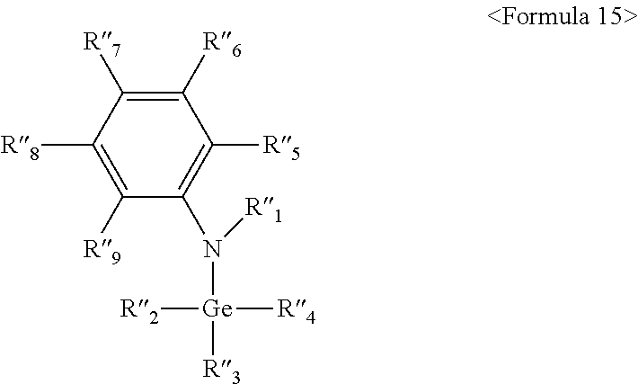
- the organic gallium compound is represented by the following ⁇ Formula 8>:
- the group IV organic compound is a cyclopentadienyl hafnium (IV)-based compound represented by the following ⁇ Formula 23>:
- the precursor composition comprises 1-30 wt % of one compound selected from an organic aluminum compound, an organic gallium compound, and an organic germanium compound.
Landscapes
- Chemical & Material Sciences (AREA)
- Organic Chemistry (AREA)
- Engineering & Computer Science (AREA)
- Materials Engineering (AREA)
- Chemical Kinetics & Catalysis (AREA)
- General Chemical & Material Sciences (AREA)
- Mechanical Engineering (AREA)
- Metallurgy (AREA)
- Inorganic Chemistry (AREA)
- Health & Medical Sciences (AREA)
- Physics & Mathematics (AREA)
- Toxicology (AREA)
- Life Sciences & Earth Sciences (AREA)
- Wood Science & Technology (AREA)
- General Physics & Mathematics (AREA)
- Manufacturing & Machinery (AREA)
- Computer Hardware Design (AREA)
- Microelectronics & Electronic Packaging (AREA)
- Power Engineering (AREA)
- Condensed Matter Physics & Semiconductors (AREA)
- Plasma & Fusion (AREA)
- Electromagnetism (AREA)
- Medicinal Chemistry (AREA)
- Polymers & Plastics (AREA)
- Chemical Vapour Deposition (AREA)
- Formation Of Insulating Films (AREA)
Abstract
Description


Claims (39)


Applications Claiming Priority (6)
| Application Number | Priority Date | Filing Date | Title |
|---|---|---|---|
| KR10-2015-0162796 | 2015-11-19 | ||
| KR1020150162796 | 2015-11-19 | ||
| KR20150162796 | 2015-11-19 | ||
| KR1020160025179A KR20170058820A (en) | 2015-11-19 | 2016-03-02 | Precusor compositions including organo group 4 compounds and method for forming thin film using the same |
| KR10-2016-0025179 | 2016-03-02 | ||
| PCT/KR2016/012456 WO2017086630A1 (en) | 2015-11-19 | 2016-11-01 | Precursor composition containing group iv organic compound and method for forming thin film using same |
Publications (2)
| Publication Number | Publication Date |
|---|---|
| US20180347042A1 US20180347042A1 (en) | 2018-12-06 |
| US10597777B2 true US10597777B2 (en) | 2020-03-24 |
Family
ID=59053673
Family Applications (1)
| Application Number | Title | Priority Date | Filing Date |
|---|---|---|---|
| US15/776,942 Active US10597777B2 (en) | 2015-11-19 | 2016-11-01 | Precursor composition containing group IV organic compound and method for forming thin film using same |
Country Status (4)
| Country | Link |
|---|---|
| US (1) | US10597777B2 (en) |
| JP (1) | JP6705006B2 (en) |
| KR (2) | KR20170058820A (en) |
| CN (1) | CN108603046A (en) |
Families Citing this family (4)
| Publication number | Priority date | Publication date | Assignee | Title |
|---|---|---|---|---|
| KR102333599B1 (en) * | 2019-11-15 | 2021-11-30 | 주식회사 이지티엠 | Method of depositing thin films using protective material |
| KR102224067B1 (en) * | 2020-01-09 | 2021-03-08 | 주식회사 이지티엠 | Method of depositing thin films using protective material |
| WO2021172867A1 (en) * | 2020-02-24 | 2021-09-02 | 주식회사 유피케미칼 | Aluminum precursor compound, production method therefor, and aluminum-containing layer forming method using same |
| KR102365249B1 (en) * | 2020-05-11 | 2022-02-21 | 주식회사 이지티엠 | Precursor compositions including organic silicon amine compound for film deposition, and depositing methods of film using the same |
Citations (6)
| Publication number | Priority date | Publication date | Assignee | Title |
|---|---|---|---|---|
| US20070252244A1 (en) * | 2006-04-28 | 2007-11-01 | Micron Technology, Inc. | Methods of forming material over substrates |
| US20080032465A1 (en) * | 2006-08-03 | 2008-02-07 | Micron Technology, Inc. | Deposition of ZrAION films |
| US20090091003A1 (en) * | 2005-10-19 | 2009-04-09 | Electronics And Telecommunications Research | Insulator undergoing abrupt metal-insulator transition, method of manufacturing the insulator, and device using the insulator |
| US20150110958A1 (en) * | 2014-12-23 | 2015-04-23 | L'Air Liquide, Société Anonyme pour l'Etude et l' Exploitation des Procédés Georges Claude | Germanium- and zirconium-containing compositions for vapor deposition of zirconium-containing films |
| US20170044664A1 (en) * | 2016-10-28 | 2017-02-16 | L'Air Liquide, Société Anonyme pour l'Etude et l'Exploitation des Procédés Georges Claude | Hafnium-containing film forming compositions for vapor deposition of hafnium-containing films |
| US20170117142A1 (en) * | 2014-03-18 | 2017-04-27 | Eugene Technology Materials Co., Ltd. | Organic Germanium Amine Compound and Method for Depositing Thin Film Using the Same |
Family Cites Families (10)
| Publication number | Priority date | Publication date | Assignee | Title |
|---|---|---|---|---|
| DE3907579A1 (en) * | 1989-03-09 | 1990-09-13 | Merck Patent Gmbh | USE OF METAL ORGANIC COMPOUNDS FOR DEPOSITION OF THIN FILMS FROM THE GAS PHASE |
| JPH07300398A (en) * | 1994-05-06 | 1995-11-14 | Sumitomo Chem Co Ltd | Method for synthesizing IIIb-Vb group compound |
| US6984591B1 (en) * | 2000-04-20 | 2006-01-10 | International Business Machines Corporation | Precursor source mixtures |
| US7332618B2 (en) * | 2004-09-28 | 2008-02-19 | Praxair Technology, Inc. | Organometallic precursor compounds |
| EP2029790A1 (en) * | 2006-06-02 | 2009-03-04 | L'AIR LIQUIDE, Société Anonyme pour l'Etude et l'Exploitation des Procédés Georges Claude | Method of forming high-k dielectric films based on novel titanium, zirconium, and hafnium precursors and their use for semiconductor manufacturing |
| JP5957017B2 (en) * | 2011-03-15 | 2016-07-27 | メカロニックス シーオー. エルティディ.Mecharonics Co. Ltd. | Novel group 4B organometallic compound and method for producing the same |
| US9082702B2 (en) * | 2012-02-27 | 2015-07-14 | Applied Materials, Inc. | Atomic layer deposition methods for metal gate electrodes |
| JP6378307B2 (en) * | 2013-03-11 | 2018-08-22 | ユニバーシティ オブ フロリダ リサーチ ファンデーション インコーポレーティッド | Substances and methods for improving lung function and for preventing and / or treating radiation-induced lung complications |
| KR102008445B1 (en) * | 2014-02-26 | 2019-08-08 | 주식회사 유진테크 머티리얼즈 | Precursor compositions for forming zirconium-containing film and method of forming zirconium-containing film using them as precursors |
| RU2016135995A (en) * | 2014-03-04 | 2018-04-04 | Пикосан Ой | ATOMIC-LAYER DEPOSITION OF GERMANY OR GERMANY OXIDE |
-
2016
- 2016-03-02 KR KR1020160025179A patent/KR20170058820A/en not_active Ceased
- 2016-11-01 US US15/776,942 patent/US10597777B2/en active Active
- 2016-11-01 CN CN201680067477.9A patent/CN108603046A/en active Pending
- 2016-11-01 JP JP2018545788A patent/JP6705006B2/en active Active
-
2018
- 2018-10-29 KR KR1020180130163A patent/KR20180132568A/en not_active Ceased
Patent Citations (6)
| Publication number | Priority date | Publication date | Assignee | Title |
|---|---|---|---|---|
| US20090091003A1 (en) * | 2005-10-19 | 2009-04-09 | Electronics And Telecommunications Research | Insulator undergoing abrupt metal-insulator transition, method of manufacturing the insulator, and device using the insulator |
| US20070252244A1 (en) * | 2006-04-28 | 2007-11-01 | Micron Technology, Inc. | Methods of forming material over substrates |
| US20080032465A1 (en) * | 2006-08-03 | 2008-02-07 | Micron Technology, Inc. | Deposition of ZrAION films |
| US20170117142A1 (en) * | 2014-03-18 | 2017-04-27 | Eugene Technology Materials Co., Ltd. | Organic Germanium Amine Compound and Method for Depositing Thin Film Using the Same |
| US20150110958A1 (en) * | 2014-12-23 | 2015-04-23 | L'Air Liquide, Société Anonyme pour l'Etude et l' Exploitation des Procédés Georges Claude | Germanium- and zirconium-containing compositions for vapor deposition of zirconium-containing films |
| US20170044664A1 (en) * | 2016-10-28 | 2017-02-16 | L'Air Liquide, Société Anonyme pour l'Etude et l'Exploitation des Procédés Georges Claude | Hafnium-containing film forming compositions for vapor deposition of hafnium-containing films |
Also Published As
| Publication number | Publication date |
|---|---|
| KR20170058820A (en) | 2017-05-29 |
| CN108603046A (en) | 2018-09-28 |
| US20180347042A1 (en) | 2018-12-06 |
| KR20180132568A (en) | 2018-12-12 |
| JP2019504509A (en) | 2019-02-14 |
| JP6705006B2 (en) | 2020-06-03 |
Similar Documents
| Publication | Publication Date | Title |
|---|---|---|
| JP7230126B2 (en) | A novel formulation for the deposition of silicon-doped hafnium oxide as a ferroelectric material. | |
| US12247289B2 (en) | Method for forming thin film using surface protection material | |
| US9443736B2 (en) | Silylene compositions and methods of use thereof | |
| CN100511594C (en) | Hafnium-aluminum oxide dielectric films | |
| US10597777B2 (en) | Precursor composition containing group IV organic compound and method for forming thin film using same | |
| CN100422383C (en) | Systems and methods for forming metal oxides using alcohols | |
| US9828402B2 (en) | Film-forming composition and method for fabricating film by using the same | |
| CN102082087B (en) | Comprise semiconductor device and the manufacture method thereof of carbon-containing electrode | |
| US20060264066A1 (en) | Multilayer multicomponent high-k films and methods for depositing the same | |
| CN106367730A (en) | Methods for depositing group 13 metal or metalloid nitride films | |
| US20100270508A1 (en) | Zirconium precursors useful in atomic layer deposition of zirconium-containing films | |
| JP2004260168A (en) | Atomic layer deposition of nanolaminate films | |
| US20230057512A1 (en) | Method for forming thin film using surface protection material | |
| JP2022548037A (en) | Formulation for deposition of silicon-doped hafnium oxide | |
| US20210222294A1 (en) | Metal triamine compound, method for preparing the same, and composition for depositing metal-containing thin film including the same | |
| US12252781B2 (en) | Area-selective method for forming thin film by using nuclear growth retardation | |
| US20220112600A1 (en) | Method of depositing thin films using protective material | |
| KR20220090731A (en) | Precursor for film deposition, deposition method of film and semiconductor device of the same | |
| JP6272033B2 (en) | Method for producing silicon oxide or silicon oxynitride thin film by atomic layer deposition | |
| KR20210155106A (en) | Lanthanide precursor and lanthanide-containing film using the same and deposition method of the same and semiconductor device comprising the same | |
| KR20090014870A (en) | Method for forming DXYSC3 film by ALD, lamination structure of semiconductor thin film including DXYSC3 film and its formation method | |
| KR101021875B1 (en) | Metal Organic Chemical Vapor Deposition of Hafnium Film with Improved Uniformity | |
| US20060189055A1 (en) | Method of forming a composite layer, method of manufacturing a gate structure by using the method of forming the composite layer and method of manufacturing a capacitor by using the method of forming the composite layer | |
| US20250353865A1 (en) | Amine adducts of group 2 metallocene precursors for depositon of group 2 metal films | |
| KR20110007262A (en) | Metal-organic Chemical Vapor Deposition of Hafnium Film with Improved Uniformity |
Legal Events
| Date | Code | Title | Description |
|---|---|---|---|
| AS | Assignment |
Owner name: EUGENETECH MATERIALS CO., LTD., KOREA, REPUBLIC OF Free format text: ASSIGNMENT OF ASSIGNORS INTEREST;ASSIGNORS:LEE, GEUN-SU;LEE, YEONG-MIN;REEL/FRAME:045834/0153 Effective date: 20180514 |
|
| FEPP | Fee payment procedure |
Free format text: ENTITY STATUS SET TO UNDISCOUNTED (ORIGINAL EVENT CODE: BIG.); ENTITY STATUS OF PATENT OWNER: SMALL ENTITY |
|
| FEPP | Fee payment procedure |
Free format text: ENTITY STATUS SET TO SMALL (ORIGINAL EVENT CODE: SMAL); ENTITY STATUS OF PATENT OWNER: SMALL ENTITY |
|
| STPP | Information on status: patent application and granting procedure in general |
Free format text: DOCKETED NEW CASE - READY FOR EXAMINATION |
|
| STPP | Information on status: patent application and granting procedure in general |
Free format text: NON FINAL ACTION MAILED |
|
| STPP | Information on status: patent application and granting procedure in general |
Free format text: RESPONSE TO NON-FINAL OFFICE ACTION ENTERED AND FORWARDED TO EXAMINER |
|
| STPP | Information on status: patent application and granting procedure in general |
Free format text: NOTICE OF ALLOWANCE MAILED -- APPLICATION RECEIVED IN OFFICE OF PUBLICATIONS |
|
| STPP | Information on status: patent application and granting procedure in general |
Free format text: PUBLICATIONS -- ISSUE FEE PAYMENT VERIFIED |
|
| STCF | Information on status: patent grant |
Free format text: PATENTED CASE |
|
| MAFP | Maintenance fee payment |
Free format text: PAYMENT OF MAINTENANCE FEE, 4TH YR, SMALL ENTITY (ORIGINAL EVENT CODE: M2551); ENTITY STATUS OF PATENT OWNER: SMALL ENTITY Year of fee payment: 4 |