US10595822B2 - Ultrasonic-wave probe, ultrasonic-wave diagnosis apparatus, and test method of ultrasonic-wave probe - Google Patents
Ultrasonic-wave probe, ultrasonic-wave diagnosis apparatus, and test method of ultrasonic-wave probe Download PDFInfo
- Publication number
- US10595822B2 US10595822B2 US15/553,197 US201615553197A US10595822B2 US 10595822 B2 US10595822 B2 US 10595822B2 US 201615553197 A US201615553197 A US 201615553197A US 10595822 B2 US10595822 B2 US 10595822B2
- Authority
- US
- United States
- Prior art keywords
- transmission
- reception
- voltage
- circuit
- ultrasonic
- Prior art date
- Legal status (The legal status is an assumption and is not a legal conclusion. Google has not performed a legal analysis and makes no representation as to the accuracy of the status listed.)
- Active, expires
Links
Images


Classifications
-
- G—PHYSICS
- G01—MEASURING; TESTING
- G01R—MEASURING ELECTRIC VARIABLES; MEASURING MAGNETIC VARIABLES
- G01R31/00—Arrangements for testing electric properties; Arrangements for locating electric faults; Arrangements for electrical testing characterised by what is being tested not provided for elsewhere
- G01R31/28—Testing of electronic circuits, e.g. by signal tracer
- G01R31/317—Testing of digital circuits
- G01R31/31712—Input or output aspects
- G01R31/31716—Testing of input or output with loop-back
-
- A—HUMAN NECESSITIES
- A61—MEDICAL OR VETERINARY SCIENCE; HYGIENE
- A61B—DIAGNOSIS; SURGERY; IDENTIFICATION
- A61B8/00—Diagnosis using ultrasonic, sonic or infrasonic waves
- A61B8/44—Constructional features of the ultrasonic, sonic or infrasonic diagnostic device
- A61B8/4444—Constructional features of the ultrasonic, sonic or infrasonic diagnostic device related to the probe
-
- A—HUMAN NECESSITIES
- A61—MEDICAL OR VETERINARY SCIENCE; HYGIENE
- A61B—DIAGNOSIS; SURGERY; IDENTIFICATION
- A61B8/00—Diagnosis using ultrasonic, sonic or infrasonic waves
- A61B8/44—Constructional features of the ultrasonic, sonic or infrasonic diagnostic device
- A61B8/4483—Constructional features of the ultrasonic, sonic or infrasonic diagnostic device characterised by features of the ultrasound transducer
- A61B8/4494—Constructional features of the ultrasonic, sonic or infrasonic diagnostic device characterised by features of the ultrasound transducer characterised by the arrangement of the transducer elements
-
- A—HUMAN NECESSITIES
- A61—MEDICAL OR VETERINARY SCIENCE; HYGIENE
- A61B—DIAGNOSIS; SURGERY; IDENTIFICATION
- A61B8/00—Diagnosis using ultrasonic, sonic or infrasonic waves
- A61B8/58—Testing, adjusting or calibrating the diagnostic device
-
- H—ELECTRICITY
- H04—ELECTRIC COMMUNICATION TECHNIQUE
- H04B—TRANSMISSION
- H04B17/00—Monitoring; Testing
- H04B17/10—Monitoring; Testing of transmitters
- H04B17/15—Performance testing
-
- H—ELECTRICITY
- H04—ELECTRIC COMMUNICATION TECHNIQUE
- H04B—TRANSMISSION
- H04B17/00—Monitoring; Testing
- H04B17/20—Monitoring; Testing of receivers
- H04B17/29—Performance testing
Definitions
- the present invention relates to an operation method of a reception/transmission separation switch for separating and protecting a reception circuit, which is formed by a low-voltage device, from a high-voltage signal output from a transmission circuit, which is formed by a high-withstand-voltage device, the switch mounted on an ultrasonic-wave probe, which is a constituent element of an ultrasonic-wave diagnosis apparatus.
- the present invention particularly relates to the techniques to realize a test method to test the transmission circuit and the reception circuit for each oscillator by using a signal subjected to loopback from the transmission circuit to the reception circuit in the ultrasonic-wave probe.
- An ultrasonic-wave diagnosis apparatus is a non-invasive and highly safe medical diagnostic device for the human body and has a small apparatus scale compared with other medical image diagnosis apparatuses such as an X-ray diagnosis apparatus and a magnetic resonance imaging (MRI) apparatus.
- MRI magnetic resonance imaging
- the apparatus is capable of displaying in real time the state of motion of an examination target such as pulsation of the heart or movement of the fetus by simple operation of simply causing an ultrasonic-wave probe to abut from the body surface, the apparatus plays an important role in the medical care of today.
- ultrasonic waves are transmitted into a subject by supplying high-voltage drive signals to each of a plurality of oscillators incorporated in the ultrasonic-wave probe.
- the reflected waves of ultrasonic waves generated by differences in acoustic impedance of living tissues in the subject are received by each of a plurality of oscillator elements, and images are generated based on the reflected waves received by the ultrasonic-wave probe.
- a transmission circuit which supplies high-voltage drive signals to each of the oscillators built in the ultrasonic-wave probe is composed of a high-withstand-voltage device so that high-voltage signals of Vpeak to peak of several tens to a hundred and several tens can be generated.
- a device with a structure that relaxes the electric field intensity between a drain and a gate such as laterally diffused MOS (LDMOS) is used for a high-withstand-voltage metal-oxide-semiconductor field effect transistor (MOSFET), and it requires an extremely large area to ensure a drift region between the drain and the gate. Therefore, when the transmission circuit is to be realized as an integrated circuit (IC: Integrated Circuit) on silicon, a large area is required.
- IC integrated Circuit
- the amplitude of the reception signal subjected to acoustic-electric conversion by each oscillator is extremely small, and the reception circuit for subjecting this to amplification and signal processing is composed of a low-voltage device for the sake of low noise, low power consumption and small area.
- each of the oscillators in the ultrasonic-wave probe is a transducer in which the same element carries out both of electric-acoustic and acoustic-electric, and both of the transmission circuit for supplying a high voltage to the same element and the reception circuit for receiving minute reception signals are connected.
- a switch is normally inserted between the oscillator and the reception circuit so that the reception circuit composed of the low-voltage device is not electrically destroyed when the transmission circuit supplies the high-voltage drive signal to the oscillator.
- This switch is referred to as a transmission/reception separation switch.
- the transmission/reception separation switch becomes a switch-off state in a case of transmission to separate the reception circuit from the high-voltage drive signal generated by the transmission circuit and prevent electrical destruction. It becomes a switch-on state in a case of reception and has a role of causing minute reception signals from the oscillator to pass through with low loss. From the above roles, the transmission/reception separation switch is required to have electrical characteristics that can withstand high-voltage signals, and it is necessary to construct it with a high-withstand-voltage device.
- an ultrasonic-wave diagnosis apparatus capable of obtaining three-dimensional stereoscopic images has been developed, and examination efficiency can be improved by obtaining a tomographic image by specifying an arbitrary cross section from the three-dimensional stereoscopic image.
- the oscillators in the ultrasonic-wave probe have to be changed from a conventional one-dimensional arrangement to a two-dimensional arrangement, and the number of the oscillators is increased to the second power compared with a conventional ultrasonic-wave probe.
- the functions of transmission/reception and phase-adjustment addition are realized as a beamformer IC, transmission/reception circuits are disposed respectively for the oscillators in the IC to prepare pads electrically connected to the oscillators by one-to-one correspondence, and peripheral pads for transmitting outputs after the phase-adjustment addition to the main-body device are prepared separately from them.
- FIG. 6 is a perspective view showing an example of a beamformer IC.
- 100 is a silicon wafer or an IC chip
- 200 is an oscillator connecting pad connected to an oscillator (not shown)
- 300 is a peripheral pad connected to a main-body-device interface, and the like.
- the signal amplitude input to the subsequent reception circuit has to be limited by operating the transmission/reception separation switch in a third state different from a normal transmission state and from a normal reception state, preventing withstand voltage violation in the transmission/reception separation switch, and attenuating the signal looped back therein by the transmission/reception separation switch.
- FIG. 14 is FIG. 7 of PTL 1 re-illustrated from the viewpoint of the inventors in order to understand problems of the present invention.
- FIG. 14 relates to a transmission/reception separation switch using a MOS on a triple well.
- “ 1401 ” is a processor for transmitting/receiving signals
- “ 1402 ” is a transmission circuit
- “ 1403 ” is a power amplifier for transmission.
- RFIO is a terminal for transmission and reception.
- “ 1404 ” and “ 1405 ” are transmission/reception separation switches
- “ 1406 ” is an attenuator
- “ 1407 ” and “ 1408 ” are amplifiers
- “ 1409 ” is a reception circuit.
- normal reception is an operation of amplifying the output of the transmission/reception separation switch 1404 having a small loss by a low noise amplifier (LNA: Low Noise Amplifier) 0 ( 1407 ); and, in internal-signal loopback calibration, reception is carried out by the signal path of LNA 1 ( 1408 ) passed through the attenuator 1406 subsequent to the transmission/reception separation switch 1405 , thereby avoiding destruction of the reception circuit 1409 .
- LNA Low Noise Amplifier
- a low noise receiver can be formed by using a low-loss switch in the case of reception; and, in the case of internal-signal loopback calibration, the signal amplitude can be limited by the attenuator to prevent destruction of the reception circuit.
- the signal path which is amplified by LNA 0 also in the case of internal-signal loopback has to be selected. Even if the operation of LNA 1 is tested by the signal path amplified by LNA 1 , it does not mean that LNA 0 has been tested. Moreover, if an attenuator is disposed in front of LNA 0 so that LNA 0 is not destroyed and an internal-signal loopback test is to be carried out, the attenuator is inserted in series in the signal path. Therefore, increase in the loss and the noise index in a normal receiving operation are inevitable. Furthermore, in the configuration of FIG. 14 , it is necessary to prepare circuits for two paths for normal reception and for internal-signal loopback, and there is also a problem that the circuit area is increased.
- a switch-off state is obtained in a case of transmission, wherein a reception circuit is separated from a high-voltage drive signal generated by a transmission circuit to prevent electric breakdown; and a switch-on state is obtained in a case of reception, wherein a minute reception signal from an oscillator is caused to pass through with low loss in a transmission/reception separation switch circuit; wherein, in an internal-signal loopback test from the transmission circuit to the reception circuit, a gate-source voltage Vgs of high-withstand-voltage MOS constituting a switch is lowered than that in a case of normal reception. More preferably, a low-voltage MOS is connected between a switch output and 0-V GND or a predetermined power source and is turned on in the internal-signal loopback test.
- the transmission/reception separation switch is provided with a function of signal attenuation without providing an attenuator on a reception signal path.
- a signal path of normal reception and a signal path in a case of internal-signal loopback like PTL 1
- the operations of the transmission/reception circuit per se, which carries out actual transmission/reception operations can be tested by internal-signal loopback.
- the gate-source voltage Vgs of the MOS constituting the transmission/reception separation switch is changed in the case of reception and in the case of internal-signal loopback test.
- Vgs is biased to a vicinity of a maximum withstand voltage to realize the reception circuit with a low on-resistance, in other words, low loss and low noise, and, on the other hand, the withstand voltage is ensured so as not to destroy the device in the internal-signal loopback test, wherein high reception performance and high testability are both enabled.
- Another aspect of the present invention is an ultrasonic-wave probe having an oscillator, a transmission circuit connected to the oscillator, a reception circuit connected to the oscillator, and a transmission/reception separation switch disposed between the oscillator and the reception circuit.
- the transmission/reception separation switch has two transistor elements, and gates and sources of the two transistor elements are mutually connected.
- a gate-potential step-down circuit for lowering the voltage Vgs between the common gate and the common source of the two transistors is provided.
- a gate potential of the transistor is stepped down to cause the test signal to pass through while ensuring the voltage Vgs between the common gate and the common source, the voltage which does not violate a gate-source withstand voltage of the transistor.
- a test mode can be realized in addition to a transmission/reception mode.
- an output-side transistor is connected to a switch output of the transmission/reception separation switch, and a connection destination of the output-side transistor is GND of 0 V or a power source corresponding to a center voltage of a signal applied to an input in a switch-on state. Then, by short-circuiting the switch output to GND or to the power source corresponding to the center voltage via the output-side transistor, the input signal voltage of the transmission/reception separation switch is divided by the on-resistance of the transmission-reception separation switch and the on-resistance of the output-side transistor, and the signal amplitude thereof is attenuated.
- Another aspect of the present invention is an ultrasonic-wave diagnosis apparatus having a sub array, an adder circuit configured to add an output from the sub array, and a main-body device configured to process an output from the adder circuit.
- the sub array includes a plurality of oscillator channels; and each of the oscillator channels has an oscillator, a transmission circuit connected to the oscillator, a reception circuit connected to the oscillator, and a transmission/reception separation switch.
- the transmission/reception separation switch has a transistor as a switching element and has a potential control circuit for controlling a gate-source voltage Vgs of the transistor.
- the switch has: a transmission mode to cause the transmission/reception separation switch to be in an off-state in a case of transmission in which a signal from the transmission circuit is input to the oscillator; a reception mode to cause the transmission/reception separation switch to be in an on-state in a case of reception in which a signal is input from the oscillator to the reception circuit; and a test mode to set the gate-source voltage Vgs of the transistor to a potential different from the potential in the transmission mode and the potential in the reception mode by the potential control circuit.
- Another aspect of the present invention is a test method of an ultrasonic-wave probe having an oscillator, a transmission circuit connected to the oscillator, a reception circuit connected to the oscillator, and a transmission/reception separation switch disposed between the oscillator and the reception circuit.
- the transmission/reception separation switch has two transistor elements and is configured to mutually connect a gate and a source of the two transistor elements; and the switch has: a transmission mode to cause the transmission/reception separation switch to be in an off-state in a case of transmission in which the oscillator is driven by the transmission circuit; a reception mode to cause the transmission/reception separation switch to be in an on-state in a case of reception in which a signal from the oscillator is input to the reception circuit; and a test mode to set the voltage Vgs between the common gate and the common source of the two transistors at the middle between the voltage in the transmission mode and the voltage in the reception mode.
- the internal-signal loopback test method in which the signal is attenuated and output while ensuring the withstand voltage in the transmission/reception separation switch so that the subsequent low-voltage reception circuit is not destroyed can be realized.
- FIG. 1 is a circuit diagram showing a circuit configuration for generating Vgs of a high-withstand-voltage NMOS by resistance voltage dividing as an example of an embodiment of the present invention.
- FIG. 2 is a circuit diagram showing a circuit configuration for generating Vgs of the high-withstand-voltage NMOS with serially-connected forward diodes as a first embodiment instead of the resistance voltage dividing of FIG. 1 .
- FIG. 3 is a circuit diagram showing a circuit configuration for generating Vgs of a high-withstand-voltage NMOS by series connection of diode-connected NMOSs connecting drains and gates to each other as a second embodiment, in place of the resistance voltage dividing of FIG. 1 .
- FIG. 4 is a circuit diagram showing a circuit configuration in which an ideal switch in the embodiment of FIG. 3 is expressed by actual elements.
- FIG. 5 is a table diagram of a truth-value table expressing relations between operation modes and control signals of the circuit configuration by the actual elements of FIG. 4 .
- FIG. 6 is a perspective view showing a test configuration of an IC in a state of a silicon wafer or a chip after dicing.
- FIG. 7 is a block diagram showing a system configuration example of an ultrasonic-wave diagnosis apparatus to which the present invention is applied.
- FIG. 8 is a block diagram showing a sub array configuration example of an IC in the ultrasonic-wave probe to which the present invention is applied.
- FIG. 9 is a block diagram showing a configuration example including a judge device for judging a result of an internal-signal loopback test in the IC in the sub array of the IC in the ultrasonic-wave probe to which the present invention is applied.
- FIG. 10 is a timing chart showing operation principles of the judge device for judging the test result according to the frequency of an internal loopback signal.
- FIG. 11 is a circuit diagram showing a circuit configuration of the judge device for judging the test result according to the frequency of the internal loopback signal.
- FIG. 12 is a timing chart showing operation principles of the judge device for judging both of the frequency and amplitude of the internal loopback signal.
- FIG. 13 is a block diagram showing a circuit configuration of the judge device to judge both of the frequency and amplitude of the internal loopback signal.
- FIG. 14 is a block diagram re-illustrating FIG. 7 of PTL 1 from the viewpoint of the inventors.
- FIG. 15 is a block diagram showing a sub array configuration example of the IC in the ultrasonic-wave probe to which the present invention is applied.
- FIG. 1 shows a configuration of an embodiment of the present invention.
- a basic switching circuit with two high-withstand-voltage NMOSs N-channel enhancement type metal-oxide-semiconductor field-effect transistors (MOSFETs)) in which a gate and a source of MN 0 and MN 1 in FIG. 1 are connected to each other in series is widely known as a publicly known circuit.
- MOSFETs N-channel enhancement type metal-oxide-semiconductor field-effect transistors
- a potential is determined outside the configuration of FIG. 1 , for example, by connecting a switch input SWIN and a switch output SWOUT of FIG. 1 to GND of 0 V via a resistance.
- MN 0 and MN 1 in FIG. 1 are high-withstand-voltage MOSs.
- a device with a structure that relaxes the electric field intensity between a drain and a gate such as LDMOS
- LDMOS has a structure in which the source and the drain are asymmetric, and the source and the bulk are connected.
- the structure between the drain and the gate and between the drain and the source can withstand a high voltage such as several tens V or 100 V or more, but only a low voltage such as 5 V can be applied between the gate and the source.
- the line on the left side of the symbol of MN 0 is thickened, which means that the left side is the drain in terms of structure and there is a drift region for relaxing electric fields.
- MN 2 is a transistor connected to a switch output of a transmission/reception separation switch. This transistor may be a low-voltage transistor.
- a connection destination of the transistor MN 2 is GND of 0 V or a power source corresponding to a center voltage of a signal applied to the input in a switch-on state.
- the input, signal voltage of the transmission/reception separation switch is divided by the on-resistance of the switch and the on resistance of the transistor MN 2 , and the signal amplitude thereof is attenuated.
- VCG Vdd ⁇ R ⁇ ⁇ 1 R ⁇ ⁇ 0 + R ⁇ ⁇ 1 [ Mathematical ⁇ ⁇ Expression ⁇ ⁇ 1 ]
- This VCG is applied as Vgs of MN 0 and MN 1 , and MN 0 and MN 1 are turned on with a lower voltage than that of reception and with a high resistance. This state is assigned to an internal-signal loopback test mode.
- Vgs becomes low since it is determined by the voltage division ratio according to R 0 and R 1 of Vdd, wherein ⁇ 2 V from the transmission circuit can be received by appropriately taking the ratio of R 0 and R 1 .
- R 0 R 1
- 3.5 V which is half of 7 V
- VOUT VIN ⁇ RMN ⁇ ⁇ 2 RMN ⁇ ⁇ 0 + RMN ⁇ ⁇ 1 + RMN ⁇ ⁇ 2 [ Mathematical ⁇ ⁇ Expression ⁇ ⁇ 2 ]
- Vgs of MN 0 and MN 1 is lower than that in the case of reception, and, since on-resistances RMN 0 and RMN 1 are higher, the output amplitude thereof can be further reduced by increasing the denominator of the above described expression.
- the transmission/reception separation switch per se is used as an attenuator, there is no need to prepare an attenuator separately from the transmission/reception separation switch like PTL 1. Furthermore, since the same signal path is used in the case of reception and in the case of internal-signal loopback test, a test can be carried out for the reception circuit per se used for the actual receiving operation. In the case of transmission, SW 0 is turned off, SW 1 is turned on, and MN 0 and MN 1 are turned off, thereby turning off the transmission/reception separation switch.
- FIG. 2 shows an embodiment of the transmission/reception separation switch according to the present invention.
- Vgs of MN 0 and MN 1 is generated by resistance voltage division by the resistance voltage division of R 0 and R 1 . Since current flows from Vdd to R 0 and R 1 at this time, for example, in order to suppress the power consumption to the order of ⁇ W, it is necessary to set R 0 and R 1 to high resistances of the order of M ⁇ ; and, although it depends on the sheet resistance of the resistance type prepared in a semiconductor process used, there is a concern that the area of the resistance increases.
- forward diodes D 0 , D 1 , D 2 , and D 3 are used instead of R 0 in FIG. 1 .
- the internal-signal loopback test mode is obtained by turning SW 0 on, SW 1 off, and SW 2 off, the forward voltage of the diodes at this point is Vf, and the potential of the common gate CG becomes (Mathematical Expression 3).
- VCG Vdd ⁇ 4 ⁇ Vf [Mathematical Expression 3]
- VCG falls from Vdd by Vf of the diodes in four stages.
- the number of serial stages of the forward diodes may be adjusted according to the required VCG. Since a current is passed through the diodes to generate Vf, a resistance R 0 or a current source is required between CG and CS.
- a circuit area can be reduced than in the configuration of FIG. 1 .
- FIG. 3 shows an embodiment of the transmission/reception separation switch according to the present invention.
- the forward diodes are used to lower the potential VCG of the common gate CG from Vdd.
- diodes usable in the forward direction are designed on the assumption that a large current for rectification is to flow therethrough, and the area thereof may be large.
- diode-connected MGSs in each of which a drain and a gate are connected to each other are used instead of the diodes of the first embodiment.
- the internal-signal loopback test mode is obtained by turning SW 0 on, SW 1 off, and SW 2 off, gate-source voltages of MN 3 , MN 4 , MR 5 , and MN 6 at this point are Vgsd, and the potential of the common gate CG becomes (Mathematical Expression 4).
- VCG Vdd ⁇ 4 ⁇ Vgsd [Mathematical Expression 4]
- VCG falls from Vdd by Vgsd of the diode-connected MOSs in four stages.
- the number of serial stages of the diode-connected MOSs may be adjusted according to the required VCG. Since a current is passed through the diode-connected MOSs to generate Vgsd, a resistance R 0 or a current source is required between CG and CS.
- resistive elements with high sheet resistances or diodes with small areas that can be used in the forward direction are not prepared, there is a higher possibility in the present embodiment that the circuit area can be reduced than in the configuration of FIG. 1 or the first embodiment of FIG. 2 .
- FIG. 4 shows a different embodiment of the transmission/reception separation switch according to the present invention.
- the elements expressed as ideal switches in FIGS. 1, 2, and 3 are realized by actual MOSs.
- SW 0 in FIG. 3 is replaced by MP 0 in FIG. 4
- SW 1 in FIG. 3 is replaced by SHT in FIG. 4
- SW 2 in FIG. 3 is replaced by MN 7 and MP 1 in FIG. 4 .
- the transmission circuit In a case of transmission, the transmission circuit outputs high-voltage pulses of positive voltages or negative voltages; wherein, in a case in which a negative voltage is output, SWIN becomes a negative voltage, the drain in the structure of MN 0 electrically serves as a source, and MN 0 is turned on to be low to lower CS to a negative voltage. Therefore, CS and CG swing between the negative voltage and 0 V in the case of transmission. Therefore, a PMOS with a high withstand voltage has to be used as MP 0 for switching the operations of transmission and reception. Also, the circuit connected to the source side of MP 0 can be formed by using a low-voltage MOS since it is protected by MP 0 .
- SHT in FIG. 4 is a shunt circuit and operates as a switch for turning off MN 0 and MN 1 in the case of transmission.
- MN 8 is normally off since a gate and a source thereof are connected to each other via R 1 .
- SWIN and CS are driven to negative voltages, the voltage between CG and CS increases at a certain slew rate or higher, C 1 follows this to turn on MN 8 and short-circuit CG and CS.
- FIG. 5 is a truth-value table related to each mode state of the second embodiment of FIG. 4 .
- Tx/Rx is a transmission/reception switching signal
- BYP is a bypass signal of a gate step-down circuit
- VSSHT is a gate control signal of a low-voltage NMOS gate control signal which short-circuits the output to GND.
- transmission in other words, when Tx/Rx is at a low level and BYP and VSSHT are at a high level, an inverter INV 1 outputs a low level, this passes through a bypass switch of MN 7 and MP 1 and gives 0 V to the source of MP 0 , and MP 0 is turned off.
- MN 0 and MN 1 constituting the switch are subjected to gate-source short-circuiting constantly by R 0 and transiently by SHT and become an off-state.
- MN 2 is turned on to suppress AC signal leakage to the output due to parasitic capacity coupling in the case of transmission and improve isolation performance.
- the inverter INV 1 In the case of reception, in other words, when Tx/Rx and BYP are at a high level and VSSHT is at a low level, the inverter INV 1 outputs a high level, this passes through the bypass switch of MN 7 and MP 1 and gives Vdd to the source of MP 0 , and MP 0 is turned on, Vdd is applied as the gate-source voltage Vgs of MN 0 and MN 1 constituting the switch, high Vgs is applied thereto, and it is turned on as the transmission/reception separation switch with a low on-resistance. MN 2 is turned off so that there is no loss of the received signal.
- the gate-source voltage Vgs of MN 0 and MN 1 constituting the switch is lower than that in the case of reception, and MN 0 and MN 1 are turned on with high resistances. Since MN 2 is on, the internal loopback signal input from SWIN can be subjected to voltage-division and attenuated by MN 0 , MN 1 , and MN 2 and be output to the subsequent low-voltage reception circuit with a small amplitude.
- FIG. 6 shows a test configuration of a beamformer IC in an ultrasonic-wave probe having 2-dimensional array oscillators applied to the present invention in a state of a silicon wafer or in a state of an IC chip after dicing.
- the number of pads 200 connected to the oscillators (not shown) varies from several thousands to over ten thousand or more in a chip 100 , and the number of the pads is too large. Therefore, it is difficult to cause probes to contact all of them to test transmission/reception circuits in the IC one channel at a time by a tester.
- test results can be monitored by the tester or the main-body device, and defective products of the IC can be subjected to screening.
- FIG. 7 shows the ultrasonic-wave probe having the 2-dimensional array oscillators for 3-dimensional image pickup and a system configuration to which the present invention is applied.
- transmission/reception circuits 702 are disposed respectively for the oscillators 701 , and reception outputs are added by an adder circuit 703 and transmitted to an analog front end (AFE) 711 of the main-body device 710 .
- AFE analog front end
- a grouping unit of oscillator channels to be subjected to addition is referred to as a sub array 707 .
- the transmission/reception circuits 702 , the adder circuit 703 , a sub-array-control logic circuit 704 , and the like are formed by a single chip as shown in FIG. 6 .
- the oscillator connecting pad 200 shown in FIG. 6 is connected to the oscillators 701 .
- a processor 712 in the main-body device 710 transmits control signals to a control logic circuit 705 of the IC in the ultrasonic-wave probe, and the IC control logic circuit 705 carries out control such as switching of transmission/reception in response thereto.
- the scale of the IC control logic circuit and the number of control signals in the IC can be reduced by controlling transmission/reception switching related to the control of the transmission/reception separation switch collectively by each sub array.
- FIG. 7 it is possible to dispose sub-array-control logic circuits respectively for the sub arrays, hierarchize control, and independently control each of the transmission/reception circuits from the sub-array-control logic circuit by granularity.
- the IC control logic circuit 705 includes a waveform memory 706 which stores the waveform data transmitted by the pulsar.
- FIG. 8 shows details of the configuration in the sub array 707 .
- the transmission/reception circuit 702 for each oscillator includes a transmission circuit 7021 which is formed of a high-withstand-voltage MOS and generates a high-voltage signal to drive the oscillator 701 , a transmission/reception separation switch 7022 according to the present invention, a reception analog front end 7023 of a low voltage system, and a minute delay circuit 7024 which delays transmission signals to carry out beam forming and delays reception signals to carry out phase adjustment.
- the reception signals, which have undergone phase adjustment by the minute delay circuit 7024 are subjected to addition by the adder circuit 703 and transmitted to the main-body device 710 .
- a plurality of sets of the oscillators 701 and transmission/reception circuits 702 are present.
- One oscillator and a transmission/reception circuit connected thereto constitute one oscillator channel.
- the minute delay circuit 7024 is used for ultrasonic-wave beam forming by focusing in the case of transmission and is used for phase-adjustment addition in the case of reception.
- the same circuit is used for both transmission and reception, since the transmission circuit and the reception circuit are required to operate at the same time in the internal-signal loopback test, the operation in the internal-signal loopback test of the minute delay circuit has to be assigned to either operation or reception.
- the minute delay circuit 7024 is carrying out a reception operation in the internal-signal loopback test. In the case of normal transmission, a waveform signal S is input to the minute delay circuit, is delayed by the minute delay circuit, and is transmitted by the transmission circuit 7021 as a delayed waveform signal DS.
- a loopback-test waveform signal TS from the sub-array-control logic circuit 704 is selected by a selector 7025 provided before the transmission circuit and is input to the transmission circuit 7021 .
- the transmitted signal is input to the transmission/reception separation switch 7022 in the internal-signal loopback test mode, is attenuated to have a small amplitude, and is input to the reception AFE 7023 .
- the signal is delayed by the minute delay circuit 7024 , is added to the signals of the other oscillator channels, and is output from the sub array 707 . No signal is input to the oscillator channels which are not test targets of the sub array so that they output no signals.
- the output from the transmission/reception circuit of the oscillator channel serving as a test target can be obtained as an output of the adder circuit. Therefore, the single channel of the oscillator can be tested. More specifically, the transmission circuit 7021 , the reception circuit 7023 , and the minute delay circuit 7024 can be tested. Note that C 1 is a control signal of the transmission/reception separation switch 7022 , and C 2 is a control signal of the selector 7025 .
- a B-mode in which the intensity of reflected signals is converted into luminance to form images and a mode in which Doppler signals are expressed by colors are prepared; wherein, the transmission amplitude in a continuous-wave (CW: Continuous Wave) Doppler mode for measuring high-speed blood flows is normally the smallest. Therefore, although not particularly limited by this, in internal-signal loopback test, carrying out transmission by the transmission circuit in the CW mode is advantageous in terms of gate-source withstand-voltage ensuring of the transmission/reception separation switch and protection of the subsequent low-voltage reception AFE.
- CW Continuous Wave
- a judge device 708 connected to the output of the adder circuit 703 is added to the sub array configuration of FIG. 8 .
- the output of the adder circuit may be buffered and transmitted to the tester or the main-body device to judge whether the operation of the transmission/reception circuit of the oscillator channel in the IC is normal or not according to the waveform by the tester or the main-body device.
- test time can be shortened by integrating a judge circuit in the IC and outputting only the judge result from the IC.
- FIG. 10 describes principles of the judge device 708 .
- the transmitter carries out transmission in the CW mode and sets a threshold voltage VTH at the middle between the high level and the low level of the output of the loopback adder circuit output through the transmission/reception separation switch, the reception AFE, the minute delay circuit, and the adder circuit.
- VTH threshold voltage
- the output of the loopback adder circuit and VTH are compared by an analog comparator, output of the analog comparator is inverted across VTH every time the output of the loopback adder circuit is toggled; therefore, a logic level signal of the same frequency as the internal loopback signal is obtained.
- Whether the transmission/reception circuit is operating or not can be judged by counting this by a counter and comparing the number of counts within a certain period, in other words, the frequency with an expected value.
- FIG. 11 shows a configuration of the judge device 708 .
- the device includes an analog comparator ACOMP, which compares the output of the loopback adder circuit input to DECIN with the threshold value VTH; a counter, which receives signals from the analog comparator; and a digital comparator, which compares the count value with the expected value.
- ACOMP analog comparator
- the digital comparator retains the known value of counting within a certain period and compares it with the expected value. If it matches the expected value, it is judged that, the transmission/reception circuit is operating, and a test-OK flag is output to DECOUT. If the count value does not match the expected value due to a failure of the transmission/reception circuit or the like, the transmission/reception circuit considers it as a failure and outputs a test-NG flag to DECOUT.
- FIG. 12 describes principles of an improved judge device which judges signal amplitudes and signal frequencies.
- the judge device of FIG. 11 it is judged whether the circuit is operating at the frequency of the signal or not, but cannot judge whether the amplitude of the signal is equal to or higher than a certain value. Therefore, in FIG. 12 , the signal amplitude is also judged by using two types of thresholds VTHH and VTHL. As a high level of the output of the loopback adder circuit, a potential equal to or higher than VTHH is expected, and a potential equal to or lower than VTHL is expected as a low level.
- An analog comparator 0 which compares the output of the loopback adder circuit with VTHH, and an analog comparator 1 , which compares the output of the loopback adder circuit with VTHL, are prepared; and, when a comparison operation is carried out, as shown in FIG. 12 , the output of the analog comparator 0 toggles every time the output of the loopback adder output crosses VTHH, and the output of the analog comparator 1 toggles every time the output crosses VTHL. It is expected that the frequencies of the output pulses of the two analog comparators match the frequency of the original loopback adder circuit output signal.
- the output of the loopback adder circuit has not reached VTHH due to a fault of the transmission/reception circuit, the output of the analog comparator 0 becomes DC without toggling so that it can be judged that a predetermined signal amplitude is not appearing.
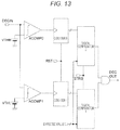
- FIG. 13 shows a configuration of a judge device which operates according to the principles of FIG. 12 .
- the threshold voltages VTHH and VTHL are prepared, and analog comparators ACOMP 0 and ACOMP 1 , which respectively receive them, are prepared.
- the outputs of the two analog comparators are respectively counted by a counter 0 and a counter 1 and are compared with an expected values by a digital comparator 0 and a digital comparator 1 . If the transmission/reception circuit is normal, it is expected that the number of times the loopback addition output input to DECIN crosses VTHH within a certain period and the number of times it crosses VTHL are the same; therefore, the values of the counter 0 and the counter 1 are compared with the same expected value.
- the operation in the internal-signal loopback test of the minute delay circuit is assigned to the reception operation, but can be also assigned to a transmission operation.
- FIG. 15 shows an example in which the operation in the internal-signal loopback test of the minute delay circuit is assigned to the transmission operation.
- a selector 1501 inputs the waveform signal S to the minute delay circuit 7024 in the case of normal transmission and selects and inputs the loopback-test waveform signal TS thereto in the loopback test.
- a selector 1502 inputs the reception signal to the minute delay circuit 7024 in the case of normal reception and passes the minute delay circuit and inputs that to the adder circuit 703 in the case of loopback test.
- the internal-signal loopback test method in which the switch-off state is obtained in the case of transmission, wherein the reception circuit is separated from the high-voltage drive signal generated by the transmission circuit to prevent electric breakdown; and the switch-on state is obtained in the case of reception, wherein the transmission/reception separation switch circuit which causes the minute reception signal from the oscillator to pass therethrough receives the large-amplitude internal loopback signal from the transmission circuit and attenuates and outputs the signal while ensuring the withstand voltage in the transmission/reception separation switch so that the subsequent low-voltage reception circuit is not destroyed can be realized.
- the switch circuit, the ultrasonic-wave probe, the ultrasonic-wave diagnosis apparatus, and the test method described above in a test of a silicon wafer of an IC or a chip after dicing, a realistic test can be realized for each channel of the oscillator at low cost by causing the probes to abut only the signal pads for transmitting/receiving signals to/from the main-body device without causing the probes to abut the many pads connected to the oscillators, and defective chips can be screened. Furthermore, even after mounting on the probe, the transmission/reception circuit can be electrically tested, and failure due to aging deterioration can be diagnosed.
- the present embodiment if the present embodiment is used, the internal-signal loopback test method in which the large-amplitude internal loopback signal from the transmission circuit is received, and the signal is attenuated and output while ensuring the withstand voltage in the transmission/reception separation switch so that the subsequent low-voltage reception circuit is not destroyed can be realized. More specifically, the present embodiment exerts effects as the techniques for screening defects of transmission/reception circuits of IC at low cost, without electrically contacting the many terminals connected to the oscillators.
- test waveforms may be supplied from a test-waveform generating circuit outside the chip, and judge may be also carried out by a judge circuit outside the chip. Meanwhile, part or all of the test-waveform generating circuit or the judge circuit may be built in the chip in advance. Also, a pre-shipment test may be carried out at the point when the chip is connected to the oscillators and assembled as an ultrasonic-wave probe.
- tests may be periodically carried out during usage by a user (s).
- the tests can be carried out as the tests periodically carried out by a serviceman or in a test mode automatically activated when the power source of the apparatus is ON.
- part or all of the test-waveform generating circuit or the judge circuit may be built in the ultrasonic-wave probe or the diagnosis-apparatus main body or may be formed as a test device carried by a serviceman.
- the present invention is not limited to the above described embodiments, but include various modification examples.
- part of the configuration of one of the embodiments may be replaced by the configuration of another one of the embodiments, and the configuration of one of the embodiments may include the configuration of another one of the embodiments.
- part of the configuration of each of the embodiments can be subjected to addition/deletion/replacement with the configuration of the other embodiments.
- source and drain of a transistor are sometimes replaced by each other, for example, when a transistor of different polarities is employed or when the directions of currents are changed in circuit operations. Therefore, in the present description, the terms “source” and “drain” can be used by replacing them by each other.
- Effects are exerted by mounting on an IC in an ultrasonic-wave probe connected to an ultrasonic-wave diagnosis apparatus.
Landscapes
- Health & Medical Sciences (AREA)
- Life Sciences & Earth Sciences (AREA)
- Engineering & Computer Science (AREA)
- Physics & Mathematics (AREA)
- Surgery (AREA)
- Animal Behavior & Ethology (AREA)
- Radiology & Medical Imaging (AREA)
- Nuclear Medicine, Radiotherapy & Molecular Imaging (AREA)
- Biomedical Technology (AREA)
- Heart & Thoracic Surgery (AREA)
- Medical Informatics (AREA)
- Molecular Biology (AREA)
- Biophysics (AREA)
- Pathology (AREA)
- General Health & Medical Sciences (AREA)
- Public Health (AREA)
- Veterinary Medicine (AREA)
- Gynecology & Obstetrics (AREA)
- General Engineering & Computer Science (AREA)
- General Physics & Mathematics (AREA)
- Ultra Sonic Daignosis Equipment (AREA)
- Electromagnetism (AREA)
- Computer Networks & Wireless Communication (AREA)
- Signal Processing (AREA)
Abstract
Description
VCG=Vdd−4·Vf [Mathematical Expression 3]
VCG=Vdd−4·Vgsd [Mathematical Expression 4]
- MN* NMOS
- MP* FMOS
- C* Capacitor
- R* Resistance
- INV* Logic inverter
- Vdd Power source
- SWIN Switch input
- SWOUT Switch output
- D* Diode
- AFE Analog front end
- IC Integrated Circuit Integrated Circuit
- CW Continuous wave continuous wave
Claims (15)
Applications Claiming Priority (3)
| Application Number | Priority Date | Filing Date | Title |
|---|---|---|---|
| JP2015062295 | 2015-03-25 | ||
| JP2015-062295 | 2015-03-25 | ||
| PCT/JP2016/055706 WO2016152375A1 (en) | 2015-03-25 | 2016-02-25 | Ultrasonic probe, ultrasonic diagnostic device, and method for testing ultrasonic probes |
Publications (2)
| Publication Number | Publication Date |
|---|---|
| US20180035974A1 US20180035974A1 (en) | 2018-02-08 |
| US10595822B2 true US10595822B2 (en) | 2020-03-24 |
Family
ID=56978931
Family Applications (1)
| Application Number | Title | Priority Date | Filing Date |
|---|---|---|---|
| US15/553,197 Active 2037-01-12 US10595822B2 (en) | 2015-03-25 | 2016-02-25 | Ultrasonic-wave probe, ultrasonic-wave diagnosis apparatus, and test method of ultrasonic-wave probe |
Country Status (5)
| Country | Link |
|---|---|
| US (1) | US10595822B2 (en) |
| EP (1) | EP3275374B1 (en) |
| JP (1) | JP6396578B2 (en) |
| CN (1) | CN107405131B (en) |
| WO (1) | WO2016152375A1 (en) |
Families Citing this family (8)
| Publication number | Priority date | Publication date | Assignee | Title |
|---|---|---|---|---|
| EP3480621B1 (en) * | 2017-11-01 | 2022-05-11 | Samsung Medison Co., Ltd. | Ultrasound apparatus and control method thereof |
| JP6779247B2 (en) * | 2018-03-23 | 2020-11-04 | 株式会社日立製作所 | Ultrasonic diagnostic equipment |
| CN109549665B (en) * | 2018-11-15 | 2021-06-22 | 青岛海信医疗设备股份有限公司 | Ultrasonic equipment detection system |
| JP7145056B2 (en) | 2018-11-27 | 2022-09-30 | 富士フイルムヘルスケア株式会社 | Ultrasonic probe and ultrasonic diagnostic equipment |
| JP7552311B2 (en) * | 2020-12-01 | 2024-09-18 | セイコーエプソン株式会社 | Driving circuit and liquid ejection device |
| JP7528751B2 (en) * | 2020-12-01 | 2024-08-06 | セイコーエプソン株式会社 | Driving circuit and liquid ejection device |
| JP7423573B2 (en) * | 2021-04-28 | 2024-01-29 | 富士フイルムヘルスケア株式会社 | Ultrasonic probe and ultrasound diagnostic equipment |
| CN114172498A (en) * | 2021-11-11 | 2022-03-11 | 深圳先进技术研究院 | Switching circuit, integrated circuit, and electronic device |
Citations (7)
| Publication number | Priority date | Publication date | Assignee | Title |
|---|---|---|---|---|
| US20120092954A1 (en) * | 2009-03-04 | 2012-04-19 | Hitachi Medical Corporation | Ultrasonic transmitting/receiving circuit and ultrasonic diagnostic apparatus |
| US20120249210A1 (en) | 2011-03-30 | 2012-10-04 | Hitachi, Ltd. | Switch circuit and semiconductor circuit |
| JP2013197929A (en) | 2012-03-21 | 2013-09-30 | Hitachi Ltd | Semiconductor device, and ultrasonic diagnostic apparatus using the same |
| US20140084997A1 (en) | 2012-09-25 | 2014-03-27 | David Simmonds | Transmit/receive switch with series, doubly-floating device and switched bias voltage |
| US20150374335A1 (en) * | 2013-03-07 | 2015-12-31 | Sharp Kabushiki Kaisha | Ultrasound sensor element, ultrasound sensor array assembly, ultrasound transmit sensor element, imaging device, ultrasound transducer, and method of performing an ultrasound scan |
| US20170209124A1 (en) * | 2016-01-21 | 2017-07-27 | Konica Minolta, Inc. | Ultrasound Probe and Ultrasound Diagnostic Apparatus |
| US20170326588A1 (en) * | 2016-05-11 | 2017-11-16 | EchoNous, Inc. | Systems and methods for ultrasound pulse generation using gallium nitride field effect transistors |
Family Cites Families (8)
| Publication number | Priority date | Publication date | Assignee | Title |
|---|---|---|---|---|
| GB9223770D0 (en) * | 1992-11-12 | 1992-12-23 | Raychem Ltd | Communication channel testing arrangement |
| CA2157150C (en) * | 1995-08-29 | 2005-04-05 | Desmond Hirson | Ultrasound image management system |
| JPH0975342A (en) * | 1995-09-11 | 1997-03-25 | Hitachi Medical Corp | Switch circuit and ultrasonic diagnostic device using the same |
| JP4991355B2 (en) * | 2007-03-14 | 2012-08-01 | 株式会社東芝 | Ultrasonic diagnostic apparatus and ultrasonic probe |
| JP2009229737A (en) * | 2008-03-21 | 2009-10-08 | Nec Electronics Corp | Drive circuit for display device, and method of testing the same |
| WO2010143604A1 (en) * | 2009-06-12 | 2010-12-16 | 株式会社 日立メディコ | Ultrasound diagnosis device and ultrasound probe used in same |
| US9178507B2 (en) * | 2012-11-28 | 2015-11-03 | Analog Devices, Inc. | Apparatus and methods for ultrasound transmit switching |
| JP6038735B2 (en) * | 2013-06-21 | 2016-12-07 | 東芝メディカルシステムズ株式会社 | Ultrasonic diagnostic apparatus and ultrasonic probe |
-
2016
- 2016-02-25 US US15/553,197 patent/US10595822B2/en active Active
- 2016-02-25 CN CN201680013991.4A patent/CN107405131B/en active Active
- 2016-02-25 WO PCT/JP2016/055706 patent/WO2016152375A1/en not_active Ceased
- 2016-02-25 JP JP2017507627A patent/JP6396578B2/en active Active
- 2016-02-25 EP EP16768278.0A patent/EP3275374B1/en active Active
Patent Citations (8)
| Publication number | Priority date | Publication date | Assignee | Title |
|---|---|---|---|---|
| US20120092954A1 (en) * | 2009-03-04 | 2012-04-19 | Hitachi Medical Corporation | Ultrasonic transmitting/receiving circuit and ultrasonic diagnostic apparatus |
| US20120249210A1 (en) | 2011-03-30 | 2012-10-04 | Hitachi, Ltd. | Switch circuit and semiconductor circuit |
| JP2012209763A (en) | 2011-03-30 | 2012-10-25 | Hitachi Ltd | Switch circuit and semiconductor circuit |
| JP2013197929A (en) | 2012-03-21 | 2013-09-30 | Hitachi Ltd | Semiconductor device, and ultrasonic diagnostic apparatus using the same |
| US20140084997A1 (en) | 2012-09-25 | 2014-03-27 | David Simmonds | Transmit/receive switch with series, doubly-floating device and switched bias voltage |
| US20150374335A1 (en) * | 2013-03-07 | 2015-12-31 | Sharp Kabushiki Kaisha | Ultrasound sensor element, ultrasound sensor array assembly, ultrasound transmit sensor element, imaging device, ultrasound transducer, and method of performing an ultrasound scan |
| US20170209124A1 (en) * | 2016-01-21 | 2017-07-27 | Konica Minolta, Inc. | Ultrasound Probe and Ultrasound Diagnostic Apparatus |
| US20170326588A1 (en) * | 2016-05-11 | 2017-11-16 | EchoNous, Inc. | Systems and methods for ultrasound pulse generation using gallium nitride field effect transistors |
Non-Patent Citations (2)
| Title |
|---|
| International Search Report (PCT/ISA/210) issued in PCT Application No. PCT/JP2016/055706 dated Mar. 22, 2016 with English translation (4 pages). |
| Japanese-language Written Opinion (PCT/ISA/237) issued in PCT Application No. PCT/JP2016/055706 dated Mar. 22, 2016 (3 pages). |
Also Published As
| Publication number | Publication date |
|---|---|
| JP6396578B2 (en) | 2018-09-26 |
| EP3275374A4 (en) | 2018-12-05 |
| EP3275374A1 (en) | 2018-01-31 |
| CN107405131A (en) | 2017-11-28 |
| JPWO2016152375A1 (en) | 2017-12-07 |
| CN107405131B (en) | 2020-04-07 |
| EP3275374B1 (en) | 2019-11-27 |
| WO2016152375A1 (en) | 2016-09-29 |
| US20180035974A1 (en) | 2018-02-08 |
Similar Documents
| Publication | Publication Date | Title |
|---|---|---|
| US10595822B2 (en) | Ultrasonic-wave probe, ultrasonic-wave diagnosis apparatus, and test method of ultrasonic-wave probe | |
| EP3157170B1 (en) | Switch circuit, ultrasonic contactor using same, and ultrasonic diagnosis apparatus | |
| US7314445B2 (en) | Integrated low-voltage transmit/receive switch for ultrasound imaging system | |
| EP3435872B1 (en) | Symmetric receiver switch for bipolar pulser | |
| JP2004531929A (en) | Circuit and method for controlling a dynamic bidirectional high-voltage analog switch and an ultrasonic test apparatus equipped with such a circuit | |
| Sun et al. | A 180-V pp integrated linear amplifier for ultrasonic imaging applications in a high-voltage CMOS SOI technology | |
| Jang et al. | Dual-mode integrated circuit for imaging and HIFU with 2-D CMUT arrays | |
| EP1640744A1 (en) | Ultrasonic diagnostic apparatus with low voltage switch in the receive channel | |
| US11619729B2 (en) | Ultrasound apparatus and control method thereof | |
| US11660076B2 (en) | Ultrasonic probe, ultrasonic diagnostic apparatus, and ultrasonic transmission/reception switching method | |
| Kajiyama et al. | T/R switch composed of three HV-MOSFETs with 12.1-μW consumption that enables per-channel self-loopback AC tests and− 18.1-dB switching noise suppression for 3-D ultrasound imaging with 3072-ch transceiver | |
| KR20020029148A (en) | Integrated circuit for generating high voltage pulse for use in a medical ultrasound diagnostic system | |
| Carpenter et al. | High-power gallium nitride HIFU transmitter with integrated real-time current and voltage measurement | |
| JP3980733B2 (en) | Ultrasonic diagnostic equipment | |
| JP2011229630A (en) | Diode bridge type transmission/reception separating circuit, and ultrasonic diagnostic equipment equipped with the same | |
| US11369993B2 (en) | Ultrasonic diagnostic apparatus | |
| Onikienko et al. | High Frequency Half-Bridge GaN-Based Pulse Generator | |
| US20100053831A1 (en) | Wideband overvoltage protection circuit | |
| US12085645B2 (en) | Ultrasonic sensor, ultrasonic image generating apparatus, and ultrasonic diagnostic apparatus | |
| US12115020B2 (en) | Two-dimensional array ultrasonic probe and addition circuit | |
| JP7362474B2 (en) | Voltage output device, ultrasonic diagnostic device, and ultrasonic probe device | |
| JP2014145743A (en) | Semiconductor switch circuit, ultrasonic image diagnostic device and semiconductor tester | |
| Choi et al. | Crossed SMPS MOSFET-based protection circuit for high frequency ultrasound transceivers and transducers | |
| Huang et al. | Multiple-Channel High-Voltage Power Drive Circuit for Medical Ultrasound Scanners | |
| Kajiyama | Small-Area, Low-Power Circuits and Systems for Ultrasound Matrix Probes |
Legal Events
| Date | Code | Title | Description |
|---|---|---|---|
| AS | Assignment |
Owner name: HITACHI, LTD., JAPAN Free format text: ASSIGNMENT OF ASSIGNORS INTEREST;ASSIGNORS:KAJIYAMA, SHINYA;IGARASHI, YUTAKA;KATSUBE, YUSAKU;AND OTHERS;SIGNING DATES FROM 20170705 TO 20170713;REEL/FRAME:043387/0978 |
|
| STPP | Information on status: patent application and granting procedure in general |
Free format text: DOCKETED NEW CASE - READY FOR EXAMINATION |
|
| STPP | Information on status: patent application and granting procedure in general |
Free format text: NON FINAL ACTION MAILED |
|
| STPP | Information on status: patent application and granting procedure in general |
Free format text: RESPONSE TO NON-FINAL OFFICE ACTION ENTERED AND FORWARDED TO EXAMINER |
|
| STPP | Information on status: patent application and granting procedure in general |
Free format text: NOTICE OF ALLOWANCE MAILED -- APPLICATION RECEIVED IN OFFICE OF PUBLICATIONS |
|
| STPP | Information on status: patent application and granting procedure in general |
Free format text: PUBLICATIONS -- ISSUE FEE PAYMENT VERIFIED |
|
| STCF | Information on status: patent grant |
Free format text: PATENTED CASE |
|
| AS | Assignment |
Owner name: FUJIFILM HEALTHCARE CORPORATION, JAPAN Free format text: ASSIGNMENT OF ASSIGNORS INTEREST;ASSIGNOR:HITACHI, LTD.;REEL/FRAME:058026/0559 Effective date: 20211013 |
|
| AS | Assignment |
Owner name: FUJIFILM HEALTHCARE CORPORATION, JAPAN Free format text: CORRECTIVE ASSIGNMENT TO CORRECT THE THE PROPERTY AND APPLICATION NUMBERS PREVIOUSLY RECORDED AT REEL: 058026 FRAME: 0559. ASSIGNOR(S) HEREBY CONFIRMS THE ASSIGNMENT;ASSIGNOR:HITACHI LTD.;REEL/FRAME:058917/0853 Effective date: 20211013 |
|
| MAFP | Maintenance fee payment |
Free format text: PAYMENT OF MAINTENANCE FEE, 4TH YEAR, LARGE ENTITY (ORIGINAL EVENT CODE: M1551); ENTITY STATUS OF PATENT OWNER: LARGE ENTITY Year of fee payment: 4 |
|
| AS | Assignment |
Owner name: FUJIFILM CORPORATION, JAPAN Free format text: MERGER;ASSIGNOR:FUJIFILM HEALTHCARE CORPORATION;REEL/FRAME:070608/0001 Effective date: 20240701 |
|
| AS | Assignment |
Owner name: FUJIFILM CORPORATION, JAPAN Free format text: MERGER;ASSIGNOR:FUJIFILM HEALTHCARE CORPORATION;REEL/FRAME:069869/0940 Effective date: 20240701 |