US10588199B2 - Digital addressable lighting interface (DALI) and power device comprising same - Google Patents
Digital addressable lighting interface (DALI) and power device comprising same Download PDFInfo
- Publication number
- US10588199B2 US10588199B2 US16/302,252 US201716302252A US10588199B2 US 10588199 B2 US10588199 B2 US 10588199B2 US 201716302252 A US201716302252 A US 201716302252A US 10588199 B2 US10588199 B2 US 10588199B2
- Authority
- US
- United States
- Prior art keywords
- dali
- electrode
- transistor
- diode
- signal
- Prior art date
- Legal status (The legal status is an assumption and is not a legal conclusion. Google has not performed a legal analysis and makes no representation as to the accuracy of the status listed.)
- Expired - Fee Related
Links
Images


Classifications
-
- H—ELECTRICITY
- H03—ELECTRONIC CIRCUITRY
- H03K—PULSE TECHNIQUE
- H03K17/00—Electronic switching or gating, i.e. not by contact-making and –breaking
- H03K17/04—Modifications for accelerating switching
- H03K17/041—Modifications for accelerating switching without feedback from the output circuit to the control circuit
- H03K17/0412—Modifications for accelerating switching without feedback from the output circuit to the control circuit by measures taken in the control circuit
- H03K17/04123—Modifications for accelerating switching without feedback from the output circuit to the control circuit by measures taken in the control circuit in field-effect transistor switches
-
- H05B37/0254—
-
- H—ELECTRICITY
- H03—ELECTRONIC CIRCUITRY
- H03K—PULSE TECHNIQUE
- H03K17/00—Electronic switching or gating, i.e. not by contact-making and –breaking
- H03K17/06—Modifications for ensuring a fully conducting state
- H03K17/063—Modifications for ensuring a fully conducting state in field-effect transistor switches
-
- H—ELECTRICITY
- H03—ELECTRONIC CIRCUITRY
- H03K—PULSE TECHNIQUE
- H03K17/00—Electronic switching or gating, i.e. not by contact-making and –breaking
- H03K17/51—Electronic switching or gating, i.e. not by contact-making and –breaking characterised by the components used
- H03K17/78—Electronic switching or gating, i.e. not by contact-making and –breaking characterised by the components used using opto-electronic devices, i.e. light-emitting and photoelectric devices electrically- or optically-coupled
- H03K17/785—Electronic switching or gating, i.e. not by contact-making and –breaking characterised by the components used using opto-electronic devices, i.e. light-emitting and photoelectric devices electrically- or optically-coupled controlling field-effect transistor switches
-
- H—ELECTRICITY
- H05—ELECTRIC TECHNIQUES NOT OTHERWISE PROVIDED FOR
- H05B—ELECTRIC HEATING; ELECTRIC LIGHT SOURCES NOT OTHERWISE PROVIDED FOR; CIRCUIT ARRANGEMENTS FOR ELECTRIC LIGHT SOURCES, IN GENERAL
- H05B47/00—Circuit arrangements for operating light sources in general, i.e. where the type of light source is not relevant
- H05B47/10—Controlling the light source
- H05B47/175—Controlling the light source by remote control
- H05B47/18—Controlling the light source by remote control via data-bus transmission
- H05B47/183—Controlling the light source by remote control via data-bus transmission using digital addressable lighting interface [DALI] communication protocols
-
- H—ELECTRICITY
- H03—ELECTRONIC CIRCUITRY
- H03K—PULSE TECHNIQUE
- H03K17/00—Electronic switching or gating, i.e. not by contact-making and –breaking
- H03K17/06—Modifications for ensuring a fully conducting state
- H03K2017/066—Maximizing the OFF-resistance instead of minimizing the ON-resistance
-
- H—ELECTRICITY
- H04—ELECTRIC COMMUNICATION TECHNIQUE
- H04L—TRANSMISSION OF DIGITAL INFORMATION, e.g. TELEGRAPHIC COMMUNICATION
- H04L69/00—Network arrangements, protocols or services independent of the application payload and not provided for in the other groups of this subclass
- H04L69/30—Definitions, standards or architectural aspects of layered protocol stacks
- H04L69/32—Architecture of open systems interconnection [OSI] 7-layer type protocol stacks, e.g. the interfaces between the data link level and the physical level
Definitions
- the present invention relates to a Digital Addressable Lighting Interface (DALI) interface and a power device including the same.
- DALI Digital Addressable Lighting Interface
- a light emitting diode is widely used as a light source due to low power consumption, high luminance, and the like.
- recent light emitting devices have been employed as backlight devices for lighting devices and large liquid crystal displays (LCDs).
- Such light emitting devices are provided in the form of a package that is easy to be mounted on various devices such as lighting devices.
- a lighting system using a Digital Addressable Lighting Interface (DALI) protocol has been proposed as an approach that can integrate and control a plurality of lighting devices as the proportion of use of LEDs for illumination increases in various aspects.
- the DALI protocol uses half-duplex asynchronous communication to receive a state of a lamp, a state of a stabilizer, a dimming level, and the like as query signals, and enables monitoring through a DALI master.
- the lighting system using the DALI protocol includes a power device for transmitting signals between a terminal device and a DALI master.
- the signal is a signal conforming to the DALI standard, which is a lighting control standard.
- the power device includes a DALI interface for generating a DALI signal.
- An aspect of the present invention is directed to provide a DALI interface for generating a signal suitable for the DALI standard even in various voltage and current conditions of a DALI master, and a power device including the same.
- Another aspect of the present invention is directed to provide a DALI interface for generating a signal suitable for the DALI standard even when there is characteristic deviation in components of the DALI interface, and a power device including the same.
- a further another aspect of the present invention is directed to provide a DALI interface capable of adjusting waveform characteristics of a DALI signal.
- a Digital Addressable Lighting Interface (DALI) interface includes: a first limiting circuit unit for outputting a limited current based on a DALI transmission signal and a DALI reception signal; and a gate drive circuit unit for generating, based on the limited current, a drain-source voltage that is used for generating a DALI signal in accordance with a DALI standard.
- DALI Digital Addressable Lighting Interface
- the gate drive circuit unit may include a first transistor for generating the drain-source voltage.
- the gate drive circuit unit may include a parallel capacitor connected to a gate electrode and a drain electrode of the first transistor and adjusting a falling time and a rising time of the DALI signal.
- the gate drive circuit unit may include a second transistor for controlling the first transistor.
- the gate drive circuit unit may include a Zener diode for allowing a constant voltage to be inputted with regard to the limited current.
- the first limiting circuit unit may include a photocoupler for receiving the DALI transmission signal.
- a Digital Addressable Lighting Interface (DALI) interface includes: a first limiting current unit including a first photocoupler, and a first diode having a cathode electrode connected to a collector electrode of the first photocoupler; and a gate drive circuit unit including a Zener diode having a cathode electrode connected to an emitter electrode of the first photocoupler, a second diode having an anode electrode connected to a cathode electrode of the Zener diode, and a first transistor having a gate electrode connected to a cathode electrode of the second diode, a drain electrode connected to an anode electrode of the first diode, and a source electrode connected to a ground electrode.
- a first limiting current unit including a first photocoupler, and a first diode having a cathode electrode connected to a collector electrode of the first photocoupler
- a gate drive circuit unit including a Zener diode having a cathode electrode connected to an emitter electrode of the
- the gate drive circuit unit may include a parallel capacitor having one end connected to the gate electrode of the first transistor and the other end connected to the drain electrode of the first transistor.
- the gate drive circuit unit may include a second transistor having a base electrode connected to the anode electrode of the second diode, an emitter electrode connected to the gate electrode of the first transistor, and a collector electrode connected to the ground electrode.
- the first limiting circuit unit may include a first smoothing capacitor having one end connected to the collector electrode of the first photocoupler and the cathode electrode of the first diode and the other end connected to the ground electrode.
- a power device includes: a microcontroller for outputting a Digital Addressable Lighting Interface (DALI) transmission signal and receiving a DALI reception signal; and a DALI interface including a first limiting circuit unit for outputting a DALI signal in accordance with a DALI standard and outputting a limited current based on the DALI transmission signal and the DALI reception signal, and a gate drive circuit unit for generating, based on the limited current, a drain-source voltage that is used for generating the DALI signal in accordance with the DALI standard.
- DALI Digital Addressable Lighting Interface
- a lighting system includes: a terminal device for outputting a control signal for controlling a lighting device; a power device including a first limiting circuit unit for outputting a DALI signal in accordance with a DALI standard based on the control signal and outputting a limited current based on a DALI transmission signal and a DALI reception signal, and a gate drive circuit unit for generating, based on the limited current, a drain-source voltage that is used for generating a DALI signal in accordance with the DALI standard, and a DALI master for controlling a lighting device based on the DALI signal.
- a DALI interface according to an embodiment of the present invention may generate a signal suitable for the DALI standard even in various voltage and current conditions of a DALI master.
- a DALI interface according to an embodiment of the present invention may generate a signal suitable for the DALI standard even when there is characteristic deviation in components of the DALI interface.
- a DALI interface according to an embodiment of the present invention is capable of adjusting waveform characteristics of a DALI signal.
- FIG. 1 is a block diagram of a lighting system according to an embodiment of the present invention.
- FIG. 2 is a block diagram of a power device according to an embodiment of the present invention.
- FIG. 3 is a circuit diagram of a DALI interface according to an embodiment of the present invention.
- FIG. 4 is a circuit diagram for describing a first limiting circuit unit of the DALI interface according to an embodiment of the present invention.
- FIG. 5 is a circuit diagram for describing a gate drive circuit unit of the DALI interface according to an embodiment of the present invention.
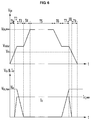
- FIG. 6 is a waveform diagram for describing characteristics of a second transistor of the DALI INTERFACE according to an embodiment of the present invention.
- FIG. 7 is a standard waveform diagram of a DALI signal according to a DALI protocol.
- FIG. 8 is test result according to an embodiment of the present invention.
- FIG. 1 is a block diagram of a lighting system according to an embodiment of the present invention
- FIG. 2 is a block diagram of a power device according to an embodiment of the present invention.
- a lighting system 10 may include a terminal device 100 .
- the terminal device 100 may transmit or receive control information for a plurality of lighting devices to or from a DALI master 300 according to environmental conditions such as time, temperature, or humidity.
- the terminal device 100 may transmit, to the DALI master 300 , control information directly set or inputted by a user. More specifically, the terminal device 100 may provide a DALI transmission (Tx) signal to the power device 200 so as to provide the control information to the DALI master 300 .
- the terminal device 100 may receive a DALI signal generated by the DALI master 300 through the power device 200 in the form of a DALI reception (Rx) signal.
- the terminal device 100 may be a server or a PC.
- the lighting system 10 may include the DALI master 300 .
- the DALI master 300 may provide control information provided from the terminal device 100 to a lighting device (not illustrated) including a DALI communication module.
- the DALI master 300 may transmit control information to a lighting device (not illustrated) directly or using a plurality of DALI slaves (not illustrated). More specifically, the DALI master 300 may receive, from the power device 200 , a DALI signal including control information of a lighting device (not illustrated).
- the DALI master 300 may provide a control signal capable of controlling a lighting device (not illustrated) by using the received DALI signal.
- the DALI master 300 may have various voltage and current conditions according to products.
- the voltage condition of the DALI master 300 may be 9.5 V to 22.5 V.
- the current condition of the DALI master 300 may be 8 mA to 250 mA. Therefore, the DALI master 300 may have various voltage and current conditions.
- the lighting system 10 may include a power device 200 .
- the power device 200 may generate the control signal of the terminal device 100 as a DALI signal suitable for the DALI standard and provide the control signal to the DALI master 300 .
- the power device 200 may include a microcontroller 210 .
- the microcontroller 210 may generate a DALI transmission (Tx) signal according to control information from the terminal device 100 .
- the power device 200 may include a DALI interface 220 .
- the DALI interface 220 may provide the DALI signal to the DALI master 300 by using the DALI transmission (Tx) signal.
- the DALI interface 220 may generate the DALI reception (Rx) signal by using the DALI signal provided from the DALI master 300 , and provide the DALI reception (Rx) signal to the terminal device 100 .
- the DALI interface 220 according to the embodiment of the present invention may generate the DALI signal suitable for the DALI standard even in various voltage and current conditions of the DALI master 300 .
- the DALI interface 220 according to the embodiment of the present invention may generate the DALI signal suitable for the DALI standard even when there is characteristic deviation in components of the DALI interface.
- the DALI interface 220 according to the embodiment of the present invention is capable of adjusting waveform characteristics of the DALI signal.
- FIG. 3 is a circuit diagram of the DALI according to the embodiment of the present invention.
- the DALI interface 220 may include a limiting circuit unit 221 .
- the first limiting circuit unit 221 may provide a limited current to a gate drive circuit unit 222 based on the DALI transmission (Tx) signal or the DALI reception (Rx) signal.
- the first limiting circuit unit 221 may include a first photocoupler PC 1 that receives the DALI transmission (Tx) signal inputted by the microcontroller 210 .
- an anode electrode and a cathode electrode may be connected to the microcontroller 210 .
- the first photocoupler PC 1 may have a collector electrode connected to one end of a first smoothing capacitor C 1 and a cathode electrode of a first diode D 1 .
- the first photocoupler PC 1 may have an emitter electrode connected to a cathode electrode of a Zener diode ZD 1 of the gate drive circuit unit 222 .
- the first limiting circuit unit 221 may include the first smoothing capacitor C 1 .
- the other end of the first smoothing capacitor C 1 may be connected to a first ground electrode GND 1 .
- the first limiting circuit unit 221 may include the first diode D 1 .
- An anode electrode of the first diode D 1 may be connected to one end of a fifth resistor R 5 and a rectification unit 224 .
- the DALI interface 220 may include the gate drive circuit unit 222 .
- the gate drive circuit unit 222 may be controlled by the DALI transmission (Tx) signal.
- the gate drive circuit unit 222 may generate a drain-source voltage V ds by using the limited current of the first limiting circuit unit 221 .
- the drain-source voltage V ds of the gate drive circuit unit 222 may be made to generate the DALI signal suitable for the DALI protocol.
- the gate drive circuit unit 222 may include the Zener diode ZD 1 .
- the Zener diode ZD 1 may constantly maintain a maximum value of an input voltage V ZD1 inputted to the gate drive circuit unit 222 . Therefore, even when a wide range of a supply voltage of the DALI master 300 is provided or a deviation occurs in components of the first photocoupler PC 1 , the Zener diode ZD 1 allows the gate drive circuit unit 222 to operate in a constant input condition.
- the Zener diode ZD 1 may have a cathode electrode connected to a first resistor R 1 , a second resistor R 2 , and the emitter diode of the first photocoupler PC 1 .
- the Zener diode ZD 1 may have an anode electrode connected to the first resistor R 1 , a third resistor R 3 , a fourth resistor R 4 , and a collector electrode of a first transistor Q 1 .
- the gate drive circuit unit 222 may include the first resistor R 1 .
- the first resistor R 1 may be connected in parallel to the Zener diode ZD 1 . That is, the first resistor R 1 may have one end connected to the cathode electrode of the Zener diode ZD 1 and the other end connected to the anode electrode of the Zener diode ZD 1 .
- the gate drive circuit unit 222 may include the second resistor R 2 .
- the second resistor R 2 may have one end connected to the first resistor, the cathode electrode of the Zener diode ZD 1 , and the emitter electrode of the first photocoupler PC 1 .
- the second resistor R 2 may have the other end connected to an anode electrode of a second diode D 2 and a base electrode of the first transistor Q 1 .
- the gate drive circuit unit 222 may include the second diode D 2 .
- the second diode D 2 may have the anode electrode connected to the other end of the second resistor R 2 and the base electrode of the first transistor Q 1 .
- the second diode D 2 may have a cathode electrode connected to the emitter electrode of the first transistor Q 1 , a gate electrode of a second transistor Q 2 , one end of a parallel capacitor C 2 , and one end of the fourth resistor R 4 .
- the gate drive circuit unit 222 may include the first transistor Q 1 .
- the first transistor Q 1 may be a bipolar junction transistor (BJT), but is not limited thereto.
- the first transistor Q 1 may be a PNP type transistor, but is not limited thereto.
- the first transistor Q 1 may have the base electrode connected to the other end of the second resistor R 2 and the anode electrode of the second diode D 2 .
- the first transistor Q 1 may have the emitter electrode connected to the cathode electrode of the second diode D 2 , one end of the parallel capacitor C 2 , one end of the fourth resistor R 4 , and the gate electrode of the second transistor Q 2 .
- the first transistor Q 1 may have the collector electrode connected to one end of the third resistor R 3 .
- the gate drive circuit unit 222 may include the third resistor R 3 .
- the third resistor R 3 may have one end connected to the collector electrode of the first transistor Q 1 and the other end connected to the first ground electrode GND 1 .
- the gate drive circuit unit 222 may include the fourth resistor R 4 .
- the fourth resistor R 4 may have one end connected to the gate electrode of the second transistor Q 2 , one end of the parallel capacitor C 2 , the emitter electrode of the first transistor Q 1 , and the cathode electrode of the second diode D 2 .
- the gate drive circuit unit 222 may include the second transistor Q 2 .
- the second transistor Q 2 may be a metal oxide silicon field effect transistor (MOSFET), but is not limited thereto.
- the second transistor Q 2 may be a PMOS type transistor, but is not limited thereto.
- the second transistor Q 2 may have a gate electrode connected to the cathode electrode of the second diode D 2 , the emitter electrode of the first transistor Q 1 , one end of the fourth resistor R 4 , and one end of the parallel capacitor C 2 .
- the second transistor Q 2 may have a drain electrode connected to the other end of the fifth resistor R 5 .
- the second transistor Q 2 may have a source electrode connected to the first ground electrode GND 1 .
- the gate drive circuit unit 222 may include the parallel capacitor C 2 .
- the parallel capacitor C 2 may be connected in parallel to the gate electrode and the drain electrode of the second transistor Q 2 .
- the parallel capacitor C 2 may have one end connected to the gate electrode of the second transistor Q 2 , one end of the fourth resistor R 4 , the emitter electrode of the first transistor Q 1 , and the cathode electrode of the second diode D 2 .
- the parallel capacitor C 2 may have the other end connected to the drain electrode of the second transistor Q 2 and the other end of the fifth resistor R 5 .
- the DALI interface 220 may include a second limiting circuit unit 223 .
- the second limiting circuit unit 223 may be a current limiting circuit.
- the second limiting circuit unit 223 may limit the current caused by various DALI master conditions so as to be suitable for generating the DALI reception (Rx) signal.
- the DALI interface 220 may include a fifth resistor R 5 .
- the fifth resistor R 5 may provide the drain-source voltage V ds generated by the gate drive circuit unit 222 to the rectification unit 224 .
- the DALI interface 220 may include a second smoothing capacitor C 3 .
- the second smoothing capacitor C 3 may be used to smooth the current inputted from the rectification unit 224 .
- the DALI interface 220 may include the rectification unit 224 .
- the rectification unit 224 may provide the DALI signal to the DALI master 300 based on the drain-source voltage V ds .
- the rectification unit 224 may be implemented by a full bridge diode or a half bridge diode.
- the DALI interface 220 may include the second photocoupler PC 2 which transmits the DALI reception (Rx) signal to the microcontroller 210 .
- FIG. 4 is a circuit diagram for describing the first limiting circuit unit of the DALI interface according to an embodiment of the present invention.
- the DALI interface 220 may receive a DALI transmission (Tx) signal of a high level or a DALI reception (Rx) signal of a high level.
- the first smoothing capacitor C 1 of the first limiting circuit unit 221 may receive a current through the first diode D 1 .
- the first smoothing capacitor C 1 may be charged with a voltage obtained by subtracting a driving voltage V f of the first photocoupler PC 1 from a DALI signal maximum voltage V DALI_max which is a peak value provided from the DALI master. Since the driving voltage V f is 1 V or less, the first photocoupler PC 1 may maintain an off state.
- the DALI interface 220 may receive a DALI transmission (Tx) signal of a high level or a DALI reception (Rx) signal of a low level.
- Tx DALI transmission
- Rx DALI reception
- the first diode D 1 may be turned off.
- the first smoothing capacitor C 1 may maintain a previous state without additional charging or discharging. Since the driving voltage V f is 1 V or less, the first photocoupler PC 1 may maintain an off state.
- the DALI interface 220 may receive a DALI transmission (Tx) signal of a low level or a DALI reception (Rx) signal of a high level.
- Tx DALI transmission
- Rx DALI reception
- the first diode D 1 may be turned off.
- the first smoothing capacitor C 1 may be discharged, and thus a charging voltage may be lowered.
- a driving current I f which is an input current, may flow through the anode electrode of the first photocoupler PC 1 .
- a limited current I C_PC1 may flow through the collector electrode of the first photocoupler PC 1 .
- the limited current I C_PC1 may be limited by I f *CTR (Current Transfer Radio).
- FIG. 5 is a circuit diagram for describing the gate drive circuit unit of the DALI interface according to an embodiment of the present invention
- FIG. 6 is a waveform diagram for describing characteristics of the second transistor of the DALI interface according to an embodiment of the present invention.
- a first period T 1 may be a period in which a gate-source voltage V gs of the second transistor Q 2 increases from 0 V to a threshold voltage V th of the second transistor Q 2 . More specifically, when the DALI transmission (Tx) signal changes from a high level to a low level, the limited current I C_PC1 of the first photocoupler PC 1 may be supplied to the gate electrode of the second transistor Q 2 through the second resistor R 2 and the second diode D 2 . The gate-source voltage V gs of the second transistor Q 2 may increase due to the limited current I C_PC1 .
- the drain-source voltage V ds of the second transistor Q 2 may be a drain maximum voltage D ds_mas according to a maximum supply voltage of the DALI master 300 .
- a drain current Id of the second transistor Q 2 may be 0 V since the second transistor Q 2 is not turned on.
- the first period T 1 may be adjusted by the value of the second resistor R 2 .
- a second period T 2 may be a period in which the gate-source voltage V gs of the second transistor Q 2 increases from the threshold voltage V th to a Miller voltage V miller of the second transistor Q 2 . More specifically, the second transistor Q 2 may reach the threshold voltage V th and be turned on, and a drain-source channel may be formed. The drain current I d of the second transistor Q 2 may increase from 0 V as the gate-source voltage V gs increases.
- the drain current I d of the second transistor Q 2 reaches the drain maximum current I d_max according to the maximum supply current of the DALI master 300 , a Miller effect may be generated by characteristics of the MOSFET, and the gate-source voltage V gs of the second transistor Q 2 may be fixed to the Miller voltage V miller .
- the second period T 2 may be adjusted by the value of the second resistor R 2 .
- a third period T 3 may be a period in which the gate-source voltage V gs of the second transistor Q 2 is maintained at the Miller voltage V miller . More specifically, the drain-source voltage V ds of the second transistor Q 2 may decrease from the drain maximum voltage V ds_max to 0 V. As the drain-source voltage V ds of the second transistor Q 2 decreases, energy charged in the parallel capacitor C 2 may be discharged, and most of the current flowing into the second diode D 2 may flow through the parallel capacitor C 2 . Therefore, the gate-source voltage V gs of the second transistor Q 2 may be maintained at the Miller voltage V miller .
- the third period T 3 may be adjusted by the value of the parallel capacitor C 2 or the second resistor R 2 .
- a falling slope of the drain-source voltage V ds of the second transistor Q 2 may be adjusted by the value of the parallel capacitor C 2 or the second resistor R 2 . Therefore, the DALI interface 220 according to the present invention may adjust a falling time of the DALI signal by adjusting the falling slope of the drain-source voltage V ds of the second transistor Q 2 .
- a fourth period T 4 may be a period in which the gate-source voltage V gs of the second transistor Q 2 increases from the Miller voltage V miller to the gate maximum voltage V gs_max .
- the drain current I d of the second transistor Q 2 may be maintained at the drain maximum current I d_max .
- the drain-source voltage V ds of the second transistor Q 2 may be maintained at the value of [the drain maximum current (I d_max )]*[the driving resistance (R ds_on ) of the second transistor].
- the gate maximum voltage V gs_max may be determined by characteristics of the Zener diode ZD 1 and the value of the second resistor R 2 or the fourth resistor R 4 .
- the fourth period T 4 may be adjusted by the value of the second resistor R 2 .
- a fifth period T 5 may be a period in which the second transistor Q 2 is completely turned on.
- the drain current I d of the second transistor Q 2 may be maintained at the drain maximum current I d_max .
- the drain-source voltage V ds of the second transistor Q 2 may be maintained at the value of [the drain maximum current (I d_max )]*[the driving resistance ( Rds_on ) of the second transistor].
- a sixth period T 6 may be a period in which the gate-source voltage V gs of the second transistor Q 2 decreases from the gate maximum voltage V gs_max to the Miller voltage V miller . More specifically, when the DALI transmission (Tx) signal changes from a low level to a high level, the limited current I C_PC1 of the first photocoupler PC 1 may rapidly decreases, and a voltage V R1 applied across both ends of the first resistor R 1 may decrease. Then, the first transistor Q 1 may be turned on, and the gate-source voltage V gs of the second transistor may decrease.
- the drain current I d and the drain-source voltage V ds of the second transistor Q 2 may maintain a previous state value. That is, the drain current I d of the second transistor Q 2 may be maintained at the drain maximum current I d_max .
- the drain-source voltage V as of the second transistor Q 2 may be maintained at the value of [the drain maximum current (I d_max )]*[the driving resistance (R ds_on ) of the second transistor].
- the sixth period T 6 may be adjusted by the current flowing through the base electrode of the first transistor Q 1 or the value of the third resistor R 3 .
- a seventh period T 7 may be a period in which the gate-source voltage V gs of the second transistor Q 2 is maintained at the Miller voltage V miller . More specifically, the drain-source voltage V ds of the second transistor Q 2 may increase from the value of [the drain maximum current (I d_max )]*[the driving resistance (R ds_on ) of the second transistor] to the drain maximum voltage V ds_max . As the drain-source voltage V ds of the second transistor Q 2 increases, energy is charged in the parallel capacitor C 2 , and at the same time, the current flowing into the parallel capacitor C 2 may flow through the first transistor Q 1 . Therefore, the gate-source voltage V gs of the second transistor Q 2 may be maintained at the Miller voltage V miller .
- the seventh period T 7 may be adjusted by the value of the parallel capacitor C 2 or the third resistor R 3 . That is, a rising slope of the drain-source voltage V ds of the second transistor Q 2 may be adjusted by the value of the parallel capacitor C 2 or the third resistor R 3 . Therefore, the DALI interface 220 according to the present invention may adjust a rising time of the DALI signal by adjusting the rising slope of the drain-source voltage V ds of the second transistor Q 2 .
- An eighth period T 8 may be a period in which the gate-source voltage V gs of the second transistor Q 2 decreases from the Miller voltage V miller to the threshold voltage V th . More specifically, the gate-source voltage V gs of the second transistor Q 2 may reach the threshold voltage V th , the second transistor Q 2 may be turned off, and the drain-source channel may disappear. The drain current I d of the second transistor Q 2 may decrease to 0 V as the gate-source voltage V gs decreases. The eighth period T 8 may be adjusted by the current flowing through the base electrode of the first transistor Q 1 or the value of the third resistor R 3 .
- a ninth period T 9 may be a period in which the gate-source voltage V gs of the second transistor Q 2 decreases from the threshold voltage V th to 0 V. Since the second transistor Q 2 is in the turned-off state, the drain-source voltage V ds and the drain current I d of the second transistor Q 2 may maintain the previous state values. That is, the drain-source voltage V ds of the second transistor Q 2 may be the drain maximum voltage V ds_max , and the drain current I d may be 0 V.
- the ninth period T 9 may be adjusted by the current flowing through the base electrode of the first transistor Q 1 or the value of the third resistor R 3 .
- the DALI interface 220 according to the embodiment of the present invention may generate the DALI signal suitable for the DALI standard by changing the component values of the gate drive circuit unit 222 .
- the DALI interface 220 according to the embodiment of the present invention may generate the DALI signal suitable for the DALI standard by changing the component values of the gate drive circuit unit 222 . That is, the DALI interface 220 according to the embodiment of the present invention is capable of adjusting waveform characteristics such as the rising time, the falling time, and the low-pulse width of the DALI signal so as to be suitable for the DALI standard.
- FIG. 7 is a standard waveform diagram of the DALI signal according to the DALI protocol
- FIG. 8 is a test result according to the embodiment of the present invention.
- the DALI signal should satisfy waveform characteristics according to the standard.
- the DALI signal must have a falling time of 3 ⁇ s to 25 ⁇ s.
- the DALI signal must have a rising time of 3 ⁇ s to 25 ⁇ s.
- the DALI signal must have a low-pulse width of 416 ⁇ s and an error range of about 20%.
- FIG. 8 is a test result when the DALI signals suitable for the DALI standard are generated in different conditions of the DALI master 300 by using the DALI interface 220 according to the present invention.
- the condition of the DALI master 300 is that a DALI voltage V DAU has a maximum value of 17 V, and a DALI current I DAU has a maximum value of 250 mA.
- the DALI interface 220 according to the present invention generated the DALI signal having a falling time of 16.6 ⁇ s, a rising time of 15.2 ⁇ s, and a low-pulse width of 426.6 ⁇ s in the first test condition. Therefore, the DALI interface 220 according to the present invention may generate the DALI signal suitable for the DALI standard in the first test condition.
- the condition of the DALI master 300 is that a DALI voltage V DAU has a maximum value of 15V, and a DALI current I DAU has a maximum value of 8 mA.
- the DALI interface 220 according to the present invention generated the DALI signal having a falling time of 7.2 ⁇ s, a rising time of 19.8 ⁇ s, and a low-pulse width of 447.4 ⁇ s in the second test condition. Therefore, the DALI interface 220 according to the present invention may generate the DALI signal suitable for the DALI standard in the second test condition.
Landscapes
- Electronic Switches (AREA)
- Engineering & Computer Science (AREA)
- Computer Security & Cryptography (AREA)
- Computer Networks & Wireless Communication (AREA)
- Signal Processing (AREA)
- Computing Systems (AREA)
Abstract
Description
Claims (15)
Applications Claiming Priority (3)
| Application Number | Priority Date | Filing Date | Title |
|---|---|---|---|
| KR1020160063052A KR20170132050A (en) | 2016-05-23 | 2016-05-23 | Dali interface and power supply having the same |
| KR10-2016-0063052 | 2016-05-23 | ||
| PCT/KR2017/005028 WO2017204481A1 (en) | 2016-05-23 | 2017-05-16 | Digital addressable lighting interface (dali) and power device comprising same |
Publications (2)
| Publication Number | Publication Date |
|---|---|
| US20190223274A1 US20190223274A1 (en) | 2019-07-18 |
| US10588199B2 true US10588199B2 (en) | 2020-03-10 |
Family
ID=60411813
Family Applications (1)
| Application Number | Title | Priority Date | Filing Date |
|---|---|---|---|
| US16/302,252 Expired - Fee Related US10588199B2 (en) | 2016-05-23 | 2017-05-16 | Digital addressable lighting interface (DALI) and power device comprising same |
Country Status (4)
| Country | Link |
|---|---|
| US (1) | US10588199B2 (en) |
| EP (1) | EP3468154A4 (en) |
| KR (1) | KR20170132050A (en) |
| WO (1) | WO2017204481A1 (en) |
Families Citing this family (4)
| Publication number | Priority date | Publication date | Assignee | Title |
|---|---|---|---|---|
| JP7486517B2 (en) | 2019-03-28 | 2024-05-17 | シグニファイ ホールディング ビー ヴィ | Power delivery configuration across the isolation barrier |
| KR102620169B1 (en) | 2023-02-03 | 2024-01-02 | 주식회사카이저솔루션 | Ballaster with energy-saving led lighting control function using commercial power and digital addresable lighting interface |
| KR102620166B1 (en) | 2023-02-03 | 2024-01-02 | 주식회사카이저솔루션 | Energy-saving led lightingg using commercial power and digital addresable lighting interface |
| WO2025147882A1 (en) * | 2024-01-10 | 2025-07-17 | Tridonic Gmbh & Co Kg | Method and apparatus for processing dali signal |
Citations (10)
| Publication number | Priority date | Publication date | Assignee | Title |
|---|---|---|---|---|
| US4755697A (en) | 1985-07-17 | 1988-07-05 | International Rectifier Corporation | Bidirectional output semiconductor field effect transistor |
| US20030036807A1 (en) | 2001-08-14 | 2003-02-20 | Fosler Ross M. | Multiple master digital addressable lighting interface (DALI) system, method and apparatus |
| WO2003081777A1 (en) | 2002-03-26 | 2003-10-02 | Koninklijke Philips Electronics N.V. | Optoelectronic receiver circuit for digital communication |
| US20100207539A1 (en) | 2009-02-18 | 2010-08-19 | Osram Gesellschaft Mit Beschraenkter Haftung | Circuit for controlling an operating device for a light application, operating device and method for operation of the circuit |
| US20100246082A1 (en) | 2007-04-18 | 2010-09-30 | Lutron Electronics Co., Inc. | Communication Circuit for a Digital Electronic Dimming Ballast |
| WO2013159133A2 (en) | 2012-04-26 | 2013-10-31 | Tridonic Gmbh & Co Kg | Interface having transmitter and receiver branch |
| WO2014060922A2 (en) | 2012-10-17 | 2014-04-24 | Koninklijke Philips N.V. | Digital communication receiver interface circuit for line-pair with duty cycle imbalance compensation |
| US20150076994A1 (en) * | 2012-04-12 | 2015-03-19 | Koninklijke Philips N.V. | Digital communication interface circuit for line-pair with individually adjustable transition edges |
| KR20150145683A (en) | 2014-06-20 | 2015-12-30 | 도시바 라이텍쿠 가부시키가이샤 | Data signal receiving circuit for controling lighting |
| US20160143106A1 (en) * | 2014-11-14 | 2016-05-19 | General Electric Company | Method and system for lighting interface messaging with reduced power consumption |
Family Cites Families (1)
| Publication number | Priority date | Publication date | Assignee | Title |
|---|---|---|---|---|
| DE102013221848B4 (en) * | 2013-10-28 | 2025-01-16 | Tridonic Gmbh & Co Kg | Interface with improved transmission branch, corresponding building technology bus system, ballast with such an interface and luminaire with such a ballast |
-
2016
- 2016-05-23 KR KR1020160063052A patent/KR20170132050A/en not_active Abandoned
-
2017
- 2017-05-16 US US16/302,252 patent/US10588199B2/en not_active Expired - Fee Related
- 2017-05-16 WO PCT/KR2017/005028 patent/WO2017204481A1/en not_active Application Discontinuation
- 2017-05-16 EP EP17803000.3A patent/EP3468154A4/en not_active Withdrawn
Patent Citations (13)
| Publication number | Priority date | Publication date | Assignee | Title |
|---|---|---|---|---|
| US4755697A (en) | 1985-07-17 | 1988-07-05 | International Rectifier Corporation | Bidirectional output semiconductor field effect transistor |
| US20030036807A1 (en) | 2001-08-14 | 2003-02-20 | Fosler Ross M. | Multiple master digital addressable lighting interface (DALI) system, method and apparatus |
| WO2003081777A1 (en) | 2002-03-26 | 2003-10-02 | Koninklijke Philips Electronics N.V. | Optoelectronic receiver circuit for digital communication |
| US20050152440A1 (en) | 2002-03-26 | 2005-07-14 | Koninklijke Philips Electronics N.V | Optoelectronic receiver circuit for digital communication |
| US20100246082A1 (en) | 2007-04-18 | 2010-09-30 | Lutron Electronics Co., Inc. | Communication Circuit for a Digital Electronic Dimming Ballast |
| KR20100094421A (en) | 2009-02-18 | 2010-08-26 | 오스람 게젤샤프트 미트 베쉬랭크터 하프퉁 | Circuit for controlling an operating device for a light application, operating device and method for operation of the circuit |
| US20100207539A1 (en) | 2009-02-18 | 2010-08-19 | Osram Gesellschaft Mit Beschraenkter Haftung | Circuit for controlling an operating device for a light application, operating device and method for operation of the circuit |
| US20150076994A1 (en) * | 2012-04-12 | 2015-03-19 | Koninklijke Philips N.V. | Digital communication interface circuit for line-pair with individually adjustable transition edges |
| WO2013159133A2 (en) | 2012-04-26 | 2013-10-31 | Tridonic Gmbh & Co Kg | Interface having transmitter and receiver branch |
| WO2014060922A2 (en) | 2012-10-17 | 2014-04-24 | Koninklijke Philips N.V. | Digital communication receiver interface circuit for line-pair with duty cycle imbalance compensation |
| US20160174340A1 (en) | 2012-10-17 | 2016-06-16 | Koninklijke Philips N.V. | Digital communication receiver interface circuit for line-pair with duty cycle imbalance compensation |
| KR20150145683A (en) | 2014-06-20 | 2015-12-30 | 도시바 라이텍쿠 가부시키가이샤 | Data signal receiving circuit for controling lighting |
| US20160143106A1 (en) * | 2014-11-14 | 2016-05-19 | General Electric Company | Method and system for lighting interface messaging with reduced power consumption |
Non-Patent Citations (2)
| Title |
|---|
| European Search Report dated Dec. 6, 2019 issued in EP Application No. 17803000.3. |
| International Search issued in Application Report (with English Translation) and Written Opinion dated Aug. 29, 2017 issued in Application No. PCT/KR2017/005028. |
Also Published As
| Publication number | Publication date |
|---|---|
| US20190223274A1 (en) | 2019-07-18 |
| WO2017204481A1 (en) | 2017-11-30 |
| EP3468154A4 (en) | 2020-01-08 |
| KR20170132050A (en) | 2017-12-01 |
| EP3468154A1 (en) | 2019-04-10 |
Similar Documents
| Publication | Publication Date | Title |
|---|---|---|
| US10588199B2 (en) | Digital addressable lighting interface (DALI) and power device comprising same | |
| US11272588B2 (en) | Dimming signal processing circuit having multiple functions | |
| US10140931B2 (en) | Shadow mask assemblies and reusing methods of shadow mask assemblies thereof | |
| US8253342B2 (en) | Light emitting diode illumination system | |
| US9183788B2 (en) | Backlight driving circuit, LCD device, and method for driving the backlight driving circuit | |
| US20130033194A1 (en) | Apparatus and method for controlling led driving circuit and apparatus and method for driving led | |
| EP2326145A1 (en) | LED lamp and LED lamp module | |
| TW201143522A (en) | Control of multi-string LED array | |
| US7684219B2 (en) | Multiplexed DC voltage regulation output circuit having control circuit for stabilizing output voltages | |
| US10038502B1 (en) | Lighting device, luminaire, and signboard | |
| CN103533717A (en) | Electronic equipment based on direct current supply communication and control method thereof | |
| CN202873136U (en) | LED lamp control system | |
| US20130307428A1 (en) | Driver device and driving method for driving a load, in particular an led unit | |
| TW201501570A (en) | Dimmable light emitting diode driving circuit | |
| CN209358812U (en) | A USB-powered light strip controller | |
| US20140139110A1 (en) | Led backlight driving circuit, backlight module, and lcd device | |
| CN103561503B (en) | A kind of LED driving power suitable for AC phase-cut dimming | |
| CN115942537A (en) | Dimming interface control circuit compatible with multiple dimming modes and dimming system | |
| CN103096601B (en) | Light emitting diode (LED) power self-adaptive driver | |
| US20160234918A1 (en) | Interface Having an Improved Transmitting Branch | |
| CN103826347B (en) | Control device and light supply apparatus | |
| CN203734893U (en) | Intelligent LED lamp controller based on Z-wave network and control system of intelligent LED lamp controller | |
| CN215121260U (en) | Ceiling fan lamp control circuit and ceiling fan lamp | |
| CN207410561U (en) | LED light adjusting circuits | |
| CN206341453U (en) | A kind of intelligent light control system |
Legal Events
| Date | Code | Title | Description |
|---|---|---|---|
| AS | Assignment |
Owner name: LG INNOTEK CO., LTD., KOREA, REPUBLIC OF Free format text: ASSIGNMENT OF ASSIGNORS INTEREST;ASSIGNORS:YOON, DONG KEUN;YOON, SEOK;LEE, JUN HO;SIGNING DATES FROM 20181107 TO 20181108;REEL/FRAME:047524/0432 |
|
| FEPP | Fee payment procedure |
Free format text: ENTITY STATUS SET TO UNDISCOUNTED (ORIGINAL EVENT CODE: BIG.); ENTITY STATUS OF PATENT OWNER: LARGE ENTITY |
|
| STPP | Information on status: patent application and granting procedure in general |
Free format text: NON FINAL ACTION MAILED |
|
| STPP | Information on status: patent application and granting procedure in general |
Free format text: NOTICE OF ALLOWANCE MAILED -- APPLICATION RECEIVED IN OFFICE OF PUBLICATIONS |
|
| STPP | Information on status: patent application and granting procedure in general |
Free format text: PUBLICATIONS -- ISSUE FEE PAYMENT VERIFIED |
|
| STCF | Information on status: patent grant |
Free format text: PATENTED CASE |
|
| AS | Assignment |
Owner name: SUZHOU LEKIN SEMICONDUCTOR CO., LTD., CHINA Free format text: ASSIGNMENT OF ASSIGNORS INTEREST;ASSIGNOR:LG INNOTEK CO., LTD.;REEL/FRAME:056366/0335 Effective date: 20210520 |
|
| FEPP | Fee payment procedure |
Free format text: MAINTENANCE FEE REMINDER MAILED (ORIGINAL EVENT CODE: REM.); ENTITY STATUS OF PATENT OWNER: LARGE ENTITY |
|
| LAPS | Lapse for failure to pay maintenance fees |
Free format text: PATENT EXPIRED FOR FAILURE TO PAY MAINTENANCE FEES (ORIGINAL EVENT CODE: EXP.); ENTITY STATUS OF PATENT OWNER: LARGE ENTITY |
|
| STCH | Information on status: patent discontinuation |
Free format text: PATENT EXPIRED DUE TO NONPAYMENT OF MAINTENANCE FEES UNDER 37 CFR 1.362 |
|
| FP | Lapsed due to failure to pay maintenance fee |
Effective date: 20240310 |