US10586948B2 - Organic electro-luminescent display device including moisture detection member - Google Patents
Organic electro-luminescent display device including moisture detection member Download PDFInfo
- Publication number
- US10586948B2 US10586948B2 US15/904,932 US201815904932A US10586948B2 US 10586948 B2 US10586948 B2 US 10586948B2 US 201815904932 A US201815904932 A US 201815904932A US 10586948 B2 US10586948 B2 US 10586948B2
- Authority
- US
- United States
- Prior art keywords
- film
- sealing
- dam
- sealing film
- display area
- Prior art date
- Legal status (The legal status is an assumption and is not a legal conclusion. Google has not performed a legal analysis and makes no representation as to the accuracy of the status listed.)
- Active
Links
- 238000001514 detection method Methods 0.000 title claims abstract description 12
- 238000007789 sealing Methods 0.000 claims abstract description 71
- 239000011368 organic material Substances 0.000 claims abstract description 25
- 229910010272 inorganic material Inorganic materials 0.000 claims abstract description 8
- 239000011147 inorganic material Substances 0.000 claims abstract description 8
- 238000002161 passivation Methods 0.000 claims description 19
- 239000007793 ph indicator Substances 0.000 claims description 9
- 239000002195 soluble material Substances 0.000 claims description 7
- CDBYLPFSWZWCQE-UHFFFAOYSA-L Sodium Carbonate Chemical compound [Na+].[Na+].[O-]C([O-])=O CDBYLPFSWZWCQE-UHFFFAOYSA-L 0.000 claims description 4
- KJFMBFZCATUALV-UHFFFAOYSA-N phenolphthalein Chemical group C1=CC(O)=CC=C1C1(C=2C=CC(O)=CC=2)C2=CC=CC=C2C(=O)O1 KJFMBFZCATUALV-UHFFFAOYSA-N 0.000 claims description 4
- 239000000126 substance Substances 0.000 claims description 3
- 229910000029 sodium carbonate Inorganic materials 0.000 claims description 2
- 239000010408 film Substances 0.000 abstract description 67
- 239000000758 substrate Substances 0.000 abstract description 19
- 239000010409 thin film Substances 0.000 abstract description 15
- 239000010410 layer Substances 0.000 description 41
- 230000015572 biosynthetic process Effects 0.000 description 8
- 239000004065 semiconductor Substances 0.000 description 7
- 239000011810 insulating material Substances 0.000 description 5
- 239000011229 interlayer Substances 0.000 description 5
- 239000000463 material Substances 0.000 description 4
- 229910004304 SiNy Inorganic materials 0.000 description 3
- 230000007547 defect Effects 0.000 description 3
- 230000004048 modification Effects 0.000 description 3
- 238000012986 modification Methods 0.000 description 3
- 238000000059 patterning Methods 0.000 description 3
- 239000011347 resin Substances 0.000 description 3
- 229920005989 resin Polymers 0.000 description 3
- VYPSYNLAJGMNEJ-UHFFFAOYSA-N Silicium dioxide Chemical compound O=[Si]=O VYPSYNLAJGMNEJ-UHFFFAOYSA-N 0.000 description 2
- BOTDANWDWHJENH-UHFFFAOYSA-N Tetraethyl orthosilicate Chemical compound CCO[Si](OCC)(OCC)OCC BOTDANWDWHJENH-UHFFFAOYSA-N 0.000 description 2
- 230000005540 biological transmission Effects 0.000 description 2
- 238000005229 chemical vapour deposition Methods 0.000 description 2
- 239000004020 conductor Substances 0.000 description 2
- 238000012217 deletion Methods 0.000 description 2
- 230000037430 deletion Effects 0.000 description 2
- 238000002845 discoloration Methods 0.000 description 2
- 238000000034 method Methods 0.000 description 2
- 239000011342 resin composition Substances 0.000 description 2
- 229910052814 silicon oxide Inorganic materials 0.000 description 2
- 229910052581 Si3N4 Inorganic materials 0.000 description 1
- 239000002253 acid Substances 0.000 description 1
- 239000000956 alloy Substances 0.000 description 1
- 229910045601 alloy Inorganic materials 0.000 description 1
- 230000000694 effects Effects 0.000 description 1
- 239000011521 glass Substances 0.000 description 1
- 230000005525 hole transport Effects 0.000 description 1
- 230000001771 impaired effect Effects 0.000 description 1
- 239000012535 impurity Substances 0.000 description 1
- AMGQUBHHOARCQH-UHFFFAOYSA-N indium;oxotin Chemical compound [In].[Sn]=O AMGQUBHHOARCQH-UHFFFAOYSA-N 0.000 description 1
- 238000002347 injection Methods 0.000 description 1
- 239000007924 injection Substances 0.000 description 1
- 230000009545 invasion Effects 0.000 description 1
- 150000002500 ions Chemical class 0.000 description 1
- 239000011159 matrix material Substances 0.000 description 1
- 229910052751 metal Inorganic materials 0.000 description 1
- 239000002184 metal Substances 0.000 description 1
- 239000000203 mixture Substances 0.000 description 1
- 229910021420 polycrystalline silicon Inorganic materials 0.000 description 1
- 229920005591 polysilicon Polymers 0.000 description 1
- HQVNEWCFYHHQES-UHFFFAOYSA-N silicon nitride Chemical compound N12[Si]34N5[Si]62N3[Si]51N64 HQVNEWCFYHHQES-UHFFFAOYSA-N 0.000 description 1
- 238000004544 sputter deposition Methods 0.000 description 1
- YVTHLONGBIQYBO-UHFFFAOYSA-N zinc indium(3+) oxygen(2-) Chemical compound [O--].[Zn++].[In+3] YVTHLONGBIQYBO-UHFFFAOYSA-N 0.000 description 1
Images


Classifications
-
- H—ELECTRICITY
- H10—SEMICONDUCTOR DEVICES; ELECTRIC SOLID-STATE DEVICES NOT OTHERWISE PROVIDED FOR
- H10K—ORGANIC ELECTRIC SOLID-STATE DEVICES
- H10K50/00—Organic light-emitting devices
- H10K50/80—Constructional details
- H10K50/84—Passivation; Containers; Encapsulations
- H10K50/844—Encapsulations
-
- H01L51/5253—
-
- G—PHYSICS
- G01—MEASURING; TESTING
- G01N—INVESTIGATING OR ANALYSING MATERIALS BY DETERMINING THEIR CHEMICAL OR PHYSICAL PROPERTIES
- G01N31/00—Investigating or analysing non-biological materials by the use of the chemical methods specified in the subgroup; Apparatus specially adapted for such methods
- G01N31/22—Investigating or analysing non-biological materials by the use of the chemical methods specified in the subgroup; Apparatus specially adapted for such methods using chemical indicators
- G01N31/222—Investigating or analysing non-biological materials by the use of the chemical methods specified in the subgroup; Apparatus specially adapted for such methods using chemical indicators for investigating moisture content
-
- H01L51/0031—
-
- H01L51/5259—
-
- H—ELECTRICITY
- H10—SEMICONDUCTOR DEVICES; ELECTRIC SOLID-STATE DEVICES NOT OTHERWISE PROVIDED FOR
- H10K—ORGANIC ELECTRIC SOLID-STATE DEVICES
- H10K50/00—Organic light-emitting devices
- H10K50/80—Constructional details
- H10K50/84—Passivation; Containers; Encapsulations
- H10K50/846—Passivation; Containers; Encapsulations comprising getter material or desiccants
-
- H—ELECTRICITY
- H10—SEMICONDUCTOR DEVICES; ELECTRIC SOLID-STATE DEVICES NOT OTHERWISE PROVIDED FOR
- H10K—ORGANIC ELECTRIC SOLID-STATE DEVICES
- H10K59/00—Integrated devices, or assemblies of multiple devices, comprising at least one organic light-emitting element covered by group H10K50/00
- H10K59/80—Constructional details
- H10K59/87—Passivation; Containers; Encapsulations
- H10K59/873—Encapsulations
-
- H—ELECTRICITY
- H10—SEMICONDUCTOR DEVICES; ELECTRIC SOLID-STATE DEVICES NOT OTHERWISE PROVIDED FOR
- H10K—ORGANIC ELECTRIC SOLID-STATE DEVICES
- H10K59/00—Integrated devices, or assemblies of multiple devices, comprising at least one organic light-emitting element covered by group H10K50/00
- H10K59/80—Constructional details
- H10K59/87—Passivation; Containers; Encapsulations
- H10K59/874—Passivation; Containers; Encapsulations including getter material or desiccant
-
- H—ELECTRICITY
- H10—SEMICONDUCTOR DEVICES; ELECTRIC SOLID-STATE DEVICES NOT OTHERWISE PROVIDED FOR
- H10K—ORGANIC ELECTRIC SOLID-STATE DEVICES
- H10K71/00—Manufacture or treatment specially adapted for the organic devices covered by this subclass
- H10K71/70—Testing, e.g. accelerated lifetime tests
-
- G—PHYSICS
- G01—MEASURING; TESTING
- G01N—INVESTIGATING OR ANALYSING MATERIALS BY DETERMINING THEIR CHEMICAL OR PHYSICAL PROPERTIES
- G01N31/00—Investigating or analysing non-biological materials by the use of the chemical methods specified in the subgroup; Apparatus specially adapted for such methods
- G01N31/22—Investigating or analysing non-biological materials by the use of the chemical methods specified in the subgroup; Apparatus specially adapted for such methods using chemical indicators
- G01N31/221—Investigating or analysing non-biological materials by the use of the chemical methods specified in the subgroup; Apparatus specially adapted for such methods using chemical indicators for investigating pH value
Definitions
- the present invention relates to organic electro-luminescent (EL) display devices.
- An organic EL display device includes a display panel having a thin film transistor (TFT) and an organic light emitting diode (OLED) formed on a base member.
- TFT thin film transistor
- OLED organic light emitting diode
- a display area including light emitting elements is sealed whereby the light emitting elements are protected against moisture or the like, for example, as is disclosed in Japanese Patent Laid-open Publication No. 2010-272270.
- the sealing is achieved, for example, by a method using a combination of an inorganic material film and an organic material film. If there is a defect in the sealed area, for example, moisture will enter the organic material film and reach the light emitting elements. Such moisture can cause failure in light emission.
- An organic EL display device includes a thin film transistor substrate including a base member; an organic material layer disposed on the base member in a display area and held between a lower electrode and an upper electrode; a dam formed on the base member in an external area surrounding the display area; and a sealing layer formed on the organic material layer, the sealing layer covering the display area, the sealing layer including a sealing planarization film formed of organic material and formed in an area surrounded by the dam, the sealing layer further including a sealing film formed of inorganic material and covering the dam.
- the dam includes moisture detection member.
- FIG. 1 is a schematic plan view of an organic EL display device according to an embodiment of the present invention.
- FIG. 2 is a cross sectional view of the organic EL display device illustrated in FIG. 1 along the line II-II;
- FIG. 3 is a cross sectional view of the organic EL display device illustrated in FIG. 1 along the line III-III.
- FIG. 1 illustrates a schematic structure of an organic electro-luminescent (EL) display device according to an embodiment of the present invention.
- the organic EL display device 1 includes a thin film transistor substrate 10 and a counter substrate 20 opposed to a part of the thin film transistor substrate 10 .
- the thin film transistor substrate 10 has a display area A that displays an image, an external area B surrounding the display area, and a component mount area C.
- the display area A is a substantially rectangular area on which organic light emitting diodes (OLED) (not shown) corresponding to respective pixels are disposed in a matrix.
- the external area B is a frame area surrounding the substantially rectangular display area A. Specific structures of the display area A and the external area B will be described later.
- the component mount area C is a partial area of the thin film transistor substrate 10 , the area having no counter substrate 20 opposed to the area.
- the component mount area C has an external connection terminal 30 .
- the component mount area C may additionally have a driver IC and other components.
- the external connection terminal 30 is a terminal for electrical connection to an external device and is electrically connected to an external device, for example, via a flexible printed circuit board (FPC).
- the external connection terminal 30 receives image data from an external device and supplies a voltage signal to be applied to the respective pixels to the OLEDs via a driver IC (not shown).
- the component mount area C which is defined along one side of the thin film transistor substrate 10 in FIG. 1 , may be defined along two or more sides of the thin film transistor substrate 10 .
- the following describes a specific structure of the display area A and the external area B of the thin film transistor substrate 10 .
- FIG. 2 is a cross sectional view of the organic EL display device 1 illustrated in FIG. 1 along the line II-II. Specifically, FIG. 2 is a schematic cross sectional view of the display area A of the thin film transistor substrate 10 , with the counter substrate 20 omitted.
- the thin film transistor substrate 10 in the display area A has a circuit layer 74 , a planarization film 96 , a passivation film 98 , OLEDs, and a sealing layer 106 sequentially stacked in this order on the base member 70 , the circuit layer 74 including a TFT 72 .
- the base member 70 may be formed, for example, using a glass substrate or a resin film.
- the circuit layer 74 in the display area A includes the TFT 72 and an electric wire (not shown) or the like.
- the circuit layer 74 is formed to drive the OLEDs.
- a part of a driving unit can be formed on the base member 70 as the circuit layer 74 in an area adjacent to the display area A.
- the FPC and the driver IC constituting the driving unit can be connected to the electric wire of the circuit layer 74 in the external area B or the component mount area C.
- abase layer 80 formed of inorganic insulating material is disposed on the base member 70 , and a semiconductor area 82 is formed on the base layer 80 .
- the inorganic insulating material forming the base layer 80 may include, for example, silicon nitride (SiN y ), silicon oxide (SiO x ), and a complex thereof.
- the semiconductor area 82 makes, for example, a channel portion and source and drain portions of a top-gate TFT 72 .
- the semiconductor area 82 is formed of, for example, polysilicon (p-Si).
- the semiconductor area 82 is formed, for example, by forming a semiconductor layer (a p-Si film) on the base member 70 and then patterning the semiconductor layer such that a part thereof for use in the circuit layer 74 is selectively left.
- a gate insulating film 84 On the channel portion of the TFT 72 , a gate insulating film 84 , a gate electrode 86 , and an interlayer insulating layer 88 are formed in this order.
- the interlayer insulating layer 88 covers the gate electrode 86 .
- the gate insulating film 84 is typically formed of Tetraethyl Orthosilicate (TEOS).
- TEOS Tetraethyl Orthosilicate
- the gate electrode 86 is formed by, for example, patterning a metal film formed by sputtering.
- the interlayer insulating layer 88 is formed of, for example, the above mentioned inorganic insulating material. Impurities are doped through ion injection into the semiconductor area 82 constituting the source portion and the drain portion of the TFT 72 .
- a source electrode 90 a and a drain portion 90 b to be electrically connected to the source portion and the drain portion, respectively, of the TFT 72 are formed. With the above, the TFT 72 is formed. After formation of the TFT 72 , as described above, the interlayer insulating film 92 is formed covering the TFT 72 . Further, the planarization film 96 and the passivation film 98 are formed on the interlayer insulating film 92 .
- each OLED includes a lower electrode 100 , an organic material layer 102 , and an upper electrode 104 .
- an OLED is formed by sequentially forming the lower electrode 100 , the organic material layer 102 , and the upper electrode 104 in this order from the base member 70 side.
- the lower electrode 100 corresponds to a positive electrode (anode) of the OLED
- the upper electrode 104 corresponds to a negative electrode (cathode).
- the lower electrode 100 is formed for every pixel in the display area A. Specifically, after formation of the planarization film 96 as described above, a contact hole 110 , through which the lower electrode 100 is to be connected to the TFT 72 , is formed, and a conductive film (not shown), such as an indium tin oxide (ITO) film, is formed inside the contact hole 110 . Then, a passivation film 98 is formed on the planarization film 96 and the conductive film so as to fully cover the base member 70 . Subsequently, the passivation film 98 on the conductive film is removed, and the lower electrode 100 is formed on the conductive film by patterning. With the above, the lower electrode 100 connected to the TFT 72 is formed for every pixel. Note that each lower electrode is formed of light transmission conductive material, such as, ITO or Indium Zinc Oxide (IZO).
- ITO indium tin oxide
- a rib 112 is formed on the boundary between pixels.
- the lower electrode 100 remains uncovered in the effective area of a pixel, the effective area being defined by the surrounding rib 112 .
- an organic material layer 102 is formed on the lower electrode 100 .
- the organic material layer 102 includes a light emitting layer.
- the organic material layer 102 includes a hole transport layer, a light emitting layer, an electron transport layer, or the like.
- the upper electrode 104 is formed covering the entire organic material layer 102 in the display area A.
- the thus formed upper electrode 104 is commonly in contact with the organic material layers 102 of the plurality of OLEDs in the display area A.
- the upper electrode 104 is formed of light transmission conductive material, such as an ultra-thin alloy of Mg and Ag, ITO, or IZO.
- the sealing layer 106 is formed on the upper electrode 104 so as to fully cover the display area A.
- the sealing layer 106 has a laminated structure including a first sealing film 161 , a sealing planarization film 160 , and a second sealing film 162 stacked in this order.
- the first sealing film 161 and the second sealing film 162 are formed of inorganic material (for example, inorganic insulating material).
- the first sealing film 161 and the second sealing film 162 are formed by forming an SiN y film by chemical vapor deposition (CVD).
- the sealing planarization film 160 is formed of organic material (for example, resin material, such as curable resin composition).
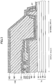
- FIG. 3 is a cross sectional view of the organic EL display device 1 illustrated in FIG. 1 along the line III-III. Specifically, FIG. 3 is a schematic cross sectional view of apart of the thin film transistor substrate 10 between the display area A and the external area B, with the counter substrate 20 and the details of the circuit layer 74 not shown.
- the external area B of the thin film transistor substrate 10 differs from the display area A in that, for example, the former does not include the TFT 72 and the OLEDs.
- the circuit layer 74 , the passivation film 98 , and the sealing layer 106 are formed in this order on the base member 70 .
- a dam 97 is formed on the base member 70 (the circuit layer 74 ) at a position spaced apart from the planarization film 96 , the dam 97 surrounding the display area A. Additionally, the passivation film 98 , the first sealing film 161 , and the second sealing film 162 are formed so as to cover the dam 97 .
- the passivation film 98 is formed of inorganic insulating material, such as SiN y .
- the passivation film 98 is thinner than the sealing films 161 , 162 . For example, the thickness of each of the sealing films 161 , 162 is about a few ⁇ m, while that of the passivation film 98 is about sub- ⁇ m.
- the planarization film 160 remains inside (the display area A side) the surrounding dam 97 .
- the dam 97 prevents the material forming the planarization film 160 from spreading to the outside, for example, when forming the planarization film 160 having a predetermined thickness (for example, about 10 ⁇ m). In the example illustrated, the dam 97 blocks the planarization film 160 from spreading.
- the dam 97 is formed of resin material (for example, photosensitive resin composition) into a linear shape having predetermined width and height. In one embodiment, the dam 97 is formed when forming the planarization film 96 in the display area A.
- the dam 97 includes moisture detection member.
- the dam 97 changes its color in the presence of moisture. Note here that it will take a relatively long time after formation of the passivation film 98 covering the dam 97 until formation of the sealing film 106 (the first sealing film 161 ).
- the external area B remains uncovered while the OLEDs are being formed in the display area A. In other words, the external area B is left in a condition in which foreign bodies are readily deposited on the external area B until formation of the first sealing film 161 .
- the first sealing film 161 on the dam 97 remains uncovered, that is, in a condition in which foreign bodies are readily deposited on the first sealing film 161 , while the planarization film 160 is being formed.
- the passivation film 98 is very thin, and highly likely has a defect. A foreign body, if any, on the dam 97 will highly likely cause a defect because the planarization film 160 is not formed on the dam 97 and the foreign body on the dam 97 is thus not fully covered.
- inclusion of the moisture detection member in the dam 97 to which moisture likely invades, enables early detection of such invasion of moisture.
- the dam 97 (the moisture detection member) contains a pH indicator and water-soluble material that is selected depending on the pH indicator used. Specifically, in the case where a pH indicator (for example, phenolphthalein) having a discoloration region on the alkaline side, for example, a pH indicator being colored on the alkaline side relative to the discoloration region but transparent on the acid side, is used, basic substance (for example, sodium carbonate) is used as water-soluble material.
- the content rate of the pH indicator and the water-soluble material is, for example, 1 wt % to 3 wt % of the material forming the dam 97 .
- the planarization film 96 can have the composition same as that of the dam 97 .
- the planarization film 96 can contain the above mentioned pH indicator and water-soluble material.
- the sealing planarization film 160 may contain moisture detection member.
- the sealing planarization film 160 may be formed of organic material containing the above mentioned pH indicator and water-soluble material.
- the circuit layer 74 in the external area B has, for example, an electric wire (not shown).
- the sealing layer 106 is not formed on the outside of the dam 97 and in the component mount area C, for example, to allow readily connection of various components.
Landscapes
- Life Sciences & Earth Sciences (AREA)
- Health & Medical Sciences (AREA)
- Physics & Mathematics (AREA)
- General Health & Medical Sciences (AREA)
- Immunology (AREA)
- Chemical & Material Sciences (AREA)
- Analytical Chemistry (AREA)
- Biochemistry (AREA)
- Biophysics (AREA)
- General Physics & Mathematics (AREA)
- Molecular Biology (AREA)
- Pathology (AREA)
- Engineering & Computer Science (AREA)
- Manufacturing & Machinery (AREA)
- Optics & Photonics (AREA)
- Electroluminescent Light Sources (AREA)
- Devices For Indicating Variable Information By Combining Individual Elements (AREA)
Abstract
Description
Claims (7)
Applications Claiming Priority (2)
| Application Number | Priority Date | Filing Date | Title |
|---|---|---|---|
| JP2017-037946 | 2017-03-01 | ||
| JP2017037946A JP6830011B2 (en) | 2017-03-01 | 2017-03-01 | Organic EL display device |
Publications (2)
| Publication Number | Publication Date |
|---|---|
| US20180254435A1 US20180254435A1 (en) | 2018-09-06 |
| US10586948B2 true US10586948B2 (en) | 2020-03-10 |
Family
ID=63355329
Family Applications (1)
| Application Number | Title | Priority Date | Filing Date |
|---|---|---|---|
| US15/904,932 Active US10586948B2 (en) | 2017-03-01 | 2018-02-26 | Organic electro-luminescent display device including moisture detection member |
Country Status (2)
| Country | Link |
|---|---|
| US (1) | US10586948B2 (en) |
| JP (1) | JP6830011B2 (en) |
Families Citing this family (5)
| Publication number | Priority date | Publication date | Assignee | Title |
|---|---|---|---|---|
| KR101974086B1 (en) * | 2016-09-30 | 2019-05-02 | 삼성디스플레이 주식회사 | Display module |
| CN109585676B (en) * | 2018-11-28 | 2020-10-27 | 云谷(固安)科技有限公司 | Display panel |
| CN111106267B (en) * | 2019-12-31 | 2021-02-09 | 华中科技大学 | Flexible display electrofluid atomization film packaging system and process |
| CN111668271B (en) * | 2020-06-11 | 2021-08-24 | 武汉华星光电半导体显示技术有限公司 | OLED display panel, preparation method thereof and OLED display device |
| CN111668385B (en) * | 2020-06-15 | 2022-11-04 | Tcl华星光电技术有限公司 | Display panel and packaging method thereof |
Citations (2)
| Publication number | Priority date | Publication date | Assignee | Title |
|---|---|---|---|---|
| US20100295759A1 (en) * | 2009-05-20 | 2010-11-25 | Hitachi Displays, Ltd. | Organic electroluminescence display device |
| US20160372528A1 (en) * | 2013-12-06 | 2016-12-22 | Sharp Kabushiki Kaisha | Light-emitting substrate, photovoltaic cell, display device, lighting device, electronic device, organic light-emitting diode, and method of manufacturing light-emitting substrate |
Family Cites Families (5)
| Publication number | Priority date | Publication date | Assignee | Title |
|---|---|---|---|---|
| US7109653B2 (en) * | 2002-01-15 | 2006-09-19 | Seiko Epson Corporation | Sealing structure with barrier membrane for electronic element, display device, electronic apparatus, and fabrication method for electronic element |
| JP4417027B2 (en) * | 2003-05-21 | 2010-02-17 | 株式会社半導体エネルギー研究所 | Light emitting device |
| JP2016004053A (en) * | 2014-06-13 | 2016-01-12 | 株式会社ジャパンディスプレイ | Display device |
| KR102362189B1 (en) * | 2015-04-16 | 2022-02-11 | 삼성디스플레이 주식회사 | Organic light emitting diode display |
| CN105355645B (en) * | 2015-11-06 | 2019-07-26 | 上海天马微电子有限公司 | A kind of flexible display panels and its manufacturing method, display device |
-
2017
- 2017-03-01 JP JP2017037946A patent/JP6830011B2/en active Active
-
2018
- 2018-02-26 US US15/904,932 patent/US10586948B2/en active Active
Patent Citations (3)
| Publication number | Priority date | Publication date | Assignee | Title |
|---|---|---|---|---|
| US20100295759A1 (en) * | 2009-05-20 | 2010-11-25 | Hitachi Displays, Ltd. | Organic electroluminescence display device |
| JP2010272270A (en) | 2009-05-20 | 2010-12-02 | Hitachi Displays Ltd | Organic el display device |
| US20160372528A1 (en) * | 2013-12-06 | 2016-12-22 | Sharp Kabushiki Kaisha | Light-emitting substrate, photovoltaic cell, display device, lighting device, electronic device, organic light-emitting diode, and method of manufacturing light-emitting substrate |
Also Published As
| Publication number | Publication date |
|---|---|
| JP6830011B2 (en) | 2021-02-17 |
| JP2018147557A (en) | 2018-09-20 |
| US20180254435A1 (en) | 2018-09-06 |
Similar Documents
| Publication | Publication Date | Title |
|---|---|---|
| US10586948B2 (en) | Organic electro-luminescent display device including moisture detection member | |
| US20190013494A1 (en) | Display device | |
| KR102092924B1 (en) | Organic light emitting diode display | |
| US20170117346A1 (en) | Display device | |
| US9704933B2 (en) | Organic electroluminescent device | |
| US10134828B2 (en) | Display device and method of manufacturing a display device | |
| KR20150059478A (en) | Organic electro luminescent device | |
| US10608070B2 (en) | Organic EL display device | |
| US10872948B2 (en) | Electroluminescent display device | |
| CN103681740A (en) | Organic light emitting diode device and method for fabricating the same | |
| US20180083088A1 (en) | Display device | |
| US11349098B2 (en) | Display device with an improved sealing layer | |
| KR20200093718A (en) | Organic light emitting diode display device and method of manufacturing organic light emitting diode display device | |
| CN109979968B (en) | Electroluminescent display device and method of manufacturing the same | |
| US10784459B2 (en) | Display device | |
| US10340327B2 (en) | Display device | |
| JP2015176800A (en) | Light-emitting display device | |
| KR102247825B1 (en) | Bottom Emission Type Organic Light Emission Diode Display Having Color Filters And Method For Manufacturing The Same | |
| US10923536B2 (en) | Organic el display device and method of manufacturing organic el display device | |
| WO2019138495A1 (en) | Display device | |
| US11222940B2 (en) | Display device including a heat dissipation layer in a curved region | |
| US10340478B2 (en) | Organic EL display device and method of manufacturing an organic EL display device |
Legal Events
| Date | Code | Title | Description |
|---|---|---|---|
| AS | Assignment |
Owner name: JAPAN DISPLAY INC., JAPAN Free format text: ASSIGNMENT OF ASSIGNORS INTEREST;ASSIGNOR:SASAKI, YUSUKE;REEL/FRAME:045441/0308 Effective date: 20180124 |
|
| FEPP | Fee payment procedure |
Free format text: ENTITY STATUS SET TO UNDISCOUNTED (ORIGINAL EVENT CODE: BIG.); ENTITY STATUS OF PATENT OWNER: LARGE ENTITY |
|
| STPP | Information on status: patent application and granting procedure in general |
Free format text: FINAL REJECTION MAILED |
|
| STPP | Information on status: patent application and granting procedure in general |
Free format text: DOCKETED NEW CASE - READY FOR EXAMINATION |
|
| STPP | Information on status: patent application and granting procedure in general |
Free format text: EX PARTE QUAYLE ACTION MAILED |
|
| STPP | Information on status: patent application and granting procedure in general |
Free format text: RESPONSE TO EX PARTE QUAYLE ACTION ENTERED AND FORWARDED TO EXAMINER |
|
| STPP | Information on status: patent application and granting procedure in general |
Free format text: NOTICE OF ALLOWANCE MAILED -- APPLICATION RECEIVED IN OFFICE OF PUBLICATIONS |
|
| STPP | Information on status: patent application and granting procedure in general |
Free format text: PUBLICATIONS -- ISSUE FEE PAYMENT RECEIVED |
|
| STCF | Information on status: patent grant |
Free format text: PATENTED CASE |
|
| MAFP | Maintenance fee payment |
Free format text: PAYMENT OF MAINTENANCE FEE, 4TH YEAR, LARGE ENTITY (ORIGINAL EVENT CODE: M1551); ENTITY STATUS OF PATENT OWNER: LARGE ENTITY Year of fee payment: 4 |