US10580779B2 - Vertical transistor static random access memory cell - Google Patents
Vertical transistor static random access memory cell Download PDFInfo
- Publication number
- US10580779B2 US10580779B2 US15/903,203 US201815903203A US10580779B2 US 10580779 B2 US10580779 B2 US 10580779B2 US 201815903203 A US201815903203 A US 201815903203A US 10580779 B2 US10580779 B2 US 10580779B2
- Authority
- US
- United States
- Prior art keywords
- pull
- gate
- transistor
- source
- transistors
- Prior art date
- Legal status (The legal status is an assumption and is not a legal conclusion. Google has not performed a legal analysis and makes no representation as to the accuracy of the status listed.)
- Active, expires
Links
Images


Classifications
-
- H01L27/1104—
-
- H—ELECTRICITY
- H10—SEMICONDUCTOR DEVICES; ELECTRIC SOLID-STATE DEVICES NOT OTHERWISE PROVIDED FOR
- H10D—INORGANIC ELECTRIC SEMICONDUCTOR DEVICES
- H10D30/00—Field-effect transistors [FET]
- H10D30/01—Manufacture or treatment
- H10D30/021—Manufacture or treatment of FETs having insulated gates [IGFET]
- H10D30/025—Manufacture or treatment of FETs having insulated gates [IGFET] of vertical IGFETs
-
- G—PHYSICS
- G11—INFORMATION STORAGE
- G11C—STATIC STORES
- G11C8/00—Arrangements for selecting an address in a digital store
- G11C8/14—Word line organisation; Word line lay-out
-
- H01L21/486—
-
- H01L21/76838—
-
- H01L23/50—
-
- H01L23/5226—
-
- H01L27/1052—
-
- H—ELECTRICITY
- H10—SEMICONDUCTOR DEVICES; ELECTRIC SOLID-STATE DEVICES NOT OTHERWISE PROVIDED FOR
- H10B—ELECTRONIC MEMORY DEVICES
- H10B10/00—Static random access memory [SRAM] devices
- H10B10/12—Static random access memory [SRAM] devices comprising a MOSFET load element
-
- H—ELECTRICITY
- H10—SEMICONDUCTOR DEVICES; ELECTRIC SOLID-STATE DEVICES NOT OTHERWISE PROVIDED FOR
- H10W—GENERIC PACKAGES, INTERCONNECTIONS, CONNECTORS OR OTHER CONSTRUCTIONAL DETAILS OF DEVICES COVERED BY CLASS H10
- H10W20/00—Interconnections in chips, wafers or substrates
- H10W20/01—Manufacture or treatment
- H10W20/031—Manufacture or treatment of conductive parts of the interconnections
-
- H—ELECTRICITY
- H10—SEMICONDUCTOR DEVICES; ELECTRIC SOLID-STATE DEVICES NOT OTHERWISE PROVIDED FOR
- H10W—GENERIC PACKAGES, INTERCONNECTIONS, CONNECTORS OR OTHER CONSTRUCTIONAL DETAILS OF DEVICES COVERED BY CLASS H10
- H10W20/00—Interconnections in chips, wafers or substrates
- H10W20/40—Interconnections external to wafers or substrates, e.g. back-end-of-line [BEOL] metallisations or vias connecting to gate electrodes
- H10W20/41—Interconnections external to wafers or substrates, e.g. back-end-of-line [BEOL] metallisations or vias connecting to gate electrodes characterised by their conductive parts
- H10W20/42—Vias, e.g. via plugs
-
- H—ELECTRICITY
- H10—SEMICONDUCTOR DEVICES; ELECTRIC SOLID-STATE DEVICES NOT OTHERWISE PROVIDED FOR
- H10W—GENERIC PACKAGES, INTERCONNECTIONS, CONNECTORS OR OTHER CONSTRUCTIONAL DETAILS OF DEVICES COVERED BY CLASS H10
- H10W70/00—Package substrates; Interposers; Redistribution layers [RDL]
- H10W70/01—Manufacture or treatment
- H10W70/05—Manufacture or treatment of insulating or insulated package substrates, or of interposers, or of redistribution layers
- H10W70/095—Manufacture or treatment of insulating or insulated package substrates, or of interposers, or of redistribution layers of vias therein
-
- H—ELECTRICITY
- H10—SEMICONDUCTOR DEVICES; ELECTRIC SOLID-STATE DEVICES NOT OTHERWISE PROVIDED FOR
- H10W—GENERIC PACKAGES, INTERCONNECTIONS, CONNECTORS OR OTHER CONSTRUCTIONAL DETAILS OF DEVICES COVERED BY CLASS H10
- H10W72/00—Interconnections or connectors in packages
-
- H—ELECTRICITY
- H10—SEMICONDUCTOR DEVICES; ELECTRIC SOLID-STATE DEVICES NOT OTHERWISE PROVIDED FOR
- H10D—INORGANIC ELECTRIC SEMICONDUCTOR DEVICES
- H10D89/00—Aspects of integrated devices not covered by groups H10D84/00 - H10D88/00
- H10D89/10—Integrated device layouts
Definitions
- the present disclosure generally relates to the fabrication of semiconductor devices, and, more particularly, to a vertical static random access memory cell and various methods of forming same.
- SRAMs Static Random Access Memory
- DRAMs Dynamic Random Access Memory
- ROMs Read Only Memory
- SRAMs Static Random Access Memory
- DRAMs Dynamic Random Access Memory
- ROMs Read Only Memory
- SRAMs are typically employed in applications where higher speed and/or reduced power consumption is important, e.g., cache memory of a microprocessor, mobile phones and other mobile consumer products, etc. Millions of such memory devices are typically included in even very basic electronic consumer products.
- the reduced operating voltages used in many modern-day conventional integrated circuits are made possible by improvements in design, such as reduced gate insulation thicknesses in the component transistors and improved tolerance controls in lithographic processing.
- reduced design rules make reduced operating voltages essential to limit the effects of hot carriers generated in small size devices operating at higher, previously conventional operating voltages.
- a typical 6T (six transistor) SRAM memory cell 100 includes two NMOS pass gate transistors PG 1 , PG 2 , two PMOS pull-up transistors PU 1 , PU 2 , and two NMOS pull-down transistors PD 1 , PD 2 .
- Each of the PMOS pull-up transistors PU 1 , PU 2 has its gate ( 104 A, 104 B, respectively) connected to the gate ( 106 A, 106 B, respectively) of a corresponding NMOS pull-down transistor PD 1 , PD 2 .
- the PMOS pull-up transistors PU 1 , PU 2 have their drain regions connected to the drain regions of corresponding NMOS pull-down transistors PD 1 , PD 2 to form inverters having a conventional configuration.
- the source regions of the PMOS pull-up transistors PU 1 , PU 2 are connected to a high reference potential, typically VDD, and the source regions of the NMOS pull-down transistors PD 1 , PD 2 are connected to a lower reference potential, typically VSS or ground.
- the gates of the PMOS pull-up transistor PU 1 and the NMOS pull-down transistor PD 1 which make up one inverter, are connected to the drain regions of the transistors PU 2 , PD 2 of the other inverter.
- the gates of the PMOS pull-up transistor PU 2 and the NMOS pull-down transistor PD 2 which make up the other inverter, are connected to the drain regions of the transistors PU 1 , PD 1 .
- the potential present on the drain regions of the transistors PU 1 , PD 1 (node N 1 ) of the first inverter is applied to the gates of the transistors PU 2 , PD 2 of the second inverter and the charge serves to keep the second inverter in an ON or OFF state.
- the logically opposite potential is present on the drain regions of the transistors PU 2 , PD 2 (node N 2 ) of the second inverter and on the gates of the transistors PU 1 , PD 1 of the first inverter, keeping the first inverter in the complementary OFF or ON state relative to the second inverter.
- the latch of the illustrated SRAM cell 100 has two stable states: a first state with a predefined potential present on charge storage node N 1 and a low potential on charge storage node N 2 ; and a second state with a low potential on charge storage node N 1 and the predefined potential on charge storage node N 2 .
- Binary data are recorded by toggling between the two states of the latch.
- Sufficient charge must be stored on the charge storage node, and thus on the coupled gates of the associated inverter, to unambiguously hold one of the inverters “ON” and unambiguously hold the other of the inverters “OFF”, thereby preserving the memory state.
- the stability of an SRAM cell 100 can be quantified by the margin by which the potential on the charge storage nodes can vary from its nominal value while still keeping the SRAM 100 cell in its original state.
- Data is read out of the conventional SRAM cell 100 in a non-destructive manner by selectively coupling each charge storage node (N 1 , N 2 ) to a corresponding one of a pair of complementary bit lines (BLB, BL).
- the selective coupling is accomplished by the aforementioned pass gate transistors PG 1 , PG 2 , where each pass gate transistor is connected between one of the charge storage nodes (N 1 , N 2 ) and one of the complementary bit lines (BLN, BL).
- Word line signals are provided to the gates of the pass gate transistors PG 1 , PG 2 to switch the pass gate transistors ON during data read operations. Charge flows through the ON pass gate transistors to or from the charge storage nodes (N 1 , N 2 ), discharging one of the bit lines and charging the other of the bit lines.
- the voltage changes on the bit lines are sensed by a differential amplifier (not shown).
- the bit lines BLB, BL are typically equalized at a voltage midway between the high and low reference voltages, typically 1 ⁇ 2 (VDD-VSS), and then a signal on the word line WL turns the pass gate transistors PG 1 , PG 2 ON.
- VDD-VSS voltage midway between the high and low reference voltages
- a signal on the word line WL turns the pass gate transistors PG 1 , PG 2 ON.
- N 1 is charged to a predetermined potential of VDD and N 2 is charged to a lower potential VSS.
- the pass gate transistors PG 1 , PG 2 turn ON, charge begins flowing from node N 1 through pass gate transistor PG 1 to bit line BL.
- the charge on node N 1 begins to drain off to the bit line BLB and is replenished by charge flowing through pull-up transistor PU 1 to node N 1 .
- charge begins to accumulate on charge storage node N 2 which, on charging to a certain level, can begin turning OFF pull-up transistor PU 1 .
- At least one of the charge storage nodes (N 1 , N 2 ) within the SRAM cell 100 must charge or discharge at a faster rate than charge flows from or to the corresponding bit line.
- one technique used to achieve this control is to configure the various transistors of the SRAM cell 100 such that the pass gate transistors PG 1 , PG 2 are strong enough to over-write the pull-up transistors PU 1 , PU 2 during a write operation, but weak enough so as to not over-write the pull-down transistors PD 1 , PD 2 during a read operation.
- the present disclosure is directed to various methods and resulting devices that may avoid, or at least reduce, the effects of one or more of the problems identified above.
- An illustrative memory cell disclosed herein includes a plurality of vertical transistors including first and second pass gate transistors, first and second pull-up transistors, and first and second pull-down transistors.
- Each of the plurality of vertical transistors includes a pillar of semiconductor material, a first source/drain region on a lower portion of the pillar, a gate structure disposed around the pillar above the first source/drain region, and a second source/drain region on a top portion of the pillar above the gate electrode.
- a first bottom electrode connects the source/drain regions of first and second pull-up transistors.
- a second bottom electrode connects the source/drain regions of the first and second pull-down transistors.
- a first shared contact connects the top source/drain region of the second pull-up transistor to the gate structure of the first pull-up transistor.
- a second shared contact connects the top source/drain region of the first pull-down transistor to the gate structure of the second pull-down transistor.
- a first top electrode is connected to the top source/drain regions of the first pass gate transistor, the first pull-up transistor, and the second shared contact to define a first storage node of the memory cell.
- a second top electrode is connected to the top source/drain regions of the second pass gate transistor, the second pull-down transistor, and the first shared contact to define a second storage node of the memory cell.
- Another illustrative memory cell disclosed herein includes, among other things, a plurality of vertical transistors including first and second pass gate transistors, first and second pull-up transistors, and first and second pull-down transistors.
- Each of the plurality of vertical transistors includes a pillar of semiconductor material, a first source/drain region on a lower portion of the pillar, a gate structure disposed around the pillar above the first source/drain region, and a second source/drain region on a top portion of the pillar above the gate electrode.
- a first bottom electrode connects the source/drain regions of the first and second pull-up transistors.
- a second bottom electrode connects the source/drain regions of the first and second pull-down transistors.
- a first routing gate connects the gate structures of the first pull-up transistor and the first pull-down transistor.
- a second routing gate connects the gate structures of the second pull-up transistor and the second pull-down transistor.
- a third routing gate is connected to the gate structure of the second pull-up transistor.
- a fourth routing gate is connected to the gate structure of the first pull-up transistor.
- a first shared contact connects the top source/drain region of the second pull-up transistor and the third routing gate.
- a second shared contact connects the top source/drain region of the first pull-down transistor to the fourth routing gate.
- a first top electrode is connected to the top source/drain regions of the first pass gate transistor and the first pull-up transistor, and to the second shared contact to define a first storage node of the memory cell.
- a second top electrode is connected to the top source/drain regions of the second pass gate transistor and the second pull-down transistor, and to the first shared contact to define a second storage node of the memory cell.
- An illustrative method disclosed herein includes, among other things, forming a plurality of vertical transistors including first and second pass gate transistors, first and second pull-up transistors, and first and second pull-down transistors.
- Each of the plurality of vertical transistors includes a pillar of semiconductor material, a first source/drain region on a lower portion of the pillar, a gate structure disposed around the pillar above the first source/drain region, and a second source/drain region on a top portion of the pillar above the gate electrode.
- a first bottom electrode is formed to connect the source/drain regions of the first and second pull-up transistors.
- a second bottom electrode is formed to connect the source/drain regions of the first and second pull-down transistors.
- a dielectric layer is formed between the plurality of vertical transistors.
- a first shared contact is formed embedded in the dielectric layer to connect the top source/drain region of the second pull-up transistor to the gate structure of the first pull-up transistor.
- a second shared contact is formed embedded in the dielectric layer to connect the top source/drain region of the first pull-down transistor to the gate structure of the second pull-down transistor.
- a first top electrode is formed embedded in the dielectric layer to connect to the top source/drain regions of the first pass gate transistor, the first pull-up transistor, and the second shared contact to define a first storage node of the memory cell.
- a second top electrode is formed embedded in the dielectric layer to connect to the top source/drain regions of the second pass gate transistor, the second pull-down transistor, and the first shared contact to define a second storage node of the memory cell.
- FIG. 1 schematically depicts an illustrative prior art SRAM memory device
- FIGS. 2A-2R depict various methods disclosed herein of forming a vertical SRAM cell
- FIG. 3 is a top view of an alternative embodiment of a vertical SRAM cell.
- the present disclosure generally relates to various methods of forming a vertical static random access memory cell and the resulting device. As will be readily apparent to those skilled in the art upon a complete reading of the present application, the present method is applicable to a variety of devices, including, but not limited to, logic devices, memory devices, etc. With reference to the attached figures, various illustrative embodiments of the methods and devices disclosed herein will now be described in more detail.
- FIGS. 2A-2R illustrate various methods for forming a vertical six transistor (6T) static random access memory (SRAM) cell 200 , including pass gate transistors PG 1 , PG 2 , pull-up transistors PU 1 , PU 2 , and pull-down transistors PD 1 , PD 2 .
- the particular arrangement of the transistors may vary.
- FIGS. 2A-2R show a top view and a cross-sectional view of the memory cell 200 in the process of being fabricated.
- FIG. 2A depicts the (SRAM) cell 200 with a hard mask layer 205 (e.g., SiN) formed and patterned above a silicon substrate 210 .
- a hard mask layer 205 e.g., SiN
- the horizontal surface of the substrate 210 is not shown in the top view.
- the hard mask layer 205 may be formed by depositing a layer of hard mask material, forming a photoresist layer above the hard mask material, patterning the photoresist layer and etching the hard mask material in the presence of the photoresist material, as is known to those of ordinary skill in the art.
- FIG. 2B depicts the SRAM cell 200 after an etch process, such as an anisotropic etch process, was performed to remove material from the silicon substrate 210 to define silicon pillars 215 .
- an etch process such as an anisotropic etch process
- FIG. 2B depicts the SRAM cell 200 after an etch process, such as an anisotropic etch process, was performed to remove material from the silicon substrate 210 to define silicon pillars 215 .
- an etch process such as an anisotropic etch process
- FIG. 2C depicts the SRAM cell 200 after sacrificial spacers 220 (e.g., a gate insulation layer (e.g., silicon dioxide) covered by a gate electrode layer (e.g., amorphous silicon)—not separately shown) were formed on sidewalls of the hard mask layers 205 and the pillars 215 .
- the sacrificial spacers 220 serve as dummy gate electrodes that will be later replaced with other materials. In some embodiments, multiple layers may not be used.
- FIG. 2D depicts the SRAM cell 200 after a plurality of implantation processes 225 was performed to form P-type source/drain regions 230 for the PU 1 /PU 2 transistors, and N-type source/drain regions 235 , 240 for the PG 1 /PG 2 transistors and the PD 1 /PD 2 transistors, respectively.
- Separate implantation steps with different dopant types may be performed in the presence of implantation masks (not shown) to define the P-type source/drain region 235 (e.g., B, BF 2 ) and the N-type source/drain regions 235 , 240 (e.g., As, P).
- the implantations may include enhancement implantations, such as LDD and halo implantations. The implantations may be performed using various tilt angles.
- FIG. 2E depicts the SRAM cell 200 after an etching step was performed to extend the pillars 215 to define bottom electrodes 245 , 250 , 255 A, 255 B and to define isolation trenches 257 .
- the bottom electrode 245 serves as a VDD electrode
- the bottom electrode 250 serves as a VSS electrode
- the bottom electrodes 255 A, 255 B serve to connect the PG transistors to those of neighboring cells.
- FIG. 2F depicts the SRAM cell 200 after several processes were performed to deposit a dielectric layer 260 (e.g., silicon dioxide, low-k dielectric, ultra low-k dielectric, etc.) above the pillars 215 and a planarization process was performed to expose the hard mask layer 205 .
- a dielectric layer 260 e.g., silicon dioxide, low-k dielectric, ultra low-k dielectric, etc.
- FIG. 2G depicts the SRAM cell 200 after one or more etch processes were performed to remove the sacrificial spacers 220 (e.g., etch processes for removing the dummy gate electrode layer and the dummy gate insulation layer) to define gate cavities 265 .
- etch processes for removing the dummy gate electrode layer and the dummy gate insulation layer
- FIG. 2H depicts the SRAM cell 200 after several processes were performed to form gate structures 270 in the gate cavities 265 .
- the gate structures 270 may include a gate insulation layer (e.g., HfO 2 , SiO 2 , a different high-k dielectric, etc.) and a gate electrode material layer (e.g., metal, work function material, etc.).
- a gate insulation layer e.g., HfO 2 , SiO 2 , a different high-k dielectric, etc.
- a gate electrode material layer e.g., metal, work function material, etc.
- barrier layers may also be used (not shown).
- the individual layers of the gate structures 270 are not illustrated.
- FIG. 2I depicts the SRAM cell 200 after several processes were performed.
- One or more etch processes were performed to recess the dielectric layer 260 and the gate structures 270 , thereby exposing an upper portion of the pillars 215 .
- One or more implantation processes 275 were performed to form P-type top source/drain regions 280 for the PU 1 /PU 2 transistors, and N-type top source/drain regions 285 for the PG 1 /PG 2 transistors and the PD 1 /PD 2 transistors, respectively.
- Separate implantation steps with different dopant types may be performed in the presence of implantation masks (not shown) to define the P-type top source/drain regions 280 (e.g., B, BF 2 ) and the N-type top source/drain regions 285 (e.g., As, P).
- the implantations may include enhancement implantations, such as LDD and halo implantations. The implantations may be performed using various tilt angles. An anneal was performed to activate the implanted dopants in the top and bottom SD regions 230 . 235 , 240 , 280 , 285 .
- FIG. 2J depicts the SRAM cell 200 after several processes were performed.
- a deposition process and an etch process were performed to form upper spacers 290 (e.g., silicon nitride).
- Another deposition process was performed to form a dielectric layer 295 (e.g., silicon dioxide, low-k dielectric, ultra low-k dielectric, etc.), and a planarization process was performed to expose the hard mask layer 205 .
- FIG. 2K depicts the SRAM cell 200 after a patterned etch process was performed to define routing gate recesses 300 A, 300 B, 300 C, 300 D, 300 E in the dielectric layers 260 , 295 .
- FIG. 2L depicts the SRAM cell 200 after a plurality of processes were performed to define routing gates 305 A (gates of PG 1 /PG 2 ), 305 B (gate of PU 1 ), 305 C (gates of PU 1 and PD 1 )), 305 D (gates of PU 2 /PD 2 ), 305 E (gate of PD 2 ) in the routing gate recesses 300 A, 300 B, 300 C, 300 D, 300 E.
- a deposition process was performed to deposit a routing gate material (e.g., W, TiN, TaN, WSi 2 , TiSi 2 , Al).
- a planarization process was performed to remove portions of the routing gate material extending above the dielectric layer 295 , and a recess etch process was performed to recess the routing gate material.
- FIG. 2M depicts the SRAM cell 200 after several processes were performed.
- a deposition process and an etch process were performed to form spacers 310 (e.g., silicon nitride).
- Another deposition process was performed to form a dielectric layer 315 (e.g., silicon dioxide, low-k dielectric, ultra low-k dielectric, etc.), and a planarization process was performed to expose the hard mask layer 205 .
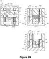
- FIG. 2N depicts the SRAM cell 200 after a patterned anisotropic etch process was performed to form top source/drain contact openings 320 A exposing the top source/drain region 280 of PD 1 and top source/drain contact openings 320 B exposing the top source/drain regions 285 of PG 1 , PG 2 , PD 2 , and to form a shared contact opening 325 A exposing the routing gate 305 B and the top source/drain region 280 of PU 2 and a shared contact opening 325 B exposing the routing gate 305 E and the top source/drain region 285 of PD 1 .
- FIG. 2N includes View B taken through PU 1 and PU 2 .
- FIG. 2O depicts the SRAM cell 200 after the top source/drain contact openings 320 A, 320 B and the shared contact openings 325 A, 325 B are filled with a conductive material (e.g., W, TiN, TiSi, PtSi, Co, Ta) to define top source/drain contacts 330 A, 330 B and shared contacts 335 A. 335 B.
- the shared contact 335 A connects the gate structure 270 of PU 1 to the P-type top source/drain 280 of PU 2 via the routing gate 305 B.
- the shared contact 335 B connects the gate structure 270 of PD 2 to the P-type top source/drain 285 of PD 1 via the routing gate 305 D.
- FIG. 2P depicts the SRAM cell 200 after several processes were performed.
- a dielectric layer 340 (not visible in View A since View A passes through a trench in the dielectric layer 340 ) was formed above the top source/drain contacts 330 A, 330 B and shared contacts 335 A, 335 B.
- a patterned etch process was performed to define trenches in the dielectric layer 340 , and one or more deposition processes were performed to fill the trenches with a conductive material (e.g., W, TiN, TiSi, PtSi, Co, Ta) to define top electrodes 345 A, 345 B.
- the top electrode 345 A contacts the left top source/drain contacts 330 A, 330 B and the shared contact 335 B.
- the top electrode 345 B contacts the right top source/drain contacts 330 A, 330 B and the shared contact 335 A.
- the top electrodes 345 A, 345 B essentially merge with their respective top source/drain contacts 330 A, 330 B and shared contacts 335 A, 335 B.
- the top electrodes 345 A, 345 B define the storage nodes N 1 , N 2 , respectively.
- FIG. 2Q depicts the SRAM cell 200 after several processes were performed.
- FIG. 2Q includes View C taken through PG 1 and PG 2 .
- a dielectric layer 350 was formed above the top electrodes 345 A, 345 B.
- One or more patterned etch processes were performed to define contact openings and trenches in the dielectric layer 350
- one or more deposition processes were performed to fill the contact openings and trenches with a conductive material (e.g., W, TiN, TiSi, PtSi, Co, Ta) to define vias 355 A, 355 B, 355 C, 355 D, 355 E, word line 360 , and word line electrodes 365 A, 365 B, 365 C, 365 D.
- a conductive material e.g., W, TiN, TiSi, PtSi, Co, Ta
- the vias 355 A, 355 B contact the bottom electrodes 255 A, 255 B, respectively.
- the via 355 C contacts the bottom electrode 245 .
- the via 355 D contacts the bottom electrode 250 .
- the via 355 E contacts the routing gate 305 A that connects the gates of PG 1 /PG 2 .
- the word line 360 contacts the via 355 D.
- the word line electrodes 365 A, 365 B contact the vias 355 A, 355 B, respectively.
- the word line electrode 365 C contacts the via 355 C.
- the word line electrode 365 D contacts the via 355 D.
- FIG. 2R depicts the SRAM cell 200 after several processes were performed.
- FIG. 2R includes View D taken through the word line electrode 365 A below PG 1 and PG 2 .
- a dielectric layer 370 was formed above the dielectric layer 350 .
- One or more patterned etch processes were performed to define contact openings and trenches in the dielectric layer 370
- one or more deposition processes were performed to fill the contact openings and trenches with a conductive material (e.g., W, TiN, TiSi, PtSi, Co, Ta) to define vias 375 A, 375 B, 375 C, 375 D, bit lines 380 A (BLB), 380 B (BL), and supply lines 385 A (VSS), 385 B (VDD).
- a conductive material e.g., W, TiN, TiSi, PtSi, Co, Ta
- the via 375 A connects the word line electrode 365 A to the BLB bit line 380 A.
- the via 375 B connects the word line electrode 365 B to the BL bit line 380 B.
- the via 375 C connects the word line electrode 365 C to the VSS supply line 385 A.
- the via 375 D connects the word line electrode 365 D to the VDD supply line 385 B.
- FIG. 3 depicts an SRAM cell 300 with an alternative arrangement of the transistors.
- the locations of the pull up and pull down transistors are reversed.
- the previously described dopant implantation steps for the well regions, LDD and SD implantations would vary according to the new arrangement.
- the VSS and VDD supply lines would also be reversed.
Landscapes
- Engineering & Computer Science (AREA)
- Microelectronics & Electronic Packaging (AREA)
- Semiconductor Memories (AREA)
Abstract
Description
Claims (20)
Priority Applications (1)
| Application Number | Priority Date | Filing Date | Title |
|---|---|---|---|
| US15/903,203 US10580779B2 (en) | 2018-02-23 | 2018-02-23 | Vertical transistor static random access memory cell |
Applications Claiming Priority (1)
| Application Number | Priority Date | Filing Date | Title |
|---|---|---|---|
| US15/903,203 US10580779B2 (en) | 2018-02-23 | 2018-02-23 | Vertical transistor static random access memory cell |
Publications (2)
| Publication Number | Publication Date |
|---|---|
| US20190267387A1 US20190267387A1 (en) | 2019-08-29 |
| US10580779B2 true US10580779B2 (en) | 2020-03-03 |
Family
ID=67684661
Family Applications (1)
| Application Number | Title | Priority Date | Filing Date |
|---|---|---|---|
| US15/903,203 Active 2038-03-22 US10580779B2 (en) | 2018-02-23 | 2018-02-23 | Vertical transistor static random access memory cell |
Country Status (1)
| Country | Link |
|---|---|
| US (1) | US10580779B2 (en) |
Cited By (2)
| Publication number | Priority date | Publication date | Assignee | Title |
|---|---|---|---|---|
| US20220208258A1 (en) * | 2019-09-23 | 2022-06-30 | Institute of Microelectronics Chinese Academy of Sciences | Sram cell, memory comprising the same, and electronic device |
| US20230200039A1 (en) * | 2021-12-21 | 2023-06-22 | Samsung Electronics Co., Ltd. | Integrated circuit and static random access memory (sram) |
Families Citing this family (3)
| Publication number | Priority date | Publication date | Assignee | Title |
|---|---|---|---|---|
| US10741566B2 (en) | 2018-06-26 | 2020-08-11 | Micron Technology, Inc. | Integrated arrangements of pull-up transistors and pull-down transistors, and integrated static memory |
| JP2021048230A (en) * | 2019-09-18 | 2021-03-25 | キオクシア株式会社 | Semiconductor storage device |
| US20240130099A1 (en) * | 2022-10-13 | 2024-04-18 | Taiwan Semiconductor Manufacturing Company, Ltd. | Static random access memory and manufacturing method thereof |
Citations (19)
| Publication number | Priority date | Publication date | Assignee | Title |
|---|---|---|---|---|
| US20040061153A1 (en) | 2002-09-27 | 2004-04-01 | International Business Machines Corporation | Non-volatile memory using ferroelectric gate field-effect transistors |
| US20040113207A1 (en) | 2002-12-11 | 2004-06-17 | International Business Machines Corporation | Vertical MOSFET SRAM cell |
| US20050186760A1 (en) | 2002-06-24 | 2005-08-25 | Toyoda Gosei Co., Ltd. | Semiconductor element and method for producing the same |
| US20060017119A1 (en) | 2004-07-26 | 2006-01-26 | You-Seung Jin | Multi-gate transistor and method of fabricating multi-gate transistor |
| US20070075359A1 (en) | 2005-10-05 | 2007-04-05 | Samsung Electronics Co., Ltd. | Circuit device including vertical transistors connected to buried bitlines and method of manufacturing the same |
| US20080179693A1 (en) | 2007-01-15 | 2008-07-31 | Samsung Electronics Co., Ltd. | Semiconductor device and method of manufacturing a semiconductor device |
| US20080203493A1 (en) | 2007-02-22 | 2008-08-28 | Fujitsu Limited | Semiconductor memory device and fabrication process thereof |
| US20100203714A1 (en) * | 2008-06-20 | 2010-08-12 | Fujio Masuoka | Semiconductor storage device |
| US20100237419A1 (en) | 2009-03-20 | 2010-09-23 | Lie-Yong Yang | Static Random Access Memory (SRAM) Cell and Method for Forming Same |
| US20130109165A1 (en) * | 2011-10-31 | 2013-05-02 | Heung-Jae Cho | Method for manufacturing semiconductor device with vertical gate transistor |
| US20140003133A1 (en) | 2012-06-28 | 2014-01-02 | Synopsys, Inc. | Sram layouts |
| US8754481B2 (en) * | 2011-10-18 | 2014-06-17 | Unisantis Electronics Singapore Pte. Ltd. | Semiconductor device |
| US20150318288A1 (en) * | 2014-05-01 | 2015-11-05 | Globalfoundries Inc. | Vertical transistor static random access memory cell |
| US20160133633A1 (en) | 2014-09-15 | 2016-05-12 | Taiwan Semiconductor Manufacturing Co., Ltd. | Sram cells with vertical gate-all-round mosfets |
| US9472558B1 (en) | 2015-11-13 | 2016-10-18 | Globalfoundries Inc. | Semiconductor structures with stacked non-planar field effect transistors and methods of forming the structures |
| US20170287905A1 (en) | 2013-06-25 | 2017-10-05 | Intel Corporation | MONOLITHIC THREE-DIMENSIONAL (3D) ICs WITH LOCAL INTER-LEVEL INTERCONNECTS |
| US9871103B2 (en) | 2015-07-30 | 2018-01-16 | Samsung Electronics Co., Ltd. | Semiconductor device |
| US20180286957A1 (en) * | 2017-04-03 | 2018-10-04 | Samsung Electronics Co., Ltd. | Semiconductor device |
| US20180294256A1 (en) * | 2017-04-06 | 2018-10-11 | Samsung Electronics Co., Ltd. | Semiconductor devices |
-
2018
- 2018-02-23 US US15/903,203 patent/US10580779B2/en active Active
Patent Citations (19)
| Publication number | Priority date | Publication date | Assignee | Title |
|---|---|---|---|---|
| US20050186760A1 (en) | 2002-06-24 | 2005-08-25 | Toyoda Gosei Co., Ltd. | Semiconductor element and method for producing the same |
| US20040061153A1 (en) | 2002-09-27 | 2004-04-01 | International Business Machines Corporation | Non-volatile memory using ferroelectric gate field-effect transistors |
| US20040113207A1 (en) | 2002-12-11 | 2004-06-17 | International Business Machines Corporation | Vertical MOSFET SRAM cell |
| US20060017119A1 (en) | 2004-07-26 | 2006-01-26 | You-Seung Jin | Multi-gate transistor and method of fabricating multi-gate transistor |
| US20070075359A1 (en) | 2005-10-05 | 2007-04-05 | Samsung Electronics Co., Ltd. | Circuit device including vertical transistors connected to buried bitlines and method of manufacturing the same |
| US20080179693A1 (en) | 2007-01-15 | 2008-07-31 | Samsung Electronics Co., Ltd. | Semiconductor device and method of manufacturing a semiconductor device |
| US20080203493A1 (en) | 2007-02-22 | 2008-08-28 | Fujitsu Limited | Semiconductor memory device and fabrication process thereof |
| US20100203714A1 (en) * | 2008-06-20 | 2010-08-12 | Fujio Masuoka | Semiconductor storage device |
| US20100237419A1 (en) | 2009-03-20 | 2010-09-23 | Lie-Yong Yang | Static Random Access Memory (SRAM) Cell and Method for Forming Same |
| US8754481B2 (en) * | 2011-10-18 | 2014-06-17 | Unisantis Electronics Singapore Pte. Ltd. | Semiconductor device |
| US20130109165A1 (en) * | 2011-10-31 | 2013-05-02 | Heung-Jae Cho | Method for manufacturing semiconductor device with vertical gate transistor |
| US20140003133A1 (en) | 2012-06-28 | 2014-01-02 | Synopsys, Inc. | Sram layouts |
| US20170287905A1 (en) | 2013-06-25 | 2017-10-05 | Intel Corporation | MONOLITHIC THREE-DIMENSIONAL (3D) ICs WITH LOCAL INTER-LEVEL INTERCONNECTS |
| US20150318288A1 (en) * | 2014-05-01 | 2015-11-05 | Globalfoundries Inc. | Vertical transistor static random access memory cell |
| US20160133633A1 (en) | 2014-09-15 | 2016-05-12 | Taiwan Semiconductor Manufacturing Co., Ltd. | Sram cells with vertical gate-all-round mosfets |
| US9871103B2 (en) | 2015-07-30 | 2018-01-16 | Samsung Electronics Co., Ltd. | Semiconductor device |
| US9472558B1 (en) | 2015-11-13 | 2016-10-18 | Globalfoundries Inc. | Semiconductor structures with stacked non-planar field effect transistors and methods of forming the structures |
| US20180286957A1 (en) * | 2017-04-03 | 2018-10-04 | Samsung Electronics Co., Ltd. | Semiconductor device |
| US20180294256A1 (en) * | 2017-04-06 | 2018-10-11 | Samsung Electronics Co., Ltd. | Semiconductor devices |
Non-Patent Citations (7)
| Title |
|---|
| Chung et al., "Novel 4F2 DRAM Cell with Vertical Pillar Transistor (VPT)," 2011 IEEE, pp. 211-214. |
| Huynh-Bal et al., "A Comprehensive Benchmark and Optimization of 5-nm Lateral and Vertical GAA 6T-SRAMs," IEEE Transactions on Electron Devices, 63:643-51, Feb. 2016. |
| Huynh-Bao et al., "Toward the 5nm Technology: Layout Optimization and Performance Benchmark for Logic/SRAMs Using Lateral and Vertical GAA FETs". |
| Notice of Allowance from related U.S. Appl. No. 15/813,471 dated Jul. 5, 2018. |
| Office Action from related U.S. Appl. No. 15/804,556 dated Apr. 16, 2019. |
| Office Action from related U.S. Appl. No. 15/804,556 dated Jul. 18, 2018. |
| Sharma et al., "SRAM Design for Wireless Sensor Networks, Chapter 2 SRAM Bit Cell Optimization," Springer, 2013. |
Cited By (3)
| Publication number | Priority date | Publication date | Assignee | Title |
|---|---|---|---|---|
| US20220208258A1 (en) * | 2019-09-23 | 2022-06-30 | Institute of Microelectronics Chinese Academy of Sciences | Sram cell, memory comprising the same, and electronic device |
| US11482279B2 (en) * | 2019-09-23 | 2022-10-25 | Institute of Microelectronics, Chinese Academy of Sciences | SRAM cell, memory comprising the same, and electronic device |
| US20230200039A1 (en) * | 2021-12-21 | 2023-06-22 | Samsung Electronics Co., Ltd. | Integrated circuit and static random access memory (sram) |
Also Published As
| Publication number | Publication date |
|---|---|
| US20190267387A1 (en) | 2019-08-29 |
Similar Documents
| Publication | Publication Date | Title |
|---|---|---|
| US20150318288A1 (en) | Vertical transistor static random access memory cell | |
| US9831253B2 (en) | FinFET memory device | |
| US7569881B2 (en) | Semiconductor integrated circuit device with reduced leakage current | |
| US10580779B2 (en) | Vertical transistor static random access memory cell | |
| US7307871B2 (en) | SRAM cell design with high resistor CMOS gate structure for soft error rate improvement | |
| US20140027851A1 (en) | Body contacts for fet in soi sram array | |
| US10170377B1 (en) | Memory cell with recessed source/drain contacts to reduce capacitance | |
| CN103378135A (en) | Apparatus for FinFETs | |
| US11424339B2 (en) | Integrated chip and method of forming thereof | |
| US10403629B2 (en) | Six-transistor (6T) SRAM cell structure | |
| TW201701413A (en) | Improved polycrystalline germanium dummy technology to avoid short circuit | |
| US10096606B1 (en) | Methods of forming a gate structure-to-source/drain conductive contact on vertical transistor devices and the resulting transistor devices | |
| US8431455B2 (en) | Method of improving memory cell device by ion implantation | |
| US10418368B1 (en) | Buried local interconnect in source/drain region | |
| US20050224877A1 (en) | Connection structure for SOI devices | |
| US9064733B2 (en) | Contact structure for a semiconductor device and methods of making same | |
| US6576962B2 (en) | CMOS SRAM cell with prescribed power-on data state | |
| WO2002009115A1 (en) | Cmos sram cell with prescribed power-on data state |
Legal Events
| Date | Code | Title | Description |
|---|---|---|---|
| AS | Assignment |
Owner name: GLOBALFOUNDRIES INC., CAYMAN ISLANDS Free format text: ASSIGNMENT OF ASSIGNORS INTEREST;ASSIGNORS:LIM, KWAN-YONG;KIM, RYAN RYOUNG-HAN;SIGNING DATES FROM 20180208 TO 20180223;REEL/FRAME:045015/0517 |
|
| FEPP | Fee payment procedure |
Free format text: ENTITY STATUS SET TO UNDISCOUNTED (ORIGINAL EVENT CODE: BIG.); ENTITY STATUS OF PATENT OWNER: LARGE ENTITY |
|
| STPP | Information on status: patent application and granting procedure in general |
Free format text: FINAL REJECTION MAILED |
|
| STPP | Information on status: patent application and granting procedure in general |
Free format text: ADVISORY ACTION MAILED |
|
| STPP | Information on status: patent application and granting procedure in general |
Free format text: DOCKETED NEW CASE - READY FOR EXAMINATION |
|
| STPP | Information on status: patent application and granting procedure in general |
Free format text: NOTICE OF ALLOWANCE MAILED -- APPLICATION RECEIVED IN OFFICE OF PUBLICATIONS |
|
| STPP | Information on status: patent application and granting procedure in general |
Free format text: PUBLICATIONS -- ISSUE FEE PAYMENT VERIFIED |
|
| STCF | Information on status: patent grant |
Free format text: PATENTED CASE |
|
| AS | Assignment |
Owner name: GLOBALFOUNDRIES U.S. INC., CALIFORNIA Free format text: ASSIGNMENT OF ASSIGNORS INTEREST;ASSIGNOR:GLOBALFOUNDRIES INC.;REEL/FRAME:054633/0001 Effective date: 20201022 |
|
| AS | Assignment |
Owner name: GLOBALFOUNDRIES U.S. INC., NEW YORK Free format text: RELEASE BY SECURED PARTY;ASSIGNOR:WILMINGTON TRUST, NATIONAL ASSOCIATION;REEL/FRAME:056987/0001 Effective date: 20201117 Owner name: GLOBALFOUNDRIES U.S. INC., NEW YORK Free format text: RELEASE OF SECURITY INTEREST;ASSIGNOR:WILMINGTON TRUST, NATIONAL ASSOCIATION;REEL/FRAME:056987/0001 Effective date: 20201117 |
|
| MAFP | Maintenance fee payment |
Free format text: PAYMENT OF MAINTENANCE FEE, 4TH YEAR, LARGE ENTITY (ORIGINAL EVENT CODE: M1551); ENTITY STATUS OF PATENT OWNER: LARGE ENTITY Year of fee payment: 4 |