US10568169B2 - Control circuit, control method and LED driver thereof - Google Patents
Control circuit, control method and LED driver thereof Download PDFInfo
- Publication number
- US10568169B2 US10568169B2 US16/151,453 US201816151453A US10568169B2 US 10568169 B2 US10568169 B2 US 10568169B2 US 201816151453 A US201816151453 A US 201816151453A US 10568169 B2 US10568169 B2 US 10568169B2
- Authority
- US
- United States
- Prior art keywords
- signal
- circuit
- current
- power stage
- generate
- Prior art date
- Legal status (The legal status is an assumption and is not a legal conclusion. Google has not performed a legal analysis and makes no representation as to the accuracy of the status listed.)
- Active
Links
Images


Classifications
-
- H05B33/0815—
-
- H—ELECTRICITY
- H03—ELECTRONIC CIRCUITRY
- H03K—PULSE TECHNIQUE
- H03K5/00—Manipulating of pulses not covered by one of the other main groups of this subclass
- H03K5/22—Circuits having more than one input and one output for comparing pulses or pulse trains with each other according to input signal characteristics, e.g. slope, integral
- H03K5/24—Circuits having more than one input and one output for comparing pulses or pulse trains with each other according to input signal characteristics, e.g. slope, integral the characteristic being amplitude
-
- H—ELECTRICITY
- H05—ELECTRIC TECHNIQUES NOT OTHERWISE PROVIDED FOR
- H05B—ELECTRIC HEATING; ELECTRIC LIGHT SOURCES NOT OTHERWISE PROVIDED FOR; CIRCUIT ARRANGEMENTS FOR ELECTRIC LIGHT SOURCES, IN GENERAL
- H05B45/00—Circuit arrangements for operating light-emitting diodes [LED]
- H05B45/30—Driver circuits
- H05B45/37—Converter circuits
-
- H—ELECTRICITY
- H03—ELECTRONIC CIRCUITRY
- H03L—AUTOMATIC CONTROL, STARTING, SYNCHRONISATION, OR STABILISATION OF GENERATORS OF ELECTRONIC OSCILLATIONS OR PULSES
- H03L7/00—Automatic control of frequency or phase; Synchronisation
- H03L7/06—Automatic control of frequency or phase; Synchronisation using a reference signal applied to a frequency- or phase-locked loop
- H03L7/08—Details of the phase-locked loop
- H03L7/085—Details of the phase-locked loop concerning mainly the frequency- or phase-detection arrangement including the filtering or amplification of its output signal
- H03L7/087—Details of the phase-locked loop concerning mainly the frequency- or phase-detection arrangement including the filtering or amplification of its output signal using at least two phase detectors or a frequency and phase detector in the loop
-
- H05B33/0851—
-
- H—ELECTRICITY
- H05—ELECTRIC TECHNIQUES NOT OTHERWISE PROVIDED FOR
- H05B—ELECTRIC HEATING; ELECTRIC LIGHT SOURCES NOT OTHERWISE PROVIDED FOR; CIRCUIT ARRANGEMENTS FOR ELECTRIC LIGHT SOURCES, IN GENERAL
- H05B45/00—Circuit arrangements for operating light-emitting diodes [LED]
-
- H—ELECTRICITY
- H05—ELECTRIC TECHNIQUES NOT OTHERWISE PROVIDED FOR
- H05B—ELECTRIC HEATING; ELECTRIC LIGHT SOURCES NOT OTHERWISE PROVIDED FOR; CIRCUIT ARRANGEMENTS FOR ELECTRIC LIGHT SOURCES, IN GENERAL
- H05B45/00—Circuit arrangements for operating light-emitting diodes [LED]
- H05B45/30—Driver circuits
- H05B45/305—Frequency-control circuits
-
- H—ELECTRICITY
- H05—ELECTRIC TECHNIQUES NOT OTHERWISE PROVIDED FOR
- H05B—ELECTRIC HEATING; ELECTRIC LIGHT SOURCES NOT OTHERWISE PROVIDED FOR; CIRCUIT ARRANGEMENTS FOR ELECTRIC LIGHT SOURCES, IN GENERAL
- H05B45/00—Circuit arrangements for operating light-emitting diodes [LED]
- H05B45/30—Driver circuits
- H05B45/37—Converter circuits
- H05B45/3725—Switched mode power supply [SMPS]
- H05B45/385—Switched mode power supply [SMPS] using flyback topology
-
- H—ELECTRICITY
- H03—ELECTRONIC CIRCUITRY
- H03L—AUTOMATIC CONTROL, STARTING, SYNCHRONISATION, OR STABILISATION OF GENERATORS OF ELECTRONIC OSCILLATIONS OR PULSES
- H03L7/00—Automatic control of frequency or phase; Synchronisation
- H03L7/06—Automatic control of frequency or phase; Synchronisation using a reference signal applied to a frequency- or phase-locked loop
-
- H—ELECTRICITY
- H05—ELECTRIC TECHNIQUES NOT OTHERWISE PROVIDED FOR
- H05B—ELECTRIC HEATING; ELECTRIC LIGHT SOURCES NOT OTHERWISE PROVIDED FOR; CIRCUIT ARRANGEMENTS FOR ELECTRIC LIGHT SOURCES, IN GENERAL
- H05B45/00—Circuit arrangements for operating light-emitting diodes [LED]
- H05B45/30—Driver circuits
- H05B45/355—Power factor correction [PFC]; Reactive power compensation
-
- H—ELECTRICITY
- H05—ELECTRIC TECHNIQUES NOT OTHERWISE PROVIDED FOR
- H05B—ELECTRIC HEATING; ELECTRIC LIGHT SOURCES NOT OTHERWISE PROVIDED FOR; CIRCUIT ARRANGEMENTS FOR ELECTRIC LIGHT SOURCES, IN GENERAL
- H05B45/00—Circuit arrangements for operating light-emitting diodes [LED]
- H05B45/30—Driver circuits
- H05B45/36—Circuits for reducing or suppressing harmonics, ripples or electromagnetic interferences [EMI]
Definitions
- the present invention generally relates to the field of power electronics, and more particularly to LED drivers, along with associated circuits and methods.
- a switched-mode power supply can include a power stage circuit and a control circuit.
- the control circuit can consider internal parameters and external load changes, and may regulate the on/off times of the switch system in the power stage circuit.
- Switching power supplies have a wide variety of applications in modern electronics. For example, switching power supplies can be used to drive light-emitting diode (LED) loads.
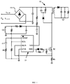
- FIG. 1 is a schematic block diagram of an example LED driver utilizing constant on-time control.
- FIG. 2 is a schematic block diagram of an example LED driver, in accordance with embodiments of the present invention.
- FIG. 3 is a schematic block diagram of another example LED driver, in accordance with embodiments of the present invention.
- FIG. 4 is a schematic block diagram of an example control circuit, in accordance with embodiments of the present invention.
- FIG. 5 is a waveform diagram of example operation of the LED driver, in accordance with embodiments of the present invention.
- FIG. 6 is a waveform diagram of example operation of the LED driver of FIG. 1 .
- FIG. 7 is a schematic block diagram of another example control circuit, in accordance with embodiments of the present invention.
- FIG. 8 is a flow diagram of an example control method, in accordance with an embodiment of the present invention.
- LED lighting is widely used in a wide variety of application fields, such as home, office, outside lighting, and stage lighting.
- An LED driver can drive various types of LED loads in order to provide illumination.
- Designers may expect that the LED driver may have sufficiently high power factor (PF) and sufficiently low total harmonic distortion (THD).
- PF power factor
- TDD total harmonic distortion
- the LED driver can also typically respond quickly to jitters of an alternating current (AC) input power source, in order to eliminate variations of an output current due to the jitters.
- AC alternating current
- the LED driver can include a power stage circuit having rectifier bridge 11 and flyback converter 12 , as well as control circuit 13 .
- Control circuit 13 can obtain a zero-crossing time of an inductor current through auxiliary winding Ln and input the zero-crossing time to terminal ZCS.
- Control circuit 13 can obtain a sample signal of the inductor current through sample resistor Rs and input the sample signal to terminal ISEN.
- a compensation circuit formed by resistor R 1 and capacitor C 1 connected in series can generate a compensation signal at terminal COMP.
- the compensation signal can characterize an error between the inductor current and a desired inductor current, or between the sample signal of the output current and a desired output current.
- Switching control signal Q generated by control circuit 13 can control power transistor M of flyback converter 12 to be turned on or off, such that the output current can be remain substantially constant and tend to be a desired value.
- the resistance of resistor R 1 can be relatively large, and the capacitance of capacitor C 1 can be relatively small, such that the compensation signal can quickly respond to variations of the output current. This can eliminate a sudden change of the output current that may be caused by the instability of the alternating current input power. As a result, control loop circuit with faster response speeds can be formed.
- the control loop circuit can realize quick adjusting, in order to suppress the excess energy caused by input jitter from being transmitted to the output terminal and to keep the output current stable.
- the compensation signal of the control loop circuit may correspond to on-time to ON in each switching cycle.
- control loop circuit can be formed by utilizing a constant on-time control, such that the AC input voltage and input current can be expressed as follows in formulas (1) and (2).
- V IN,AC ( t ) ⁇ square root over (2) ⁇ V AC sin(2 ⁇ f AC t ) (1)
- V IN,AC (t) is the AC input voltage
- ⁇ IN,AC (t) is an average value of the input current in one switching cycle
- V AC is an amplitude of the alternating current input voltage
- f AC is a frequency of the alternating current input power
- L M is the inductance of the inductor of the power stage circuit
- t ON is the on-time
- t S (t) is the switching cycle.
- switching cycle t S (t) can vary within a smaller range in one power frequency cycle, such that the input current can approximately be a sinusoidal signal having the same frequency with the AC input voltage from the entire power frequency cycle.
- the control loop circuit can obtain higher power factor and lower total harmonic distortion by utilizing constant on-time control.
- control loop may have a lower response speed due to constant on-time t ON , and may not solve potential instability problems of the output current that may be caused by jitters of the AC input voltage.
- improved power factor and total harmonic distortion, as well as suppression the influence of jitters of the AC input voltage on the output current can be achieved.
- a control circuit for controlling a power stage circuit of an LED driver can include: (i) a phase-locked loop configured to generate a sinusoidal half-wave signal having the same frequency and phase as an AC input voltage; (ii) a sampling circuit configured to generate a sampling signal of a peak value of an inductor current in the power stage circuit; (iii) a loop compensation circuit configured to generate a loop compensation signal in accordance with the sinusoidal half wave signal and a signal representing an output current of the power stage circuit; and (iv) a switching control signal generating circuit configured to generate a switching control signal for controlling the power stage circuit in accordance with the sampling signal and the loop compensation signal.
- the LED driver can include power stage circuit 1 and control circuit 2 , and power stage circuit 1 can include rectifier circuit 1 A and switching converter 1 B.
- Control circuit 2 can control power stage circuit 1 .
- control circuit 2 can generate a sinusoidal half-wave signal having the same frequency and phase as an AC input voltage by a phase-locked loop, and may generate switching control signal Q to control power stage circuit 1 according to the sinusoidal half-wave signal.
- the phase-locked loop is an automatic closed-loop control circuit to realize phase synchronization of two electrical signals, and can make a phase of an output signal follow a phase of an input signal, thereby keeping the phase consistent.
- the working principle of a phase-locked loop is to detect a phase difference between the input signal and the output signal, and to convert the detected phase difference by a phase detector into a voltage signal.
- the voltage signal generated by the phase detector may be filtered by a low-pass filter to be a control voltage of an oscillator.
- a frequency of the output signal generated by the oscillator can be controlled by the control voltage, and the frequency and phase of the output signal generated by the oscillator can be fed back to the phase detector through a feedback path.
- the phase-locked loop is provided in control circuit 2 , and can generate sinusoidal half-wave signal sin(WAC*t) having a constant amplitude and the same frequency and phase as the AC input voltage.
- Control circuit 2 can generate a switching control signal to control power stage circuit 1 , such that the peak value of the inductor current follows sinusoidal half-wave signal sin(WAC*t). Since sinusoidal half-wave signal sin(WAC*t) has the same frequency and phase as the AC input voltage, the peak value of the inductor current can actually have the same frequency and phase with the AC input voltage. Furthermore, the input current related to the inductor current may follow the AC input voltage, thereby realizing higher power factor and lower total harmonic distortion.
- the amplitude of sinusoidal half-wave signal sin(WAC*t) may not vary following the amplitude of the AC input voltage, such that the peak value of the inductor current can remain stable, effectively preventing sudden changes of the output current that may be caused by the fluctuation of the power grid.
- flyback converter 1 B can perform direct current to direct current conversion on a direct current voltage generated by rectifier bridge 1 A.
- Control circuit 2 can sample the AC input voltage at terminal ACSN by a resistor divider network (e.g., including resistor R 2 and resistor R 3 ) connected to two input terminals of the LED driver, in order to track the frequency and phase of the AC input voltage.
- the AC input voltage can be alternatively sampled directly or indirectly by any other suitable circuit/approach in certain embodiments.
- Resistor R 1 and capacitor C 1 can connect between terminal COMP of the control circuit and ground, in order to generate a current compensation signal at terminal COMP.
- control circuit 2 can include phase-locked loop 21 , sampling circuit 22 , loop compensation circuit 23 , and switching control signal generating circuit 24 .
- Phase-locked loop 21 can generate sinusoidal half-wave signal sin(WAC*t) having the same frequency and phase as the AC input voltage.
- Sampling circuit 22 can sample present peak value I PK of the inductor current in the power stage circuit in order to generate sampling signal V IPK (e.g., a voltage signal).
- Current IL flowing through power transistor M can be converted into voltage Vs by resistor Rs.
- Sampling circuit 22 can sample the peak value of voltage Vs in order to generate sampling signal V IPK .
- Loop compensation circuit 23 can generate loop compensation signal V COM1 in accordance with output current signal Io(t) that characterizes the output current of the power stage circuit and sinusoidal half-wave signal sin(WAC*t).
- Switching control signal generating circuit 24 can generate switch control signal Q of the power stage circuit in accordance with peak value IPK of the inductor current and loop compensation signal V COM1 .
- Loop compensation circuit 23 can include compensation circuits 23 a and 23 b .
- Compensation circuit 23 a can generate current compensation signal V COM2 in accordance with output current signal Io(t).
- compensation circuit 23 a can include error amplifier EA 1 , resistor R 1 , and capacitor C 1 . Resistor R 1 and capacitor C 1 can connect in series at output terminal COMP of error amplifier EA 1 .
- Error amplifier EA 1 can receive output current signal Io(t) at one input terminal, and reference signal Vref characterizing the desired value of the output current at another input terminal, and may generate a current characterizing an error between output current signal Io(t) and reference signal Vref.
- the current generated by error amplifier EA 1 can charge capacitor C 1 in order to generate current compensation signal V COM2 .
- capacitor C 1 can continuously be charged and discharged, such that current compensation signal V COM2 can be a direct current voltage with smaller ripples.
- Compensation circuit 23 b can multiply current compensation signal V COM2 by sinusoidal half-wave signal sin(WAC*t) in order to generate loop compensation signal V COM1 , and loop compensation signal V COM1 can be expressed as below in formula (3).
- V COM1 V COM2 *sin( W AC *t ) (3)
- Switching control signal generating circuit 24 can include comparator CMP 1 for comparing sampling signal V IPK characterizing the peak value of the inductor current against loop compensation signal V COM1 in order to generate switching control signal Q of power stage circuit 1 .
- Switching control signal Q can control power switch M of switching converter 1 B in power stage circuit 1 .
- Peak value I PK of the inductor current can substantially vary following the changes of sinusoidal half-wave signal sin(WAC*t) by utilizing above loop circuit control.
- peak value I PK of the inductor current can vary following AC input voltage V AC,IN in phase, thereby realizing improved power factor and total harmonic distortion.
- the amplitude of loop compensation signal V COM1 can be independent of the amplitude of AC input voltage V AC,IN , and may only be related to the error between the output current and a desired output current of the power stage circuit. Therefore, the control circuit of this particular example can effectively stabilize the output current to substantially avoid being influenced by jitters of the AC input voltage.
- a signal characterizing the output current of the power stage circuit can be generated in accordance with the peak value of the inductor current. Therefore, estimation circuit 25 can be provided in order to generate output current estimation signal Io(t) estimated in accordance with the sampling signal of the peak value of the inductor current, or a sampling signal of the inductor current. Output current estimation signal Io(t) can characterize the output current of the power stage circuit. Therefore, the signal characterizing the output current of the power stage circuit can be generated without specifically setting the sampling circuit to sample the output current.
- the pins of the integrated circuit for forming the control circuit, numbers of peripheral components, and the size and volume of the overall circuit can accordingly be reduced.
- a sampling signal from the secondary side may need to be transmitted to the primary side by an optocoupler.
- the output current can be estimated by directly sampling the primary side for isolated converters, such that multiple circuits can be saved (e.g., optocoupler, secondary side sampling resistors, etc.).
- FIG. 5 shown is a waveform diagram of example operation of the example LED driver, in accordance with embodiments of the present invention.
- the input current can be expressed as below in (4).
- L is the inductance of the inductor of switching converter 1 B
- V AC is the amplitude of the AC input voltage
- sin(WAC*t) is the sinusoidal half-wave signal having the same frequency and phase as the AC input voltage.
- input current I AC,IN can follow the AC input voltage to vary in each power frequency cycle.
- peak value I PK of the inductor current can vary following direct current voltage V BUS rectified by the rectifier circuit, and peak value I PK can substantially have the same frequency and phase as direct current voltage V BUS .
- Output current I OUT of the power stage circuit can be expressed as follows in formulas (5) and (6).
- the peak value of the inductor current can be expressed as follows in formula (7).
- I PK ⁇ ( t ) V COM ⁇ ⁇ 2 ⁇ sin ⁇ ( W AC ⁇ t ) R S ( 7 )
- output current I OUT can also be expressed as follows below in formula (8).
- n is the turns ratio of the primary winding and the secondary winding in the flyback converter of the present example.
- output current I OUT of the power stage circuit can be expressed as follows in formulas (9) and (10).
- output current I OUT can be also expressed as follows below in formula (11).
- I OUT V AC ⁇ ( t ) ⁇ t ON 2 ⁇ ⁇ V OUT ⁇ ( 1 V AC ⁇ ( t ) + 1 n ⁇ V OUT ) ( 11 )
- n is the turns ratio of the primary winding and the secondary winding in the example flyback converter of FIG. 1 .
- the output current of this example is related to the waveform of the AC input voltage, but the output current in particular embodiments is independent of the amplitude of the AC input power and may not be affected by jitters of the AC input voltage.
- the amplitude of the AC input power increases at the third half wave, such that the amplitude of direct current voltage V BUS can correspondingly increase.
- the loop response is relatively slow and the inductor current not controlled, which makes the output current correspondingly increase.
- FIG. 1 is the turns ratio of the primary winding and the secondary winding in the example flyback converter of FIG. 1 .
- the phase of the peak value of the inductor current in one power frequency cycle can vary following the phase of the AC input power, but the amplitude of the peak value may not be affected by the amplitude of the AC input power, and can remain stable.
- switching control signal generating circuit 24 can include comparator CMP 2 , frequency control circuit FC, and RS flip-flop RS 1 .
- Comparator CMP 2 can compare sampling signal V IPK of the peak value of the inductor current against loop compensation signal V COM1 in order to generate reset signal “rst.” The output terminal of comparator CMP 2 can connect to the reset terminal of RS flip-flop RS 1 .
- Frequency control circuit FC can generate set signal “st” to control the cycle of the switching control signal in accordance with frequency control signal “fs.”
- RS flip-flop RS 1 can generate switching control signal Q of power stage circuit 1 (see, e.g., FIG. 2 ) in accordance with set signal “st” and reset signal “rst.” For example, when set signal “st” is high, RS flip-flop RS 1 can generate a high output, when reset signal “rst” is high, RS flip-flop RS 1 can generate a low output.
- Frequency control circuit FC may be a timing circuit that can be triggered by set signal “st” generated, and can determine time length by frequency control signal “fs.”
- Frequency control circuit FC can include single pulse trigger circuit OS 1 , switch S 1 , current source I, capacitor C 2 , and comparator CMP 3 .
- Single pulse trigger circuit OS 1 can generate a single trigger pulse in accordance with set signal “st.”
- Switch S 1 , current source I, and capacitor C 2 can be connected in parallel, and switch S 1 can be controlled by the single trigger pulse.
- Comparator CMP 3 can compare a voltage of capacitor C 2 against frequency control signal “fs” in order to generate set signal “st.”
- single pulse trigger circuit OS 1 when set signal “st” is switched from low to high, single pulse trigger circuit OS 1 can generate a single trigger pulse at the rising edge of set signal “st” in order to control switch S 1 to be turned on, such that capacitor C 2 may be discharged through switch S 1 , and the voltage of capacitor C 2 can be decreased to zero.
- switch S 1 When switch S 1 is turned off, current source I can charge capacitor C 2 , and the voltage of capacitor C 2 can be linearly increased to frequency control signal “fs.”
- set signal “st” can go from low to high, such that RS flip-flop RS 1 is set, the power transistor can be turned on, and a new switching cycle may begin.
- Frequency control signal “fs” can be any suitable predetermined or variable value, such as current compensation signal V CMP2 , or a variable value having a maximum value in order to limit the lowest value of the switching frequency.
- the frequency of the switching control signal can be independent of the AC input power by including the frequency control circuit, such that a higher power factor can be achieved, and the switching control signal may not be affected by fluctuations of the AC input voltage.
- a method of controlling an LED driver can include: (i) generating a sinusoidal half-wave signal having the same frequency and phase as an AC input voltage by utilizing a phase-locked loop; (ii) generating a sampling signal of a peak value of an inductor current in a power stage circuit of the LED driver; (iii) generating a loop compensation signal in accordance with the sinusoidal half wave signal and a signal representing an output current of the power stage circuit; and (iv) generating a switching control signal for controlling the power stage circuit in accordance with the sampling signal and the loop compensation signal.
- a sinusoidal half-wave signal having the same frequency and phase as the AC input voltage can be generated by utilizing a phase-locked loop.
- a sampling signal of the peak value of an inductor current in the power stage circuit can be generated.
- a loop compensation signal can be generated in accordance with a signal that represents the output current of the power stage circuit and the sinusoidal half wave signal.
- S 300 can include generating a current compensation signal in accordance with the signal representing the output current of the power stage circuit, and generating the loop compensation signal by multiplying the current compensation signal and the sinusoidal half wave signal.
- an output current estimation signal can be generated in accordance with the sampling signal of the peak value of the inductor current or a sampling signal of inductor current the inductor current, where the output current estimation signal can represent the output current of the power stage circuit.
- a switching control signal of the power stage circuit can be generated in accordance with the sampling signal of the peak value of the inductor current and the loop compensation signal.
- the sampling signal of the peak value of the inductor current can be compared against the loop compensation signal in order to generate the switching control signal of the power stage circuit.
- S 400 can include comparing the sampling signal of the peak value of the inductor current against the loop compensation signal to generate a reset signal, generating a set signal in accordance with a frequency control signal, and generating the switching control signal of the power stage circuit in accordance with the set and reset signals.
- the sinusoidal half-wave signal having the same frequency and phase as the AC input voltage can be obtained by the phase-locked loop, and the switch control signal can be generated to control the power stage circuit such that the peak value of the inductor current follows the sinusoidal half-wave signal. Since the sinusoidal half-wave signal is at the same frequency and in phase with the input AC voltage, the peak value of the inductor current can be substantially the same frequency and in phase with the input AC power, thereby obtaining a higher power factor and lower total harmonic distortion.
- the amplitude of the sinusoidal half-wave signal may not change with the amplitude of the input alternating current, such that the peak value of the inductor current can be kept substantially stable. This can effectively prevent sudden changes of the output current that maybe caused by fluctuations of the power grid.
- flyback converter While a flyback converter is primarily utilized here in as an example power stage circuit, control circuits and methods of particular embodiments can also be applied to other power stage circuits of various topologies (e.g., boost converter, buck converter, buck-boost converter, etc.).
- boost converter buck converter
- buck-boost converter buck-boost converter
Abstract
Description
V IN,AC(t)=√{square root over (2)}V AC sin(2πf AC t) (1)
V COM1 =V COM2*sin(W AC *t) (3)
Claims (9)
Applications Claiming Priority (3)
| Application Number | Priority Date | Filing Date | Title |
|---|---|---|---|
| CN201710948375.4A CN107682957B (en) | 2017-10-12 | 2017-10-12 | LED drive circuit and its control circuit and control method |
| CN201710948375.4 | 2017-10-12 | ||
| CN201710948375 | 2017-10-12 |
Publications (2)
| Publication Number | Publication Date |
|---|---|
| US20190116637A1 US20190116637A1 (en) | 2019-04-18 |
| US10568169B2 true US10568169B2 (en) | 2020-02-18 |
Family
ID=61139949
Family Applications (1)
| Application Number | Title | Priority Date | Filing Date |
|---|---|---|---|
| US16/151,453 Active US10568169B2 (en) | 2017-10-12 | 2018-10-04 | Control circuit, control method and LED driver thereof |
Country Status (2)
| Country | Link |
|---|---|
| US (1) | US10568169B2 (en) |
| CN (1) | CN107682957B (en) |
Families Citing this family (7)
| Publication number | Priority date | Publication date | Assignee | Title |
|---|---|---|---|---|
| CN108263240B (en) * | 2018-02-28 | 2023-08-22 | 深圳市鼎硕同邦科技有限公司 | Vehicle-mounted charging device of electric automobile and charging method thereof |
| CN108152561A (en) * | 2018-03-14 | 2018-06-12 | 广东海明晖电子科技有限公司 | Igh-speed wire-rod production line circuit |
| CN110190735A (en) * | 2019-06-21 | 2019-08-30 | 杰华特微电子(杭州)有限公司 | Switching Power Supply |
| US10804806B1 (en) * | 2019-08-14 | 2020-10-13 | Semiconductor Components Industries, Llc | Method and system of a switching power converter |
| CN111464026B (en) * | 2020-05-22 | 2022-01-07 | 矽力杰半导体技术(杭州)有限公司 | Control circuit and switching converter using same |
| CN112271914B (en) * | 2020-09-16 | 2022-08-02 | 浙江吉利控股集团有限公司 | Charging ripple suppression circuit of vehicle-mounted charger and control method thereof |
| CN113452269B (en) * | 2021-04-20 | 2022-07-26 | 成都芯源系统有限公司 | Switching power supply circuit and method |
Citations (9)
| Publication number | Priority date | Publication date | Assignee | Title |
|---|---|---|---|---|
| US20090160368A1 (en) * | 2007-12-21 | 2009-06-25 | Cypress Semiconductor Corporation | Phase Control for Hysteretic Controller |
| US20100026203A1 (en) * | 2008-07-31 | 2010-02-04 | Freescale Semiconductor, Inc. | Led driver with frame-based dynamic power management |
| US8614551B2 (en) | 2011-03-23 | 2013-12-24 | Hangzhou Silergy Semiconductor Technology LTD | SCR dimming circuit and method |
| US20140062322A1 (en) * | 2012-08-28 | 2014-03-06 | Silergy Semiconductor Technology (Hangzhou) Ltd | Controlled-silicon adapting led driving circuit, method and switch mode power supply |
| US20140139196A1 (en) * | 2012-11-16 | 2014-05-22 | Silergy Semiconductor Technology (Hangzhou) Ltd | Low-noise multi-output power supply circuit and control method thereof |
| US20150145439A1 (en) * | 2013-11-27 | 2015-05-28 | Linear Technology Corporation | Pre-charging inductor in switching converter to achieve high pwm dimming ratio in led drivers |
| US9125270B2 (en) | 2012-03-13 | 2015-09-01 | Fremont Micro Devices (Sz) Limited | LED dimming device and LED dimming and driving circuit |
| US9237623B1 (en) * | 2015-01-26 | 2016-01-12 | Ketra, Inc. | Illumination device and method for determining a maximum lumens that can be safely produced by the illumination device to achieve a target chromaticity |
| US9578706B1 (en) | 2016-06-29 | 2017-02-21 | Lianzhang Lai | Self-adjusting power supply circuit of silicon controlled dimming in LED lighting |
Family Cites Families (5)
| Publication number | Priority date | Publication date | Assignee | Title |
|---|---|---|---|---|
| JP3597428B2 (en) * | 1999-11-12 | 2004-12-08 | 富士通株式会社 | Phase locked loop |
| TW201251510A (en) * | 2010-10-24 | 2012-12-16 | Richard Landry Gray | Device and method for setting adjustment control |
| US8503205B2 (en) * | 2011-05-27 | 2013-08-06 | Infineon Technologies Ag | AC/DC converter with a PFC and a DC/DC converter |
| CN102202448B (en) * | 2011-06-04 | 2013-12-18 | 魏其萃 | Light dimming control device for light-emitting diode (LED) illumination |
| CN106708164B (en) * | 2017-02-10 | 2018-11-02 | 珠海凌达压缩机有限公司 | Circuit of power factor correction structure, control method and electric appliance |
-
2017
- 2017-10-12 CN CN201710948375.4A patent/CN107682957B/en active Active
-
2018
- 2018-10-04 US US16/151,453 patent/US10568169B2/en active Active
Patent Citations (9)
| Publication number | Priority date | Publication date | Assignee | Title |
|---|---|---|---|---|
| US20090160368A1 (en) * | 2007-12-21 | 2009-06-25 | Cypress Semiconductor Corporation | Phase Control for Hysteretic Controller |
| US20100026203A1 (en) * | 2008-07-31 | 2010-02-04 | Freescale Semiconductor, Inc. | Led driver with frame-based dynamic power management |
| US8614551B2 (en) | 2011-03-23 | 2013-12-24 | Hangzhou Silergy Semiconductor Technology LTD | SCR dimming circuit and method |
| US9125270B2 (en) | 2012-03-13 | 2015-09-01 | Fremont Micro Devices (Sz) Limited | LED dimming device and LED dimming and driving circuit |
| US20140062322A1 (en) * | 2012-08-28 | 2014-03-06 | Silergy Semiconductor Technology (Hangzhou) Ltd | Controlled-silicon adapting led driving circuit, method and switch mode power supply |
| US20140139196A1 (en) * | 2012-11-16 | 2014-05-22 | Silergy Semiconductor Technology (Hangzhou) Ltd | Low-noise multi-output power supply circuit and control method thereof |
| US20150145439A1 (en) * | 2013-11-27 | 2015-05-28 | Linear Technology Corporation | Pre-charging inductor in switching converter to achieve high pwm dimming ratio in led drivers |
| US9237623B1 (en) * | 2015-01-26 | 2016-01-12 | Ketra, Inc. | Illumination device and method for determining a maximum lumens that can be safely produced by the illumination device to achieve a target chromaticity |
| US9578706B1 (en) | 2016-06-29 | 2017-02-21 | Lianzhang Lai | Self-adjusting power supply circuit of silicon controlled dimming in LED lighting |
Also Published As
| Publication number | Publication date |
|---|---|
| CN107682957A (en) | 2018-02-09 |
| US20190116637A1 (en) | 2019-04-18 |
| CN107682957B (en) | 2019-06-28 |
Similar Documents
| Publication | Publication Date | Title |
|---|---|---|
| US10568169B2 (en) | Control circuit, control method and LED driver thereof | |
| US9502961B2 (en) | Control circuit implementing a related method for controlling a switching power factor corrector, a PFC and an AC/DC converter | |
| US11336172B2 (en) | Control unit of a switching converter operating in continuous-conduction and peak-current-control mode | |
| US9455623B2 (en) | Power factor correction circuit and method | |
| TWI627824B (en) | Control circuit and control method of power converter | |
| US9054597B2 (en) | Boost PFC controller | |
| US8867237B2 (en) | Control device of the switching frequency of a quasi-resonant switching converter and related control method | |
| US8880969B2 (en) | Switching converter with pulse skipping mode and control method thereof | |
| US10819224B2 (en) | Power factor correction circuit, control method and controller | |
| US9318960B2 (en) | High efficiency and low loss AC-DC power supply circuit and control method | |
| US9491819B2 (en) | Hysteretic power factor control method for single stage power converters | |
| US9166477B2 (en) | Control circuit for power converter and related control method | |
| US9013166B2 (en) | DC-DC converter controller | |
| TW201318324A (en) | Systems and methods for reducing electomagnetic interference using switching frequency jittering | |
| TWI499183B (en) | Power factor correction circuit of power converter | |
| US10505452B2 (en) | Frequency control circuit, control method and switching converter | |
| US11147132B2 (en) | Switching converter, control circuit and control method thereof | |
| CN104902648A (en) | LED light-adjustment circuit with silicon controlled rectifier, and light-adjustment method | |
| EP3459168B1 (en) | An led driver and a method for driving an led load | |
| CN112953199B (en) | Switching power supply controller and control method thereof | |
| US10177664B2 (en) | Switching power converter with a maximum current mode control | |
| Singh et al. | Improved power quality SMPS for computers using bridgeless PFC converter at front end | |
| Sun et al. | Single-Inductor Dual-Output Converters With PWM, Hysteretic, Soft Switching and Current Controls | |
| US20230098059A1 (en) | Qr-operated switching converter current driver | |
| JP2006211881A (en) | Ac-dc converter |
Legal Events
| Date | Code | Title | Description |
|---|---|---|---|
| AS | Assignment |
Owner name: SILERGY SEMICONDUCTOR TECHNOLOGY (HANGZHOU) LTD., Free format text: ASSIGNMENT OF ASSIGNORS INTEREST;ASSIGNORS:WANG, LONGQI;WANG, JIANXIN;REEL/FRAME:047064/0538 Effective date: 20180917 Owner name: SILERGY SEMICONDUCTOR TECHNOLOGY (HANGZHOU) LTD., CHINA Free format text: ASSIGNMENT OF ASSIGNORS INTEREST;ASSIGNORS:WANG, LONGQI;WANG, JIANXIN;REEL/FRAME:047064/0538 Effective date: 20180917 |
|
| FEPP | Fee payment procedure |
Free format text: ENTITY STATUS SET TO UNDISCOUNTED (ORIGINAL EVENT CODE: BIG.); ENTITY STATUS OF PATENT OWNER: LARGE ENTITY |
|
| STPP | Information on status: patent application and granting procedure in general |
Free format text: NON FINAL ACTION MAILED |
|
| STPP | Information on status: patent application and granting procedure in general |
Free format text: RESPONSE TO NON-FINAL OFFICE ACTION ENTERED AND FORWARDED TO EXAMINER |
|
| STPP | Information on status: patent application and granting procedure in general |
Free format text: NOTICE OF ALLOWANCE MAILED -- APPLICATION RECEIVED IN OFFICE OF PUBLICATIONS |
|
| STCF | Information on status: patent grant |
Free format text: PATENTED CASE |
|
| MAFP | Maintenance fee payment |
Free format text: PAYMENT OF MAINTENANCE FEE, 4TH YEAR, LARGE ENTITY (ORIGINAL EVENT CODE: M1551); ENTITY STATUS OF PATENT OWNER: LARGE ENTITY Year of fee payment: 4 |