US10566550B2 - Formulation containing an organic semiconductor and a metal complex - Google Patents
Formulation containing an organic semiconductor and a metal complex Download PDFInfo
- Publication number
- US10566550B2 US10566550B2 US15/576,535 US201615576535A US10566550B2 US 10566550 B2 US10566550 B2 US 10566550B2 US 201615576535 A US201615576535 A US 201615576535A US 10566550 B2 US10566550 B2 US 10566550B2
- Authority
- US
- United States
- Prior art keywords
- group
- atoms
- organic
- substituted
- radicals
- Prior art date
- Legal status (The legal status is an assumption and is not a legal conclusion. Google has not performed a legal analysis and makes no representation as to the accuracy of the status listed.)
- Expired - Fee Related
Links
Classifications
-
- H—ELECTRICITY
- H10—SEMICONDUCTOR DEVICES; ELECTRIC SOLID-STATE DEVICES NOT OTHERWISE PROVIDED FOR
- H10K—ORGANIC ELECTRIC SOLID-STATE DEVICES
- H10K85/00—Organic materials used in the body or electrodes of devices covered by this subclass
- H10K85/30—Coordination compounds
- H10K85/321—Metal complexes comprising a group IIIA element, e.g. Tris (8-hydroxyquinoline) gallium [Gaq3]
-
- H01L51/0077—
-
- H—ELECTRICITY
- H10—SEMICONDUCTOR DEVICES; ELECTRIC SOLID-STATE DEVICES NOT OTHERWISE PROVIDED FOR
- H10K—ORGANIC ELECTRIC SOLID-STATE DEVICES
- H10K71/00—Manufacture or treatment specially adapted for the organic devices covered by this subclass
- H10K71/10—Deposition of organic active material
- H10K71/12—Deposition of organic active material using liquid deposition, e.g. spin coating
-
- H01L51/0003—
-
- H01L51/0035—
-
- H01L51/0039—
-
- H01L51/0043—
-
- H01L51/006—
-
- H01L51/506—
-
- H—ELECTRICITY
- H10—SEMICONDUCTOR DEVICES; ELECTRIC SOLID-STATE DEVICES NOT OTHERWISE PROVIDED FOR
- H10K—ORGANIC ELECTRIC SOLID-STATE DEVICES
- H10K50/00—Organic light-emitting devices
- H10K50/10—OLEDs or polymer light-emitting diodes [PLED]
- H10K50/14—Carrier transporting layers
- H10K50/15—Hole transporting layers
-
- H—ELECTRICITY
- H10—SEMICONDUCTOR DEVICES; ELECTRIC SOLID-STATE DEVICES NOT OTHERWISE PROVIDED FOR
- H10K—ORGANIC ELECTRIC SOLID-STATE DEVICES
- H10K50/00—Organic light-emitting devices
- H10K50/10—OLEDs or polymer light-emitting diodes [PLED]
- H10K50/14—Carrier transporting layers
- H10K50/15—Hole transporting layers
- H10K50/155—Hole transporting layers comprising dopants
-
- H—ELECTRICITY
- H10—SEMICONDUCTOR DEVICES; ELECTRIC SOLID-STATE DEVICES NOT OTHERWISE PROVIDED FOR
- H10K—ORGANIC ELECTRIC SOLID-STATE DEVICES
- H10K50/00—Organic light-emitting devices
- H10K50/10—OLEDs or polymer light-emitting diodes [PLED]
- H10K50/17—Carrier injection layers
-
- H—ELECTRICITY
- H10—SEMICONDUCTOR DEVICES; ELECTRIC SOLID-STATE DEVICES NOT OTHERWISE PROVIDED FOR
- H10K—ORGANIC ELECTRIC SOLID-STATE DEVICES
- H10K71/00—Manufacture or treatment specially adapted for the organic devices covered by this subclass
-
- H—ELECTRICITY
- H10—SEMICONDUCTOR DEVICES; ELECTRIC SOLID-STATE DEVICES NOT OTHERWISE PROVIDED FOR
- H10K—ORGANIC ELECTRIC SOLID-STATE DEVICES
- H10K71/00—Manufacture or treatment specially adapted for the organic devices covered by this subclass
- H10K71/10—Deposition of organic active material
- H10K71/12—Deposition of organic active material using liquid deposition, e.g. spin coating
- H10K71/15—Deposition of organic active material using liquid deposition, e.g. spin coating characterised by the solvent used
-
- H—ELECTRICITY
- H10—SEMICONDUCTOR DEVICES; ELECTRIC SOLID-STATE DEVICES NOT OTHERWISE PROVIDED FOR
- H10K—ORGANIC ELECTRIC SOLID-STATE DEVICES
- H10K85/00—Organic materials used in the body or electrodes of devices covered by this subclass
- H10K85/10—Organic polymers or oligomers
- H10K85/111—Organic polymers or oligomers comprising aromatic, heteroaromatic, or aryl chains, e.g. polyaniline, polyphenylene or polyphenylene vinylene
-
- H—ELECTRICITY
- H10—SEMICONDUCTOR DEVICES; ELECTRIC SOLID-STATE DEVICES NOT OTHERWISE PROVIDED FOR
- H10K—ORGANIC ELECTRIC SOLID-STATE DEVICES
- H10K85/00—Organic materials used in the body or electrodes of devices covered by this subclass
- H10K85/10—Organic polymers or oligomers
- H10K85/111—Organic polymers or oligomers comprising aromatic, heteroaromatic, or aryl chains, e.g. polyaniline, polyphenylene or polyphenylene vinylene
- H10K85/115—Polyfluorene; Derivatives thereof
-
- H—ELECTRICITY
- H10—SEMICONDUCTOR DEVICES; ELECTRIC SOLID-STATE DEVICES NOT OTHERWISE PROVIDED FOR
- H10K—ORGANIC ELECTRIC SOLID-STATE DEVICES
- H10K85/00—Organic materials used in the body or electrodes of devices covered by this subclass
- H10K85/10—Organic polymers or oligomers
- H10K85/151—Copolymers
-
- H—ELECTRICITY
- H10—SEMICONDUCTOR DEVICES; ELECTRIC SOLID-STATE DEVICES NOT OTHERWISE PROVIDED FOR
- H10K—ORGANIC ELECTRIC SOLID-STATE DEVICES
- H10K85/00—Organic materials used in the body or electrodes of devices covered by this subclass
- H10K85/30—Coordination compounds
-
- H—ELECTRICITY
- H10—SEMICONDUCTOR DEVICES; ELECTRIC SOLID-STATE DEVICES NOT OTHERWISE PROVIDED FOR
- H10K—ORGANIC ELECTRIC SOLID-STATE DEVICES
- H10K85/00—Organic materials used in the body or electrodes of devices covered by this subclass
- H10K85/60—Organic compounds having low molecular weight
- H10K85/615—Polycyclic condensed aromatic hydrocarbons, e.g. anthracene
- H10K85/624—Polycyclic condensed aromatic hydrocarbons, e.g. anthracene containing six or more rings
-
- H—ELECTRICITY
- H10—SEMICONDUCTOR DEVICES; ELECTRIC SOLID-STATE DEVICES NOT OTHERWISE PROVIDED FOR
- H10K—ORGANIC ELECTRIC SOLID-STATE DEVICES
- H10K85/00—Organic materials used in the body or electrodes of devices covered by this subclass
- H10K85/60—Organic compounds having low molecular weight
- H10K85/631—Amine compounds having at least two aryl rest on at least one amine-nitrogen atom, e.g. triphenylamine
- H10K85/633—Amine compounds having at least two aryl rest on at least one amine-nitrogen atom, e.g. triphenylamine comprising polycyclic condensed aromatic hydrocarbons as substituents on the nitrogen atom
-
- H01L51/0004—
-
- H01L51/0056—
-
- H01L51/0058—
-
- H01L51/0508—
-
- H01L51/42—
-
- H01L51/50—
-
- H01L51/5088—
-
- H—ELECTRICITY
- H10—SEMICONDUCTOR DEVICES; ELECTRIC SOLID-STATE DEVICES NOT OTHERWISE PROVIDED FOR
- H10K—ORGANIC ELECTRIC SOLID-STATE DEVICES
- H10K10/00—Organic devices specially adapted for rectifying, amplifying, oscillating or switching; Organic capacitors or resistors having potential barriers
- H10K10/40—Organic transistors
- H10K10/46—Field-effect transistors, e.g. organic thin-film transistors [OTFT]
-
- H—ELECTRICITY
- H10—SEMICONDUCTOR DEVICES; ELECTRIC SOLID-STATE DEVICES NOT OTHERWISE PROVIDED FOR
- H10K—ORGANIC ELECTRIC SOLID-STATE DEVICES
- H10K30/00—Organic devices sensitive to infrared radiation, light, electromagnetic radiation of shorter wavelength or corpuscular radiation
-
- H—ELECTRICITY
- H10—SEMICONDUCTOR DEVICES; ELECTRIC SOLID-STATE DEVICES NOT OTHERWISE PROVIDED FOR
- H10K—ORGANIC ELECTRIC SOLID-STATE DEVICES
- H10K50/00—Organic light-emitting devices
-
- H—ELECTRICITY
- H10—SEMICONDUCTOR DEVICES; ELECTRIC SOLID-STATE DEVICES NOT OTHERWISE PROVIDED FOR
- H10K—ORGANIC ELECTRIC SOLID-STATE DEVICES
- H10K71/00—Manufacture or treatment specially adapted for the organic devices covered by this subclass
- H10K71/10—Deposition of organic active material
- H10K71/12—Deposition of organic active material using liquid deposition, e.g. spin coating
- H10K71/13—Deposition of organic active material using liquid deposition, e.g. spin coating using printing techniques, e.g. ink-jet printing or screen printing
-
- H—ELECTRICITY
- H10—SEMICONDUCTOR DEVICES; ELECTRIC SOLID-STATE DEVICES NOT OTHERWISE PROVIDED FOR
- H10K—ORGANIC ELECTRIC SOLID-STATE DEVICES
- H10K85/00—Organic materials used in the body or electrodes of devices covered by this subclass
- H10K85/60—Organic compounds having low molecular weight
- H10K85/615—Polycyclic condensed aromatic hydrocarbons, e.g. anthracene
- H10K85/626—Polycyclic condensed aromatic hydrocarbons, e.g. anthracene containing more than one polycyclic condensed aromatic rings, e.g. bis-anthracene
-
- Y—GENERAL TAGGING OF NEW TECHNOLOGICAL DEVELOPMENTS; GENERAL TAGGING OF CROSS-SECTIONAL TECHNOLOGIES SPANNING OVER SEVERAL SECTIONS OF THE IPC; TECHNICAL SUBJECTS COVERED BY FORMER USPC CROSS-REFERENCE ART COLLECTIONS [XRACs] AND DIGESTS
- Y02—TECHNOLOGIES OR APPLICATIONS FOR MITIGATION OR ADAPTATION AGAINST CLIMATE CHANGE
- Y02E—REDUCTION OF GREENHOUSE GAS [GHG] EMISSIONS, RELATED TO ENERGY GENERATION, TRANSMISSION OR DISTRIBUTION
- Y02E10/00—Energy generation through renewable energy sources
- Y02E10/50—Photovoltaic [PV] energy
- Y02E10/549—Organic PV cells
-
- Y—GENERAL TAGGING OF NEW TECHNOLOGICAL DEVELOPMENTS; GENERAL TAGGING OF CROSS-SECTIONAL TECHNOLOGIES SPANNING OVER SEVERAL SECTIONS OF THE IPC; TECHNICAL SUBJECTS COVERED BY FORMER USPC CROSS-REFERENCE ART COLLECTIONS [XRACs] AND DIGESTS
- Y02—TECHNOLOGIES OR APPLICATIONS FOR MITIGATION OR ADAPTATION AGAINST CLIMATE CHANGE
- Y02P—CLIMATE CHANGE MITIGATION TECHNOLOGIES IN THE PRODUCTION OR PROCESSING OF GOODS
- Y02P70/00—Climate change mitigation technologies in the production process for final industrial or consumer products
- Y02P70/50—Manufacturing or production processes characterised by the final manufactured product
Definitions
- the present invention relates to a formulation comprising at least one organic semiconductor, at least one metal complex and at least one organic solvent for the production of electronic devices.
- the present invention furthermore relates to electronic devices and to a process for the production thereof.
- Organic-based charge-transport materials for example triarylamine-based hole transporters
- OLEDs or PLEDs organic or polymeric light-emitting diodes
- O-SC organic solar cells
- O-FET organic field-effect transistors
- O-TFT organic thin-film transistors
- O-IC organic integrated circuits
- O-lasers organic laser diodes
- an OLED comprises an anode, a cathode and an organic light emitting unit.
- the last one comprises several functional layers like hole- or electron-injection layers, hole- or electron-transport layers and organic light emitting layers.
- WO 2009/021107 A1 and WO 2010/006680 A1 describe organic compounds which are suitable for the production of electronic devices, where these compounds can be processed both via gas-phase deposition and also from solution.
- the electronic devices which are obtained via gas-phase deposition exhibit a more favourable property profile.
- the process should be inexpensive to carry out. Furthermore, the process should be suitable for the production of very small structures, enabling high-resolution screens to be obtained by the process. Furthermore, it should be possible to carry out the process using standard printing processes.
- a further problem is, in particular, the energy efficiency with which an electronic device achieves the specified object.
- the light yield in particular, should be high, so that as little electrical power as possible has to be applied in order to achieve a certain light flux.
- the lowest possible voltage should also be necessary in order to achieve a specified luminous density. Accordingly, these properties should not be adversely affected by the process.
- layers which are directly connected to emitting layers especially hole-transport layers have a great influence on the properties of the adjacent emitting layer.
- the quality of the hole-injection layer, which is directly connected to the hole-transport layer, plays also a significant role in the performance of the OLED.
- compositions which comprise an organic semiconductor and a metal complex like in WO2013/182389, can be successfully used as a hole injection and/or a hole-transport layer for the production of organic electronic components.
- These kind of compositions can be deposited using either a vacuum evaporation technique or a solution-based coating method.
- the quality of layers, comprising an organic semiconductor and a metal complex, obtained from coating methods from solution is not as good as the quality of the same layers obtained from evaporation techniques. More particularly, it is very difficult to deposit homogenous, thick and reproducible layers in the range of from 100 to 300 nm when using a coating method.
- formulations comprising at least one organic semiconductor, at least one metal complex and at least one solvent, wherein the organic semiconductor and the metal complex are present at high concentration in the formulation, lead to deposition of very homogenous, thick and transparent layers for the production of electronic devices.
- layers deposited from these formulations were perfectly reproducible. This advantageously lead to electronic devices, which exhibit excellent performance in terms of lifetime, energy efficiency, light yield and working voltage in a reproducible manner.
- the fact that these layers are obtained from a deposition process from a solution leads to a major cost advantage, since a multistep vacuum process in various chambers is avoided.
- the first object of the present invention is a formulation comprising at least one organic semiconductor, at least one metal complex and at least one organic solvent, characterized in that the solubility at 20° C. of the metal complex is ⁇ 5 g/l, preferably ⁇ 7.5 g/l and more preferably ⁇ 10 g/l in at least one organic solvent and the solubility at 20° C. of the organic semiconductor is ⁇ 10 g/l, preferably ⁇ 15 g/l and more preferably ⁇ 20 g/l in at least one organic solvent.
- the formulation of the present invention comprises at least one organic solvent, wherein the solubility of the metal complex is ⁇ 5 g/l, preferably ⁇ 7.5 g/l and more preferably ⁇ 10 g/l and the solubility of the organic semiconductor is ⁇ 10 g/l, preferably ⁇ 15 g/l and more preferably ⁇ 20 g/l.
- solubility of a material in a solvent is taken to mean the highest material-to-solvent ratio in which the solution at room temperature (at about 20° C.), is clear and stays clear for at least several hours, preferably for at least 5 hours.
- solubility is given in grams per liter (g/l) and is determined according to the following method:
- Suitable organic solvents according to the invention comprise ketones, esters, amides, sulphur compounds, nitro compounds, halogenated hydrocarbons and hydrocarbons.
- the proportion of the organic solvent in the formulation according to the invention is preferably at least 60% by weight, preferably at least 70% by weight and more preferably at least 80% by weight, based on the total weight of the formulation.
- the organic solvent may comprise a first organic solvent and a second organic solvent.
- the first organic solvent of the present invention may has a boiling point of from 100° C. to 300° C., preferably from 105° C. to 290° C., and more preferably from 110° C. to 280° C.
- Suitable solvents that can be used as a first solvent according to the invention are for example Benzonitrile, Dimethylformamide, Dimethyl sulfoxide, Toluene, Anisole, Xylene, Chlorbenzene and mixtures thereof.
- the proportion of the first solvent according to the invention is at least 70% by weight, preferably at least 80% by weight, very preferably 85% by weight and most preferably at least 90% by weight, based on the total weight of the organic solvent.
- the second organic solvent of the invention may have a boiling point of from 40° C. to 100° C., preferably 45° C. to 95° C., and most preferably 50° C. to 90° C.
- Suitable solvents that can be used as a second solvent according to the invention are for example Tetrahydrofurane, Hexafluorobenzene, Acetonitrile, Acetone, Methanol, Ethylene glycol dimethyl ether and mixtures thereof.
- the proportion of the second organic solvent according to the invention is less than 30% by weight, preferably less than 20% by weight, very preferably less than 15% by weight and most preferably less then 10% by weight, based on the total weight of the organic solvent.
- the organic solvent of the present invention comprises at least two solvents, wherein a first solvent has a boiling point of from 100° C. to 300° C., preferably from 105° C. to 290° C., and more preferably from 110° C. to 280° C. and a second solvent has a boiling point of from 40° C. to 100° C., preferably 45° C. to 95° C., and most preferably 50° C. to 90° C. It is further preferred that the difference between the boiling point of the first solvent and of the second solvent is at least 10° C.
- the first solvent is chosen from Benzonitrile, Dimethylformamide, Dimethyl sulfoxide, Toluene, Anisole, Xylene or Chlorbenzene and mixtures thereof, preferably Toluene and the second solvent is chosen from Tetrahydrofurane, Hexafluorobenzene, Acetonitrile, Acetone, Methanol or Ethylene glycol dimethyl ether and mixture thereof, preferably Tetrahydrofurane.
- the weight ratio of the first solvent to the second solvent in the formulation of the invention is from 100:1 to 1:1, preferably from 50:1 to 5:1, more preferably from 15:1 to 8:1 and most preferably from 10:1 to 9:1.
- Formulations according to the present invention comprise at least one organic semiconductor.
- a suitable organic semiconductor according to the invention may preferably be a hole-transport material (HTM) and/or a hole-injection material (HIM).
- HTM hole-transport material
- HIM hole-injection material
- Hole-injection materials simplify or facilitate the transfer of holes, i.e. positive charges, from the anode into an organic layer.
- Hole-transport materials are capable of transporting holes, i.e. positive charges, which are generally injected from the anode or an adjacent layer, for example a hole-injection layer.
- Molecular orbitals in particular also the highest occupied molecular orbital (HOMO) and the lowest unoccupied molecular orbital (LUMO), their energy levels and the energy of the lowest triplet state T 1 or of the lowest excited singlet state S 1 of the materials are determined via quantum-chemical calculations.
- HOMO highest occupied molecular orbital
- LUMO lowest unoccupied molecular orbital
- their energy levels and the energy of the lowest triplet state T 1 or of the lowest excited singlet state S 1 of the materials are determined via quantum-chemical calculations.
- a geometry optimisation is carried out using the “Ground State/Semi-empirical/Default Spin/AM1/Charge 0/Spin Singlet” method.
- An energy calculation is subsequently carried out on the basis of the optimised geometry.
- the “TD-SCF/DFT/Default Spin/B3PW91” method with the “6-31G(d)” base set (charge 0, spin singlet) is used here.
- the geometry is optimised via the “Ground State/Hartree-Fock/Default Spin/LanL2 MB/Charge 0/Spin Singlet” method.
- the energy calculation is carried out analogously to the above-described method for the organic substances, with the difference that the “LanL2DZ” base set is used for the metal atom and the “6-31G(d)” base set is used for the ligands.
- the energy calculation gives the HOMO energy level HEh or LUMO energy level LEh in hartree units.
- these values are to be regarded as HOMO and LUMO energy levels respectively of the materials.
- the lowest triplet state T 1 is defined as the energy of the triplet state having the lowest energy which arises from the quantum-chemical calculation described.
- the lowest excited singlet state S 1 is defined as the energy of the excited singlet state having the lowest energy which arises from the quantum-chemical calculation described.
- a hole-injection material has an HOMO level which is in the region of or above the level of the anode, i.e. in general is at least ⁇ 5.3 eV.
- a hole-transport material generally has a high HOMO level of preferably at least ⁇ 5.4 eV.
- HOMO highest occupied molecular orbital
- the hole-injection and/or hole-transport material according to the invention can be a compound having a low molecular weight or a polymer, where the hole-injection material and/or hole-transport material may also be in the form of a mixture.
- the formulations according to the invention may comprise two compounds as hole-injection material and/or hole-transport material having a low molecular weight, one compound having a low molecular weight and one polymer or two polymers (blend).
- the organic semiconductor according to the invention is a polymer.
- a polymer is a polymer compound, or an oligomer compound or a dendrimer.
- a polymer compound according to the invention preferably has 10 to 10000, more preferably 10 to 5000 and most preferably 10 to 2000 structural units (i.e. repetitive units).
- An oligomer compound according to the invention preferably has 3 to 9 structural units.
- the branching factor of the polymer is between 0 (linear polymer, no branching) and 1 (polymer completely branched).
- Polymers according to the invention have a molecular weight (Mw) in the range of 10,000 to 2,000,000 g/mol, preferably in the range of 50,000 to 1,500,000 g/mol, and more preferably in the range of 100,000 to 1,000,000 g/mol.
- Mw molecular weight
- the molecular weight (Mw) is determined by means of GPC (Gel Permeation Chromatography) against an internal polystyrene standard.
- Polymers according to the invention are either conjugated, partly conjugated or non-conjugated polymers, preferably conjugated or partly conjugated.
- the polymer comprises a structural unit, which is a triarylamine unit having three aromatic or heteroaromatic ring systems Ar 1 , Ar 2 , Ar 3 , wherein at least one of Ar 1 , Ar 2 , Ar 3 is substituted by Ar 4 in at least one, preferably in one of the two ortho positions, where Ar 4 is a mono- or polycyclic, aromatic or heteroaromatic ring system having 5 to 60 aromatic ring atoms, which may be substituted by one or more radicals R.
- a structural unit which is a triarylamine unit having three aromatic or heteroaromatic ring systems Ar 1 , Ar 2 , Ar 3 , wherein at least one of Ar 1 , Ar 2 , Ar 3 is substituted by Ar 4 in at least one, preferably in one of the two ortho positions, where Ar 4 is a mono- or polycyclic, aromatic or heteroaromatic ring system having 5 to 60 aromatic ring atoms, which may be substituted by one or more radicals R.
- the triarylamine unit has the following formula (I):
- Ar 3 according to formula (I) is in at least one, preferably in one of the two ortho-positions relating to the Nitrogen atom represented in formula (I), substituted by Ar 4 , where Ar 4 is a mono- or polycyclic, aromatic or heteroaromatic ring system with 5 to 60 aromatic ring atoms, which may be substituted by one or more radical R, where R can adopt the meanings indicated above.
- Ar 4 here may either be linked directly, i.e. via a single bond, to Ar 3 , or alternatively via a linking group X.
- the compound of formula (I) thus preferably has the following formula (Ia).
- structural units of formula (I) can be comprised In the main chain or in the side chain.
- Structural units of formula (I) are preferably comprised in the main chain of the polymer.
- structural units of formula (I) are either mono- or bivalent, i.e. they either exhibit one or two bonds to the adjacent structural units in the polymer.
- the term “mono- or polycyclic, aromatic ring system” in the present application is taken to mean an aromatic ring system having 6 to 60, preferably 6 to 30 and particularly preferably 6 to 24 aromatic ring atoms, which does not necessarily contain only aromatic groups, but instead in which a plurality of aromatic units may also be interrupted by a short non-aromatic unit ( ⁇ 10% of the atoms other than H, preferably ⁇ 5% of the atoms other than H), such as, for example, an sp 3 -hybridised C atom or O or N atom, a CO group, etc.
- systems such as, for example, 9,9′-spirobifluorene, 9,9-diarylfluorene and 9,9-dialkylfluorene are also intended to be taken to be aromatic ring systems.
- the aromatic ring systems may be mono- or polycyclic, i.e. they may contain one ring (for example phenyl) or a plurality of rings, which may also be condensed (for example naphthyl) or covalently linked (for example biphenyl), or contain a combination of condensed and linked rings.
- Preferred aromatic ring systems are, for example, phenyl, biphenyl, terphenyl, [1,1′:3′,1′′]terphenyl-2′-yl, quaterphenyl, naphthyl, anthracene, binaphthyl, phenanthrene, dihydrophenanthrene, pyrene, dihydropyrene, chrysene, perylene, tetracene, pentacene, benzopyrene, fluorene, indene, indenofluorene and spirobifluorene.
- the term “mono- or polycyclic, heteroaromatic ring system” in the present application is taken to mean an aromatic ring system having 5 to 60, preferably 5 to 30 and particularly preferably 5 to 24 aromatic ring atoms, where one or more of these atoms is (are) a heteroatom.
- the “mono- or polycyclic, heteroaromatic ring system” does not necessarily contain only aromatic groups, but instead may also be interrupted by a short non-aromatic unit ( ⁇ 10% of the atoms other than H, preferably ⁇ 5% of the atoms other than H), such as, for example, an sp 3 -hybridised C atom or O or N atom, a CO group, etc.
- heteroaromatic ring systems may be mono- or polycyclic, i.e. they may contain one ring or a plurality of rings, which may also be condensed or covalently linked (for example pyridylphenyl), or contain a combination of condensed and linked rings. Preference is given to fully conjugated heteroaryl groups.
- Preferred heteroaromatic ring systems are, for example, 5-membered rings, such as pyrrole, pyrazole, imidazole, 1,2,3-triazole, 1,2,4-triazole, tetrazole, furan, thiophene, selenophene, oxazole, isoxazole, 1,2-thiazole, 1,3-thiazole, 1,2,3-oxadiazole, 1,2,4-oxadiazole, 1,2,5-oxadiazole, 1,3,4-oxadiazole, 1,2,3-thiadiazole, 1,2,4-thiadiazole, 1,2,5-thiadiazole, 1,3,4-thiadiazole, 6-membered rings, such as pyridine, pyridazine, pyrimidine, pyrazine, 1,3,5-triazine, 1,2,4-triazine, 1,2,3-triazine, 1,2,4,5-tetrazine, 1,2,3,4-tetraz
- the mono- or polycyclic, aromatic or heteroaromatic ring system may be unsubstituted or substituted. Substituted in the present application means that the mono- or polycyclic, aromatic or heteroaromatic ring system contains one or more substituents R.
- R is on each occurrence preferably, identically or differently, H, D, F, CI, Br, I, N(R 1 ) 2 , CN, NO 2 , S 1 (R 1 ) 3 , B(OR 1 ) 2 , C( ⁇ O)R 1 , P( ⁇ O)(R 1 ) 2 , S( ⁇ O)R 1 , S( ⁇ O) 2 R 1 , OSO 2 R 1 , a straight-chain alkyl, alkoxy or thioalkoxy group having 1 to 40 C atoms or an alkenyl or alkynyl group having 2 to 40 C atoms or a branched or cyclic alkyl, alkoxy or thioalkoxy group having 3 to 40 C atoms, each of which may be substituted by one or more radicals R 1 , where one or more non-adjacent CH 2 groups may be replaced by R 1 C ⁇ CR 1 , C ⁇ C, S 1 (R 1 ) 2 , C ⁇ O, C
- R is on each occurrence particularly preferably, identically or differently, H, D, F, Cl, Br, I, N(R 1 ) 2 , S 1 (R 1 ) 3 , B(OR 1 ) 2 , C( ⁇ O)R 1 , P( ⁇ O)(R 1 ) 2 , a straight-chain alkyl or alkoxy group having 1 to 20 C atoms or an alkenyl or alkynyl group having 2 to 20 C atoms or a branched or cyclic alkyl or alkoxy group having 3 to 20 C atoms, each of which may be substituted by one or more radicals R 1 , where one or more non-adjacent CH 2 groups may be replaced by R 1 C ⁇ CR 1 , C ⁇ C, S 1 (R 1 ) 2 , C ⁇ O, C ⁇ NR 1 , P( ⁇ O)(R 1 ), NR 1 , O or CONR 1 and where one or more H atoms may be replaced by F, Cl, Br or I, or
- R is on each occurrence very particularly preferably, identically or differently, H, a straight-chain alkyl or alkoxy group having 1 to 10 C atoms or an alkenyl or alkynyl group having 2 to 10 C atoms or a branched or cyclic alkyl or alkoxy group having 3 to 10 C atoms, each of which may be substituted by one or more radicals R 1 , where one or more non-adjacent CH 2 groups may be replaced by R 1 C ⁇ CR 1 , C ⁇ C, C ⁇ O, C ⁇ NR 1 , NR 1 , O or CONR 1 , or an aromatic or heteroaromatic ring system having 5 to 20 aromatic ring atoms, which may in each case be substituted by one or more radicals R 1 , or an aryloxy or heteroaryloxy group having 5 to 20 aromatic ring atoms, which may be substituted by one or more radicals R 1 , or an aralkyl or heteroaralkyl group having 5 to 20 aromatic ring
- the compound of formula (I) is characterised in that Ar 3 is substituted by Ar 4 in one of the two ortho positions, and Ar 3 is additionally linked to Ar 4 in the meta position that is adjacent to the substituted ortho position.
- the compound of formula (I) thus preferably has the following formula (Ib):
- the compound of formula (I) is selected from the following formulae (II), (III) and (IV):
- the compound of formula (II) is selected from the following formula (V):
- the compound of formula (III) is selected from the following formula (VI):
- Ar 1 , Ar 2 , R, m and n can adopt the meanings indicated above.
- the compound of formula (IV) is selected from the following formula (VII):
- Ar 1 , Ar 2 , R, m and n can adopt the meanings indicated above.
- the compound of formula (V) is selected from the following formula (Vg):
- Vg-1) (Vg-2) (Vg-3) (Vg-4) (Vg-5) (Vg-6) (Vg-7) (Vg-8)
- R, k, m, n and p can adopt the meanings indicated above and o is 0, 1 or 2
- the compound of formula (VI) is selected from the following formula (VIg):
- R, X, m and n can adopt the meanings indicated above.
- VIg-1) (VIg-2) (VIg-3) (VIg-4) (VIg-5) (VIg-6) (VIg-7)
- the compound of formula (VII) is selected from compounds of the following formula (VIIg):
- R, X, m and n can adopt the meanings indicated above.
- VIIg-1) (VIIg-2) (VIIg-3) where R, m and n can adopt the meanings indicated above.
- the dashed lines represent bonds to adjacent structural units in the polymer. They can be, independently from each other, identically or differently, in ortho-, meta- or para-position, preferably identically in ortho-, meta- or para-position, more preferably in meta- or para-position and most preferably in para-position.
- the polymer comprises at least one structural unit of formula (I), selected from structural units of the following formula (VIIIa):
- Ar 5 to Ar 9 is on each occurrence, in each case identically or differently, a mono- or polycyclic, aromatic or heteroaromatic ring system having 5 to 60 aromatic ring atoms, which may be substituted by one or more radicals R; where R can adopt the meaning indicated in formula (I); the dashed lines represent bonds to adjacent structural units in the polymer; and at least one of Ar 5 to Ar 9 is substituted by a radical R comprising at least 2 C atoms, preferably at least 4 C atoms and more preferably at least 6 C atoms.
- At least one of Ar 5 and/or Ar 8 according to formulae (VIIIa) and/or (VIIIb) is substituted by Ar 4 in at least one, preferably in one of the two ortho-positions relating to the Nitrogen atom represented in formula (VIIIa) and/or (VIIIb), where Ar 4 is a mono- or polycyclic, aromatic or heteroaromatic ring system having 5 to 60 aromatic ring atoms, which may be substituted by one or more radicals R, where R can adopt the meaning indicated above, in particular for formula (I).
- Ar 4 here may either be linked directly, i.e. via a single bond, to Ar 5 and/or Ar 8 according to formulae (VIIIa) and/or (VIIIb) or alternatively via a linking group X.
- the structural unit of formula (VIIIa) and/or (VIIIb) is therefore preferably selected from the structures of following formulae (VIIIa-1a), (VIIIa-1b), (VIIIa-1c) and/or (VIIIa-Id).
- Ar 4 , Ar 5 , Ar 6 , Ar 7 , Ar 8 , Ar 9 , X, m, n, r, s, t and R can adopt the meaning indicated above, in particular for formulae (I), (Ia), (Ib), (VIIIa) and/or (VIIIb).
- structural unit of formulae (VIIIa) and/or (VIIIb) can be selected from the structural units of formulae (VIIIb-a), (VIIIb-b), (VIIIb-c) and/or (VIIIb-d).
- Ar 4 , Ar 5 , Ar 8 , Ar 7 , Ar 8 , Ar 9 , X, m, n, s, t and R can adopt the meaning indicated above, in particular for formulae (I), (Ia), (Ib), (VIIIa) and/or (VIIIb).
- the at least one structural unit of formula (VIIIa) is selected from the structural units of the following formulae (IX), (X), (XI), (XII), (XIII), (XIV), (XV) and (XVI):
- Ar 4 , Ar 5 , Ar 6 , Ar 7 , Ar 6 , Ar 9 , X, m, n, p, R and the dashed lines can adopt the meaning indicated above, in particular for formulae (I), (Ia), (Ib), (VIIIa) and/or (VIIIb).
- the structural units of formulae (IX) and (X) are selected from the structural units of the following formulae (IXa) and (Xa):
- Ar 6 , Ar 7 , Ar 8 , R, m, n, p and the dashed lines can adopt the meaning indicated above, in particular for formulae (I), (Ia), (Ib), (VIIIa) and/or (VIIIb), and o is 0, 1 or 2.
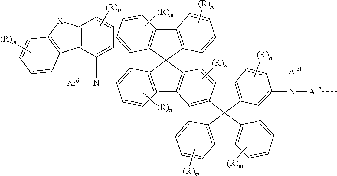
- structural units of formulae (XI) and (XII) are selected from the structural units of the following formulae (XIa) and (XIIa):
- Ar 6 , Ar 7 , Ar 8 , Ar 9 , R, m, n and X can adopt the meaning indicated above, in particular for formulae (I), (Ia), (Ib), (VIIIa) and/or (VIIIb).
- Ar 6 , Ar 7 , Ar 8 , R, m, n and p can adopt the meaning indicated above, in particular for formulae (I), (Ia), (Ib), (VIIIa) and/or (VIIIb), and o is 0, 1 or 2.
- the structural units of formulae (XIII) and (XIV) are selected from the structural formulae of the following formulae (XIIIa) and (XIVa):
- Ar 6 , Ar 7 , Ar 8 , Ar 9 , R, m, n and X can adopt the meaning indicated above, in particular for formulae (I), (Ia), (Ib), (VIIIa) and/or (VIIIb).
- Ar 6 , Ar 7 , Ar 8 , R, m, n and p can adopt the meaning indicated above, in particular for formulae (I), (Ia), (Ib), (VIIIa) and/or (VIIIb) and, o is 0, 1 oder 2.
- the structural units of formulae (IXa) and (Xa) are selected from the structural units of the following formulae (IXb) and (Xb):
- Ar 9 , R, m and p can adopt the meaning indicated above, in particular for formulae (I), (Ia), (Ib), (VIIIa) and/or (VIIIb).
- R, m, n and p can adopt the meaning indicated above, in particular for formulae (I), (Ia), (Ib), (VIIIa) and/or (VIIIb) and, o is 0, 1 or 2.
- the structural units of formulae (XIa) and (XIIa) are selected from the structural units of the following formulae (XIb) and (XIIb):
- Ar 9 , R, X, m, n and p can adopt the meaning indicated above, in particular for formulae (I), (Ia), (Ib), (VIIIa) and/or (VIIIb).
- R, X, m, n and p can adopt the same meaning indicated above, in particular for formulae (I), (Ia), (Ib), (VIIIa) and/or (VIIIb), and o is 0, 1 or 2.
- structural units of formulae (XIIa) and (XIVa) are selected from the structural units of the following formulae (XIIIb) and (XIVb):
- R, X, m, n and p can adopt the meaning indicated above, in particular for formulae (I), (Ia), (Ib), (VIIIa) and/or (VIIIb).
- R, X, m, n and p can adopt the meaning indicated above, in particular for the formulae (I), (Ia), (Ib), (VIIIa) and/or (VIIIb), and o is 0, 1 or 2.
- the dashed lines represent bonds to adjacent structural units in the polymer. They can be, independently from each other, identically or differently, in ortho-, meta- or para-position, preferably identically in ortho-, meta- or para-position, more preferably in meta- or para-position and most preferably in para-position.
- a “crosslinkable group Q” is a functional group, which is able to react and to form a non-soluble bond.
- the reaction can take place with a further, identical group Q, a further, different group Q or any other part of the same or of another polymer chain.
- Crosslinkable groups are this reactive groups.
- the result of the reaction of the crosslinkable groups is a corresponding crosslinked compound.
- the chemical reaction can also take place in the layer, where an unsoluble layer is produced as a result.
- the crosslinking can usually be supported with heat or with UV-, microwave-, X-Ray- or electron radiation, optionally in the presence of an initiator.
- Unsoluble in the context of the present invention means preferably, that the polymer according to the present invention exhibits, after the crosslinking reaction, thus after the reaction of the crosslinkable groups, a solubility at room temperature in an organic solvent, which is at least reduced with a factor 3, preferably with a factor 10, in comparison with the corresponding non-crosslinked polymer of the invention in the same organic solvent.
- At least one crosslinkable group means that one structural unit has one or more crosslinkable groups.
- One structural unit preferably has exactly one crosslinkable group.
- the structural unit of formula (I) has a crosslinkable group
- this group can be linked to Ar 1 , Ar 2 or Ar 3 .
- the crosslinkable group is linked to the monovalent linked, mono- or polycyclic, aromatic or heteroaromatic Ar 3 .
- a structural unit of formulae (VIIIa) or (VIIIb) has a crosslinkable group, then this group can be linked to Ar 5 , Ar 6 , Ar 7 , Ar 8 or Ar 9 .
- the crosslinkable group is preferably linked to one of the monovalent linked, mono- or polycyclic, aromatic or heteroaromatic ring system, that is Ar 5 or Ar 6 .
- R in formulae E1 to E12 can adopt the meaning indicated above for formula (I)
- X can adopt the meaning indicated for formulae (Ia) and/or (Ib)
- R in formulae M1 to M23 can adopt the meaning indicated for formula (I)
- X can adopt the meaning indicated for formulae (Ia) and/or (Ib).
- Y can be CR 2 , SiR 2 , O, S, a straight or branched alkyl group having 1 to 20 C atoms, or an alkenyl or alkynyl group having 2 to 20 C atoms, which may in each case be substituted by one or more radicals R 1 , where one or more non-adjacent CH 2 groups may be replaced by S 1 (R 1 ) 2 , C ⁇ O, C ⁇ S, C ⁇ NR 1 , P( ⁇ O)(R 1 ), SO, SO 2 , NR 1 , O, S or CONR 1 or an aromatic or heteroaromatic ring system having 5 to 60 aromatic ring atoms, which may in each case be substituted by one or more radicals R 1 , or an aryloxy or heteroaryloxy group having 5 to 60 aromatic ring atoms, which may be substituted by one or more radicals R 1 , or an aralkyl or heteroaralkyl group having 5 to 60 aromatic ring atoms, which may be substitute
- indices have the following meaning:
- n 0, 1, 2, 3 or 4;
- n 0, 1, 2 or 3;
- R in formulae E1a to E12a can adopt the same meaning as indicated for formula (I).
- indices have the following meaning:
- n 0, 1, 2 or 3.
- R in formulae M1a to M23b can adopt the meaning indicated for formula (I)
- X can adopt the meaning indicated for formulae (Ia) and/or (Ib).
- Y can be CR 2 , SiR 2 , O, S, a straight alkyl group having 1 to 10 C atoms, or an alkenyl or alkynyl group having 2 to 10 C atoms, which may in each case be substituted by one or more radicals R 1 , where one or more non-adjacent CH 2 groups, CH-groups or C atoms of the alkyl, alkenyl or alkinyl group group may be replaced by S 1 (R 1 ) 2 , C ⁇ O, C ⁇ NR 1 , P( ⁇ O)(R 1 ), NR 1 , O, CONR 1 or an aromatic or heteroaromatic ring system having 5 to 30 aromatic ring atoms, which may in each case be substituted by one or more radicals R 1 , or an aryloxy or heteroaryloxy group having 5 to 30 aromatic ring atoms, which may be substituted by one or more radicals R 1 , or an aralkyl or heteroaralkyl group having 5 to 30
- indices have the following meaning:
- n 0, 1, 2, 3 or 4;
- n 0, 1, 2 or 3;
- o 0, 1 or 2.
- the concentration of the polymer in the formulation according to the invention is preferably in the range of from 10 g/l to 100 g/l, more preferably 15 g/l to 80 g/l, and most preferably 20 g/l to 60 g/l, based on the total formulation.
- the organic semiconductor according to the invention is a low-molecular hole-transport material and/or hole-injection material having a molecular weight of ⁇ 5000 g/mol, preferably ⁇ 3000 g/mol, and more preferably ⁇ 2000 g/mol.
- the low molecular hole-transport material and/or hole-injection material is a triarylamine compound having three aromatic or heteroaromatic ring systems Ar 1 , Ar 2 , Ar 3 , wherein at least one of Ar 1 , Ar 2 , Ar 3 is substituted by Ar 4 in at least one, preferably in one of the two ortho positions, where Ar 4 is a mono- or polycyclic, aromatic or heteroaromatic ring system having 5 to 60 aromatic ring atoms, which may be substituted by one or more radicals R.
- the triarylamine compound has the following formula (I′):
- Ar 3 according to formula (I′) is in at least one, preferably in one of the two ortho-positions relating to the Nitrogen atom represented in formula (I′), substituted by Ar 4 , where Ar 4 is a mono- or polycyclic, aromatic or heteroaromatic ring system with 5 to 60 aromatic ring atoms, which may be substituted by one or more radical R, where R can adopt the meanings indicated above.
- Ar 4 here may either be linked directly, i.e. via a single bond, to Ar, or alternatively via a linking group X.
- the compound of formula (I) thus preferably has the following formula (Ia′).
- the compound of formula (I′) is characterised in that Ar 3 is substituted by Ar 4 in one of the two ortho positions, and Ar 3 is additionally linked to Ar 4 in the meta position that is adjacent to the substituted ortho position.
- the compound of formula (I′) thus preferably has the following formula (Ib′):
- the compound of formula (I′) is selected from the following formulae (II′), (III′) and (IV′):
- the compound of formula (II′) is selected from the following formula (V′):
- the compound of formula (III′) is selected from the following formula (VI′):
- Ar 1 , Ar 2 , R, m and n can adopt the meanings indicated above.
- the compound of formula (IV′) is selected from the following formula (VII′):
- Ar 1 , Ar 2 , R, m and n can adopt the meanings indicated above.
- the compound of formula (V′) is selected from the following formula (Vg′):
- Vg-1′ (Vg-2′) (Vg-3′) (Vg-4′) (Vg-5′) (Vg-6′) (Vg-7′) (Vg-8′)
- R, k, m, n and p can adopt the meanings indicated above.
- the compound of formula (VI′) is selected from the following formula (VIg′):
- R, X, m and n can adopt the meanings indicated above.
- Vg-1′ (VIg-2′) (VIg-3′) (VIg-4′) (VIg-5′) (VIg-6′) (VIg-7′)
- the compound of formula (VII′) is selected from compounds of the following formula (VIIg′):
- R, X, m and n can adopt the meanings indicated above.
- VIIg-1′ (VIIg-2′) (VIIg-3′) where R, m and n can adopt the meanings indicated above.
- the concentration of the polymer in the formulation according to the invention is preferably in the range of from 10 g/l to 100 g/l, more preferably 15 g/l to 80 g/l, and most preferably 20 g/l to 60 g/l, based on the total formulation.
- compositions according to the present invention comprise at least one metal complex.
- the metal complex comprises a metal atom of group 13 to 15 and a ligand of the following structure
- the metal complex is preferably a “p-dopant” material.
- p-dopant materials are materials, which exhibit a lewis-acidity and/or which are able to form a complex with the matrix material, in which these materials act as Lewis-acids (also mention only formal).
- R 13 in formula (L-I) is preferably selected from the group consisting of a straight-chain alkyl, long-chain alkyl, alkoxy, long-chain alkoxy, cycloalkyl, halogenalkyl, aryl, arylene, halogenoaryl, heteroaryl, heteroarylene, heterocycloalkylene, heterocycloalkyl, halogenoheteroaryl, alkenyl, halogenalkenyl, alkinyl, halogenalkinyl, ketoaryl, halogenoketoaryl, ketoheteroaryl, ketoalkyl, halogenoketoalkyl, ketoalkenyl, or halogenketoalkenyl, which preferably have 1 to 40 C atoms, more preferably 1 to 20 C atoms, where in each case one or more non-adjacent CH 2 groups may be replaced by —O—, —S—, —NH—, —NR—, —SiR 2
- a long-chain alkyl group considering the description of R 11 , R 12 and R 13 according to formula (L-I), preferably has 5 to 20 C atoms. Further considering the description of R 11 , R 12 and R 13 , alkyl groups where it is not precised that they are “long-chain”, can preferably have 1 to 10, more preferably 1 to 4 C atoms.
- metal atom of group 13 to 15 refer to metals of the 13. to 15. group according to IUPAC, that is, aluminum, gallium, indium, silicon, germanium, tin, lead, thallium, arsenic, antimony, bismuth or mixtures thereof.
- metals of groups 14 and 15 that is, silicon, germanium, tin, lead, arsenic, antimony, bismuth, more preferably tin and/or bismuth, most preferably bismuth.
- the metal atom of the metal complex according to the invention is selected from the group consisting of bismuth, tin or mixtures thereof, where bismuth is particularly preferred.
- the metal complex is a mono- or bi- or polynuclear metal complex. More particularly, the metal complex can, in solid state, be present as a polynuclear metal complex.
- At least one of ligand L is bridged to two metal atoms.
- M Metal atom
- L ligand
- m 1 to 10 and for the case that m>1, all L are independent from each others.
- metal complexes are particularly preferred for tin and Bismuth; in this case, m is preferably equal to 2 for tin and respectively 2.4 and 3 or 5 for bismuth depending on the oxidation state.
- M metal atom
- L ligand
- L′ ligand different from L selected from the group consisting of aryl, heteroaryl, halogenoaryl and halogenoheteroaryl groups, where n is from 0 to 3 and in the case that n>1, each L′ is selected independently from each other.
- n is from 0 to 3 and in the case that n>1, each L′ is selected independently from each other.
- the metal complex comprises bismuth as a metal atom. Particular preference is given to bismuth-metal complexes of:
- a possible metal complex is a metal complex of formula (L-1), in which R 13 has at least one substituent, which is selected from halogens, pseudohalogens, —CN, —NO 2 .
- a metal complex according to the invention is a metal complex of formula (L-I), in which R 13 corresponds to one of the following formula (R 13 -I), (R 13 -II) or (R 13 -III) as depicted below:
- Y 1 to Y 7 are, on each occurrence, independently from each other, selected from the group consisting of C—F, C—CF 3 , C—NO 2 , C—CN, C-halogen, C-pseudohalogen or N and the dashed lines represent the connecting sites.
- R 13 is selected from the group consisting of halogenated, preferably perhalogenated and/or pseudohalogenated pteridine, isopteridine, napthyridine, quinoxaline, azaquinoxaline.
- R 13 can further correspond to one of the following structures of the following formulae:
- the metal complex is a lewis-acid (without the presence of matrix material), that is, the metal complex acts as an electron pair acceptor. This is particularly adapted for the interaction with the matrix material.
- the metal complex (without the presence of a matrix material) has at least one open or at least partly accessible coordination site. This is also particularly adapted for the interaction with the matrix material.
- R 13 is selected from the group consisting in halogenoalkyl groups, preferably perfluoralkyl with 1 to 8 C atoms, more preferably 1 to 4 C atoms, halogenoaryl, preferably perfluoraryl, halogenoalkylaryl, preferably perfluoralkylaryl and halogenheteroaryl, preferably perfluorheteroaryl, where these groups preferably have 6 to 20 C atoms.
- the metal complex can further comprise a ligand L, which is selected from the group consisting of non-substituted, partially fluorinated or perfluorinated organic carboxylic acids
- preferred ligands L are fluorinated benzoic acids like 2-(trifluoromethyl) benzoic acid; 3,5-difluorobenzoic acid; 3-hydroxy-2,4,6-triiodobenzoic acid; 3-fluoro-4-methylbenzoic acid; 3-(trifluoromethoxy)benzoic acid; 4-(trifluoromethoxy)benzoic acid; 4-chloro-2,5-difluorobenzoic acid; 2-chloro-4,5-difluorobenzoic acid; 2,4,5-trifluorobenzoic acid; 2-fluorobenzoic acid; 4-fluorobenzoic acid; 2,3,4-trifluorobenzoic acid; 2,3,5-trifluorobenzoic acid; 2,3-difluorobenzoic acid; 2,4-bis(trifluoromethyl)benzoic acid; 2,4-difluorobenzoic acid; 2,5-difluorobenzoic acid; 2,6-bis(trifluoromethyl)benzoic acid; 2,6-bis(
- metal complexes like Bi(O 2 CCF 3 ) 3 , Bi(O 2 CC 6 H 2 (2, 3, 4-F 3 )) 3 and Bismuth-tris-pentafluorobenzoate.
- the concentration of the of the metal complex according to the invention can be in the range of from 5 g/l to 100 g/l, preferably 7.5 g/l to 80 g/l, and more preferably 10 g/to 60 g/l, based on the total formulation.
- the weight ratio of the semiconductor to the metal complex in the formulation of the invention is from 1000:1 to 1:2, preferably from 400:1 to 1:1, more preferably from 100:1 to 3:2 and most preferably from 20:1 to 2:1.
- the amount of metal complex to organic semiconductor is preferably from 0.1 to 70 wt. %, more preferably from 0.25 to 50 wt. %, most preferably from 1 to 40 wt. % and very most preferably from 5 to 30 wt. %, calculated on the total amount of organic semiconductor and metal complex. It is possible to use a higher or lower amount of metal complex, but the performance of the layer obtained from the formulation according to the invention can decrease as a consequence.
- the formulation according to the invention may comprise further additives and processing assistants.
- additives and processing assistants include, inter alia, surface-active substances, surfactants, lubricants and greases, additives which increase the conductivity, dispersants, hydrophobicising agents, adhesion promoters, flow improvers, antifoams, deaerating agents, diluents, which may be reactive or unreactive, fillers, assistants, processing assistants, dyes, pigments, stabilisers, sensitisers, nanoparticles and inhibitors.
- a formulation in accordance with the present invention can be employed for the production of a layer or multilayered structure in which the organofunctional materials are present in layers, as are required for the production of preferred electronic or opto-electronic components, such as OLEDs.
- the formulation of the present invention can preferably be employed for the formation of a functional layer comprising an organic semiconductor and a metal complex on a substrate or on one of the layers applied to the substrate.
- Still further object of the invention is a process for the production of an electronic device with a multilayer structure, wherein at least one layer is obtained from the application of a formulation of the present invention.
- a formulation according to the invention is applied to a substrate and dried.
- the functional layer obtained from the formulation according to the invention can be produced, for example, by flood coating, dip coating, spray coating, spin coating, screen printing, relief printing, gravure printing, rotary printing, roller coating, flexographic printing, offset printing or nozzle printing, preferably ink-jet printing on a substrate or one of the layers applied to the substrate.
- a drying step can be carried out in order to remove the solvent.
- the drying can preferably be carried out at relatively low temperature and over a relatively long period in order to avoid bubble formation and to obtain a uniform coating.
- the drying can preferably be carried out at a temperature in the range from 80 to 300° C., particularly preferably 150 to 250° C. and especially preferably 180 to 200° C.
- the drying here can preferably be carried out at a pressure in the range from 10-mbar to 2 bar, particularly preferably in the range from 10 ⁇ 2 mbar to 1 bar and especially preferably in the range from 10 ⁇ 1 mbar to 100 mbar.
- the duration of the drying depends on the degree of drying to be achieved, where small amounts of water can optionally be removed at relatively high temperature and in combination with sintering, which is preferably to be carried out.
- Another object of the invention is an electronic device obtainable by such a process for the production of an electronic device.
- An electronic device is taken to mean a device which comprises anode, cathode and at least one functional layer in between, where this functional layer comprises at least one organic or organometallic compound.
- the organic, electronic device is preferably an organic electroluminescent device (OLED), a polymeric electroluminescent device (PLED), an organic integrated circuit (O-IC), an organic field-effect transistor (O-FET), an organic thin-film transistor (O-TFT), an organic, light-emitting transistor (O-LET), an organic solar cell (O-SC), an organic, optical detector, an organic photoreceptor, an organic field-quench device (O-FQD), an organic electrical sensor, a light-emitting electrochemical cell (LEC) or an organic laser diode (O-laser). Preference is given to organic electroluminescent device (OLED).
- OLED organic electroluminescent device
- PLED polymeric electroluminescent device
- O-IC organic integrated circuit
- O-FET organic field-effect transistor
- OF-TFT organic thin-film transistor
- O-LET organic, light-emitting transistor
- O-SC organic solar cell
- O-SC organic, optical detector, an organic photoreceptor, an organic
- Part A Organic Semiconductor
- organic semiconductors (OS) used for the formation of the formulations according to the invention are already described in the prior art and were produced according to the literature instructions.
- a formulation here is taken to mean a mixture comprising at least one organic semiconductor, at least one metal complex and at least one solvent.
- the solubility of a material in a solvent is the highest material-to-solvent ratio in which the solution at 20° C. is clear and stays clear for several hours.
- the solubility (g/l) is determined according to the following method:
- a known amount of the solvent for example 100 mL is put in a container
- Step (2) is repeated until some of the material does not dissolve despite a vigorous and prolonged stirring.
- solubilities (in g/l) of the various materials in various solvent at 20° C. are listed in the table below.
- Formulations according to the invention which comprise at least one organic semiconductor, at least one metal complex and at least one solvent, lead to OLEDs which are much easier to produce than OLEDs obtained from vacuum processes, and at the same time still exhibit good properties.
- formulations according to the invention can be used in two different layer sequences:
- Stack A is as follows:
- Stack B is as follows:
- the substrate consists of glass platelets, which are coated with a structured 50 nm thick ITO (indium tin oxide) layer.
- ITO indium tin oxide
- the functional layers are then applied onto the coated substrate according to the structures of Stacks A and B.
- the comparative mixture according to the prior art comprises a solvent consisting of Anisole: Xylene in the ratio 2:1 (LM1).
- LM1 Anisole: Xylene in the ratio 2:1
- the typical solid content of such solutions is about 8-35 g/l, when film thicknesses of between 20 nm and 200 nm have to be achieved by means of spin coating.
- the layers were spin coated in an inert gas atmosphere, in this case argon, and heated for 60 minutes at 180° C. or 220° C.
- the hole transport layer in Stack B is formed by thermal evaporation in a vacuum chamber.
- the materials used in this case are shown in Table D1.
- the emissive layer in Stack B is formed by thermal evaporation in a vacuum chamber.
- the layer may consist of more than one material, which are deposited by means of co-evaporation in a given volume fraction.
- a reference such as MB1:SEB (95%:5%) in this case means that the materials MB1 and SEB are present in the layer in a volume fraction of 95%:5%.
- the materials for the electron-transport layer are also thermally evaporated in a vacuum chamber and are shown in Table D3.
- the electron-transport layer consists of the two materials ETM1 and ETM2, which are deposited by means of co-evaporation in a volume fraction of 50%:50%.
- the cathode is formed by the deposition of a 100 nm thick aluminum layer by means of thermal evaporation.
- the OLEDs are characterized by standard methods. For this purpose, the electroluminescence spectra, the current-voltage-luminance characteristics (IUL characteristics), assuming a Lambertian radiation pattern and in the case of Stack B, the operating lifetime are determined. Data like the operating voltage (in V) and the external quantum efficiency (in %) at a certain brightness are determined from the IUL characteristics.
- LD80@4000 cd/m 2 corresponds to the lifetime until which the brightness of the OLED drops from an initial brightness of 4000 cd/m 2 to a brightness equal to 80% of the initial intensity, i.e. at 3600 cd m 2 .
- Table D5a shows results of hole-dominated components according to Stack A. In such components, the current is dominated by holes, which is why no recombination with electrons takes place that would lead to luminescence.
- Table D5b shows that the use of formulations according to the invention leads to OLEDs with a good lifetime and efficiency.
Landscapes
- Engineering & Computer Science (AREA)
- Chemical & Material Sciences (AREA)
- Materials Engineering (AREA)
- Physics & Mathematics (AREA)
- Manufacturing & Machinery (AREA)
- Inorganic Chemistry (AREA)
- Spectroscopy & Molecular Physics (AREA)
- Optics & Photonics (AREA)
- Electroluminescent Light Sources (AREA)
- Compositions Of Macromolecular Compounds (AREA)
Abstract
Description
- (1) A known amount of the solvent (for example 100 mL) is put in a container;
- (2) A defined amount of the material is added and the mixture is stirred with a magnetic stirring bar;
- (4) Step (2) is repeated until some of the material does not dissolve despite a vigorous and prolonged stirring.
HOMO(eV)=((HEh*27.212)−0.9899)/1.1206
LUMO(eV)=((LEh*27.212)−2.0041)/1.385

where
-
- Ar1 to Ar3 is on each occurrence, in each case identically or differently, a mono- or polycyclic, aromatic or heteroaromatic ring system having 5 to 60 aromatic ring atoms, which may be substituted by one or more radicals R;
- R is on each occurrence, identically or differently, H, D, F, Cl, Br, I, N(R1)2, CN, NO2, S1(R1)3, B(OR1)2, C(═O)R1, P(═O)(R1)2, S(═O)R1, S(═O)2R1, OSO2R1, a straight-chain alkyl, alkoxy or thioalkoxy group having 1 to 40 C atoms or a branched or cyclic alkyl, alkoxy or thioalkoxy group having 3 to 40 C atoms, each of which may be substituted by one or more radicals R1, where one or more non-adjacent CH2 groups may be replaced by R1C═CR1, C≡C, S1(R1)2, C═O, C═S, C═NR1, P(═O)(R1), SO, SO2, NR1, O, S or CONR1 and where one or more H atoms may be replaced by D, F, Cl, Br, I or CN, or a mono- or polycyclic, aromatic or heteroaromatic ring system having 5 to 60 aromatic ring atoms, which may in each case be substituted by one or more radicals R1, or an aryloxy or heteroaryloxy group having 5 to 60 aromatic ring atoms, which may be substituted by one or more radicals R1, or an aralkyl or heteroaralkyl group having 5 to 60 aromatic ring atoms, which may be substituted by one or more radicals R1, or a diarylamino group, diheteroarylamino group or arylheteroarylamino group having 10 to 40 aromatic ring atoms, which may be substituted by one or more radicals R1, or a crosslinkable group Q, where two or more radicals R may also form a mono- or polycyclic, aliphatic, aromatic and/or benzo-fused ring system with one another;
- R1 is on each occurrence, identically or differently, H, D, F or an aliphatic hydrocarbon radical having 1 to 20 C atoms, an aromatic and/or a heteroaromatic hydrocarbon radical having 5 to 20 C atoms, in which, in addition, one or more H atoms may be replaced by F; where two or more substituents R1 may also form a mono- or polycyclic, aliphatic or aromatic ring system with one another; and
the dashed lines represent bonds to adjacent structural units in the polymer,
and where at least one of Ar1, Ar2 and/or Ar3 is substituted by a radical R comprising at least 2 C atoms, preferably at least 4 C atoms and more preferably at least 6 C atoms. Advantageously, R exhibit a C—C-Doppelbond or R is a part of a mono- or polycyclic, aromatic or heteroaromatic ring system with 5 to 60 aromatic ring atoms.

where Ar1, Ar2, Ar3, Ar4 and R can adopt the meanings indicated above,
q=0, 1, 2, 3, 4, 5 or 6, preferably 0, 1, 2, 3 or 4,
X=CR2, NR, SiR2, O, S, C═O or P═O, preferably CR2, NR, O or S, and
r=0 or 1, preferably 0.

where Ar1, Ar2, Ar3, Ar4 and R can adopt the meanings indicated above,
m=0, 1, 2, 3 or 4,
n=0, 1, 2 or 3,
X=CR2, NR, SiR2, O, S, C═O or P═O, preferably CR2, NR, O or S, and
s and t are each 0 or 1, where the sum (s+t)=1 or 2, preferably 1.

where Ar1, Ar2, Ar and R can adopt the meanings indicated above,
m=0, 1, 2, 3 or 4,
n=0, 1, 2 or 3, and
X=CR2, NR, SiR2, O, S, C═O or P═O, preferably CR2, NR, O or S.

where Ar1, Ar2, R and m can adopt the meanings indicated above, and
p=0, 1, 2, 3, 4 or 5.
 | (Va) | |
 | (Vb) | |
 | (Vc) | |
 | (Vd) | |
 | (Ve) | |
 | (Vf) | |
 | (Vg) | |
 | (Vh) | |
where Ar1, Ar2, R, m, n and p can adopt the meanings indicated above, and
k=0, 1 or 2.

where Ar1, Ar2, R, m and n can adopt the meanings indicated above.
 | (VIa) | |
 | (VIb) | |
 | (VIc) | |
 | (VId) | |
 | (VIe) | |
 | (VIf) | |
where Ar1, Ar2, R, m, n and p can adopt the meanings indicated above.

where Ar1, Ar2, R, m and n can adopt the meanings indicated above.
 | (VIIa) | |
 | (VIIb) | |
 | (VIIc) | |
 | (VIId) | |
 | (VIIe) | |
 | (VIIf) | |
where Ar1, Ar2, R, m, n and p can adopt the meanings indicated above.

where R, m and p can adopt the meanings indicated above.
 | (Vg-1) |
 | (Vg-2) |
 | (Vg-3) |
 | (Vg-4) |
 | (Vg-5) |
 | (Vg-6) |
 | (Vg-7) |
 | (Vg-8) |
where R, k, m, n and p can adopt the meanings indicated above and o is 0, 1 or 2

where R, X, m and n can adopt the meanings indicated above.
 | (VIg-1) | |
 | (VIg-2) | |
 | (VIg-3) | |
 | (VIg-4) | |
 | (VIg-5) | |
 | (VIg-6) | |
 | (VIg-7) | |
where R, m, n and p can adopt the meanings indicated above, and
v=1 to 20, preferably 1 to 10.

where R, X, m and n can adopt the meanings indicated above.
 | (VIIg-1) | |
 | (VIIg-2) | |
 | (VIIg-3) | |
where R, m and n can adopt the meanings indicated above.

or from structural units of the following formula (VIIb):

where w is 1, 2 or 3, Ar5 to Ar9 is on each occurrence, in each case identically or differently, a mono- or polycyclic, aromatic or heteroaromatic ring system having 5 to 60 aromatic ring atoms, which may be substituted by one or more radicals R; where R can adopt the meaning indicated in formula (I); the dashed lines represent bonds to adjacent structural units in the polymer; and at least one of Ar5 to Ar9 is substituted by a radical R comprising at least 2 C atoms, preferably at least 4 C atoms and more preferably at least 6 C atoms.

where Ar4, Ar5, Ar6, Ar7, Ar8, Ar9, X, m, n, r, s, t and R can adopt the meaning indicated above, in particular for formulae (I), (Ia), (Ib), (VIIIa) and/or (VIIIb).

where Ar4, Ar5, Ar8, Ar7, Ar8, Ar9, X, m, n, s, t and R can adopt the meaning indicated above, in particular for formulae (I), (Ia), (Ib), (VIIIa) and/or (VIIIb).

Ar4, Ar5, Ar6, Ar7, Ar6, Ar9, X, m, n, p, R and the dashed lines can adopt the meaning indicated above, in particular for formulae (I), (Ia), (Ib), (VIIIa) and/or (VIIIb).

where Are, Ar7, Ar, Ar9, R, m, p and the dashed lines can adopt the meaning indicated above, in particular for formulae (I), (Ia), (Ib), (VIIIa) and/or (VIIIb).
 |
 |
 |
 |
 |
 |
 |
 |
 |
 |
 |
 |
 |
 |
 |
 |
 |
 |
 |
 |
 |
 |
 |
 |
 |
 |
 |
 |
 |
 |
 |
 |
 |
 |
where Ar6, Ar7, Ar8, R, m, n, p and the dashed lines can adopt the meaning indicated above, in particular for formulae (I), (Ia), (Ib), (VIIIa) and/or (VIIIb), and o is 0, 1 or 2.

where Ar6, Ar7, Ar8, Ar9, R, m, n and X can adopt the meaning indicated above, in particular for formulae (I), (Ia), (Ib), (VIIIa) and/or (VIIIb).
 |
 |
 |
 |
 |
 |
 |
 |
 |
 |
 |
 |
 |
 |
 |
 |
 |
 |
 |
 |
 |
 |
 |
 |
 |
 |
 |
 |
 |
 |
 |
 |
where Ar6, Ar7, Ar8, R, m, n and p can adopt the meaning indicated above, in particular for formulae (I), (Ia), (Ib), (VIIIa) and/or (VIIIb), and o is 0, 1 or 2.

where Ar6, Ar7, Ar8, Ar9, R, m, n and X can adopt the meaning indicated above, in particular for formulae (I), (Ia), (Ib), (VIIIa) and/or (VIIIb).
 |
 |
 |
 |
 |
 |
 |
 |
 |
 |
 |
 |
 |
 |
 |
 |
 |
 |
 |
 |
 |
 |
 |
 |
 |
 |
 |
 |
 |
 |
 |
 |
 |
 |
where Ar6, Ar7, Ar8, R, m, n and p can adopt the meaning indicated above, in particular for formulae (I), (Ia), (Ib), (VIIIa) and/or (VIIIb) and, o is 0, 1 oder 2.

where Ar9, R, m and p can adopt the meaning indicated above, in particular for formulae (I), (Ia), (Ib), (VIIIa) and/or (VIIIb).
 |
 |
 |
 |
 |
 |
 |
 |
 |
 |
 |
 |
 |
where R, m, n and p can adopt the meaning indicated above, in particular for formulae (I), (Ia), (Ib), (VIIIa) and/or (VIIIb) and, o is 0, 1 or 2.

where Ar9, R, X, m, n and p can adopt the meaning indicated above, in particular for formulae (I), (Ia), (Ib), (VIIIa) and/or (VIIIb).
 |
 |
 |
 |
 |
 |
 |
 |
 |
 |
 |
 |
 |
where R, X, m, n and p can adopt the same meaning indicated above, in particular for formulae (I), (Ia), (Ib), (VIIIa) and/or (VIIIb), and o is 0, 1 or 2.

where R, X, m, n and p can adopt the meaning indicated above, in particular for formulae (I), (Ia), (Ib), (VIIIa) and/or (VIIIb).
 |
 |
 |
 |
 |
 |
 |
 |
 |
 |
 |
 |
 |
where R, X, m, n and p can adopt the meaning indicated above, in particular for the formulae (I), (Ia), (Ib), (VIIIa) and/or (VIIIb), and o is 0, 1 or 2.


where R in formulae E1 to E12 can adopt the meaning indicated above for formula (I), X can adopt the meaning indicated for formulae (Ia) and/or (Ib), and the indices have the following meaning:
m=0, 1, 2, 3 or 4;
n=0, 1, 2 or 3;
o=0, 1 or 2; and
p=0, 1, 2, 3, 4 or 5.


R in formulae M1 to M23 can adopt the meaning indicated for formula (I), X can adopt the meaning indicated for formulae (Ia) and/or (Ib).


R in formulae E1a to E12a can adopt the same meaning as indicated for formula (I).


R in formulae M1a to M23b can adopt the meaning indicated for formula (I), X can adopt the meaning indicated for formulae (Ia) and/or (Ib).

where the symbols and indices can adopt the same meaning as for formula (I).

where Ar1, Ar2, Ar3, Ar4 and R can adopt the meanings indicated above,
q=0, 1, 2, 3, 4, 5 or 6, preferably 0, 1, 2, 3 or 4,
X=CR2, NR, SiR2, O, S, C═O or P═O, preferably CR2, NR, O or S, and
r=0 or 1, preferably 0.

where Ar1, Ar2, Ar3, Ar4 and R can adopt the meanings indicated above,
m=0, 1, 2, 3 or 4,
n=0, 1, 2 or 3,
X=CR2, NR, SiR2, O, S, C═O or P═O, preferably CR2, NR, O or S, and
s and t are each 0 or 1, where the sum (s+t)=1 or 2, preferably 1.

where Ar1, Ar2, Ar4 and R can adopt the meanings indicated above,
m=0, 1, 2, 3 or 4,
n=0, 1, 2 or 3, and
X=CR2, NR, SiR2, O, S, C═O or P═O, preferably CR2, NR, O or S.

where Ar1, Ar2, R and m can adopt the meanings indicated above, and
p=0, 1, 2, 3, 4 or 5.
 | (Va′) | ||
 | (Vb′) | ||
 | (Vc′) | ||
 | (Vd′) | ||
 | (Ve′) | ||
 | (Vf′) | ||
 | (Vg′) | ||
 | (Vh′) | ||
where Ar1, Ar2, R, m, n and p can adopt the meanings indicated above, and
k=0, 1 or 2.

where Ar1, Ar2, R, m and n can adopt the meanings indicated above.
 | (VIa′) | ||
 | (VIb′) | ||
 | (VIc′) | ||
 | (VId′) | ||
 | (VIe′) | ||
 | (VIf′) | ||
where Ar1, Ar2, R, m, n and p can adopt the meanings indicated above.

where Ar1, Ar2, R, m and n can adopt the meanings indicated above.
 | (VIIa′) | ||
 | (VIIb′) | ||
 | (VIIc′) | ||
 | (VIId′) | ||
 | (VIIe′) | ||
 | (VIIf′) | ||
where Ar1, Ar2, R, m, n and p can adopt the meanings indicated above.

where R, m and p can adopt the meanings indicated above.
 | (Vg-1′) |
 | (Vg-2′) |
 | (Vg-3′) |
 | (Vg-4′) |
 | (Vg-5′) |
 | (Vg-6′) |
 | (Vg-7′) |
 | (Vg-8′) |
where R, k, m, n and p can adopt the meanings indicated above.

where R, X, m and n can adopt the meanings indicated above.
 | (VIg-1′) | ||
 | (VIg-2′) | ||
 | (VIg-3′) | ||
 | (VIg-4′) | ||
 | (VIg-5′) | ||
 | (VIg-6′) | ||
 | (VIg-7′) | ||
where R, m, n and p can adopt the meanings indicated above, and
v=1 to 20, preferably 1 to 10.

where R, X, m and n can adopt the meanings indicated above.
 | (VIIg-1′) |
 | (VIIg-2′) |
 | (VIIg-3′) |
where R, m and n can adopt the meanings indicated above.

-
- where
- R11 and R12 are selected, identically or differently, from the group consisting of O, S, Se, NH or NR14, where R14 is an alkyl or aryl group having preferably 1 to 40 C atoms, ore preferably 1 to 20 C atoms and most preferably 1 to 12 C atoms; where R14 and R13 may form a ring with one other; and
- R13 is selected from the group consisting of a straight-chain alkyl, alkoxy or thioalkyl group having 1 to 40 C atoms or an alkenyl or alkinyl group having 2 to 40 C atoms or a branched or cyclic alkyl, alkoxy or thioalkyl group having 3 to 40 C atoms, each of which may be substituted by one or more radicals R1, where in each case one or more non-adjacent CH2 groups may be replaced by R1C═CR1, C≡C, S1(R1)2, C═O, C═S, C═NR1, P(═O)(R1), SO, SO2, NR1, O, S or CONR1 and where one or more H atoms may be replaced by D, F, Cl, Br, I or CN, an aromatic or heteroaromatic ring system having 5 to 60 aromatic ring atoms, which may in each case be substituted by one or more radicals R1, an aryloxy or heteroaryloxy group having 5 to 60 aromatic ring atoms, which may be substituted by one or more radicals R1, or an aralkyl or heteroaralkyl group having 5 to 60 aromatic ring atoms, which may in each case be substituted by one or more radicals R1, or a diarylamino group, diheteroarylamino group or arylheteroarylamino group having 10 to 40 aromatic ring atoms, which may be substituted by one or more radicals R1; where R13 may form a ring with at least one of the radical R12; and
- R1 is on each occurrence, identically or differently, H, D, F or an aliphatic hydrocarbon radical having 1 to 20 C atoms, an aromatic and/or a heteroaromatic hydrocarbon radical having 5 to 20 C atoms, in which, in addition, one or more H atoms may be replaced by F; where two or more substituents R1 may also form a mono- or polycyclic, aliphatic or aromatic ring system with one another.
-
- Oxidation stage II, which can exhibit—without wishing to be bound by theory—a paddle-wheel structure as a function of the selected ligand.
- Oxidation stage III, (MLn=3), which can not exhibit—without wishing to be bound by theory—a paddle-wheel structure. These compounds are generally mono- or polynuclear compounds in solid state.
- Oxidation stage V, where a preferred form of the bismuth-metal complex of oxidation stage V corresponds to the form described in WO 2013/182389 A2.

where Y1 to Y7 are, on each occurrence, independently from each other, selected from the group consisting of C—F, C—CF3, C—NO2, C—CN, C-halogen, C-pseudohalogen or N and the dashed lines represent the connecting sites.

where the dashed lines represent the connecting sites.
-
- a. Preparing a first solution comprising at least one solvent and at least one metal complex and
- b. Preparing a second solution comprising at least one solvent and at least one organic semiconductor and
- c. Mixing the first solution obtained in step a) and the second solution obtained in step b) in a specific ratio and forming a formulation by a physical method.
| Organic | ||
| semi- | Synthesis | |
| con- | according | |
| ductors | Structure | to |
| OS1 |  | WO2003/ 048225 WO2010/ 097155 |
| OS2 |  | WO2003/ 048225 |
| OS3 |  | WO2003/ 048225 |
| OS4 |  | WO2003/ 048225 WO2010/ 097155 |
| OS5 |  | WO2003/ 048225 |
| OS6 |  | WO2012- 034627 |
Part B: Metal Complex
| Metal | Synthesis | |
| complex | Structure | according to |
| M1 |  | WO 2013/182389 |
Part C: Formulation
| Material | ||
| Solvent | OS3 | M1 | OS5 | OS6 | |
| LM1 | Anisole:Xylene | >20 g/l | <7.5 | g/l | >20 g/l | >50 g/l |
| (2:1) | ||||||
| LM2 | Anisole | >20 g/l | <7.5 | g/l | >20 g/l | 100 g/l |
| LM3 | Xylene | >20 g/l | <7.5 | g/l | >20 g/l | 40 g/l |
| LM4 | Chlorobenzene | >20 g/l | <7.5 | g/l | >20 g/l | |
| LM5 | THF | >40 g/l | >100 | g/l | >40 g/l | >40 g/l |
| LM6 | Toluene:THF | >50 g/l | >30 | g/l | >50 g/l | >50 g/l |
| (9:1) | ||||||
| LM7 | Hexafluorobenzene | 10 g/l | 15-20 | g/l | ||
| LM8 | Toluene: | 40 g/l | 15 | g/l | 40 g/l | 30 g/l |
| Hexafluorobenzene | ||||||
| (7:3) | ||||||
| LM9 | Meta- | >20 g/l | <7.5 | g/l | >20 g/l | |
| difluorobenzene | ||||||
| LM10 | Fluorobenzene | >30 g/l | <7.5 | g/l | >30 g/l | |
| LM11 | Acetonitrile | <5 g/l | <10 | g/l | <5 g/l | |
| LM12 | Benzonitrile | >20 | g/l | |||
| LM13 | Acetone | <5 g/l | >20 | g/l | <5 g/l | |
| LM14 | DMF | <2 g/l | >40 | g/l | <2 g/l | 10 g/l |
| LM15 | Toluene:DMF | 30 g/l | 15 | g/l | 30 g/l | 25 g/l |
| (8:2) | ||||||
| LM16 | DMSO | <2 g/l | >20 | g/l | <2 g/l | 10 g/l |
| LM17 | Methanol | <5 g/l | >20 | g/l | <5 g/l | |
| LM18 | Toluene:Methanol | 35 g/l | 20 | g/l | 35 g/l | 30 g/l |
| (8:2) | ||||||
| LM19 | EGDME | <5 g/l | >20 | g/l | <5 g/l | |
| LM20 | Toluene | >40 g/l | <7.5 | g/l | >40 g/l | 60 g/l |
Part D: Device Examples
-
- Substrate,
- ITO (50 nm),
- Hole injection layer (HIL) (200 nm),
- Cathode.
-
- Substrate,
- ITO (50 nm),
- HIL (150 nm),
- Hole transport layer (HTL) (40 nm)
- Emissive layer (EML) (30 nm)
- Electron transport layer (ETL) (20 nm),
- Cathode.
| TABLE D1 |
| Structural formula of the hole-transport material (vacuum processed) |
 |
HT1 |
| TABLE D2 |
| Structural formulae of the materials used in the emissive layer |
 |
MB1 |
 |
SEB |
| TABLE D3 |
| Structural formulae of the materials used in the hole-blocking and/or |
| electron-transport layers |
 |
ETM1 |
 |
ETM2 |
| TABLE D4 |
| Structure of the OLEDs |
| HIL | ||||||||
| weight | ||||||||
| metal complex | ratio | T | HTL | EML | ||||
| Ex. | Stack | OS | (M) | (OS:M) | solvent | [° C.] | material | composition |
| D1 | B | OS4 | M1 | 85:15 | LM6 | 180 | HT1 | MB1 95% |
| SEB 5% | ||||||||
| D2 | A | OS5 | M1 | 70:30 | LM1 | 180 | — | — |
| D3 | A | OS1 | M1 | 70:30 | LM1 | 180 | — | — |
| D4 | A | OS5 | M1 | 70:30 | LM6 | 180 | — | — |
| D5 | A | OS1 | M1 | 70:30 | LM6 | 180 | — | — |
| D6 | A | OS6 | M1 | 70:30 | LM6 | 180 | — | — |
| D7 | A | OS3 | M1 | 70:30 | LM8 | 180 | — | — |
| D8 | A | OS4 | M1 | 85:15 | LM15 | 220 | — | — |
| D9 | A | OS2 | M1 | 85:15 | LM18 | 180 | — | — |
| TABLE D5a | ||
| Current | ||
| density at U = | ||
| 3 V | Scattering | |
| Ex. | [mA/cm2] | parameter |
| D2 | 33 | 1.1 |
| D3 | 1 | 0.9 |
| D4 | 24 | 0.2 |
| D5 | 2 | 0.1 |
| D6 | 36 | 0.2 |
| D7 | 39 | 0.4 |
| D8 | 5 | 0.2 |
| D9 | 19 | 0.3 |
| TABLE D5b | |||||
| Efficiency at | Voltage at | LD80 at | |||
| 1000 cd/m2 | 1000 cd/m2 | 4000 cd/m2 | |||
| Ex. | % EQE | [V] | [h] | ||
| D1 | 7.7 | 4.5 | 420 | ||
Claims (16)


Applications Claiming Priority (4)
| Application Number | Priority Date | Filing Date | Title |
|---|---|---|---|
| EP15001556 | 2015-05-22 | ||
| EP15001556.8 | 2015-05-22 | ||
| EP15001556 | 2015-05-22 | ||
| PCT/EP2016/000739 WO2016188609A1 (en) | 2015-05-22 | 2016-05-04 | Formulation containing an organic semiconductor and a metal complex |
Publications (2)
| Publication Number | Publication Date |
|---|---|
| US20190074453A1 US20190074453A1 (en) | 2019-03-07 |
| US10566550B2 true US10566550B2 (en) | 2020-02-18 |
Family
ID=53283951
Family Applications (1)
| Application Number | Title | Priority Date | Filing Date |
|---|---|---|---|
| US15/576,535 Expired - Fee Related US10566550B2 (en) | 2015-05-22 | 2016-05-04 | Formulation containing an organic semiconductor and a metal complex |
Country Status (7)
| Country | Link |
|---|---|
| US (1) | US10566550B2 (en) |
| EP (1) | EP3298639B1 (en) |
| JP (1) | JP6786523B2 (en) |
| KR (1) | KR20180011252A (en) |
| CN (1) | CN107667439B (en) |
| TW (1) | TW201711245A (en) |
| WO (1) | WO2016188609A1 (en) |
Cited By (2)
| Publication number | Priority date | Publication date | Assignee | Title |
|---|---|---|---|---|
| US11787965B2 (en) | 2017-03-30 | 2023-10-17 | Novaled Gmbh | Ink composition for forming an organic layer of a semiconductor |
| US12167687B2 (en) | 2018-04-24 | 2024-12-10 | Samsung Display Co., Ltd. | Organic light-emitting device and method of manufacturing the same |
Families Citing this family (4)
| Publication number | Priority date | Publication date | Assignee | Title |
|---|---|---|---|---|
| US11261291B2 (en) | 2016-12-22 | 2022-03-01 | Merck Patent Gmbh | Materials for electronic devices |
| CN117440703A (en) * | 2017-03-01 | 2024-01-23 | 默克专利有限公司 | Organic electroluminescent devices |
| EP3462516A1 (en) * | 2017-10-02 | 2019-04-03 | Novaled GmbH | Electronic device and method for preparing the same |
| KR102550692B1 (en) * | 2018-04-24 | 2023-07-04 | 삼성디스플레이 주식회사 | Organic light emitting device and method manufacturing the same |
Citations (10)
| Publication number | Priority date | Publication date | Assignee | Title |
|---|---|---|---|---|
| US20120273736A1 (en) | 2009-12-23 | 2012-11-01 | Merck Patent Gmbh | Compositions comprising polymeric binders |
| WO2014048542A1 (en) | 2012-09-27 | 2014-04-03 | Merck Patent Gmbh | Materials for organic electroluminescent devices |
| US20140138661A1 (en) * | 2011-07-11 | 2014-05-22 | Merck Patent Gmbh | Compounds for organic electroluminescent devices |
| CN104245784A (en) | 2012-04-17 | 2014-12-24 | 默克专利有限公司 | Polymers containing substituted oligomeric triarylamine units and electroluminescent devices comprising these polymers |
| US20150123047A1 (en) | 2012-06-06 | 2015-05-07 | Osram Oled Gmbh | Main group metal complexes as p-dopants for organic electronic matrix materials |
| US9090590B2 (en) * | 2009-11-10 | 2015-07-28 | Merck Patent Gmbh | Organic compounds for electroluminescent devices |
| US9090532B2 (en) * | 2008-07-29 | 2015-07-28 | Merck Patent Gmbh | Organic electroluminescent device |
| US9416310B2 (en) * | 2009-09-23 | 2016-08-16 | Merck Patent Gmbh | Materials for electronic devices |
| US9837617B2 (en) * | 2013-08-15 | 2017-12-05 | Merck Patent Gmbh | Materials for electronic devices |
| US9853228B2 (en) * | 2014-07-28 | 2017-12-26 | Merck Patent Gmbh | Metal complexes |
Family Cites Families (11)
| Publication number | Priority date | Publication date | Assignee | Title |
|---|---|---|---|---|
| KR20020025918A (en) * | 2002-02-15 | 2002-04-04 | 박병주 | Organic semiconducting devices and organic electroluminescent devices produced by using wet process |
| DE10249723A1 (en) | 2002-10-25 | 2004-05-06 | Covion Organic Semiconductors Gmbh | Conjugated polymers containing arylamine units, their preparation and use |
| JP2004253371A (en) * | 2003-01-31 | 2004-09-09 | Dainippon Ink & Chem Inc | Organic electroluminescence device |
| KR102189768B1 (en) | 2007-08-08 | 2020-12-14 | 유니버셜 디스플레이 코포레이션 | Single triphenylene chromophores in phosphorescent light emitting diodes |
| DE102007000791A1 (en) * | 2007-09-28 | 2009-04-02 | Universität Köln | Method for producing an organic light-emitting diode or an organic solar cell and produced organic light-emitting diodes or solar cells |
| DE102008033943A1 (en) | 2008-07-18 | 2010-01-21 | Merck Patent Gmbh | New materials for organic electroluminescent devices |
| KR101732199B1 (en) | 2009-02-27 | 2017-05-02 | 메르크 파텐트 게엠베하 | Polymer having aldehyde groups, converting and cross-linking of said polymer, cross-linked polymer, and electroluminescent device comprising said polymer |
| JP2011114322A (en) * | 2009-11-30 | 2011-06-09 | Fujifilm Corp | Charge transporting compound, charge transporting film using the same, organic electroluminescent element, electrophotographic photosensitive member, method for producing charge transporting film, and novel charge transporting compound |
| JP5567407B2 (en) * | 2010-03-15 | 2014-08-06 | ユー・ディー・シー アイルランド リミテッド | Method for manufacturing organic electroluminescent device |
| DE102010045405A1 (en) * | 2010-09-15 | 2012-03-15 | Merck Patent Gmbh | Materials for organic electroluminescent devices |
| US20180006237A1 (en) * | 2015-01-30 | 2018-01-04 | Merck Patent Gmbh | Materials for electronic devices |
-
2016
- 2016-05-04 JP JP2017560978A patent/JP6786523B2/en active Active
- 2016-05-04 WO PCT/EP2016/000739 patent/WO2016188609A1/en not_active Ceased
- 2016-05-04 EP EP16722050.8A patent/EP3298639B1/en not_active Not-in-force
- 2016-05-04 US US15/576,535 patent/US10566550B2/en not_active Expired - Fee Related
- 2016-05-04 CN CN201680029422.9A patent/CN107667439B/en not_active Expired - Fee Related
- 2016-05-04 KR KR1020177037027A patent/KR20180011252A/en not_active Ceased
- 2016-05-18 TW TW105115345A patent/TW201711245A/en unknown
Patent Citations (15)
| Publication number | Priority date | Publication date | Assignee | Title |
|---|---|---|---|---|
| US9090532B2 (en) * | 2008-07-29 | 2015-07-28 | Merck Patent Gmbh | Organic electroluminescent device |
| US9416310B2 (en) * | 2009-09-23 | 2016-08-16 | Merck Patent Gmbh | Materials for electronic devices |
| US9090590B2 (en) * | 2009-11-10 | 2015-07-28 | Merck Patent Gmbh | Organic compounds for electroluminescent devices |
| US20120273736A1 (en) | 2009-12-23 | 2012-11-01 | Merck Patent Gmbh | Compositions comprising polymeric binders |
| US20140138661A1 (en) * | 2011-07-11 | 2014-05-22 | Merck Patent Gmbh | Compounds for organic electroluminescent devices |
| CN104245784A (en) | 2012-04-17 | 2014-12-24 | 默克专利有限公司 | Polymers containing substituted oligomeric triarylamine units and electroluminescent devices comprising these polymers |
| US20150076415A1 (en) | 2012-04-17 | 2015-03-19 | Merck Patent Gmbh | Polymers containing substituted oligo-triarylamine units and electroluminescence devices containing such polymers |
| US20150069303A1 (en) | 2012-04-17 | 2015-03-12 | Merck Patent Gmbh | Polymers containing substituted triarylamine units and electroluminescent devices containing said polymers |
| CN104271632A (en) | 2012-04-17 | 2015-01-07 | 默克专利有限公司 | Polymers containing substituted triarylamine units and electroluminescent devices comprising these polymers |
| US20150123047A1 (en) | 2012-06-06 | 2015-05-07 | Osram Oled Gmbh | Main group metal complexes as p-dopants for organic electronic matrix materials |
| US20150255724A1 (en) | 2012-09-27 | 2015-09-10 | Merck Patent Gmbh | Materials for organic electroluminescent devices |
| WO2014048542A1 (en) | 2012-09-27 | 2014-04-03 | Merck Patent Gmbh | Materials for organic electroluminescent devices |
| US10003024B2 (en) * | 2012-09-27 | 2018-06-19 | Merck Patent Gmbh | Materials for organic electroluminescent devices |
| US9837617B2 (en) * | 2013-08-15 | 2017-12-05 | Merck Patent Gmbh | Materials for electronic devices |
| US9853228B2 (en) * | 2014-07-28 | 2017-12-26 | Merck Patent Gmbh | Metal complexes |
Non-Patent Citations (4)
| Title |
|---|
| International Search Report for PCT/EP2016/000739 dated Aug. 16, 2016. |
| Lessard, B., et al., "Poly(2-(N-carbazolyl)ethyl acrylate) as a host for high efficiency polymer light-emitting devices", Organic Electronics, vol. 17, (2015), pp. 377-385. |
| Tsuboi, T., et al., "Photoluminescence characteristics of Ir(ppy)3 and PtOEP doped in TPD host material", Thin Solid Films, vol. 499, (2006), p. 306-312. |
| Written Opinion of the International Searching Authority for PCT/EP2016/000739 dated Aug. 16, 2016. |
Cited By (2)
| Publication number | Priority date | Publication date | Assignee | Title |
|---|---|---|---|---|
| US11787965B2 (en) | 2017-03-30 | 2023-10-17 | Novaled Gmbh | Ink composition for forming an organic layer of a semiconductor |
| US12167687B2 (en) | 2018-04-24 | 2024-12-10 | Samsung Display Co., Ltd. | Organic light-emitting device and method of manufacturing the same |
Also Published As
| Publication number | Publication date |
|---|---|
| JP2018518837A (en) | 2018-07-12 |
| EP3298639B1 (en) | 2021-01-13 |
| JP6786523B2 (en) | 2020-11-18 |
| US20190074453A1 (en) | 2019-03-07 |
| WO2016188609A1 (en) | 2016-12-01 |
| TW201711245A (en) | 2017-03-16 |
| CN107667439B (en) | 2021-01-05 |
| KR20180011252A (en) | 2018-01-31 |
| CN107667439A (en) | 2018-02-06 |
| EP3298639A1 (en) | 2018-03-28 |
Similar Documents
| Publication | Publication Date | Title |
|---|---|---|
| EP3298638B1 (en) | Composition comprising an organic semiconductor and a metal complex | |
| US11239428B2 (en) | Boron-containing organic compound and applications thereof, organic mixture, and organic electronic device | |
| KR102310370B1 (en) | Boron-containing compounds for use in oleds | |
| US10566550B2 (en) | Formulation containing an organic semiconductor and a metal complex | |
| US7799875B2 (en) | Triarylamine-arylvinylene moiety-containing conjugated polymers, their production and use | |
| US9653687B2 (en) | Materials for organic electroluminescent devices | |
| US9738826B2 (en) | Materials for organic electroluminescence devices | |
| CN107001270B (en) | Heterocyclic compounds used in electronic devices | |
| US9175132B2 (en) | Polymers comprising structural units which contain alkylalkoxy groups, blends comprising these polymers, and opto-electronic devices comprising these polymers and blends | |
| US9478762B2 (en) | Organic electroluminescent device | |
| CN107922359A (en) | Material for organic electroluminescence device | |
| KR20170102170A (en) | Compositions comprising at least one polymer and at least one salt, and electroluminescent devices containing said compositions | |
| CN107108623A (en) | Heterocyclic compounds with dibenzoazepine structure | |
| US10003024B2 (en) | Materials for organic electroluminescent devices | |
| CN110770277A (en) | Material for electronic devices | |
| US10510967B2 (en) | Organic compound, and mixture, formulation and organic device comprising the same | |
| CN109996828A (en) | Material for electronic device | |
| US20180312531A1 (en) | Silicon-containing organic compound and applications thereof | |
| CN107849016A (en) | Compounds with fluorene structure | |
| US20110095280A1 (en) | Novel polymers having low polydispersity | |
| US9236571B2 (en) | Polymer materials for organic electroluminescent devices | |
| US10651388B2 (en) | Compositions comprising at least one polymer and at least one metal complex and to electroluminescent devices containing said compositions | |
| US12240864B2 (en) | Phosphine oxide group-contained transition metal complex, and polymer, mixture, composition, and organic electronic device thereof |
Legal Events
| Date | Code | Title | Description |
|---|---|---|---|
| FEPP | Fee payment procedure |
Free format text: ENTITY STATUS SET TO UNDISCOUNTED (ORIGINAL EVENT CODE: BIG.); ENTITY STATUS OF PATENT OWNER: LARGE ENTITY |
|
| AS | Assignment |
Owner name: MERCK PATENT GMBH, GERMANY Free format text: ASSIGNMENT OF ASSIGNORS INTEREST;ASSIGNORS:ECKES, FABRICE;SCHEIBLE, KATJA;HEIL, HOLGER;AND OTHERS;SIGNING DATES FROM 20170917 TO 20171029;REEL/FRAME:044296/0786 |
|
| STPP | Information on status: patent application and granting procedure in general |
Free format text: RESPONSE TO NON-FINAL OFFICE ACTION ENTERED AND FORWARDED TO EXAMINER |
|
| STPP | Information on status: patent application and granting procedure in general |
Free format text: NON FINAL ACTION MAILED |
|
| STPP | Information on status: patent application and granting procedure in general |
Free format text: RESPONSE TO NON-FINAL OFFICE ACTION ENTERED AND FORWARDED TO EXAMINER |
|
| STPP | Information on status: patent application and granting procedure in general |
Free format text: NOTICE OF ALLOWANCE MAILED -- APPLICATION RECEIVED IN OFFICE OF PUBLICATIONS |
|
| STPP | Information on status: patent application and granting procedure in general |
Free format text: NOTICE OF ALLOWANCE MAILED -- APPLICATION RECEIVED IN OFFICE OF PUBLICATIONS |
|
| STPP | Information on status: patent application and granting procedure in general |
Free format text: PUBLICATIONS -- ISSUE FEE PAYMENT RECEIVED |
|
| STCF | Information on status: patent grant |
Free format text: PATENTED CASE |
|
| FEPP | Fee payment procedure |
Free format text: MAINTENANCE FEE REMINDER MAILED (ORIGINAL EVENT CODE: REM.); ENTITY STATUS OF PATENT OWNER: LARGE ENTITY |
|
| LAPS | Lapse for failure to pay maintenance fees |
Free format text: PATENT EXPIRED FOR FAILURE TO PAY MAINTENANCE FEES (ORIGINAL EVENT CODE: EXP.); ENTITY STATUS OF PATENT OWNER: LARGE ENTITY |
|
| STCH | Information on status: patent discontinuation |
Free format text: PATENT EXPIRED DUE TO NONPAYMENT OF MAINTENANCE FEES UNDER 37 CFR 1.362 |
|
| FP | Lapsed due to failure to pay maintenance fee |
Effective date: 20240218 |