US10566503B2 - Multilayer glass - Google Patents
Multilayer glass Download PDFInfo
- Publication number
- US10566503B2 US10566503B2 US15/574,007 US201615574007A US10566503B2 US 10566503 B2 US10566503 B2 US 10566503B2 US 201615574007 A US201615574007 A US 201615574007A US 10566503 B2 US10566503 B2 US 10566503B2
- Authority
- US
- United States
- Prior art keywords
- glass
- gap
- multilayer
- conductor
- multilayer glass
- Prior art date
- Legal status (The legal status is an assumption and is not a legal conclusion. Google has not performed a legal analysis and makes no representation as to the accuracy of the status listed.)
- Expired - Fee Related, expires
Links
Images


Classifications
-
- H01L33/486—
-
- H—ELECTRICITY
- H10—SEMICONDUCTOR DEVICES; ELECTRIC SOLID-STATE DEVICES NOT OTHERWISE PROVIDED FOR
- H10H—INORGANIC LIGHT-EMITTING SEMICONDUCTOR DEVICES HAVING POTENTIAL BARRIERS
- H10H20/00—Individual inorganic light-emitting semiconductor devices having potential barriers, e.g. light-emitting diodes [LED]
- H10H20/80—Constructional details
- H10H20/85—Packages
- H10H20/8506—Containers
-
- C—CHEMISTRY; METALLURGY
- C03—GLASS; MINERAL OR SLAG WOOL
- C03C—CHEMICAL COMPOSITION OF GLASSES, GLAZES OR VITREOUS ENAMELS; SURFACE TREATMENT OF GLASS; SURFACE TREATMENT OF FIBRES OR FILAMENTS MADE FROM GLASS, MINERALS OR SLAGS; JOINING GLASS TO GLASS OR OTHER MATERIALS
- C03C27/00—Joining pieces of glass to pieces of other inorganic material; Joining glass to glass other than by fusing
- C03C27/06—Joining glass to glass by processes other than fusing
-
- C—CHEMISTRY; METALLURGY
- C03—GLASS; MINERAL OR SLAG WOOL
- C03C—CHEMICAL COMPOSITION OF GLASSES, GLAZES OR VITREOUS ENAMELS; SURFACE TREATMENT OF GLASS; SURFACE TREATMENT OF FIBRES OR FILAMENTS MADE FROM GLASS, MINERALS OR SLAGS; JOINING GLASS TO GLASS OR OTHER MATERIALS
- C03C8/00—Enamels; Glazes; Fusion seal compositions being frit compositions having non-frit additions
- C03C8/24—Fusion seal compositions being frit compositions having non-frit additions, i.e. for use as seals between dissimilar materials, e.g. glass and metal; Glass solders
-
- H—ELECTRICITY
- H01—ELECTRIC ELEMENTS
- H01L—SEMICONDUCTOR DEVICES NOT COVERED BY CLASS H10
- H01L25/00—Assemblies consisting of a plurality of semiconductor or other solid state devices
- H01L25/03—Assemblies consisting of a plurality of semiconductor or other solid state devices all the devices being of a type provided for in a single subclass of subclasses H10B, H10D, H10F, H10H, H10K or H10N, e.g. assemblies of rectifier diodes
- H01L25/04—Assemblies consisting of a plurality of semiconductor or other solid state devices all the devices being of a type provided for in a single subclass of subclasses H10B, H10D, H10F, H10H, H10K or H10N, e.g. assemblies of rectifier diodes the devices not having separate containers
- H01L25/075—Assemblies consisting of a plurality of semiconductor or other solid state devices all the devices being of a type provided for in a single subclass of subclasses H10B, H10D, H10F, H10H, H10K or H10N, e.g. assemblies of rectifier diodes the devices not having separate containers the devices being of a type provided for in group H10H20/00
- H01L25/0753—Assemblies consisting of a plurality of semiconductor or other solid state devices all the devices being of a type provided for in a single subclass of subclasses H10B, H10D, H10F, H10H, H10K or H10N, e.g. assemblies of rectifier diodes the devices not having separate containers the devices being of a type provided for in group H10H20/00 the devices being arranged next to each other
-
- H01L33/60—
-
- H—ELECTRICITY
- H04—ELECTRIC COMMUNICATION TECHNIQUE
- H04N—PICTORIAL COMMUNICATION, e.g. TELEVISION
- H04N23/00—Cameras or camera modules comprising electronic image sensors; Control thereof
- H04N23/56—Cameras or camera modules comprising electronic image sensors; Control thereof provided with illuminating means
-
- H04N5/2256—
-
- H—ELECTRICITY
- H10—SEMICONDUCTOR DEVICES; ELECTRIC SOLID-STATE DEVICES NOT OTHERWISE PROVIDED FOR
- H10H—INORGANIC LIGHT-EMITTING SEMICONDUCTOR DEVICES HAVING POTENTIAL BARRIERS
- H10H20/00—Individual inorganic light-emitting semiconductor devices having potential barriers, e.g. light-emitting diodes [LED]
- H10H20/80—Constructional details
- H10H20/85—Packages
- H10H20/855—Optical field-shaping means, e.g. lenses
- H10H20/856—Reflecting means
-
- H10W90/00—
-
- B—PERFORMING OPERATIONS; TRANSPORTING
- B60—VEHICLES IN GENERAL
- B60J—WINDOWS, WINDSCREENS, NON-FIXED ROOFS, DOORS, OR SIMILAR DEVICES FOR VEHICLES; REMOVABLE EXTERNAL PROTECTIVE COVERINGS SPECIALLY ADAPTED FOR VEHICLES
- B60J1/00—Windows; Windscreens; Accessories therefor
- B60J1/001—Double glazing for vehicles
-
- B—PERFORMING OPERATIONS; TRANSPORTING
- B60—VEHICLES IN GENERAL
- B60J—WINDOWS, WINDSCREENS, NON-FIXED ROOFS, DOORS, OR SIMILAR DEVICES FOR VEHICLES; REMOVABLE EXTERNAL PROTECTIVE COVERINGS SPECIALLY ADAPTED FOR VEHICLES
- B60J1/00—Windows; Windscreens; Accessories therefor
- B60J1/02—Windows; Windscreens; Accessories therefor arranged at the vehicle front, e.g. structure of the glazing, mounting of the glazing
-
- B—PERFORMING OPERATIONS; TRANSPORTING
- B60—VEHICLES IN GENERAL
- B60J—WINDOWS, WINDSCREENS, NON-FIXED ROOFS, DOORS, OR SIMILAR DEVICES FOR VEHICLES; REMOVABLE EXTERNAL PROTECTIVE COVERINGS SPECIALLY ADAPTED FOR VEHICLES
- B60J1/00—Windows; Windscreens; Accessories therefor
- B60J1/18—Windows; Windscreens; Accessories therefor arranged at the vehicle rear
-
- B—PERFORMING OPERATIONS; TRANSPORTING
- B60—VEHICLES IN GENERAL
- B60Q—ARRANGEMENT OF SIGNALLING OR LIGHTING DEVICES, THE MOUNTING OR SUPPORTING THEREOF OR CIRCUITS THEREFOR, FOR VEHICLES IN GENERAL
- B60Q1/00—Arrangement of optical signalling or lighting devices, the mounting or supporting thereof or circuits therefor
- B60Q1/02—Arrangement of optical signalling or lighting devices, the mounting or supporting thereof or circuits therefor the devices being primarily intended to illuminate the way ahead or to illuminate other areas of way or environments
- B60Q1/04—Arrangement of optical signalling or lighting devices, the mounting or supporting thereof or circuits therefor the devices being primarily intended to illuminate the way ahead or to illuminate other areas of way or environments the devices being headlights
-
- B—PERFORMING OPERATIONS; TRANSPORTING
- B60—VEHICLES IN GENERAL
- B60Q—ARRANGEMENT OF SIGNALLING OR LIGHTING DEVICES, THE MOUNTING OR SUPPORTING THEREOF OR CIRCUITS THEREFOR, FOR VEHICLES IN GENERAL
- B60Q1/00—Arrangement of optical signalling or lighting devices, the mounting or supporting thereof or circuits therefor
- B60Q1/02—Arrangement of optical signalling or lighting devices, the mounting or supporting thereof or circuits therefor the devices being primarily intended to illuminate the way ahead or to illuminate other areas of way or environments
- B60Q1/22—Arrangement of optical signalling or lighting devices, the mounting or supporting thereof or circuits therefor the devices being primarily intended to illuminate the way ahead or to illuminate other areas of way or environments for reverse drive
-
- F—MECHANICAL ENGINEERING; LIGHTING; HEATING; WEAPONS; BLASTING
- F25—REFRIGERATION OR COOLING; COMBINED HEATING AND REFRIGERATION SYSTEMS; HEAT PUMP SYSTEMS; MANUFACTURE OR STORAGE OF ICE; LIQUEFACTION SOLIDIFICATION OF GASES
- F25D—REFRIGERATORS; COLD ROOMS; ICE-BOXES; COOLING OR FREEZING APPARATUS NOT OTHERWISE PROVIDED FOR
- F25D27/00—Lighting arrangements
-
- G—PHYSICS
- G06—COMPUTING OR CALCULATING; COUNTING
- G06T—IMAGE DATA PROCESSING OR GENERATION, IN GENERAL
- G06T2207/00—Indexing scheme for image analysis or image enhancement
- G06T2207/30—Subject of image; Context of image processing
- G06T2207/30196—Human being; Person
-
- G—PHYSICS
- G06—COMPUTING OR CALCULATING; COUNTING
- G06T—IMAGE DATA PROCESSING OR GENERATION, IN GENERAL
- G06T2207/00—Indexing scheme for image analysis or image enhancement
- G06T2207/30—Subject of image; Context of image processing
- G06T2207/30248—Vehicle exterior or interior
- G06T2207/30252—Vehicle exterior; Vicinity of vehicle
-
- G—PHYSICS
- G06—COMPUTING OR CALCULATING; COUNTING
- G06T—IMAGE DATA PROCESSING OR GENERATION, IN GENERAL
- G06T7/00—Image analysis
- G06T7/50—Depth or shape recovery
- G06T7/55—Depth or shape recovery from multiple images
-
- G—PHYSICS
- G06—COMPUTING OR CALCULATING; COUNTING
- G06T—IMAGE DATA PROCESSING OR GENERATION, IN GENERAL
- G06T7/00—Image analysis
- G06T7/70—Determining position or orientation of objects or cameras
-
- H01L33/62—
-
- H—ELECTRICITY
- H04—ELECTRIC COMMUNICATION TECHNIQUE
- H04N—PICTORIAL COMMUNICATION, e.g. TELEVISION
- H04N23/00—Cameras or camera modules comprising electronic image sensors; Control thereof
- H04N23/90—Arrangement of cameras or camera modules, e.g. multiple cameras in TV studios or sports stadiums
-
- H04N5/247—
-
- H—ELECTRICITY
- H10—SEMICONDUCTOR DEVICES; ELECTRIC SOLID-STATE DEVICES NOT OTHERWISE PROVIDED FOR
- H10H—INORGANIC LIGHT-EMITTING SEMICONDUCTOR DEVICES HAVING POTENTIAL BARRIERS
- H10H20/00—Individual inorganic light-emitting semiconductor devices having potential barriers, e.g. light-emitting diodes [LED]
- H10H20/80—Constructional details
- H10H20/85—Packages
- H10H20/857—Interconnections, e.g. lead-frames, bond wires or solder balls
Definitions
- the present invention relates to multilayer glass.
- LEDs Light-emitting parts equipped with light-emitting diodes
- Patent Literature 1 mentioned below describes a light emission structure in which electrodes are formed on the surfaces of two glass sheets and the electrodes are connected to LEDs.
- Patent Literature 1 Japanese Unexamined Patent Application Publication (Translation of PCT Application) No. 2009-512977
- LEDs are sealed within a gap with a lead glass frit. Sealing the gap with a glass frit involves melting the glass frit and joining the glass sheets together. A processing temperature for the lead glass frit is generally high, and therefore, there is a possibility that the LEDs are damaged by processing heat during a sealing process.
- the present invention has been made in view of a problem noted above and is intended to decrease the processing temperature for a multilayer glass in which optical elements are packed and reduce the possibility of damaging the optical elements during processing.
- a multilayer glass pertaining to the present invention is such that a gap formed between glass plates is sealed with a sealing material that can be fixed at a process temperature that is lower than the processing temperature for optical elements.
- a multilayer glass pertaining to the present invention it is possible to decrease the process temperature for a multilayer glass including optical elements.
- FIG. 1 is a side cross-sectional view of a multilayer glass 1 pertaining to a first embodiment of the present invention, depicting the multilayer glass structure.
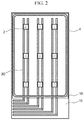
- FIG. 2 is a top view of the multilayer glass 1 .
- FIG. 3 is a side cross-sectional view of an LED 2 , depicting its structure.
- FIG. 4 is a side cross-sectional view of a multilayer glass 1 pertaining to a second embodiment of the present invention, depicting the multilayer glass structure.
- FIG. 5 is a side cross-sectional view of a multilayer glass 1 pertaining to a third embodiment of the present invention, depicting the multilayer glass structure.
- FIG. 6A is a side cross-sectional view depicting a structure example in which conductors 31 and 32 are placed to extend in directions that are orthogonal to each other.
- FIG. 6B is a top view of FIG. 6A .
- FIG. 7 is a top view of a multilayer glass 1 pertaining to a fourth embodiment of the present invention.
- FIG. 8A is a top view of a multilayer glass 1 pertaining to a fifth embodiment of the present invention, depicting the multilayer glass structure.
- FIG. 8B is a front view of FIG. 8A .
- FIG. 9 is a side cross-sectional view of the camera 7 , depicting its structure.
- FIG. 10 is a front view of a multilayer glass 1 pertaining to a sixth embodiment of the present invention, depicting the multilayer glass structure.
- FIG. 11 is a top cross-sectional view of the multilayer glass 1 in the sixth embodiment.
- FIG. 12 is a diagram depicting a utilization example of a multilayer glass 1 pertaining to a seventh embodiment of the present invention.
- FIG. 13 depicts a configuration example in which multilayer glasses 1 c are placed on the front door of a refrigerator.
- FIG. 14 is a cross-sectional view of a multilayer glass 1 c , depicting its structure.
- FIG. 15 is a cross-sectional view of a multilayer glass 1 c , depicting another structure example.
- FIG. 1 is a side cross-sectional view of a multilayer glass 1 pertaining to a first embodiment of the present invention, depicting the multilayer glass structure.
- Two glass plates 10 and 11 are placed to face each other across a gap 5 .
- conductors 30 are formed on the surface of a glass plate 11 and optical elements (e.g., light-emitting diodes (LEDs)) 2 are installed.
- the conductors 30 and the LEDs 2 are electrically connected with each other.
- LEDs light-emitting diodes
- the glass plates 10 and 11 are of planar glass and, for example, those having high transmittance for visible light can be used as them.
- the surface of the inner side (abutting the gap 5 ) of each glass plate is preferably flat from a perspective of convenience for placing conductors 30 thereon, but the inner side may, for example, have a gently curved surface.
- the glass plates 10 and 11 are not necessarily required to be equal in size. Although the type of the glass plates 10 and 11 is not defined specifically, soda-lime glass, white sheet glass, air-cooled hardened glass, etc. may expediently be used.
- FIG. 2 is a top view of the multilayer glass 1 (viewed from above the glass plate 10 ).
- the surface area of the glass plate 11 is larger than the surface area of the glass plate 10 .
- portions along the inner perimeter of the glass plate 10 are sealed with a low-temperature sealing material 4 that works at a low process temperature.
- the gap 5 is sealed in a vacuum or near vacuum state by the low-temperature sealing material 4 .
- the conductors 30 are each formed in two wires connected to an anode and a cathode of an LED 2 . Separate conductors 30 may be provided for each LED 2 or a plurality of LEDs 2 may be connected in series with a single conductor 30 , as depicted in FIG. 2 . If the LEDs 2 are arranged at lattice points, a plurality of pairs of conductors 30 may also be provided.
- the conductors 30 are formed so as to be pulled out. By connecting these pulled out conductors with an external circuit (not depicted), power can be supplied to the LEDs 2 . By making this part having the pulled out conductors non-overlapping with the glass plate 10 , connection with an external circuit and assembly are facilitated. In the case of sandwiching the conductors 30 between the glass plates, as depicted in FIG. 2 , seal thickness in portions where the conductors 30 are sandwiched may be increased to enhance gas barrier performance.
- the LEDs 2 are turned on by applying a voltage to the LEDs 2 from an external circuit (not depicted) via the conductors 30 .
- Light of the LEDs 2 mainly irradiates the outside periphery of the multilayer glass through the glass plates 10 and 11 .
- FIG. 3 is a side cross-sectional view of an LED 2 , depicting its structure.
- An LED element 21 is electrically connected to lead frames 24 and 25 of a package 22 and sealed by sealing resin 23 ; the LED 2 as a whole is thus packaged.
- an LED provided with a lens function can be used.
- a wavelength of light emitted by an LED 2 (visible light, an ultraviolet region, an infrared region, etc.) can be selected according to application and LEDs 2 of different wavelengths may be used concurrently.
- a phosphor which emits light, excited by light of the LED element 21 may be mixed for use in the sealing resin 23 .
- a blue light LED 2 with a yellow light phosphor can create white light.
- a packaged LED 2 since its light emission direction can be controlled, it is, for example, effective in a case where it is desired to emit light in a direction of one side of the multilayer glass 1 .
- the conductors 30 metal wires having a low electrical resistance can be used.
- the conductors 30 are formed in advance on the glass plate.
- ITO indium tin oxide
- IZO indium zinc oxide
- carbon nanotube among others, because the conductors 30 become less apparent.
- Even metal wires can be made nearly transparent by thinning its film thickness.
- FPC Flexible Printed Circuit
- the low-temperature sealing material 4 it is preferable to use a sealing material whose melting point is as low as possible and its softening point is preferably not more than 350° C., and more preferably, not more than 300° C.
- the softening point termed here refers to a second endothermic peak temperature by differential thermal analysis (DTA).
- DTA differential thermal analysis
- vanadic glass glass containing vanadium as a constituent element
- AG 2 O—V 2 O 5 —TeO 2 has a softening point ranging from, approximately, 220° C. to 280° C. and it is preferable as the low-temperature sealing material 4 , because it can seal the gap 5 at the above-mentioned temperature.
- the sealing material for hardened glass in which compression stress is relieved and its hardening performance decreases when its temperature is increased up to 400° C. or above.
- a substance mentioned below in a very low dose to vanadic glass: BaO, WO 3 , Y 2 O 3 , La 2 O 3 , Al 2 O 3 , Fe 2 O 3 , etc.
- ZWP filter low thermal expansion filler
- a metal filler such as Sn or Al
- a way that heats the entire multilayer glass 1 at a temperature from 220° C. to 280° C. or a way that locally heats only in the vicinity of the seal portions may be used.
- the glass may be prevented from being broken by preheating the entire glass to decrease the temperature difference between locally heated portions and other portions. Since the melting point of the low-temperature sealing material 4 is low, even in a case where the sealing process is performed after optical elements 2 are installed within the gap 5 , damage to these members can be reduced. Moreover, even in a case where the conductors 30 are disposed in the vicinity of the seal portions as depicted in FIG. 2 , damage to the conductors 30 can be reduced.
- Vanadic glass has low gas permeability, while having a property of adsorbing gas. Hence, when the gap 5 is put in a vacuum state (or near vacuum state), it is possible to adsorb internal gas, while preventing entering of air from outside, and therefore, the degree of vacuum after sealing can be increased or maintained.
- the gap 5 is a space that is sandwiched between the glass plates 10 and 11 and formed inside the multilayer glass.
- the distance between the glass plates 10 and 11 ranges, for example, approximately, from 0.2 mm to 10 mm.
- the gap 5 is internally vacuum, e.g., at approximately 10 ⁇ circumflex over ( ) ⁇ -3 Pa, from a perspective of adiabaticity.
- argon gas, air, or a desiccant may be packed in the gap 5 .
- the gap 5 In either a case where the gap 5 is made internally vacuum or a case where gas is packed, the gap 5 has a refraction index of 1, whereas optical members such as lenses which are mounted on the optical elements 2 (e.g., LEDs or cameras) are made of glass or resin having a refraction index of 1.4 to 1.6. Hence, the difference between these refraction indexes enables the optical members to function as lenses.
- optical members such as lenses which are mounted on the optical elements 2 (e.g., LEDs or cameras) are made of glass or resin having a refraction index of 1.4 to 1.6.
- the multilayer glass 1 pertaining to this first embodiment uses the low-temperature sealing material 4 (e.g., vanadic glass) in the seal portions, it is possible to decrease processing temperature when joining the glass plates 10 and 11 together and reduce thermal damage to the LEDs 2 and the conductors 30 .
- vanadic glass adsorbs gas, in a case where the gap 5 is made internally vacuum, it is possible to adsorb gas, even if emitted by the LEDs 2 or the like, and maintain the degree of vacuum. By maintaining the degree of vacuum within the gap 5 , it is possible to maintain the heat insulation property of the multilayer glass 1 .
- the low-temperature sealing material 4 serves as isolation between the gap 5 and outside, it is possible to prevent that the optical elements 2 are exposed to halogen gas or sulfidizing gas and corrodes or deteriorates.
- the low-temperature sealing material 4 provides an advantageous effect of preventing some of light emitted by the LEDs from leaking out of the gap 5 unnecessarily.
- a processing temperature (a softening point for a glass sealing material) when fixing the low-temperature sealing material 4 has an effect on a temperature that is applied to the optical elements mounted on the glass plate and is, preferably, lower than a processing temperature when manufacturing the optical elements 2 or a temperature when mounting the optical elements on the glass. This is because, if the gap 5 is sealed at a higher temperature than the processing temperature for the optical elements 2 , the processing heat for the sealing increases the probability of thermal damage to the optical elements 2 .
- the processing temperature for the optical elements 2 termed here, is, for example, a temperature when depositing semiconductor layers.
- a sealing temperature was set to be lower than this temperature. If a temperature when processing the optical elements 2 differs for different processes, the lowest temperature should be selected as a reference and it is preferable to set the sealing temperature lower than the lowest temperature. In addition, in a case where the optical elements 2 include a member made of resin or the like, it is preferable that a temperature of the optical elements 2 , when fixing the low-temperature sealing material 4 , is set to be lower than either the processing temperature for the resin or the temperature when mounting the optical elements 2 , whichever is higher.
- the spacer 6 can be made of a material such as, e.g., glass, ceramics, and resin.
- the shape of the spacer 6 can be selected appropriately. For instance, if a spherical glass bead is used as the spacer 6 , a suitable number of spacers 6 are distributed within the gap 5 before sealing the gap 5 , and then the gap 5 is sealed.
- columnar spacers 6 may be arranged on the glass plate and fixed by applying heat.
- each spacer 6 should be made higher than the height of the LEDs 2 and each spacer 6 should be placed relatively near each LED 2 . If it is sufficient to avoid that glass plates 10 and 11 contact with each other, the height of each spacer 6 may not necessarily be higher than the height of the LEDs.
- Placing spacers 6 within the gap 5 can prevent the glass plates 10 and 11 from bending and contacting with each other, especially when the gap 5 has internally been put in a vacuum state. In other words, it is possible to prevent degradation in the heat insulation property of the multilayer glass 1 .
- FIG. 5 is a side cross-sectional view of a multilayer glass 1 pertaining to a third embodiment of the present invention, depicting the multilayer glass structure. While a pair of conductors 30 is formed on the surface of the glass plate 11 in the first embodiment (e.g., see FIG. 2 ), a single conductor 31 is formed on the surface of the glass plate 10 and a single conductor 32 is formed on the surface of the glass plate 11 in FIG. 5 . If a plurality of LEDs 2 are present, a plurality of pairs of conductors 31 and 32 can be provided correspondingly. The conductor 31 is electrically connected to one end of an LED 2 and the conductor 32 is electrically connected to the other end of the LED 2 .
- the LED 2 fulfills the same role as the spacer 6 and can prevent the glass plates 10 and 11 from bending and contacting with each other when the gap 5 has been made vacuum. If the number of LEDs 2 is small relative to the area of the glass plates 10 and 11 , there is a possibility that plate portions not contacting with the LEDs bend and therefore spacers 6 may be used additionally.
- FIG. 6A is a side cross-sectional view depicting a structure example in which the conductors 31 and 32 are placed to extend in directions that are orthogonal to each other. While the conductors 31 and 32 extend in the same direction in FIG. 5 , they can be made to extend in directions that are orthogonal to each other.
- FIG. 6B is a top view of FIG. 6A .
- a plurality of LEDs are arranged at lattice points.
- Conductors 31 extend in a vertical direction of FIG. 6B and conductors 32 extend in a horizontal direction of FIG. 6B , and they are placed crossing in a lattice form.
- By arranging the conductors 31 and 32 in a lattice form as in FIG. 6B it is possible to selectively cause LEDs 2 arranged in positions where the conductors 31 and 32 cross to emit light. This enables formation of a particular light emission pattern corresponding to, for example, a character or the like.
- each LED 2 since both the top and bottom edges of each LED 2 contact with a conductor, heat that is generated when the LEDs 2 emit light can be dissipated through both the glass plates 10 and 11 .
- This provides an advantageous effect of decreasing the temperature of the LEDs 2 and increasing light emission efficiency.
- a nichrome wire or the like may be placed inside the glass plates to heat them appropriately.
- FIG. 7 is a top view of a multilayer glass 1 pertaining to a fourth embodiment of the present invention.
- the conductors 30 are formed only on the surface of the glass palate 11 , as is the case for the first embodiment. However, the conductors 30 are formed so as to be wider than those in the first embodiment and cover most of the surface of the glass plate 11 .
- the low-temperature sealing material 4 it is preferable to use a sealing material whose melting point is as low as possible and its softening point is preferably not more than 350° C., and more preferably, not more than 300° C.
- the softening point termed here refers to a second endothermic peak temperature by differential thermal analysis (DTA).
- DTA differential thermal analysis
- vanadic glass glass containing vanadium as a constituent element
- AG 2 O—V 2 O 5 —TeO 2 has a softening point ranging from, approximately, 220° C. to 280° C. and it is preferable as the low-temperature sealing material 4 , because it can seal the gap 5 at the above-mentioned temperature.
- the sealing material for hardened glass in which compression stress is relieved and its hardening performance decreases when its temperature is increased up to 400° C. or above.
- a substance mentioned below in a very low dose to vanadic glass: BaO, WO 3 , Y 2 O 3 , La 2 O 3 , Al 2 O 3 , Fe 2 O 3 , etc.
- a low thermal expansion filler such as a ZWP filler
- a metal filler such as Sn or Al
- the conductors 30 are configured as is the case for the first through third embodiments and members to reflect light with a particular wavelength may be placed in portions where the conductors 30 are not formed. Alternatively, a subset of the conductors 30 may be used only to reflect light, without being connected to the LEDs 2 .
- FIG. 8A is a top view of a multilayer glass 1 pertaining to a fifth embodiment of the present invention, depicting the multilayer glass structure.
- LEDs 21 , 22 and a camera 7 are installed in the gap 5 as optical elements.
- the LEDs 21 , 22 and the camera 7 are connected to the conductors 30 respectively.
- a viewer 9 is present in front of the multilayer glass 1 and an object 8 is located in the rear of the multilayer glass 1 as viewed from the viewer 9 side.
- FIG. 8B is a front view of FIG. 8A .
- an LED 21 mainly illuminates the viewer 9 side via a glass plate 11 and an LED 22 mainly illuminates the object 8 side via a glass plate 10 .
- the camera 7 captures an image of the viewer 9 side via the glass plate 11 .
- FIG. 9 is a side cross-sectional view of the camera 7 , depicting its structure.
- a sensor unit 71 is mounted on a substrate 72 and the substrate 72 is electrically connected with an FPC 73 .
- the FPC 73 may be integral with a conductor 30 or may be electrically connected to the conductor 30 separately.
- a lens unit 74 is placed above the sensor unit 71 and a mold 75 supports the sensor and the lens integrally. By shifting the position of the lens unit 74 up and down, a focus function for focusing can be implemented.
- the sensor unit 71 is, for example, an image pickup element such as a CMOS sensor or CCD sensor.
- a camera using a pinhole instead of the lens unit 74 can be used.
- an imaging signal to be transmitted and received by the camera 7 it is preferable to propagate an imaging signal to be transmitted and received by the camera 7 using a wire that has less signal degradation.
- a wire that has less signal degradation.
- fixing the FPC with a conductor 30 mounted thereon onto the surface of a glass plate and connecting it with the camera 7 it is possible to form the conductor 30 that is of a better quality than when the conductor 30 is directly formed on the surface of the glass plate.
- the surface of the glass plate 11 may be provided with concave portions or convex portions and the camera 7 may capture an image across these portions; thereby, the glass plate 11 itself can be allowed to function as a lens.
- the surface of the glass plate 10 or 11 may be provided with concave portions or convex portions and can be allowed to function as a lens to converge and spread light.
- these concave portions or convex portions can be used as members for fitting and positioning the LEDs 21 , 22 , and camera 7 .
- one manner of utilization conceivable is that a computer becomes aware of a viewer 9 coming close to the multilayer glass 1 based on an image captured by the camera 7 and the LEDs 21 and 22 illuminate the object 8 according to instructions of the computer.
- a touch sensor may be placed on the viewer 9 side of the glass plate 11 to enable the viewer 9 to perform manipulation input.
- usage as illustrated with FIGS. 8A and 8B is conceivable.
- FIG. 10 is a front view of a multilayer glass 1 pertaining to a sixth embodiment of the present invention, depicting the multilayer glass structure.
- the multilayer glass 1 is used as a windshield or a rear windshield of an automobile.
- the multilayer glass 1 is provided with a plurality of cameras 7 placed on both the right and left sides and parallax images forward or backward from the automobile can be captured by these cameras. This enables acquisition of information of distance from the automobile to an object whose image is to be captured.
- the multilayer glass 1 is further provided with LEDs 2 that serve for, for example, lighting forward or backward from the car at night and can aid image capturing by the cameras 7 .
- FIG. 11 is a top cross-sectional view of the multilayer glass 1 in this sixth embodiment.
- the multilayer glass 1 is comprised of gently curved glass plates 10 and 11 .
- the gap 5 is filled with any material except for the spaces for mounting optical elements.
- the gap 5 is filled with a low-temperature sealing material 4 .
- the low-temperature sealing material 4 needs to be transparent, it is conceivable that, for example, polyvinyl butyral (PVB) in a film form or epoxy resin is used as the low-temperature sealing material 4 .
- PVB polyvinyl butyral
- a curing temperature in this case is preferably not more than 350° C. and, more preferably, not more than 300° C.
- FIG. 12 is a diagram depicting a utilization example of a multilayer glass 1 pertaining to a seventh embodiment of the present invention.
- An example is illustrated here in which multilayer glasses 1 a and 1 b are placed on inside walls of a refrigerator.
- Multilayer glasses 1 a are placed on a rear wall surface and a multilayer glass 1 b is placed on the surface of a separation shelf which separates the inside space of the refrigerator into upper and lower chambers.
- LEDs 2 with which the multilayer glass 1 b is equipped emit light toward both sides of the multilayer glass and LEDs 2 with which the multilayer glasses 1 a are equipped emit light toward one side of the multilayer glass (toward the inside of the refrigerator).
- Coating or a sheet (not depicted) having a high reflection ratio is placed on the outer side of the multilayer glasses 1 a defining the outside of the refrigerator and reflects light from the inside.
- This configuration illuminates the inside of the refrigerator brightly and enables it to look in the upper and lower chambers across the multilayer glass 1 b ; visibility is improved.
- making the gap 5 vacuum enhances adiabaticity, it is suitable to use the multilayer glasses 1 a , 1 b as inner walls of the refrigerator.
- FIG. 13 depicts a configuration example in which multilayer glasses 1 c are placed on the front door of a refrigerator.
- the inside of the refrigerator can be viewed through the multilayer glasses 1 c .
- the multilayer glasses 1 c can be used with either or both of the multilayer glasses 1 a , 1 b described with FIG. 12 or can be used independently.
- FIG. 14 is a cross-sectional view of a multilayer glass 1 c , depicting its structure.
- the multilayer glass 1 c is provided with a glass plate 12 in addition to the configuration described in the first embodiment.
- a light modulation film 100 is placed between glass plates 11 and 12 .
- LEDs 2 emit light toward the inside of the refrigerator.
- the light modulation film 100 is a film that switches, by applying a predetermined voltage or current, between a state in which the film transmits light without scattering light and a state in which the film blocks out or scatters light.
- a polymer-dispersed liquid crystal panel, electrochromic panel, SPD (Suspended Particle Device) among others can be used.
- the light modulation film 100 turns to the light transmitting state and the inside of the refrigerator is illuminated by the LEDs 2 as necessary. This enables it to view the inside of the refrigerator without opening and closing the front door, and therefore, it is possible to save energy consumption to maintain the temperature inside the refrigerator.
- FIG. 15 is a cross-sectional view of a multilayer glass 1 c , depicting another structure example.
- a half mirror 101 may be formed for use on the surface of the outer side of the glass plate 11 defining the outside of the refrigerator.
- the inside of the refrigerator is hard to view when surroundings of the refrigerator are brighter than the inside of the refrigerator, by lighting the LEDs 2 of any of the multilayer glasses 1 a to 1 c to illuminate the inside of the refrigerator, the inside of the refrigerator becomes brighter than the surroundings and the inside of the refrigerator can be viewed without opening the front door.
- a coefficient of overall heat transmission which indicates the heat insulation performance of the multilayer glasses 1 a to 1 c is preferably smaller than 1 W/m 2 ⁇ K, and more preferably, smaller than 0.5 W/m 2 ⁇ K.
- a multilayer glass having two or more layers of gap 5 may be used.
- FIG. 7 is a top view of a multilayer glass 1 pertaining to a fourth embodiment of the present invention.
- the conductors 30 are formed only on the surface of the glass plate 11 , as is the case for the first embodiment. However, the conductors 30 are formed so as to be wider than those in the first embodiment and cover most of the surface of the glass plate 11 .
- the LEDs 2 just the LED elements can be used, in addition to packaged ones. Also in the foregoing embodiments, although examples are described in which optical elements are placed between the glass plates 10 and 11 , it is also possible to add another glass plate separated by a gap. In this case, because of additional gaps, inter alia, heat insulation performance and noise barrier performance can be improved.
Landscapes
- Chemical & Material Sciences (AREA)
- Engineering & Computer Science (AREA)
- Life Sciences & Earth Sciences (AREA)
- Chemical Kinetics & Catalysis (AREA)
- General Chemical & Material Sciences (AREA)
- Geochemistry & Mineralogy (AREA)
- Materials Engineering (AREA)
- Organic Chemistry (AREA)
- Ceramic Engineering (AREA)
- Multimedia (AREA)
- Signal Processing (AREA)
- Joining Of Glass To Other Materials (AREA)
- Power Engineering (AREA)
- Microelectronics & Electronic Packaging (AREA)
- Led Device Packages (AREA)
- Physics & Mathematics (AREA)
- Condensed Matter Physics & Semiconductors (AREA)
- General Physics & Mathematics (AREA)
- Computer Hardware Design (AREA)
Abstract
Description
- 1: multilayer glass,
- 10: glass plate,
- 11: glass plate,
- 2: optical elements (LEDs),
- 30: conductors,
- 4: low-temperature sealing material,
- 5: gap,
- 6: spacer,
- 7: optical element (camera),
- 8: object,
- 9: viewer,
- 100: light modulation film.
Claims (14)
Applications Claiming Priority (3)
| Application Number | Priority Date | Filing Date | Title |
|---|---|---|---|
| JP2015100929 | 2015-05-18 | ||
| JP2015-100929 | 2015-05-18 | ||
| PCT/JP2016/057994 WO2016185776A1 (en) | 2015-05-18 | 2016-03-14 | Double glass |
Publications (2)
| Publication Number | Publication Date |
|---|---|
| US20180294386A1 US20180294386A1 (en) | 2018-10-11 |
| US10566503B2 true US10566503B2 (en) | 2020-02-18 |
Family
ID=57319869
Family Applications (1)
| Application Number | Title | Priority Date | Filing Date |
|---|---|---|---|
| US15/574,007 Expired - Fee Related US10566503B2 (en) | 2015-05-18 | 2016-03-14 | Multilayer glass |
Country Status (3)
| Country | Link |
|---|---|
| US (1) | US10566503B2 (en) |
| JP (1) | JP6688785B2 (en) |
| WO (1) | WO2016185776A1 (en) |
Families Citing this family (4)
| Publication number | Priority date | Publication date | Assignee | Title |
|---|---|---|---|---|
| US10339647B2 (en) * | 2016-10-06 | 2019-07-02 | Toyota Motor Engineering & Manufacturing North America, Inc. | Methods, systems, and media for qualitative and/or quantitative indentation detection |
| WO2020203008A1 (en) * | 2019-03-29 | 2020-10-08 | パナソニックIpマネジメント株式会社 | Glass panel unit |
| US12234983B2 (en) * | 2022-03-11 | 2025-02-25 | Whirlpool Corporation | Refrigerating appliance lighting system |
| KR102785334B1 (en) * | 2024-10-24 | 2025-03-21 | 전북대학교산학협력단 | Transparent display device with improved daytime visibility |
Citations (16)
| Publication number | Priority date | Publication date | Assignee | Title |
|---|---|---|---|---|
| US5665654A (en) * | 1995-02-10 | 1997-09-09 | Micron Display Technology, Inc. | Method for forming an electrical connection to a semiconductor die using loose lead wire bonding |
| JP2002053349A (en) | 2000-08-09 | 2002-02-19 | Central Glass Co Ltd | Low pressure double glass and method for producing the same |
| JP2006524419A (en) | 2003-04-16 | 2006-10-26 | コーニング インコーポレイテッド | Glass package sealed with frit and manufacturing method thereof |
| US20080211384A1 (en) * | 2007-02-01 | 2008-09-04 | Yuichi Sawai | Field Emission Display and Glass Frit |
| JP2009512977A (en) | 2005-10-21 | 2009-03-26 | サン−ゴバン グラス フランス | Light emitting structure having at least one electroluminescent diode, its manufacture and its application |
| US20090155555A1 (en) | 2007-11-20 | 2009-06-18 | Botelho John W | Frit-containing pastes for producing sintered frit patterns on glass sheets |
| US20100129666A1 (en) | 2008-11-24 | 2010-05-27 | Stephan Lvovich Logunov | Laser assisted frit sealing of high cte glasses and the resulting sealed glass package |
| WO2011001987A1 (en) | 2009-06-30 | 2011-01-06 | 旭硝子株式会社 | Glass member with sealing material layer, electronic device using same, and method for manufacturing the electronic device |
| US8192051B2 (en) * | 2010-11-01 | 2012-06-05 | Quarkstar Llc | Bidirectional LED light sheet |
| US20140061623A1 (en) * | 2012-08-30 | 2014-03-06 | Corning Incorporated | Antimony-free glass, antimony-free frit and a glass package that is hermetically sealed with the frit |
| WO2014061515A1 (en) | 2012-10-18 | 2014-04-24 | 日立化成株式会社 | Electronic component, process for producing same, sealing material paste, and filler particles |
| US9214614B2 (en) * | 2013-07-23 | 2015-12-15 | Grote Industries, Llc | Flexible lighting device having unobtrusive conductive layers |
| US9299899B2 (en) * | 2013-07-23 | 2016-03-29 | Grote Industries, Llc | Flexible lighting device having unobtrusive conductive layers |
| US20160096768A1 (en) * | 2014-10-02 | 2016-04-07 | Yamato Electronic Co., Ltd. | Vanadium-Based Glass Material For Local Heat Sealing, Flat Display Using The Same, And Method For Manufacturing The Display |
| US9837587B2 (en) * | 2013-03-28 | 2017-12-05 | Toshiba Hokuto Electronics Corporation | Light-emitting device with improved flexural resistance and electrical connection between layers, production method therefor, and device using light-emitting device |
| US10032753B2 (en) * | 2014-06-20 | 2018-07-24 | Grote Industries, Llc | Flexible lighting device having both visible and infrared light-emitting diodes |
-
2016
- 2016-03-14 WO PCT/JP2016/057994 patent/WO2016185776A1/en not_active Ceased
- 2016-03-14 JP JP2017519046A patent/JP6688785B2/en not_active Expired - Fee Related
- 2016-03-14 US US15/574,007 patent/US10566503B2/en not_active Expired - Fee Related
Patent Citations (22)
| Publication number | Priority date | Publication date | Assignee | Title |
|---|---|---|---|---|
| US5665654A (en) * | 1995-02-10 | 1997-09-09 | Micron Display Technology, Inc. | Method for forming an electrical connection to a semiconductor die using loose lead wire bonding |
| JP2002053349A (en) | 2000-08-09 | 2002-02-19 | Central Glass Co Ltd | Low pressure double glass and method for producing the same |
| JP2006524419A (en) | 2003-04-16 | 2006-10-26 | コーニング インコーポレイテッド | Glass package sealed with frit and manufacturing method thereof |
| US20070007894A1 (en) | 2003-04-16 | 2007-01-11 | Aitken Bruce G | Glass package that is hermetically sealed with a frit and method of fabrication |
| JP2009512977A (en) | 2005-10-21 | 2009-03-26 | サン−ゴバン グラス フランス | Light emitting structure having at least one electroluminescent diode, its manufacture and its application |
| US20090114928A1 (en) * | 2005-10-21 | 2009-05-07 | Saint- Gobain Glass France | Lighting structure comprising at least one light-emitting diode, method for making same and uses thereof |
| US20080211384A1 (en) * | 2007-02-01 | 2008-09-04 | Yuichi Sawai | Field Emission Display and Glass Frit |
| JP2011502947A (en) | 2007-11-20 | 2011-01-27 | コーニング インコーポレイテッド | Frit-containing paste for producing sintered frit patterns on glass sheets |
| US20090155555A1 (en) | 2007-11-20 | 2009-06-18 | Botelho John W | Frit-containing pastes for producing sintered frit patterns on glass sheets |
| US20100129666A1 (en) | 2008-11-24 | 2010-05-27 | Stephan Lvovich Logunov | Laser assisted frit sealing of high cte glasses and the resulting sealed glass package |
| JP2012509830A (en) | 2008-11-24 | 2012-04-26 | コーニング インコーポレイテッド | Laser-assisted frit sealing of high CTE glass and resulting sealing glass package |
| WO2011001987A1 (en) | 2009-06-30 | 2011-01-06 | 旭硝子株式会社 | Glass member with sealing material layer, electronic device using same, and method for manufacturing the electronic device |
| US20120147538A1 (en) | 2009-06-30 | 2012-06-14 | Asahi Glass Company, Limited | Glass member provided with sealing material layer, electronic device using it and process for producing the electronic device |
| US8192051B2 (en) * | 2010-11-01 | 2012-06-05 | Quarkstar Llc | Bidirectional LED light sheet |
| US20140061623A1 (en) * | 2012-08-30 | 2014-03-06 | Corning Incorporated | Antimony-free glass, antimony-free frit and a glass package that is hermetically sealed with the frit |
| WO2014061515A1 (en) | 2012-10-18 | 2014-04-24 | 日立化成株式会社 | Electronic component, process for producing same, sealing material paste, and filler particles |
| US20150270508A1 (en) | 2012-10-18 | 2015-09-24 | Hitachi Chemical Company, Ltd. | Electronic component, process for producing same, sealing material paste, and filler particles |
| US9837587B2 (en) * | 2013-03-28 | 2017-12-05 | Toshiba Hokuto Electronics Corporation | Light-emitting device with improved flexural resistance and electrical connection between layers, production method therefor, and device using light-emitting device |
| US9214614B2 (en) * | 2013-07-23 | 2015-12-15 | Grote Industries, Llc | Flexible lighting device having unobtrusive conductive layers |
| US9299899B2 (en) * | 2013-07-23 | 2016-03-29 | Grote Industries, Llc | Flexible lighting device having unobtrusive conductive layers |
| US10032753B2 (en) * | 2014-06-20 | 2018-07-24 | Grote Industries, Llc | Flexible lighting device having both visible and infrared light-emitting diodes |
| US20160096768A1 (en) * | 2014-10-02 | 2016-04-07 | Yamato Electronic Co., Ltd. | Vanadium-Based Glass Material For Local Heat Sealing, Flat Display Using The Same, And Method For Manufacturing The Display |
Non-Patent Citations (1)
| Title |
|---|
| International Search Report, PCT/JP2016/057994, Jun. 14, 2016, 2 pgs. |
Also Published As
| Publication number | Publication date |
|---|---|
| US20180294386A1 (en) | 2018-10-11 |
| JPWO2016185776A1 (en) | 2018-03-29 |
| JP6688785B2 (en) | 2020-04-28 |
| WO2016185776A1 (en) | 2016-11-24 |
Similar Documents
| Publication | Publication Date | Title |
|---|---|---|
| KR101345493B1 (en) | Light-emitting device | |
| TWI630449B (en) | Moisture-proof structure and display device | |
| US10566503B2 (en) | Multilayer glass | |
| EP1534049A2 (en) | Lighting unit | |
| US8742526B2 (en) | Photoelectric conversion device | |
| TWI283139B (en) | Planar luminescent device including auxiliary electrode | |
| WO2009131092A1 (en) | Light-emitting device, display device, and color conversion sheet | |
| CN104360475B (en) | A kind of display device and preparation method thereof and control method | |
| KR20140003995A (en) | Organic light emitting display device and method for manufacturing the same | |
| JP2007265968A (en) | Organic EL element panel | |
| JPH06160850A (en) | Liquid crystal display | |
| CN104471305A (en) | Illumination device, display device, and tv reception device | |
| CN104582053A (en) | Light emitting device and electronic device | |
| JP3864851B2 (en) | Planar light emitting device | |
| CN116500831B (en) | Photoelectric functional film, light-transmitting component, preparation method thereof, and vehicle | |
| JP2011108564A (en) | Electrooptical device, method of manufacturing the electrooptical device, and electronic device | |
| JP2012198375A (en) | Electro-optic device | |
| KR100683407B1 (en) | Display device and manufacturing method thereof | |
| KR20160053242A (en) | Display device | |
| JP5356278B2 (en) | Display device | |
| CN1959999B (en) | Flat panel display and manufacturing method thereof | |
| CN115527453B (en) | Display module assembly and tiled display device | |
| CN104765197A (en) | Display substrate, display panel, display device and manufacturing method of display substrate | |
| CN220476239U (en) | display device | |
| KR20220136186A (en) | Semiconductor apparatus, display apparatus, photoelectric conversion apparatus, electronic device, illumination apparatus, moving object, and manufacturing method for semiconductor apparatus |
Legal Events
| Date | Code | Title | Description |
|---|---|---|---|
| AS | Assignment |
Owner name: HITACHI, LTD., JAPAN Free format text: ASSIGNMENT OF ASSIGNORS INTEREST;ASSIGNORS:KANEKO, HIROKI;NAITO, TAKASHI;SEKIGUCHI, YOSHIFUMI;AND OTHERS;REEL/FRAME:044123/0395 Effective date: 20171012 |
|
| FEPP | Fee payment procedure |
Free format text: ENTITY STATUS SET TO UNDISCOUNTED (ORIGINAL EVENT CODE: BIG.); ENTITY STATUS OF PATENT OWNER: LARGE ENTITY |
|
| STPP | Information on status: patent application and granting procedure in general |
Free format text: NON FINAL ACTION MAILED |
|
| STPP | Information on status: patent application and granting procedure in general |
Free format text: NON FINAL ACTION MAILED |
|
| STPP | Information on status: patent application and granting procedure in general |
Free format text: FINAL REJECTION MAILED |
|
| STPP | Information on status: patent application and granting procedure in general |
Free format text: NOTICE OF ALLOWANCE MAILED -- APPLICATION RECEIVED IN OFFICE OF PUBLICATIONS |
|
| STPP | Information on status: patent application and granting procedure in general |
Free format text: PUBLICATIONS -- ISSUE FEE PAYMENT RECEIVED |
|
| STCF | Information on status: patent grant |
Free format text: PATENTED CASE |
|
| FEPP | Fee payment procedure |
Free format text: MAINTENANCE FEE REMINDER MAILED (ORIGINAL EVENT CODE: REM.); ENTITY STATUS OF PATENT OWNER: LARGE ENTITY |
|
| LAPS | Lapse for failure to pay maintenance fees |
Free format text: PATENT EXPIRED FOR FAILURE TO PAY MAINTENANCE FEES (ORIGINAL EVENT CODE: EXP.); ENTITY STATUS OF PATENT OWNER: LARGE ENTITY |
|
| STCH | Information on status: patent discontinuation |
Free format text: PATENT EXPIRED DUE TO NONPAYMENT OF MAINTENANCE FEES UNDER 37 CFR 1.362 |
|
| FP | Lapsed due to failure to pay maintenance fee |
Effective date: 20240218 |