US10565123B2 - Hybrid logical to physical address translation for non-volatile storage devices with integrated compute module - Google Patents
Hybrid logical to physical address translation for non-volatile storage devices with integrated compute module Download PDFInfo
- Publication number
- US10565123B2 US10565123B2 US15/726,313 US201715726313A US10565123B2 US 10565123 B2 US10565123 B2 US 10565123B2 US 201715726313 A US201715726313 A US 201715726313A US 10565123 B2 US10565123 B2 US 10565123B2
- Authority
- US
- United States
- Prior art keywords
- memory
- data
- volatile memory
- compute engine
- logical
- Prior art date
- Legal status (The legal status is an assumption and is not a legal conclusion. Google has not performed a legal analysis and makes no representation as to the accuracy of the status listed.)
- Active
Links
- 238000013519 translation Methods 0.000 title claims description 33
- 230000015654 memory Effects 0.000 claims abstract description 529
- 230000003936 working memory Effects 0.000 claims abstract description 93
- 238000004891 communication Methods 0.000 claims description 31
- 239000007787 solid Substances 0.000 claims description 24
- 238000000034 method Methods 0.000 claims description 22
- 230000004044 response Effects 0.000 claims description 12
- 238000010586 diagram Methods 0.000 description 45
- 238000013507 mapping Methods 0.000 description 30
- 230000008569 process Effects 0.000 description 14
- 238000005516 engineering process Methods 0.000 description 12
- 239000000872 buffer Substances 0.000 description 9
- 239000000758 substrate Substances 0.000 description 9
- 230000006870 function Effects 0.000 description 6
- 238000003491 array Methods 0.000 description 5
- 238000007726 management method Methods 0.000 description 5
- 238000012937 correction Methods 0.000 description 4
- 238000013461 design Methods 0.000 description 4
- 238000001514 detection method Methods 0.000 description 4
- 238000001914 filtration Methods 0.000 description 4
- 230000010354 integration Effects 0.000 description 4
- 238000012545 processing Methods 0.000 description 4
- 230000008859 change Effects 0.000 description 3
- XUIMIQQOPSSXEZ-UHFFFAOYSA-N Silicon Chemical compound [Si] XUIMIQQOPSSXEZ-UHFFFAOYSA-N 0.000 description 2
- 239000008186 active pharmaceutical agent Substances 0.000 description 2
- 230000004931 aggregating effect Effects 0.000 description 2
- 230000002776 aggregation Effects 0.000 description 2
- 238000004220 aggregation Methods 0.000 description 2
- 230000006399 behavior Effects 0.000 description 2
- 230000008901 benefit Effects 0.000 description 2
- 230000006835 compression Effects 0.000 description 2
- 238000007906 compression Methods 0.000 description 2
- 230000006837 decompression Effects 0.000 description 2
- 230000000593 degrading effect Effects 0.000 description 2
- 150000002500 ions Chemical class 0.000 description 2
- 230000005291 magnetic effect Effects 0.000 description 2
- 230000005415 magnetization Effects 0.000 description 2
- 239000000463 material Substances 0.000 description 2
- 238000012986 modification Methods 0.000 description 2
- 230000004048 modification Effects 0.000 description 2
- 230000002085 persistent effect Effects 0.000 description 2
- 239000004065 semiconductor Substances 0.000 description 2
- 229910052710 silicon Inorganic materials 0.000 description 2
- 239000010703 silicon Substances 0.000 description 2
- 239000007784 solid electrolyte Substances 0.000 description 2
- 238000013403 standard screening design Methods 0.000 description 2
- 230000001360 synchronised effect Effects 0.000 description 2
- RYGMFSIKBFXOCR-UHFFFAOYSA-N Copper Chemical compound [Cu] RYGMFSIKBFXOCR-UHFFFAOYSA-N 0.000 description 1
- 229910052774 Proactinium Inorganic materials 0.000 description 1
- 229910017629 Sb2Te3 Inorganic materials 0.000 description 1
- 238000013459 approach Methods 0.000 description 1
- 238000013528 artificial neural network Methods 0.000 description 1
- 230000000903 blocking effect Effects 0.000 description 1
- 238000004422 calculation algorithm Methods 0.000 description 1
- 238000004364 calculation method Methods 0.000 description 1
- 239000003990 capacitor Substances 0.000 description 1
- 239000005387 chalcogenide glass Substances 0.000 description 1
- 229910052804 chromium Inorganic materials 0.000 description 1
- CXOXHMZGEKVPMT-UHFFFAOYSA-N clobazam Chemical compound O=C1CC(=O)N(C)C2=CC=C(Cl)C=C2N1C1=CC=CC=C1 CXOXHMZGEKVPMT-UHFFFAOYSA-N 0.000 description 1
- 229910052802 copper Inorganic materials 0.000 description 1
- 239000010949 copper Substances 0.000 description 1
- 230000008878 coupling Effects 0.000 description 1
- 238000010168 coupling process Methods 0.000 description 1
- 238000005859 coupling reaction Methods 0.000 description 1
- 238000012517 data analytics Methods 0.000 description 1
- 238000013479 data entry Methods 0.000 description 1
- 238000013523 data management Methods 0.000 description 1
- 238000007418 data mining Methods 0.000 description 1
- 238000003066 decision tree Methods 0.000 description 1
- 238000011161 development Methods 0.000 description 1
- 239000004744 fabric Substances 0.000 description 1
- 230000005294 ferromagnetic effect Effects 0.000 description 1
- 238000007667 floating Methods 0.000 description 1
- GNPVGFCGXDBREM-UHFFFAOYSA-N germanium atom Chemical group [Ge] GNPVGFCGXDBREM-UHFFFAOYSA-N 0.000 description 1
- 230000006872 improvement Effects 0.000 description 1
- 230000001939 inductive effect Effects 0.000 description 1
- 229910052751 metal Inorganic materials 0.000 description 1
- 239000002184 metal Substances 0.000 description 1
- 238000001465 metallisation Methods 0.000 description 1
- 239000000203 mixture Substances 0.000 description 1
- 230000006855 networking Effects 0.000 description 1
- 229940044442 onfi Drugs 0.000 description 1
- 230000003287 optical effect Effects 0.000 description 1
- 230000008520 organization Effects 0.000 description 1
- 230000009467 reduction Effects 0.000 description 1
- 230000002441 reversible effect Effects 0.000 description 1
- 229910052709 silver Inorganic materials 0.000 description 1
- 239000004332 silver Substances 0.000 description 1
- 238000000638 solvent extraction Methods 0.000 description 1
- 238000012360 testing method Methods 0.000 description 1
- 239000010409 thin film Substances 0.000 description 1
- 238000012546 transfer Methods 0.000 description 1
- WFKWXMTUELFFGS-UHFFFAOYSA-N tungsten Chemical compound [W] WFKWXMTUELFFGS-UHFFFAOYSA-N 0.000 description 1
- 229910052721 tungsten Inorganic materials 0.000 description 1
- 239000010937 tungsten Substances 0.000 description 1
Images


Classifications
-
- G—PHYSICS
- G06—COMPUTING; CALCULATING OR COUNTING
- G06F—ELECTRIC DIGITAL DATA PROCESSING
- G06F12/00—Accessing, addressing or allocating within memory systems or architectures
- G06F12/02—Addressing or allocation; Relocation
- G06F12/08—Addressing or allocation; Relocation in hierarchically structured memory systems, e.g. virtual memory systems
- G06F12/10—Address translation
- G06F12/1009—Address translation using page tables, e.g. page table structures
-
- G—PHYSICS
- G06—COMPUTING; CALCULATING OR COUNTING
- G06F—ELECTRIC DIGITAL DATA PROCESSING
- G06F12/00—Accessing, addressing or allocating within memory systems or architectures
- G06F12/02—Addressing or allocation; Relocation
- G06F12/0223—User address space allocation, e.g. contiguous or non contiguous base addressing
- G06F12/023—Free address space management
- G06F12/0238—Memory management in non-volatile memory, e.g. resistive RAM or ferroelectric memory
- G06F12/0246—Memory management in non-volatile memory, e.g. resistive RAM or ferroelectric memory in block erasable memory, e.g. flash memory
-
- G—PHYSICS
- G06—COMPUTING; CALCULATING OR COUNTING
- G06F—ELECTRIC DIGITAL DATA PROCESSING
- G06F2212/00—Indexing scheme relating to accessing, addressing or allocation within memory systems or architectures
- G06F2212/10—Providing a specific technical effect
- G06F2212/1008—Correctness of operation, e.g. memory ordering
-
- G—PHYSICS
- G06—COMPUTING; CALCULATING OR COUNTING
- G06F—ELECTRIC DIGITAL DATA PROCESSING
- G06F2212/00—Indexing scheme relating to accessing, addressing or allocation within memory systems or architectures
- G06F2212/10—Providing a specific technical effect
- G06F2212/1016—Performance improvement
- G06F2212/1024—Latency reduction
-
- G—PHYSICS
- G06—COMPUTING; CALCULATING OR COUNTING
- G06F—ELECTRIC DIGITAL DATA PROCESSING
- G06F2212/00—Indexing scheme relating to accessing, addressing or allocation within memory systems or architectures
- G06F2212/65—Details of virtual memory and virtual address translation
- G06F2212/657—Virtual address space management
-
- G—PHYSICS
- G06—COMPUTING; CALCULATING OR COUNTING
- G06F—ELECTRIC DIGITAL DATA PROCESSING
- G06F2212/00—Indexing scheme relating to accessing, addressing or allocation within memory systems or architectures
- G06F2212/72—Details relating to flash memory management
- G06F2212/7201—Logical to physical mapping or translation of blocks or pages
Definitions
- Non-volatile semiconductor memory is used in solid state drives (SSD).
- SSD solid state drives
- large scale e.g. petabyte
- FIG. 1 is a block diagram of one embodiment of a solid state drive that comprises a Controller, non-volatile memory for storing data and a compute engine near the location of the data that can be used to perform common data manipulation operations.
- FIG. 2 is a block diagram of one embodiment of a solid state drive that comprises a Controller, non-volatile memory for storing data and a compute engine near the location of the data that can be used to perform common data manipulation operations.
- FIG. 3 is a block diagram of one embodiment of a Front End Processor Circuit with a compute engine.
- the Front End Processor Circuit is part of a Controller.
- FIG. 4 is a block diagram of one embodiment of a Back End Processor Circuit.
- the Back End Processor Circuit is part of a Controller.
- FIG. 5 is a block diagram of one embodiment of a memory package.
- FIG. 6 is a block diagram of one embodiment of a memory die.
- FIG. 7 is a block diagram of one embodiment of a solid state drive that comprises a Controller, non-volatile memory for storing data and a compute engine near the location of the data that can be used to perform common data manipulation operations.
- FIG. 8 is a block diagram of one embodiment of a solid state drive that comprises a Controller, non-volatile memory for storing data and a compute engine near the location of the data that can be used to perform common data manipulation operations.
- FIG. 9 is a block diagram of one embodiment of a Front End Processor Circuit without a compute engine.
- the Front End Processor Circuit is part of a Controller.
- FIG. 10 is a block diagram of one embodiment of a solid state drive that comprises a Controller, non-volatile memory for storing data and a compute engine near the location of the data that can be used to perform common data manipulation operations.
- FIG. 11 is a block diagram of one embodiment of a Back End Processor Circuit with a compute engine.
- the Back End Processor Circuit is part of a Controller.
- FIG. 12 is a block diagram of one embodiment of a solid state drive that comprises a Controller, non-volatile memory for storing data and a compute engine near the location of the data that can be used to perform common data manipulation operations.
- FIG. 13 is a block diagram of one embodiment of a solid state drive that comprises a Controller, non-volatile memory for storing data and a compute engine near the location of the data that can be used to perform common data manipulation operations.
- FIG. 13A is a block diagram of one embodiment of a solid state drive that comprises a Controller, non-volatile memory for storing data and a compute engine near the location of the data that can be used to perform common data manipulation operations.
- FIG. 14 is a block diagram of one embodiment of a memory package with a compute engine.
- FIG. 15 is a block diagram of one embodiment of a solid state drive that comprises a Controller, non-volatile memory for storing data and a compute engine near the location of the data that can be used to perform common data manipulation operations.
- FIG. 16 is a block diagram of one embodiment of a memory die with a compute engine.
- FIG. 17 is a block diagram of one embodiment of a solid state drive that comprises a Controller, non-volatile memory for storing data and a compute engine near the location of the data that can be used to perform common data manipulation operations.
- FIG. 18 is a block diagram of one embodiment of a memory die with circuitry under the memory array.
- FIG. 19 is a block diagram of one embodiment of a memory die with circuitry under the memory array.
- FIG. 20 depicts a portion of a database.
- FIG. 21 is a block diagram of a block of non-volatile memory.
- FIG. 22 is a block diagram illustrating an implementation of a solid state drive (or other memory system) that comprises a Controller, non-volatile memory for storing data and a compute engine near the location of the data that can be used to perform common data manipulation operations, in accordance with some embodiments.
- the system of FIG. 22 reduces the size in memory of logical address to physical address tables by having separate tables for random and sequential workload to thereby provide more memory resources to the compute engine.
- FIG. 23 is a flow chart describing one embodiment of a process for reducing the size in memory of logical address to physical address tables by having separate tables for random and sequential workload to thereby provide more memory resources to the compute engine inside the memory system (e.g. behind the host interface).
- FIG. 24 is a flow chart describing one embodiment of a process performed by a host.
- FIG. 25 is a flow chart describing one embodiment of a process for operating a memory system using separate logical address to physical address tables for random and sequential workload.
- FIG. 26 depicts fine-grained (page based) mapping that has sixteen different map entries (16 physical pages or 2 blocks in total, s sub-blocks/block, 4 pages/sub-block).
- FIG. 27 depicts coarse-grained mapping (sub-block based) that has four different map entries.
- FIG. 28 depicts coarse-grained mapping (erase block based) that has two different map entries.
- SSD solid state drive
- a solid state drive (“SSD”) or other memory system, is proposed that can accelerate performance of big data applications using a hardware accelerator based approach that involves integrating compute engines inside the SSD (or other memory system) to perform common data manipulation operations such as scan, filter, aggregate, and join (and other operations).
- APIs Application Programming Interfaces
- a compute engine is a hardware circuit that can be one or more of the following:
- Hardware accelerator for data access and manipulation operations such as filtering, aggregation, compression/decompression, sorting, grouping, and joining tabular or other forms of data;
- General purpose CPU core such as ARM/ARC/Intel Atom; and/or
- Reconfigurable hardware circuitry such as FPGAs.
- a compute engine (which is separate from a controller) manipulates the contents of the data. For example, it can search a stream of data looking for a specific key (a set of bytes) or can sort the data in some order as specified by the host.
- the concept of compute engines includes but is not limited to compression/decompression engines sometimes available in SSDs.
- Typical memory systems include a controller, non-volatile storage connected to the controller, and local high speed volatile memory (e.g., DRAM) connected to and local to the controller.
- the controller can use the local high speed volatile memory (also referred to as local memory or working memory) as a read buffer, as a write buffer, as a scratch pad and to store logical address to physical address translation tables (“L2P tables”).
- L2P tables logical address to physical address translation tables
- the non-volatile storage is addressed internally to the memory system using physical addresses associated with the one or more memory die.
- the host system will use logical addresses to address the various memory locations. This enables the host to assign data to consecutive logical addresses, while the memory system is free to store the data as it wishes among the locations of the one or more memory die.
- the controller typically performs address translation between the logical addresses used by the host and the physical addresses used by the memory die.
- One example implementation is to maintain tables (i.e. the L2P tables mentioned above) that identify the current translation between logical addresses (such as logical block addresses, known as LBA's) and physical addresses (such as physical block addresses, known as PBA's).
- An entry in the L2P table may include an identification of a logical address and corresponding physical address.
- logical address to physical address tables include the word “tables” they need not literally be tables. Rather, the logical address to physical address tables (or L2P tables) can be any type of data structure.
- the memory space of a memory system is so large that the local memory cannot hold all of the L2P tables.
- the entire set of L2P tables are stored in the non-volatile storage and a subset of the L2P tables are cached (L2P cache) in the local memory.
- L2P cache may utilize up to 95% of the local memory. Using such a large portion of the local memory is not a problem during normal operation of the memory system (e.g., during programming, erasing and reading).
- a non-volatile storage system that maintains reduced size logical address to physical address tables in volatile working memory by maintaining coarse logical address to physical address tables in the working memory for use with storing sequentially accessed data and storing fine logical address to physical address tables in the working memory for use with storing randomly accessed data.
- the memory system (e.g., SSD) is connectable to (or otherwise in communication with) a host.
- the memory system comprises non-volatile memory (e.g., one or more memory packages including one or more memory die), a controller in communication with the non-volatile memory, working memory connected to the controller and configured to store coarse logical address to physical address tables for use with storing sequentially accessed data and fine logical address to physical address tables for use with storing randomly accessed data, and a compute engine positioned within the memory system and in communication with the controller.
- the compute engine is configured to receive compiled code from the host that includes instructions for performing one or more database operations on target data in the non-volatile memory and an indication of whether the target data is sequentially accessed data or randomly accessed data.
- the compute engine performs the one or more database operations based on the code.
- the target data is accessed using the coarse logical address to physical address tables if the indication denotes that the target data is sequentially accessed data and the target data is accessed using the fine logical address to physical address tables if the indication denotes that the target data is randomly accessed data.
- FIGS. 1-19 describe various architectures for memory systems that can implement the technology proposed herein.
- FIG. 1 is a block diagram of one embodiment of SSD 10 that comprises a Controller (SSD Controller) 12 , non-volatile memory packages 14 for storing data, DRAM/ReRAM 16 , and a compute engine 22 near the location of the data that can be used to perform common data manipulation operations.
- FIG. 1 presents a high-level design where the compute engine 22 is integrated within the SSD Controller 12 .
- the compute engine 22 can be, for instance, an ASIC that is part of the SSD Controller system on a chip (“SoC”), or can be integrated (deeper) as a hardware circuit within the SSD controller.
- SoC SSD Controller system on a chip
- FIG. 1 shows the SSD Controller 12 , a SoC, including existing SSD Controller components that comprise FTL engines 32 , ECC engines 34 , and DDR memory controller 36 for controlling DRAM/ReRAM 16 .
- SSD Controller 12 includes the new proposed compute engine 22 that can be used to perform compute operations on data stored in the non-volatile memory of the memory packages. Examples of the compute operations include scanning the data, searching, filtering, sorting, aggregating data, joining data together, as well as other functions on the data.
- FIG. 1 shows the SSD Controller 12 in communication with DRAM/ReRAM 16 and in communication with the set of one or more memory packages 14 .
- the SSD Controller 12 communicates with the memory packages (and/or memory die) using a Toggle Mode interface, which is an asynchronous interface that is able to communicate 32 GB/s.
- a Toggle Mode interface which is an asynchronous interface that is able to communicate 32 GB/s.
- An alternative embodiment could use ONFI interface (Open NAND Flash Interface), which is synchronous and makes use of a clock.
- DRAM/ReRAM 16 is one example of a local memory (e.g., high speed volatile working memory).
- a memory package refers to a structure that contains one or more memory dies (e.g., NAND flash memory dies, ReRAM dies, both NAND and ReRAM, or other non-volatile technologies).
- the term memory package can also refer to managed memory—i.e. a memory package that contains one or more memory dies with an embedded error correction code (“ECC”) engine/controller to correct errors detected during read operations to the memory.
- ECC embedded error correction code
- the memory packages include one or more memory die.
- each memory die will include its own chip enable that can be controlled by SSD Controller 12 .
- multiple memory die may share a chip enable, requiring SSD Controller 12 to use addressing to select between the memory die that share a chip enable.
- the memory die in the memory packages 14 utilize NAND flash memory.
- the memory package can include cross point ReRAM non-volatile memory, which is discussed below.
- FIG. 2 is a block diagram of one embodiment of a solid state drive 100 that comprises a controller 102 , non-volatile memory 104 for storing data, DRAM/ReRAM 106 and a compute engine 114 near the location of the data that can be used to perform common data manipulation operations.
- the embodiment of FIG. 2 includes an SSD controller 102 comprising a Front End Processor Circuit (FEP) 110 and one or more Back End Processor Circuits (BEP) 112 .
- FEP 110 circuit is implemented on an ASIC.
- each BEP circuit 112 is implemented on a separate ASIC.
- the ASICs for each of the BEP circuits 112 and the FEP circuit 110 are implemented on the same semiconductor such that the SSD controller 102 is manufactured as a SoC.
- FEP 110 and BEP 112 both include their own processors.
- FEP 110 and BEP 112 work as a master slave configuration where the FEP 110 is the master and each BEP 112 is a slave.
- FEP circuit 110 implements a flash translation layer, including performing memory management (e.g., garbage collection, wear leveling, etc.), logical to physical address translation, communication with the host, management of DRAM (local volatile memory) and management the overall operation of the SSD (or other non-volatile storage system).
- the BEP circuit 112 manages memory operations in the memory packages/die at the request of FEP circuit 110 .
- the BEP circuit 112 can carry out the read, erase and programming processes.
- the BEP circuit 112 can perform buffer management, set specific voltage levels required by the FEP circuit 110 , perform error correction (ECC), control the Toggle Mode interfaces to the memory packages, etc.
- each BEP circuit 112 is responsible for its own set of memory packages.
- FIG. 2 shows the FEP circuit 110 in communication with each of the BEP circuits 112 .
- the compute engine 114 is designed in as a hardware circuit within FEP 110 .
- the compute engine can access high speed, high-bandwidth memory using the DDR interface to access the DRAM 106 .
- the bandwidth available to the compute engine is limited by the bandwidth that connects the FEP 110 to the BEP 112 .
- DRAM 106 is one example of a local working memory.
- FIG. 3 is a block diagram of one embodiment of an FEP circuit with the compute engine 114 designed into the circuit.
- the FEP circuit of FIG. 3 is one example implementation of FEP circuit 110 of FIG. 2 .
- FIG. 3 shows a PCIe interface 150 to communicate with the host and a host processor 152 in communication with that PCIe interface.
- the host processor 152 can be any type of processes known in the art that is suitable for the implementation.
- the host processor 152 is in communication with a network-on-chip (NOC) 154 .
- NOC network-on-chip
- An NOC is a communication subsystem on an integrated circuit, typically between cores in a SoC. NOC's can span synchronous and asynchronous clock domains or use unclocked asynchronous logic.
- NOC technology applies networking theory and methods to on-chip communications and brings notable improvements over conventional bus and crossbar interconnections.
- NOC improves the scalability of SoCs and the power efficiency of complex SoCs compared to other designs.
- the wires and the links of the NOC are shared by many signals.
- a high level of parallelism is achieved because all links in the NOC can operate simultaneously on different data packets. Therefore, as the complexity of integrated subsystems keep growing, an NOC provides enhanced performance (such as throughput) and scalability in comparison with previous communication architectures (e.g., dedicated point-to-point signal wires, shared buses, or segmented buses with bridges).
- the memory processor 156 Connected to and in communication with NOC 154 is the memory processor 156 , the compute engine 114 , SRAM 160 and a DRAM controller 162 .
- the DRAM controller 162 is used to operate and communicate with the DRAM (e.g., DRAM 106 ).
- SRAM 160 is local RAM memory used by the compute engine 114 or the memory processor 156 .
- the memory processor 156 is used to run the FEP circuit and perform the various memory operations.
- Also in communication with the NOC are two PCIe Interfaces 164 and 166 .
- the SSD controller will include two BEP circuits; therefore there are two PCIe Interfaces 164 / 166 . Each PCIe Interface communicates with one of the BEP circuits.
- the compute engine 114 is positioned (from the perspective of the host) behind the interface 150 to the host (e.g., on the memory system side of the interface to the host) and behind the API exposed by the Controller (e.g., exposed by the FEP circuit).
- FIG. 4 is a block diagram of one embodiment of the BEP circuit.
- the BEP circuit of FIG. 4 is one example implementation of BEP circuit 112 of FIG. 2 .
- FIG. 4 shows a PCIe Interface 200 for communicating with the FEP circuit (e.g., communicating with one of PCIe Interfaces 164 and 166 of FIG. 3 ).
- PCIe Interface 200 is in communication with two NOCs 202 and 204 . In one embodiment the two NOCs can be combined to one large NOC.
- Each NOC ( 202 / 204 ) is connected to SRAM ( 230 / 260 ), a buffer ( 232 / 262 ), processor ( 220 / 250 ), and a data path controller ( 222 / 252 ) via an XOR engine ( 224 / 254 ) and an ECC engine ( 226 / 256 ).
- the ECC engines 226 / 256 are used to perform error correction, as known in the art.
- the XOR engines 224 / 254 are used to XOR the data so that data can be combined and stored in a manner that can be recovered in case there is a programming error.
- the data path controller is connected to an interface module for communicating via four channels with memory packages.
- the top NOC 202 is associated with an interface 228 for four channels for communicating with memory packages and the bottom NOC 204 is associated with an interface 258 for four additional channels for communicating with memory packages.
- Each interface 228 / 258 includes four Toggle Mode interfaces (TM Interface), four buffers and four schedulers. There is one scheduler, buffer and TM Interface for each of the channels.
- the processor can be any standard processor known in the art.
- the data path controllers 222 / 252 can be a processor, FPGA, microprocessor or other type of controller.
- the XOR engines 224 / 254 and ECC engines 226 / 256 are dedicated hardware circuits, known as hardware accelerators. In other embodiments, the XOR engines 224 / 254 and ECC engines 226 / 256 can be implemented in software.
- the scheduler, buffer, and TM Interfaces are hardware circuits.
- FIG. 5 is a block diagram of one embodiment of a memory package.
- the memory package of FIG. 5 is an example implementation of a memory package included in memory packages 14 of FIG. 1 or memory packages 104 of FIG. 2 .
- FIG. 5 shows a plurality of memory die 292 connected to a memory bus (data lines and chip enable lines) 294 .
- the memory bus 294 connects to a Toggle Mode Interface 296 for communicating with the TM Interface of an BEP circuit (see e.g. FIG. 4 ).
- the memory package can include a small controller connected to the memory bus and the TM Interface.
- the memory package can have one or more memory die.
- each memory package includes eight or 16 memory die; however, other numbers of memory die can also be implemented. The technology described herein is not limited to any particular number of memory die.
- FIG. 6 is a functional block diagram of one embodiment of a memory die 300 .
- Memory is one example implementation of memory die 292 of FIG. 5 .
- the components depicted in FIG. 6 are electrical circuits.
- Memory die 300 includes a three dimensional memory structure 326 of memory cells (such as, for example, a 3D array of memory cells), control circuitry 310 , and read/write circuits 328 . In other embodiments, a two dimensional array of memory cells can be used.
- Memory structure 326 is addressable by word lines via a row decoder 324 and by bit lines via a column decoder 332 .
- the read/write circuits 328 include multiple sense blocks 350 including SB 1 , SB 2 , . . .
- SBp sensing circuitry
- I/O input and/or output
- Memory structure 326 may comprise one or more arrays of memory cells including a 3D array.
- the memory structure may comprise a monolithic three dimensional memory structure in which multiple memory levels are formed above (and not in) a single substrate, such as a wafer, with no intervening substrates.
- the memory structure may comprise any type of non-volatile memory that is monolithically formed in one or more physical levels of arrays of memory cells having an active area disposed above a silicon substrate.
- the memory structure may be in a non-volatile memory device having circuitry associated with the operation of the memory cells, whether the associated circuitry is above or within the substrate.
- Control circuitry 310 cooperates with the read/write circuits 328 to perform memory operations (e.g., erase, program, read, and others) on memory structure 326 , and includes a state machine 312 , an on-chip address decoder 314 , a power control module 316 and a temperature detection circuit 318 .
- the state machine 312 provides die-level control of memory operations.
- Temperature detection circuit 318 (which is on memory die 300 ) is configured to detect temperature at the memory structure 326 , and can be any suitable temperature detection circuit known in the art.
- state machine 312 is programmable by software. In other embodiments, state machine 312 does not use software and is completely implemented in hardware (e.g., electrical circuits).
- control circuitry 310 includes registers, ROM fuses and other storage devices for storing default values such as base voltages and other parameters.
- the on-chip address decoder 314 provides an address interface between addresses used by a host or controller to the hardware address used by the decoders 324 and 332 .
- Power control module 316 controls the power and voltages supplied to the word lines and bit lines during memory operations. It can include drivers for word line layers (discussed below) in a 3D configuration, select transistors (e.g., SGS and SGD transistors, described below) and source lines. Power control module 316 may include charge pumps for creating voltages.
- the sense blocks include bit line drivers.
- Multiple memory elements in memory structure 326 may be configured so that they are connected in series or so that each element is individually accessible.
- flash memory devices in a NAND configuration typically contain memory elements connected in series.
- a NAND string is an example of a set of series-connected memory cells and select gate transistors that can be used to implement memory structure 326 as a three-dimensional memory structure.
- a NAND flash memory array may be configured so that the array is composed of multiple NAND strings of which a NAND string is composed of multiple memory cells sharing a single bit line and accessed as a group.
- memory elements may be configured so that each element is individually accessible, e.g., a NOR memory array.
- NAND and NOR memory configurations are exemplary, and memory cells may be otherwise configured.
- the memory cells may be arranged in the single memory device in an ordered array, such as in a plurality of rows and/or columns.
- the memory elements may be arrayed in non-regular or non-orthogonal configurations, or in structures not considered arrays.
- a three dimensional memory array is arranged so that memory cells occupy multiple planes or multiple memory device levels, thereby forming a structure in three dimensions (i.e., in the x, y and z directions, where the z direction is substantially perpendicular and the x and y directions are substantially parallel to the major surface of the substrate).
- a three dimensional memory structure may be vertically arranged as a stack of multiple two dimensional memory device levels.
- a three dimensional memory array may be arranged as multiple vertical columns (e.g., columns extending substantially perpendicular to the major surface of the substrate, i.e., in they direction) with each column having multiple memory cells.
- the vertical columns may be arranged in a two dimensional configuration, e.g., in an x-y plane, resulting in a three dimensional arrangement of memory cells, with memory cells on multiple vertically stacked memory planes.
- Other configurations of memory elements in three dimensions can also constitute a three dimensional memory array.
- the memory elements may be coupled together to form vertical NAND strings with charge-trapping material that traverse across multiple horizontal memory device levels.
- One example of a three dimensional NAND memory array that can be used to implement memory structure 126 can be found in U.S. Pat. No. 9,343,156, incorporated herein by reference in its entirety.
- Three dimensional configurations can be envisioned wherein some NAND strings contain memory elements in a single memory level while other strings contain memory elements which span through multiple memory levels.
- Three dimensional memory arrays may also be designed in a NOR configuration and in a ReRAM configuration.
- an example memory system is a three dimensional memory structure that includes vertical NAND strings with charge-trapping material
- 2D and 3D memory structures can also be used with the technology described herein.
- floating gate memories e.g., NAND-type and NOR-type flash memory
- ReRAM memories magnetoresistive memory (e.g., MRAM)
- phase change memory e.g., PCRAM
- ReRAM memory includes reversible resistance-switching elements arranged in cross point arrays accessed by X lines and Y lines (e.g., word lines and bit lines).
- X lines and Y lines e.g., word lines and bit lines.
- Y lines e.g., word lines and bit lines.
- X lines and Y lines e.g., word lines and bit lines.
- three dimensional memory array that can be used to implement memory structure 126 can be found in U.S. Patent Application 2016/0133836, “High Endurance Non-Volatile Storage,” incorporated herein by reference in its entirety.
- the memory cells may include conductive bridge memory elements.
- a conductive bridge memory element may also be referred to as a programmable metallization cell.
- a conductive bridge memory element may be used as a state change element based on the physical relocation of ions within a solid electrolyte.
- a conductive bridge memory element may include two solid metal electrodes, one relatively inert (e.g., tungsten) and the other electrochemically active (e.g., silver or copper), with a thin film of the solid electrolyte between the two electrodes.
- the conductive bridge memory element may have a wide range of programming thresholds over temperature.
- Magnetoresistive memory stores data by magnetic storage elements.
- the elements are formed from two ferromagnetic plates, each of which can hold a magnetization, separated by a thin insulating layer.
- One of the two plates is a permanent magnet set to a particular polarity; the other plate's magnetization can be changed to match that of an external field to store memory.
- This configuration is known as a spin valve and is the simplest structure for an MRAM bit.
- a memory device is built from a grid of such memory cells. In one embodiment for programming, each memory cell lies between a pair of write lines arranged at right angles to each other, parallel to the cell, one above and one below the cell. When current is passed through them, an induced magnetic field is created.
- Phase change memory exploits the unique behavior of chalcogenide glass.
- One embodiment uses a GeTe—Sb2Te3 super lattice to achieve non-thermal phase changes by simply changing the co-ordination state of the Germanium atoms with a laser pulse (or light pulse from another source). Therefore, the doses of programming are laser pulses.
- the memory cells can be inhibited by blocking the memory cells from receiving the light. Note that the use of “pulse” in this document does not require a square pulse, but includes a (continuous or non-continuous) vibration or burst of sound, current, voltage light, or other wave.
- FIG. 7 is a block diagram of one embodiment of a solid state drive 400 that comprises a controller 402 , non-volatile memory packages 404 for storing data, DRAM/ReRAM 406 , and a compute engine 412 near the location for that data that can be used to perform common data manipulation operations.
- Controller 402 includes FEP circuit 410 .
- compute engine 412 is integrated within FEP circuit 410 and the one or more BEP circuits 422 are now incorporated within the memory packages 404 .
- the SSD controller contains only one ASIC, for the FEP circuit. That is, the SSD controller 402 is in communication with the memory packages 404 , where each memory package includes multiple memory die 420 and one or more BEP circuits 422 .
- memory die 420 is depicted in FIG. 6 .
- BEP circuit 422 is depicted in FIG. 4 .
- FEP circuit 410 with an integrated compute engine 412 is depicted in FIG. 3 .
- DRAM/ReRAM 406 is an example of a local memory (e.g., local high speed working volatile memory).
- FIG. 8 is a block diagram of one embodiment of a solid state drive 450 that comprises a controller 460 , non-volatile memory packages 454 for storing data, DRAM/ReRAM 456 , and a compute engine 464 near the location of the data that can be used to perform common data manipulation operations.
- the compute engine 464 is a standalone ASIC (application specific integrated circuit) that is integrated with the SSD controller 460 as a SoC.
- controller 460 includes a FEP circuit 460 in communication with one or more BEP circuits 462 .
- Compute engine 464 is outside of and connected to FEP circuit 462 , connected to the BEP circuit and connected to the high speed DRAM memory with separate interfaces.
- the bandwidth available to the compute engine 464 is lower than or equal to the bandwidth of the embodiment of FIG. 2 . This implementation is preferred when the development of the FEP circuit 462 and the compute engine 464 needs to be kept separate.
- BEP circuit 422 is depicted in FIG. 4 .
- memory packages 454 is depicted in FIG. 5 .
- DRAM/ReRAM 456 is an example of a local memory (e.g., local high speed volatile working memory).
- FIG. 9 is a block diagram of one embodiment of a FEP circuit without a compute engine, that is suitable for the embodiment of FIG. 8 (e.g., FEP circuit 460 ).
- FIG. 9 shows all the components of FIG. 3 , but without the compute engine. That is, FIG. 9 depicts PCIe interface 150 , host processor 152 , NOC 154 , memory processor 156 , SRAM 160 , DRAM controller 162 , and PCIe Interfaces 164 and 166 .
- the SSD controller will include two BEP circuits; therefore there are two PCIe Interfaces. Each PCIe Interface communicates with one of the BEP circuits. In other embodiments, there can be more or less than two BEP circuits; therefore, there can be more or less than two PCIe Interfaces.
- FIG. 10 is a block diagram of one embodiment of a solid state drive 600 that comprises a controller 602 , non-volatile memory packages 604 for storing data, DRAM/ReRAM 606 , and compute engine 616 near the location of the data that can be used to perform common data manipulation operations.
- Controller 602 includes a FEP circuit 612 connected to one or more BEP circuits 614 .
- a compute engine 616 is integrated with an BEP circuit 614 . That is, the compute engine 616 is implemented in the ASIC for the BEP circuit 614 .
- the bandwidth available to the compute engine is now determined by the number of toggle mode channels present in each BEP circuit and the bandwidth of the toggle mode channels.
- the BEP circuit 614 may also contain an optional interface 620 to connect to the DRAM/ReRAM chip.
- a direct interface to the high speed memory provides the compute engine 616 with fast access to the memory to store temporary working data. In the absence of a direct interface, temporary working data is streamed via the interface that connects the BEP circuits to the FEP circuit.
- FEP circuit 612 is depicted in FIG. 9 .
- memory packages 604 is depicted in FIG. 5 .
- DRAM/ReRAM 606 is an example of a local memory (e.g., local high speed volatile working memory).
- FIG. 11 is a block diagram of one embodiment of an BEP circuit that includes a compute engine.
- the embodiment of the BEP circuit of FIG. 11 is appropriate for use in the embodiment of FIG. 10 (e.g., as an BEP circuit 614 ).
- the components of FIG. 11 are the same as the components of FIG. 4 , but further includes a compute engine 702 connected to the top NOC 202 and a second compute engine 704 connected to the bottom NOC 204 .
- one compute engine can connect to both NOCs.
- the two NOCs are connected together and the combined NOC will connect to one, two or multiple compute engines.
- the channels grouped together can include more or less than four channels.
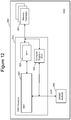
- FIG. 12 is a block diagram of one embodiment of a solid state drive 800 that comprises a controller 802 , non-volatile memory packages 804 for storing data, DRAM/ReRAM 806 and a compute engine 824 near the location of the data that can be used to perform common data manipulation operations.
- Controller 802 includes FEP circuit 820 connected to one or more BEP circuits 822 .
- compute engine 824 is a standalone ASIC that is connected directly to the toggle mode (TM) channels from the BEP circuits.
- the compute engine should optionally include an ECC engine in order to decode and correct data read from the flash memory (or other type of nonvolatile memory in the memory packages) before being processed by the compute engine.
- the compute engine 824 can also be connected to the high speed, high-bandwidth DRAM memory 806 through a standard DDR interface to the DRAM/ReRAM chip and to FEP circuit 820 .
- FEP circuit 820 is depicted in FIG. 9 .
- memory packages 804 is depicted in FIG. 5 .
- BEP circuit 822 is depicted in FIG. 4 .
- DRAM/ReRAM 806 is an example of a local memory (e.g., local high speed volatile memory).
- the embodiments discussed above show various implementations of integrating the compute engine with the controller.
- the compute engine can be integrated with the memory package, referred to as memory package level integration.
- FIG. 13 is a block diagram of one embodiment of a solid state drive 850 that includes memory package level integration, comprising a controller 852 , non-volatile memory packages 854 for storing data, DRAM/ReRAM 856 and a compute engine 862 near the location of the data that can be used to perform common data manipulation operations.
- Controller 852 includes FEP circuit 858 connected to one or more BEP circuits 860 .
- the one or more BEP circuits 860 connect to the non-volatile memory packages 854 .
- FEP circuit 858 is depicted in FIG. 9 .
- One example of BEP circuit 860 is depicted in FIG. 4 .
- DRAM/ReRAM 856 is an example of a local memory (e.g., local high speed volatile working memory).
- the compute engine is integrated with each memory package.
- a memory package which typically includes multiple memory die (e.g., NAND non-volatile memory or other type of non-volatile memory), is now modified to include the compute engine ASIC (also known as a compute engine core) within the memory package.
- the memory package should also include an ECC engine (or at least the decoder portion of the ECC engine) to decode code words read from the memory and to correct the data read from the non-volatile memory die before being processed by the compute engine.
- compute engine 862 includes an ECC engine.
- the compute engine can operate on data that has not been subjected to ECC decoding.
- the memory package can optionally include high-speed memory like DRAM to support the compute engine with access to temporary working data. As the data management operations are within the memory package, the bandwidth available to the compute engine can be much higher than the toggle mode (TM) bandwidth available outside of the memory package.
- FIG. 13A is a block diagram of one embodiment of a solid state drive 880 that includes controller 882 , non-volatile memory packages 884 for storing data, and DRAM/ReRAM 886 .
- Controller 882 includes FEP circuit 888 connected to one or more BEP circuits 890 .
- the one or more BEP circuits 890 connect to the non-volatile memory packages 884 .
- FEP circuit 888 is depicted in FIG. 9 .
- BEP circuit 890 is depicted in FIG. 4 .
- DRAM/ReRAM 886 is an example of a local memory (e.g., local high speed volatile working memory).
- the embodiment depicted in FIG. 13A includes multiple (or distributed) compute engines, such that compute engine 892 is positioned in controller 882 and a set of compute engines (with built-in ECC engine) 894 are positioned in non-volatile memory packages 884 .
- compute engine 892 is a standalone ASIC that is connected directly to the toggle mode (TM) channels from the BEP circuits (the interface between the BEP circuits and the memory packages/die).
- Compute engine 892 can also be connected to the high speed, high-bandwidth DRAM memory 886 through a standard DDR interface to the DRAM/ReRAM chip and to FEP circuit 888 .
- Compute engine 894 is integrated with each memory package.
- the memory package also includes an ECC engine (or at least the decoder portion of the ECC engine) to decode code words read from the memory and to correct the data read from the non-volatile memory die before being processed by the compute engine.
- compute engine 894 includes an ECC engine.
- the compute engine can operate on data that has not been subjected to ECC decoding.
- the memory package can optionally include high-speed memory like DRAM to support the compute engine with access to temporary working data. As some data manipulation operations are within the memory package, the bandwidth available to the compute engine can be much higher than the toggle mode (TM) bandwidth available outside of the memory package.
- the compute engines 892 and 894 will split up the work performed on the data.
- code from the hosts can program the system to perform some operations on compute engine 892 and other operations on compute engine 894 .
- the compute engine 894 could perform error correction coding (ECC) function along with simple application level tests
- the compute engine 892 could be executing a flash translation layer (FTL) optimized for sequential or indexed-sequential workloads, along with more complex filtering, sorting and grouping functions at the application query level.
- ECC error correction coding
- FTL flash translation layer
- FIG. 14 is a block diagram of one embodiment of a memory package that includes a compute engine.
- the embodiment of 14 can be used to implement one of the memory packages 854 in FIG. 13 or memory packages 884 of FIG. 13A .
- the memory package of FIG. 14 includes a plurality of memory die 904 connected to a memory bus 906 (analogous to the memory bus of FIG. 5 ).
- Memory bus 906 is connected to a TM interface 908 for communicating with an BEP circuit.
- FIG. 14 shows a compute engine 910 connected to the memory bus and to an ECC engine 912 .
- the ECC engine 912 is also connected to memory bus 906 .
- Memory read from a memory die can be subjected to ECC decoding (including fixing errors) and then presented to the compute engine 910 to perform any of the compute operations discussed herein.
- FIG. 15 is a block diagram of one embodiment of a solid state drive 950 that comprises a controller 952 , non-volatile memory packages 956 for storing data, DRAM/ReRAM 954 , and a compute engine near the location of that data that can be used to perform common data manipulation operations.
- Controller 952 includes FEP circuit 960 connected to one or more BEP circuits 962 .
- the one or more BEP circuits 962 connect to the non-volatile memory packages 956 .
- FEP circuit 960 is depicted in FIG. 9 .
- One example of BEP circuit 962 is depicted in FIG. 4 .
- DRAM/ReRAM 954 is an example of a local memory (e.g., local high speed volatile working memory).
- each memory package includes multiple memory die and a compute engine 970 integrated within each memory die 972 .
- the compute engine will include an ECC engine to decode (including correcting) data read from the memory die.
- the ECC engine can be part of the compute engine or separate from the compute engine but otherwise included in the memory die.
- the concept of the working memory (or local memory or DRAM discussed above) being connected to the controller includes the working memory being inside the controller.
- a compute engine that is in communication with the controller can be inside or separate from the controller.
- FIG. 16 is a block diagram of one embodiment of a memory die 1000 that includes a compute engine.
- the memory die 1000 is an example implementation of memory die 972 of FIG. 15 .
- the embodiment of FIG. 16 includes the elements of the embodiment of FIG. 6 .
- memory die 1000 includes a three dimensional memory structure 326 of memory cells (such as, for example, a 3D array of memory cells), control circuitry 310 , read/write circuits 328 , row decoder 324 and column decoder 332 .
- Control circuitry 310 includes state machine 312 , on-chip address decoder 314 , a power control module 316 and a temperature detection circuit 318 .
- control circuitry 310 further includes ECC engine 1017 and compute engine 1019 . Data read from the memory structure 326 is decoded using ECC engine 1017 and provided to compute engine 1019 for performing various compute operations, as discussed herein.
- the SSD controller is implemented as a two ASIC solution containing a BEP ASIC and a FEP ASIC
- the design space can be expanded to place the compute engine within any one or more of the ASICs.
- the compute engine can be placed outside of the ASICs.
- the SSD controller can include different architectures, other than the FEP/BEP architecture. Even in the other architectures, the SSD controller can still be configured to include a compute engine inside one of the ASICs or circuits or modules. Additionally, a compute engine can be added to SSDs that are not implemented using ASICs, but implemented using other hardware.
- FIG. 15 includes integrating the compute engine within the memory die (such as a NAND memory die or ReRAM memory die).
- FIG. 17 is a block diagram providing additional details for implementing an embodiment of the system of FIG. 15 .
- FIG. 17 shows a host in communication with a SSD 1100 (implemented on a printed circuit board) that includes a Big NVM controller 1102 and a Small NVM controller 1114 .
- the Big NVM controller 1102 is in communication with DRAM 1104 and memory package 1106 .
- memory package 1106 includes several memory die 1110 , optional DRAM (or MRAM/RRAM/PCM/eDRAM) 1112 , and Small NVM Controller 1114 .
- Each of the memory die 1110 has an on die compute engine (CE).
- the on die compute engine is implemented using CMOS technology on the top surface of a substrate and under the monolithic three-dimensional memory array. Potentially, eDRAM/STT-MRAM/PCM as well as SRAM can be integrated.
- the on die compute engine (CE) can perform some of the data manipulation operations.
- Small NVM Controller 1114 includes a compute engine (CE) that can perform some of the data manipulation operations.
- Small NVM Controller 1114 can communicate with the internal memory dies and external chips (i.e. Big NVM controller and DRAM in FIG. 17 ).
- Optional DRAM 1112 is used for the Small NVM Controller 1114 to store working data sets.
- FIG. 17 shows that each of Big NVM Controller 1102 , DRAM 1104 , memory die 1110 , DRAM 1112 and Small NVM Controller 1114 can be implemented on separate silicon die in three different packages mounted on one printed circuit board.
- FIG. 17 provides a big and small NVM controller architecture.
- the Big NVM Controller 1102 interfaces with the host and DRAM.
- the Small NVM Controller 1114 can be inside any of the memory packages.
- the Small NVM Controller 1114 includes a computational engine with optional DRAM and manages multiple NVM channels.
- a mapping table can be stored in the optional DRAM (or MRAM/PRAM).
- FIG. 18 is a block diagram of one embodiment of a memory die 1200 with circuitry under the memory array.
- FIG. 18 shows a monolithic three-dimensional memory structure 1202 with multiple layers.
- the memory structure 1202 is circuitry 1204 that is implemented on the top surface of the substrate 1206 and under the memory array 1202 .
- the circuitry 1204 is implemented using CMOS technology.
- simple computational logic can be integrated in the CMOS logic under the memory array 1202 potentially with eDRAM/STT-MRAM/PCM as well as SRAM/latches.
- Simple circuitry logic i.e., randomizer, ID generator, PUF, or AES
- simple error management logic i.e., error location map or a simple error avoiding algorithm such as read reference optimizer
- ECC Error Correction Code
- An FPGA could be integrated, supporting multiple configurations with a single system on a chip as an aforementioned compute engine.
- An FPGA can be integrated, supporting multiple configurations within a system on a chip.
- a CPU or parallel computational engine can be integrated as an aforementioned compute engine.
- the compute engine needs to be able to work with encrypted data when AES is bypassed for specific applications.
- the compute engine may need to work with erroneous data when ECC is bypassed for specific applications
- FIG. 19 is a block diagram of one embodiment of a memory die 1300 with circuitry 1304 under the memory array 1302 for using the non-volatile memory die 1300 as a non-volatile-FPGA.
- the memory die 1300 will include a three-dimensional monolithic memory array 1302 .
- CMOS logic 1304 that implements a FPGA to be used as a compute engine (per the discussion above).
- This system will use the memory array 1302 (NAND or other type of non-volatile memory) as configuration storage for the reconfigurable logic 1304 of the FPGA. That is, configuration data stored in memory array 1302 is used to configure the FPGA's.
- the FPGA non-volatile. This will allow for fast boot up compared to conventional FPGAs, which require a reading of configuration data from a discrete nonvolatile memory device to the volatile FPGA cell array.
- the configuration storage the memory array
- the configuration storage can be used as just normal non-volatile storage, saving idle power.
- the complete set of L2P tables are stored in the non-volatile memory (e.g., the Memory Packages), with a subset being cached within local working memory (e.g., see DRAM [or ReRam or SRAM] of FIGS. 1, 2, 7, 8, 10, 12, 13, 13A, 15 , and 17 , or another buffer for the Controller).
- local working memory e.g., see DRAM [or ReRam or SRAM] of FIGS. 1, 2, 7, 8, 10, 12, 13, 13A, 15 , and 17 , or another buffer for the Controller.
- the compute engine discussed above with respect to FIGS. 1-19 will also use the local working memory to stored data while performing its computational operations as described above.
- the use of the local working memory by the compute engine may reduce the space available for the cache storing the L2P tables, thereby, causing a greater “miss” rate for the cache and degrading performance. Limiting the amount of local working memory available to the compute engine will reduce the performance of the compute engine
- L2P tables In the working memory, it is proposed to reduce the amount of space needed to store L2P tables in the working memory without significantly increasing the “miss” rate by maintaining coarse logical address to physical address tables in the working memory for use with sequentially accessed data and maintaining fine logical address to physical address tables in the working memory for use with randomly accessed data.
- Certain embodiments disclosed herein take advantage of special access patterns of database applications (or other applications) to use a lower granularity of L2P tables (e.g., erase block level entry L2P tables) for data with known sequential access patterns. Other intermediate levels of granularity such as sub-erase block or word line can also be used with these known sequential access patterns. Page level entries are continued to be used for data with known random access patterns.
- FIG. 20 depicts a portion of an example database and illustrates an example of randomly accessed data and sequentially accessed data.
- FIG. 20 shows two levels of branch nodes and one level of leaf nodes.
- the branch nodes act as indexes to lower level nodes.
- the leaf nodes can include many data entries (e.g., in this case names).
- the first level of branch nodes includes nodes B, F, H and Sam.
- Node B points to nodes Ba, C and Cr of the second level of branch nodes.
- Node F points to nodes Fe, Kar and Lu of the second level of branch nodes.
- Node N points to nodes Na, Pa and Ph of the second level of branch nodes.
- Node Sam points to nodes Samm, St and V of the second level of branch nodes.
- Branch node Kar points to leaf nodes Krl, Kathy, Ken and Kim.
- Branch node Lu points to leaf nodes Luis, Mark, Mary, Mike and Manny.
- Branch node Na points to leaf nodes Nan, Nancy, Nicky, Nicole and Norm.
- Branch node Pa points to leaf nodes Pablo, Paul, Paula and Peter.
- Branch node Ph points to leaf nodes Phil, Pierre, Rachel, Rajiv and Raoul.
- the branch nodes are accesses randomly and, therefore, are determined to be randomly accessed data (for a random workload).
- the leaf nodes are stored in consecutive addresses (i.e. in alphabetical order) in the non-volatile memory as sequentially accessed data; therefore, they can be written into the non-volatile memory together as such data is serialized using a write buffer between the host and the non-volatile memory for higher performance.
- Log-structured file systems optimized for the non-volatile memory can support aggregation of multiple random write operations into a single sequential write operation. Then, it typically requires sequential reading of the selected leaf blocks for finding a specific node (e.g., finding a specific last name) when it needs to be searched.
- HDFS Hadoop File System
- analytics databases are additional examples that require sequential access to the non-volatile memory.
- the SSD (or other device) workload for the database application can be divided into random and sequential workloads.
- the non-volatile memory can be divided into (at least) two sections.
- a first section (or portion) of memory e.g., a first set of memory cells
- a second section (or portion) of memory e.g., a second set of memory cells
- the first section/portion is physically separate from the second section/portion.
- a first set of memory die for a package or system comprise the first section and a second set of memory die for the package or system comprise the second section.
- the different sections can also be on the same memory die.
- L2P tables for data stored in the second section will include entries for each page of data and are referred to fine L2P tables (or fine logical address to physical address tables).
- L2P tables for data stored in the first section i.e., sequentially accessed data
- L2P tables for data stored in the first section will include entries at the block level and are referred to a coarse L2P tables (or coarse logical address to physical address tables).
- coarse L2P table there is one L2P entry per block, where the block is the unit of erase.
- each L2P entry includes a logical address used by the host and a physical address in the non-volatile memory.
- coarse L2P tables for data stored in the second section will include entries at the word line level or other sub-block level.
- FIG. 21 is a block diagram of an example block of non-volatile memory that includes sixty four word lines (WL 0 -WL 63 ), with each word line having three pages (Page 0 , Page 1 and Page 2 ).
- the example block of FIG. 21 includes 192 pages.
- Other blocks can have more or less than sixty four word lines and more or less than three pages per word line. If the example block of FIG. 21 is used to store random data than the corresponding L2P table would include 192 L2P entries. However, if the example block of FIG.
- FIG. 22 is a block diagram of a block of non-volatile memory system (e.g., a SSD or other device) that reduces the amount of space needed to store L2P tables in the working memory without significantly increasing the “miss” rate by maintaining coarse L2P tables in the working memory for use with sequentially accessed data and maintaining fine L2P tables in the working memory for use with randomly accessed data.
- the block diagram of FIG. 22 while most similar to FIG. 1 , can be used to generalize and applies to any of the embodiments of FIGS. 1-2, 7-8, 10, 12, 13, 13A, 15, and 17-19 .
- FIG. 22 depicts SSD (or other device) 1400 that includes controller 1402 , non-volatile memory 1404 (e.g., Memory Packages) and volatile working memory (e.g., DRAM) 1406 .
- Controller 1402 includes, among other things, a host interface 1420 and a local compute engine 1422 (see more complete discussion above of the compute engine).
- the compute engine can be outside of the controller, including in a memory package (see e.g., the embodiments of FIGS. 13, 13A, 15 and 17-19 ) and/or in a memory die (see e.g., the embodiments of FIGS. 15 and 17-19 ).
- Non-volatile memory 1404 include an area 1430 for storing a complete set of L2P tables, section/portion 1432 configured to store randomly accessed data and a section/portion 1434 configured to store sequentially accessed data. Section 1432 is physically separate from the second section 1434 . In other embodiments, the randomly accessed data and sequentially accessed data can be stored in a common section. In some embodiments, the coarse L2P tables (for sequentially accessed data) are stored in a same area as the fine L2P tables (for randomly accessed data). In other embodiments, the coarse L2P tables (for sequentially accessed data) are stored separately from the fine L2P tables (for randomly accessed data). In one example, the fine L2P tables (for randomly accessed data) are stored in the section 1432 and the coarse L2P tables (for sequentially accessed data) are stored in the section 1434 .
- volatile working memory 1406 includes sequential L2P cache 1440 , random L2P cache 1442 , working data for compute engine 1444 and miscellaneous region 1446 .
- Sequential L2P cache 1440 is a cache that stores a subset of the coarse L2P tables.
- Random L2P cache 1442 is a cache that stores a subset of the fine L2P tables.
- Working data for compute engine 1444 is memory space used by the local compute engine to perform data computations, as discussed above.
- Miscellaneous region 1446 is used by controller 1402 for other purposes.
- Sequential L2P cache 1440 Because the coarse L2P tables stored in Sequential L2P cache 1440 are much smaller than the fine L2P tables, there is more room in volatile working memory 1406 for a bigger working data for compute engine 1444 , which results in higher performance for the local compute engine 1422 .
- compute engine 1422 is configured to use the coarse logical address to physical address tables of the sequential L2P cache 1440 to perform address translation between logical and physical addresses for the leaf nodes for one or more database data structures stored in the portion 1434 of non-volatile memory 1404 and compute engine 1422 is configured to use the fine logical address to physical address tables of random L2P cache 1442 to perform address translation between logical and physical addresses for the branch nodes for one or more database data structures stored in portion 1432 of non-volatile memory 1404 .
- the memory system treats sequentially accessed data different than randomly accessed data.
- the memory system determines whether the data is sequentially accessed data or randomly accessed data.
- the host determines whether the data is sequentially accessed data or randomly accessed data.
- FIG. 22 depicts a host 1460 , in communication with memory system 1400 (via host interface 1420 of controller 1402 ), that determines whether the data is sequentially accessed data or randomly accessed data.
- Host 1460 includes a Just-In-Time Compiler 1462 and a memory interface 1464 .
- Host 1460 determines whether target data being accessed by a set of one or more database operations is randomly accessed data or sequentially accessed data.
- Just-In-Time Compiler 1462 compiles code to perform the set of one or more database operations on a local compute engine 1422 located inside memory system 1400 and embeds in the compiled code an indication of whether the target data is randomly accessed data or sequentially accessed data.
- Memory interface 1464 is used to communicate with host interface 1420 of memory system 1400 , including transmitting the compiled code with the embedded indication to controller 1402 and/or compute engine 1422 (via host interface 1420 ).
- the target data can be accessed by the compute engine performing the address translation or the compute engine requesting (or working with) the controller to perform the address translation.
- the compute engine can perform memory reads (or writes) or the compute engine can work with the controller to perform a memory read (or write).
- FIG. 23 is a flow chart describing one embodiment of a process for reducing the size in memory of L2P tables by having separate tables for random and sequential workload to thereby provide more memory resources to a local compute engine.
- the process of FIG. 23 is performed by memory system 1400 of FIG. 22 (representing any of the embodiments of FIGS. 1-2, 7-8, 10, 12, 13, 15, and 17-19 ).
- the controller (or other entity) maintains reduced size L2P tables in volatile working memory by storing fine L2P tables in the working memory for use with randomly accessed data and coarse L2P tables in the working memory for use with sequentially accessed data.
- the controller performs memory operations using the reduced size L2P tables.
- memory operations e.g., program, erase, read
- coarse L2P tables e.g., program, erase, read
- fine L2P tables e.g., fine L2P tables
- the compute engine inside the controller or outside the controller, or same die as controller or different die than controller
- uses the volatile working memory including extra space due to reduced size L2P tables, to store working data while performing one or more database operations.
- Steps 1502 - 1506 can be performed sequentially or concurrently.
- FIG. 24 is a flow chart describing one embodiment of a process performed by a host when operating a memory system (e.g., such as the memory systems of FIGS. 1-2, 7-8, 10, 12, 13, 15, 17-19 and 22 ) performing the process of FIG. 23 .
- the host determines whether target data being accessed by a set of one or more database operations is randomly accessed data or sequentially accessed data.
- the host e.g., Just-In-Time Compiler 1462 ) compiles code to perform the set of one or more database operations on a compute engine located inside a memory system. The code is compiled for the specific compute engine chosen to perform the task.
- step 1606 the host (e.g., Just-In-Time Compiler 1462 ) embeds in the compiled code an indication of whether the target data is randomly accessed data or sequentially accessed data.
- step 1608 the host (via memory interface 1464 ) transmits the compiled code with the embedded indication to the compute engine (e.g. via host interface 1420 of controller 1402 or any of the other controller architectures described above).
- FIG. 25 is a flow chart describing one embodiment of a process for operating a memory using separate logical address to physical address tables for random and sequential workload.
- the process of FIG. 25 is performed by the memory system (any of the embodiments of FIGS. 1-2, 7-8, 10, 12, 13, 15, 17-19 and 22 ) in response to step 1608 of FIG. 24 .
- the system of FIG. 22 (representing any of the embodiments of FIGS. 1-2, 7-8, 10, 12, 13, 15, and 17-19 ) will perform the process of FIG. 25 on the database of FIG. 20 .
- the memory system receives the compiled code (see step 1608 ) from the host.
- the compiled code is received at host interface 1420 and forwarded to another portion of the controller and/or to the compute engine.
- the compiled code includes instructions for performing one or more database operations on target data in the non-volatile memory.
- the compiled code includes one or more logical addresses for the target data that need to be translated to physical addresses in the non-volatile memory.
- the compiled code also includes an indication of whether the target data is sequentially accessed data or randomly accessed data.
- the indication discussed herein can be a flag or variable that has one value for sequentially accesses data and another value for randomly accessed data.
- the indication can be the logical address used by the host, where a first set of logical addresses are reserved for and indicate sequential data and a second set of logical addresses are reserved for and indicate random data.
- step 1704 the memory system determines whether the target data is sequentially accesses data or randomly accessed data based on reading the indication from the compiled code. This can be performed by the compute engine and/or the controller.
- the memory system classifies the target data as random or sequential and stores randomly accessed data separately from sequentially accessed data. Therefore, based on the data received or addressed the memory system determines whether the job is for random or sequential data. In another embodiment, the memory system can determine whether the job is for randomly accessed data or sequentially accessed data based on the instructions from the host. For example, if the host is requesting sequential reads then the system assumes the job is for sequentially accessed data and if the host is requesting random reads then the system assumes the job is for randomly accessed data. In another embodiment, the memory system can determine whether the job is for randomly accessed data or sequentially accessed data by utilizing a data structure related to the database.
- the instructions from the host are instructions for the local compute engine to perform computations on a set of data. If those instructions are accessing data previously classified as sequentially accessed data then the system assumes the job is for sequentially accessed data and if those are accessing data previously classified as randomly accessed data then the system assumes the job is for randomly accessed data. Alternatively, if those instructions require a scan operation then the system assumes the job is for sequentially accessed data and if those instructions require a seek operation then the systems assumes the job is for randomly accessed data. Similarly, if the instructions cause a sequential writing of data then the operation then the system assumes the job is for sequentially accessed data and if the instructions cause a single write then the operation then the system assumes the job is for randomly accessed data.
- step 1708 the controller and/or compute engine attempts to access the L2P entry for the address received in step 1702 in the appropriate L2P table in the volatile working memory (e.g., DRAM). Since the job is for randomly accessed data, the system attempts to access the L2P entry for a page address in a fine L2P table for random data in the cache of fine L2P tables, such as random L2P cache 1442 . Although all L2P tables are stored in the non-volatile memory, only a subset of L2P tables are stored in the relevant cache.
- the volatile working memory e.g., DRAM
- step 1710 the system fetches the L2P table that includes the page address received in step 1702 from non-volatile memory (e.g., from area 1430 of non-volatile memory 1404 ).
- step 1714 the fetched L2P table is stored in the cache (e.g., in random L2P cache 1742 ).
- step 1716 the L2P entry for the page address received in step 1702 that is in the fetched L2P table is used by the controller and/or compute engine to translate the page address received in step 1702 from a logical address to a physical page address in the non-volatile memory.
- step 1718 one or more operations are performed on the random data associated with the physical page address from step 1716 in response to the instructions received from the host in step 1702 .
- Step 1718 includes the compute engine performing the one or more database operations based on the compiled code, including performing one or more memory operations on randomly accessed target data where the target data is accessed using the fine logical address to physical address tables (see step 1716 ) since the indication denotes that the target data is randomly accessed data. Examples of database operations include scanning the data, searching, filtering, sorting, aggregating data, joining data together, as well as other functions on the data.
- the compute engine will use the local working memory as a scratch pad or for other use.
- step 1710 it is determined that there was a cache hit because the relevant L2P entry was resident in the random L2P cache, then the process proceeds to step 1716 to translate the page address received in step 1702 from the logical address to the physical page address in the non-volatile memory, as described above.
- step 1728 the system attempts to access the L2P entry for a block address (or sub-block or word line or other) in a coarse L2P table for sequential data in the cache of coarse L2P tables, such as sequential L2P cache 3140 . If the L2P entry for the page address received in step 1702 is not in the cache so that there is a cache miss (step 1730 ), then in step 1732 the system fetches the L2P table that includes the block address (or sub-block or word line or other) from non-volatile memory (e.g., from area 1430 of non-volatile memory 1404 ).
- non-volatile memory e.g., from area 1430 of non-volatile memory 1404 .
- step 1734 the fetched L2P table is stored in the cache (e.g., in sequential L2P cache 1440 ).
- step 1736 the L2P entry for the block address received in step 1702 that is in the fetched L2P table is used to translate the block address received in step 1702 from a logical block address to a physical block address in the non-volatile memory. If the address receive in step 1702 is not a block level address, then it is converted into a block address. Note that steps 1716 and 1726 comprise performing address translation for a logical address in the compiled code using coarse L2P tables or fine L2P tables based on the embedded indication.
- step 1738 the compute engine performs the one or more database operations based on the compiled code, including performing one or more memory operations on sequentially accessed target data where the target data was accessed using the coarse logical address to physical address tables (see step 1736 ) since the indication denotes that the target data is sequentially accessed data.
- the compute engine will use the local working memory as a scratch pad or for other use.
- step 1730 it is determined that there was a cache hit because the relevant L2P entry was resident in the sequential L2P cache, then the process proceeds to step 1736 to translate the page address received in step 1702 from the logical address to the physical block address (or sub-block or word line or other) in the non-volatile memory, as described above.
- the non-volatile memory stored a full set of fine L2P tables and a full set of coarse L2P tables.
- the non-volatile memory stores a full set of fine L2P tables and no (or a subset of) coarse L2P tables.
- the controller is configured to create the coarse logical address to physical address tables for the working memory on demand from the fine logical address to physical address mapping tables in the non-volatile memory.
- One embodiment reorganizes the embedded DRAM L2P tables to efficiently support both small block (e.g., 4 KB) writes (e.g., random data operations) and large block writes (100 KB or more) (e.g., sequential data operations). For workloads with a relatively large amount of data requiring large block writes (e.g., sequential data writes), this significantly reduces the amount of DRAM required to hold the L2P cache.
- small block e.g., 4 KB
- large block writes e.g., sequential data operations
- One embodiment assumes a workload with these properties: small block (4 KB or so) reads and writes to a relatively small portion of the overall logical address space; and large block (100 KB or more) writes to the remainder of the logical address space, with both large and small random reads.
- Applications with these properties allow for much more DRAM-efficient mappings for the large block writes: a single mapping entry can represent a much larger region of storage. If the large block writes are performed contiguously to physical storage, the same mapping entry allows small block reads using simple offsets into the large contiguously written block.
- HDFS Hadoop File System
- LSM Log-Structured Merge
- ZFS Zero-Structured file systems
- storage software implementations that perform write serialization for optimized RAID and improved flash performance
- scan-heavy analytics applications include: HDFS (Hadoop File System); Databases using Log-Structured Merge (LSM) trees (including, e.g., Cassandra, LevelDB, and RocksDB); Log-structured file systems, such as ZFS and its derivatives; storage software implementations that perform write serialization for optimized RAID and improved flash performance; and scan-heavy analytics applications.
- LSM Log-Structured Merge
- FIGS. 26-28 depicts L2P tables that can support sequentially accessed data and randomly accessed data, Such tables that supports both small and large block writes can be organized in a variety of ways. These include partitioning for sequentially and randomly written data. FIGS. 26-28 provide more description with examples.
- FIG. 26 depicts an embodiment of fine-grained (page based) mapping in a persistent memory that has sixteen different map entries (16 physical pages or 2 blocks in total, s sub-blocks/block, 4 pages/sub-block).
- the fine-grained (page based) L2P tables of FIG. 26 are for randomly accessed data.
- FIG. 26 shows blocks divided into two sub-blocks. Each sub-block has a set pages. Each page represents data stored in memory cells connected to a common word line, Two types of mapping are depicted: direct mapping and hash mapping. With direct mapping, logical page addresses are mapped to physical page addresses in sequence. With hash mapping, a hash table is used to map a logical page address to any of the physical page addresses, in any order.
- FIG. 27 depicts an embodiment of coarse-grained mapping (sub-block based) that has four different map entries.
- the logical block address can be mapped to physical block address for sequentially accessed data.
- FIG. 27 also teaches to use offsets for the logical block addresses and the physical block addresses to access individual pages so that sequentially accessed data can be accessed randomly. Therefore, the controller and/or the compute engine can be configured to perform a random read of data written as sequentially accessed data using a logical block address and an offset.
- Two types of mapping are depicted: direct mapping and hash mapping. With direct mapping, logical block addresses are mapped to physical block addresses in sequence. With hash mapping, a hash table is used to map a logical block address to any of the physical block addresses, in any order.
- FIG. 28 depicts another embodiment of coarse-grained mapping (erase block based) that has two different map entries.
- the logical block address can be mapped to physical block address for sequentially accessed data.
- FIG. 28 also teaches to use sub-block offsets and page offsets for the logical page addresses and the physical page addresses to access individual pages so that sequentially accessed data can be accessed randomly.
- Two types of mapping are depicted: direct mapping and hash mapping.
- fine grained L2P tables are stored in a persistent memory (i.e. NAND flash, ReRAM, PCM, etc.).
- Logical page addresses can be directly mapped to physical page address, or it can be mapped to certain page addresses through a hash function.
- the fine grained table is reduced into the coarse grained table which is either of sub-block based or erase block based (or other granularity coarser than page level, as discussed above).
- logical page addresses can be randomly read through sub-block offset and page offset values in the logical page address with the coarse grained table that stores sub-block or erase block address translation table.
- coarse-grained mapping based on sub-block or erase block significantly reduce the number of table entries (e.g. 4 for sub-block mapping, 2 for erase-block mapping).
- An extent table contains an ordered set of entries mapping variable sized, contiguous regions of logical addresses to physical locations in storage. This would allow the mappings for an arbitrary mix of various sized writes to be kept in a single table.
- Extent tables of this type can be implemented as a pool of fixed-size records managed as a tree (binary, red-black, B+, etc.) or skip list. Such an organization makes it easy to “page” records between DRAM (the local working memory) and suitable for storage if the entire table cannot fit in DRAM. Other ways to support multiple data sizes in an L2P table should be apparent to someone skilled in the art.
- One embodiment includes an apparatus, comprising a memory system.
- the memory system includes non-volatile memory, a controller in communication with the non-volatile memory, working memory connected to the controller and configured to store a coarse logical address to physical address table for use with storing sequentially accessed data related to database operations and a fine logical address to physical address table for use with storing randomly accessed data related to database operations, and a compute engine positioned within the memory system and in communication with the controller.
- the compute engine is configured to: receive code from a host, the code including instructions for performing one or more database operations on target data in the non-volatile memory and an indication of whether the target data is sequentially accessed data or randomly accessed data, perform the one or more database operations based on the code, and the target data being accessed using the coarse logical address to physical address table in response to the indication denoting that the target data is sequentially accessed data, perform the one or more database operations based on the code, and the target data being accessed using the fine logical address to physical address table in response to the indication denoting that the target data is randomly accessed data.
- the code received from the host is compiled code that includes the indication of whether the target data is sequentially accessed data or randomly accessed data
- the controller includes a host interface
- the compute engine is behind the host interface
- the host interface receives the compiled code from the host and forwards the compiled code to the compute engine
- the compute engine is configured to use the controller to perform address translation between logical and physical addresses for the target data based on the coarse logical address to physical address tables and the fine logical address to physical address tables in the working memory.
- the non-volatile memory includes a memory package that is separate from and connected to the controller and the memory package includes one or more non-volatile memory dies and the compute engine.
- the compute engine is positioned on a first memory die of the one of the non-volatile memory dies; the code received from the host is compiled code that is received by the compute engine on the first memory die; and the compute engine executes the compiled code to access the target data on the first memory die based on the coarse logical address to physical address tables in the working memory for sequentially accessed and the fine logical address to physical address tables in the working memory for data randomly accessed data.
- One embodiment includes a method, comprising: maintaining, in a memory system, reduced size logical to physical (L2P) tables in volatile working memory by maintaining coarse L2P tables in the working memory for use with sequentially accessed data and maintaining fine L2P tables in the working memory for use with randomly accessed data; receiving, by the memory system from a host, compiled code instructing a compute engine within the memory system to perform a set of one or more database operations on target data in the memory system, wherein the compiled code is embedded with an indication of whether the target data is randomly accessed data or sequentially accessed data; using, by the compute engine inside the memory system, the compiled code to perform the set of one or more database operations on the target data using the working memory, including using space in the working memory made available due to reduced size L2P tables, to store working data for the set of one or more database operations; and performing address translation for a logical address in the compiled code using coarse L2P tables or fine L2P tables based on the embedded indication.
- L2P logical to physical
- One embodiment includes a memory system, comprising: non-volatile memory including a first set of memory cells configured to store branch nodes of a database as randomly accessed data and a second set of memory cells configured to store leaf nodes of the database as sequentially accessed data; working memory; and a controller in communication with the non-volatile memory and the working memory.
- the controller includes a host interface.
- the controller is configured to: store a first logical address to physical address table in the working memory for use with storing randomly accessed data in the first set of memory cells and a second logical address to physical address table in the working memory for use with storing sequentially accessed data in the second set of memory cells, the first logical address to physical address table providing address translation at a lower level of granularity than the second logical address to physical address table; receive a request from a host via the host interface, the request including an indication of whether target data of the database to be accessed by the request is sequentially accessed data or randomly accessed data; access the target data from the first set of memory cells using the first logical address to physical address table in response to the request including an indication that the target data is randomly accessed data, and access the target data from the second set of memory cells using the second logical address to physical address table in response to the request including an indication that the target data is sequentially accessed data; and a compute engine that is behind the host interface and is in communication with the controller and the working memory, the compute engine being
- a connection may be a direct connection or an indirect connection (e.g., via one or more others parts).
- the element when an element is referred to as being connected or coupled to another element, the element may be directly connected to the other element or indirectly connected to the other element via intervening elements.
- the element When an element is referred to as being directly connected to another element, then there are no intervening elements between the element and the other element.
- Two devices are “in communication” if they are directly or indirectly connected so that they can communicate electronic signals between them.
- set of objects may refer to a “set” of one or more of the objects.
Abstract
Description
Claims (19)
Priority Applications (2)
| Application Number | Priority Date | Filing Date | Title |
|---|---|---|---|
| US15/726,313 US10565123B2 (en) | 2017-04-10 | 2017-10-05 | Hybrid logical to physical address translation for non-volatile storage devices with integrated compute module |
| PCT/US2018/020152 WO2018190962A1 (en) | 2017-04-10 | 2018-02-28 | Hybrid logical to physical address translation for non-volatile storage devices with integrated compute module |
Applications Claiming Priority (2)
| Application Number | Priority Date | Filing Date | Title |
|---|---|---|---|
| US201762483818P | 2017-04-10 | 2017-04-10 | |
| US15/726,313 US10565123B2 (en) | 2017-04-10 | 2017-10-05 | Hybrid logical to physical address translation for non-volatile storage devices with integrated compute module |
Publications (2)
| Publication Number | Publication Date |
|---|---|
| US20180293174A1 US20180293174A1 (en) | 2018-10-11 |
| US10565123B2 true US10565123B2 (en) | 2020-02-18 |
Family
ID=63711078
Family Applications (1)
| Application Number | Title | Priority Date | Filing Date |
|---|---|---|---|
| US15/726,313 Active US10565123B2 (en) | 2017-04-10 | 2017-10-05 | Hybrid logical to physical address translation for non-volatile storage devices with integrated compute module |
Country Status (2)
| Country | Link |
|---|---|
| US (1) | US10565123B2 (en) |
| WO (1) | WO2018190962A1 (en) |
Cited By (14)
| Publication number | Priority date | Publication date | Assignee | Title |
|---|---|---|---|---|
| US10991444B1 (en) | 2020-05-28 | 2021-04-27 | Western Digital Technologies, Inc. | Tiered read reference calibration |
| US11068342B1 (en) | 2020-06-01 | 2021-07-20 | Western Digital Technologies, Inc. | Redundancy data in integrated memory assembly |
| US11170870B1 (en) | 2020-05-28 | 2021-11-09 | Western Digital Technologies, Inc. | On-chip-copy for integrated memory assembly |
| US11188268B1 (en) | 2020-05-28 | 2021-11-30 | Western Digital Technologies, Inc. | Programmable processor in an integrated memory assembly |
| US11256591B2 (en) | 2020-06-03 | 2022-02-22 | Western Digital Technologies, Inc. | Die memory operation scheduling plan for power control in an integrated memory assembly |
| US11301321B2 (en) | 2020-05-28 | 2022-04-12 | Western Digital Technologies, Inc. | Data shaping for integrated memory assembly |
| US11321167B2 (en) | 2020-05-09 | 2022-05-03 | Western Digital Technologies, Inc. | Adaptive folding for integrated memory assembly |
| US11392327B2 (en) | 2020-09-09 | 2022-07-19 | Western Digital Technologies, Inc. | Local data compaction for integrated memory assembly |
| US11482296B2 (en) | 2020-06-03 | 2022-10-25 | Sandisk Technologies Llc | ECC in integrated memory assembly |
| US11481154B2 (en) | 2021-01-15 | 2022-10-25 | Sandisk Technologies Llc | Non-volatile memory with memory array between circuits |
| US11488682B2 (en) | 2020-06-24 | 2022-11-01 | Sandisk Technologies Llc | Calibration for integrated memory assembly |
| US11650932B2 (en) | 2020-10-25 | 2023-05-16 | Western Digital Technologies, Inc. | Integrated non-volatile memory assembly with address translation |
| US11687252B2 (en) | 2021-10-18 | 2023-06-27 | Western Digital Technologies, Inc. | Non-volatile memory with pre-trained model and inference circuit |
| US11854603B2 (en) | 2021-12-02 | 2023-12-26 | Western Digital Technologies, Inc. | Logical to encoded value table in data storage device |
Families Citing this family (28)
| Publication number | Priority date | Publication date | Assignee | Title |
|---|---|---|---|---|
| US9495288B2 (en) * | 2013-01-22 | 2016-11-15 | Seagate Technology Llc | Variable-size flash translation layer |
| KR102415875B1 (en) * | 2017-07-17 | 2022-07-04 | 에스케이하이닉스 주식회사 | Memory system and operating method of memory system |
| US10289561B2 (en) * | 2017-08-08 | 2019-05-14 | Samsung Electronics Co., Ltd. | Nonvolatile memory devices and methods of controlling the same |
| KR102435890B1 (en) | 2017-08-17 | 2022-08-25 | 삼성전자주식회사 | Address mapping method and operation method of storage device |
| US10503425B2 (en) * | 2017-08-18 | 2019-12-10 | Seagate Technology Llc | Dual granularity dynamic mapping with packetized storage |
| US10977186B2 (en) * | 2017-11-21 | 2021-04-13 | Micron Technology, Inc. | Last written page searching |
| KR20190057887A (en) * | 2017-11-21 | 2019-05-29 | 에스케이하이닉스 주식회사 | Data storage device and operating method thereof |
| KR20190074897A (en) * | 2017-12-20 | 2019-06-28 | 에스케이하이닉스 주식회사 | Memory system and operating method thereof |
| US10346346B1 (en) * | 2017-12-21 | 2019-07-09 | Xilinx, Inc. | Inline ECC function for system-on-chip |
| TWI761440B (en) * | 2018-01-30 | 2022-04-21 | 韓商愛思開海力士有限公司 | memory access method |
| US20190042460A1 (en) * | 2018-02-07 | 2019-02-07 | Intel Corporation | Method and apparatus to accelerate shutdown and startup of a solid-state drive |
| US10754785B2 (en) * | 2018-06-28 | 2020-08-25 | Intel Corporation | Checkpointing for DRAM-less SSD |
| US10871907B2 (en) | 2018-12-31 | 2020-12-22 | Micron Technology, Inc. | Sequential data optimized sub-regions in storage devices |
| KR20200085510A (en) * | 2019-01-07 | 2020-07-15 | 에스케이하이닉스 주식회사 | Data Storage Device, Operation Method Thereof, and Controller Therefor |
| US10901912B2 (en) | 2019-01-28 | 2021-01-26 | Western Digital Technologies, Inc. | Flash translation layer table for unaligned host writes |
| US11010057B2 (en) | 2019-05-29 | 2021-05-18 | Western Digital Technologies, Inc. | Storage system and method for storage system calibration |
| US10997081B2 (en) * | 2019-05-29 | 2021-05-04 | Western Digital Technologies, Inc. | Host and method for storage system calibration |
| US10970211B2 (en) * | 2019-08-02 | 2021-04-06 | EMC IP Holding Company LLC | Techniques for reducing size of log records |
| US11119940B2 (en) * | 2019-08-26 | 2021-09-14 | Micron Technology, Inc. | Sequential-write-based partitions in a logical-to-physical table cache |
| US11487653B2 (en) * | 2019-09-27 | 2022-11-01 | Micron Technology, Inc. | L2P translation techniques in limited RAM systems to increase random write performance using multiple L2P caches |
| US11086786B2 (en) | 2019-12-09 | 2021-08-10 | Westem Digital Technologies, Inc. | Storage system and method for caching a single mapping entry for a random read command |
| US11442631B2 (en) * | 2019-12-26 | 2022-09-13 | Micron Technology, Inc. | Memory operations with consideration for wear leveling |
| US11481317B2 (en) * | 2020-06-26 | 2022-10-25 | Micron Technology, Inc. | Extended memory architecture |
| KR20220060790A (en) * | 2020-11-05 | 2022-05-12 | 에스케이하이닉스 주식회사 | Memory system |
| US11762735B2 (en) * | 2021-10-01 | 2023-09-19 | Western Digital Technologies, Inc. | Interleaved ECC coding for key-value data storage devices |
| US11934264B2 (en) | 2021-11-22 | 2024-03-19 | Western Digital Technologies, Inc. | ECC parity biasing for Key-Value data storage devices |
| US20230350593A1 (en) * | 2022-04-29 | 2023-11-02 | Stmicroelectronics Sa | Method, system, and circuit for deploying file system on embedded memory in programmable computing device |
| US20240086071A1 (en) * | 2022-09-12 | 2024-03-14 | Western Digital Technologies, Inc. | Ssd use of host memory buffer for improved performance |
Citations (117)
| Publication number | Priority date | Publication date | Assignee | Title |
|---|---|---|---|---|
| US6134631A (en) * | 1996-08-19 | 2000-10-17 | Hyundai Electronics America, Inc. | Non-volatile memory with embedded programmable controller |
| US6401185B1 (en) | 1999-05-27 | 2002-06-04 | Oracle Corp. | Method and apparatus for accessing paged objects using a fast division technique |
| US20020116457A1 (en) | 2001-02-22 | 2002-08-22 | John Eshleman | Systems and methods for managing distributed database resources |
| US6446062B1 (en) | 1999-12-23 | 2002-09-03 | Bull Hn Information Systems Inc. | Method and apparatus for improving the performance of a generated code cache search operation through the use of static key values |
| US20020178328A1 (en) | 2001-05-23 | 2002-11-28 | Kiyoshi Honda | Storage subsystem |
| US6549977B1 (en) | 2001-05-23 | 2003-04-15 | 3Ware, Inc. | Use of deferred write completion interrupts to increase the performance of disk operations |
| US20040225831A1 (en) | 2003-05-09 | 2004-11-11 | Tekelec | Methods and systems for preserving dynamic random access memory contents responsive to hung processor condition |
| US6856556B1 (en) | 2003-04-03 | 2005-02-15 | Siliconsystems, Inc. | Storage subsystem with embedded circuit for protecting against anomalies in power signal from host |
| US7055015B2 (en) | 2002-02-25 | 2006-05-30 | Ricoh Company, Ltd. | Information processing apparatus in which processes can reduce overhead of memory access and efficiently share memory |
| US20060143238A1 (en) | 2002-09-10 | 2006-06-29 | Annex Systems Incorporated | Database re-organizing system and database |
| US20070204128A1 (en) | 2003-09-10 | 2007-08-30 | Super Talent Electronics Inc. | Two-Level RAM Lookup Table for Block and Page Allocation and Wear-Leveling in Limited-Write Flash-Memories |
| US20080071785A1 (en) | 2006-08-31 | 2008-03-20 | Microsoft Corporation | Fine-grained access control in a database by preventing information leakage and removing redundancy |
| US20080140918A1 (en) | 2006-12-11 | 2008-06-12 | Pantas Sutardja | Hybrid non-volatile solid state memory system |
| US20080183955A1 (en) | 2007-01-25 | 2008-07-31 | Genesys Logic, Inc. | Flash translation layer apparatus |
| US7424478B2 (en) | 2000-09-01 | 2008-09-09 | Google Inc. | System and method for selecting content for displaying over the internet based upon some user input |
| US7430136B2 (en) | 2004-11-30 | 2008-09-30 | Siliconsystems, Inc. | Purge operations for solid-state storage devices |
| US7447807B1 (en) | 2006-06-30 | 2008-11-04 | Siliconsystems, Inc. | Systems and methods for storing data in segments of a storage subsystem |
| US7509441B1 (en) | 2006-06-30 | 2009-03-24 | Siliconsystems, Inc. | Systems and methods for segmenting and protecting a storage subsystem |
| US20090138654A1 (en) | 2006-12-11 | 2009-05-28 | Pantas Sutardja | Fatigue management system and method for hybrid nonvolatile solid state memory system |
| US7596643B2 (en) | 2007-02-07 | 2009-09-29 | Siliconsystems, Inc. | Storage subsystem with configurable buffer |
| US20090288101A1 (en) | 2008-05-19 | 2009-11-19 | Accenture S.P.A. | Service exception resolution framework |
| US7653778B2 (en) | 2006-05-08 | 2010-01-26 | Siliconsystems, Inc. | Systems and methods for measuring the useful life of solid-state storage devices |
| US7685337B2 (en) | 2007-05-24 | 2010-03-23 | Siliconsystems, Inc. | Solid state storage subsystem for embedded applications |
| US7685338B2 (en) | 2007-05-24 | 2010-03-23 | Siliconsystems, Inc. | Solid state storage subsystem for embedded applications |
| US7685374B2 (en) | 2007-07-26 | 2010-03-23 | Siliconsystems, Inc. | Multi-interface and multi-bus structured solid-state storage subsystem |
| US7733712B1 (en) | 2008-05-20 | 2010-06-08 | Siliconsystems, Inc. | Storage subsystem with embedded circuit for protecting against anomalies in power signal from host |
| US20100174849A1 (en) | 2009-01-07 | 2010-07-08 | Siliconsystems, Inc. | Systems and methods for improving the performance of non-volatile memory operations |
| US7765373B1 (en) | 2006-06-27 | 2010-07-27 | Siliconsystems, Inc. | System for controlling use of a solid-state storage subsystem |
| US7774575B2 (en) | 2004-09-21 | 2010-08-10 | Intel Corporation | Integrated circuit capable of mapping logical block address data across multiple domains |
| US20100250793A1 (en) | 2009-03-24 | 2010-09-30 | Western Digital Technologies, Inc. | Adjusting access of non-volatile semiconductor memory based on access time |
| US20110099323A1 (en) | 2009-10-27 | 2011-04-28 | Western Digital Technologies, Inc. | Non-volatile semiconductor memory segregating sequential, random, and system data to reduce garbage collection for page based mapping |
| US7962792B2 (en) | 2008-02-11 | 2011-06-14 | Siliconsystems, Inc. | Interface for enabling a host computer to retrieve device monitor data from a solid state storage subsystem |
| US20110283048A1 (en) | 2010-05-11 | 2011-11-17 | Seagate Technology Llc | Structured mapping system for a memory device |
| US20110283049A1 (en) | 2010-05-12 | 2011-11-17 | Western Digital Technologies, Inc. | System and method for managing garbage collection in solid-state memory |
| US20110296440A1 (en) | 2010-05-28 | 2011-12-01 | Security First Corp. | Accelerator system for use with secure data storage |
| US8078918B2 (en) | 2008-02-07 | 2011-12-13 | Siliconsystems, Inc. | Solid state storage subsystem that maintains and provides access to data reflective of a failure risk |
| US8090899B1 (en) | 2009-03-04 | 2012-01-03 | Western Digital Technologies, Inc. | Solid state drive power safe wear-leveling |
| US8095851B2 (en) | 2007-09-06 | 2012-01-10 | Siliconsystems, Inc. | Storage subsystem capable of adjusting ECC settings based on monitored conditions |
| US8108692B1 (en) | 2006-06-27 | 2012-01-31 | Siliconsystems, Inc. | Solid-state storage subsystem security solution |
| US8135903B1 (en) | 2009-10-30 | 2012-03-13 | Western Digital Technologies, Inc. | Non-volatile semiconductor memory compressing data to improve performance |
| US8161227B1 (en) | 2006-10-30 | 2012-04-17 | Siliconsystems, Inc. | Storage subsystem capable of programming field-programmable devices of a target computer system |
| US20120179869A1 (en) | 2006-12-06 | 2012-07-12 | Fusion-Io, Inc. | Apparatus, system, and method for data storage using progressive raid |
| US8243525B1 (en) | 2009-09-30 | 2012-08-14 | Western Digital Technologies, Inc. | Refreshing non-volatile semiconductor memory by reading without rewriting |
| US8255661B2 (en) | 2009-11-13 | 2012-08-28 | Western Digital Technologies, Inc. | Data storage system comprising a mapping bridge for aligning host block size with physical block size of a data storage device |
| US8254172B1 (en) | 2009-09-30 | 2012-08-28 | Western Digital Technologies, Inc. | Wear leveling non-volatile semiconductor memory based on erase times and program times |
| US20120221534A1 (en) | 2011-02-28 | 2012-08-30 | International Business Machines Corporation | Database index management |
| US8261012B2 (en) | 2009-10-30 | 2012-09-04 | Western Digital Technologies, Inc. | Non-volatile semiconductor memory comprising power fail circuitry for flushing write data in response to a power fail signal |
| US20120260020A1 (en) | 2011-04-06 | 2012-10-11 | Western Digital Technologies, Inc. | Non-volatile semiconductor memory module enabling out of order host command chunk media access |
| US20120278531A1 (en) | 2011-04-29 | 2012-11-01 | Western Digital Technologies, Inc. | System and method for improved parity determination within a data redundancy scheme in a solid state memory |
| US20120284460A1 (en) | 2011-05-02 | 2012-11-08 | Western Digital Technologies, Inc. | High performance path for command processing |
| US8316176B1 (en) | 2010-02-17 | 2012-11-20 | Western Digital Technologies, Inc. | Non-volatile semiconductor memory segregating sequential data during garbage collection to reduce write amplification |
| US20120324191A1 (en) | 2011-06-14 | 2012-12-20 | Western Digital Technologies, Inc. | System and method for performing data retention that incorporates environmental conditions |
| US8341339B1 (en) | 2010-06-14 | 2012-12-25 | Western Digital Technologies, Inc. | Hybrid drive garbage collecting a non-volatile semiconductor memory by migrating valid data to a disk |
| US8370602B2 (en) | 2008-06-02 | 2013-02-05 | A-Data Technology Co., Ltd. | Method for memory space management |
| US8375151B1 (en) | 2009-02-12 | 2013-02-12 | Siliconsystems, Inc. | Command portal for securely communicating and executing non-standard storage subsystem commands |
| US8392635B2 (en) | 2010-12-22 | 2013-03-05 | Western Digital Technologies, Inc. | Selectively enabling a host transfer interrupt |
| US8397107B1 (en) | 2009-12-11 | 2013-03-12 | Western Digital Technologies, Inc. | Data storage device employing data path protection using both LBA and PBA |
| US8407449B1 (en) | 2010-02-26 | 2013-03-26 | Western Digital Technologies, Inc. | Non-volatile semiconductor memory storing an inverse map for rebuilding a translation table |
| US8423722B1 (en) | 2011-08-26 | 2013-04-16 | Western Digital Technologies, Inc. | System and method for high performance command processing in solid state drives |
| US8443167B1 (en) | 2009-12-16 | 2013-05-14 | Western Digital Technologies, Inc. | Data storage device employing a run-length mapping table and a single address mapping table |
| US8447920B1 (en) | 2010-06-29 | 2013-05-21 | Western Digital Technologies, Inc. | System and method for managing data access in non-volatile memory |
| US20130132638A1 (en) | 2011-11-21 | 2013-05-23 | Western Digital Technologies, Inc. | Disk drive data caching using a multi-tiered memory |
| US8458435B1 (en) | 2010-12-20 | 2013-06-04 | Western Digital Technologies, Inc. | Sequential write thread detection |
| US8503237B1 (en) | 2011-05-18 | 2013-08-06 | Western Digital Technologies, Inc. | System and method for data recovery in a solid state storage device |
| US8521972B1 (en) | 2010-06-30 | 2013-08-27 | Western Digital Technologies, Inc. | System and method for optimizing garbage collection in data storage |
| US8549236B2 (en) | 2006-12-15 | 2013-10-01 | Siliconsystems, Inc. | Storage subsystem with multiple non-volatile memory arrays to protect against data losses |
| US20130290793A1 (en) | 2012-04-25 | 2013-10-31 | Western Digital Technologies, Inc. | Managing unreliable memory in data storage systems |
| US8583835B1 (en) | 2008-08-06 | 2013-11-12 | Siliconsystems, Inc. | Command portal for executing non-standard storage subsystem commands |
| US8601313B1 (en) | 2010-12-13 | 2013-12-03 | Western Digital Technologies, Inc. | System and method for a data reliability scheme in a solid state memory |
| US8601311B2 (en) | 2010-12-14 | 2013-12-03 | Western Digital Technologies, Inc. | System and method for using over-provisioned data capacity to maintain a data redundancy scheme in a solid state memory |
| US8612804B1 (en) | 2010-09-30 | 2013-12-17 | Western Digital Technologies, Inc. | System and method for improving wear-leveling performance in solid-state memory |
| US8612669B1 (en) | 2010-06-28 | 2013-12-17 | Western Digital Technologies, Inc. | System and method for performing data retention in solid-state memory using copy commands and validity and usage data |
| US8615681B2 (en) | 2010-12-14 | 2013-12-24 | Western Digital Technologies, Inc. | System and method for maintaining a data redundancy scheme in a solid state memory in the event of a power loss |
| US20140006898A1 (en) * | 2012-07-02 | 2014-01-02 | Eran Sharon | Flash memory with random partition |
| US8634247B1 (en) | 2012-11-09 | 2014-01-21 | Sandisk Technologies Inc. | NAND flash based content addressable memory |
| US8638602B1 (en) | 2010-09-10 | 2014-01-28 | Western Digital Technologies, Inc. | Background selection of voltage reference values for performing memory read operations |
| US8639872B1 (en) | 2010-08-13 | 2014-01-28 | Western Digital Technologies, Inc. | Hybrid drive comprising write cache spanning non-volatile semiconductor memory and disk |
| US20140059405A1 (en) | 2012-08-21 | 2014-02-27 | Western Digital Technologies, Inc. | Solid-state drive retention monitor using reference blocks |
| US20140082323A1 (en) | 2012-09-14 | 2014-03-20 | Micron Technology, Inc. | Address mapping |
| US8683113B2 (en) | 2011-02-04 | 2014-03-25 | Western Digital Technologies, Inc. | Concurrently searching multiple devices of a non-volatile semiconductor memory |
| US20140101369A1 (en) | 2012-10-05 | 2014-04-10 | Western Digital Technologies, Inc. | Methods, devices and systems for physical-to-logical mapping in solid state drives |
| US8700834B2 (en) | 2011-09-06 | 2014-04-15 | Western Digital Technologies, Inc. | Systems and methods for an enhanced controller architecture in data storage systems |
| US8700950B1 (en) | 2011-02-11 | 2014-04-15 | Western Digital Technologies, Inc. | System and method for data error recovery in a solid state subsystem |
| US8700951B1 (en) | 2011-03-09 | 2014-04-15 | Western Digital Technologies, Inc. | System and method for improving a data redundancy scheme in a solid state subsystem with additional metadata |
| US8707104B1 (en) | 2011-09-06 | 2014-04-22 | Western Digital Technologies, Inc. | Systems and methods for error injection in data storage systems |
| US20140115427A1 (en) | 2012-10-24 | 2014-04-24 | Western Digital Technologies, Inc. | Adaptive error correction codes for data storage systems |
| US8713066B1 (en) | 2010-03-29 | 2014-04-29 | Western Digital Technologies, Inc. | Managing wear leveling and garbage collection operations in a solid-state memory using linked lists |
| US8713357B1 (en) | 2011-09-06 | 2014-04-29 | Western Digital Technologies, Inc. | Systems and methods for detailed error reporting in data storage systems |
| US8725931B1 (en) | 2010-03-26 | 2014-05-13 | Western Digital Technologies, Inc. | System and method for managing the execution of memory commands in a solid-state memory |
| US8724422B1 (en) | 2012-02-29 | 2014-05-13 | Western Digital Technologies, Inc. | System and method for charging back-up charge storage element for data storage device using spindle phase switching elements |
| US20140136753A1 (en) | 2012-11-15 | 2014-05-15 | Western Digital Technologies, Inc. | Methods, data storage devices and systems for fragmented firmware table rebuild in a solid state drive |
| US20140133220A1 (en) | 2012-11-13 | 2014-05-15 | Western Digital Technologies, Inc. | Methods and devices for avoiding lower page corruption in data storage devices |
| US20140149826A1 (en) | 2012-11-29 | 2014-05-29 | Western Digital Technologies, Inc. | Data reliability schemes for data storage systems |
| US20140157078A1 (en) | 2012-12-03 | 2014-06-05 | Western Digital Technologies, Inc. | Methods, solid state drive controllers and data storage devices having a runtime variable raid protection scheme |
| US8751728B1 (en) | 2011-04-29 | 2014-06-10 | Western Digital Technologies, Inc. | Storage system bus transfer optimization |
| US20140181432A1 (en) | 2012-12-26 | 2014-06-26 | Western Digital Technologies, Inc. | Priority-based garbage collection for data storage systems |
| US8769190B1 (en) | 2010-09-15 | 2014-07-01 | Western Digital Technologies, Inc. | System and method for reducing contentions in solid-state memory access |
| US8775720B1 (en) | 2010-08-31 | 2014-07-08 | Western Digital Technologies, Inc. | Hybrid drive balancing execution times for non-volatile semiconductor memory and disk |
| US8773909B2 (en) | 2012-11-09 | 2014-07-08 | Sandisk Technologies Inc. | CAM NAND with or function and full chip search capability |
| US8780632B2 (en) | 2012-11-09 | 2014-07-15 | Sandisk Technologies Inc. | De-duplication techniques using NAND flash based content addressable memory |
| US8780634B2 (en) | 2012-11-09 | 2014-07-15 | Sandisk Technologies Inc. | CAM NAND with OR function and full chip search capability |
| US8782327B1 (en) | 2010-05-11 | 2014-07-15 | Western Digital Technologies, Inc. | System and method for managing execution of internal commands and host commands in a solid-state memory |
| US8788880B1 (en) | 2012-08-22 | 2014-07-22 | Western Digital Technologies, Inc. | Efficient retry mechanism for solid-state memory failures |
| US8788779B1 (en) | 2010-09-17 | 2014-07-22 | Western Digital Technologies, Inc. | Non-volatile storage subsystem with energy-based performance throttling |
| US8788778B1 (en) | 2012-06-04 | 2014-07-22 | Western Digital Technologies, Inc. | Garbage collection based on the inactivity level of stored data |
| US8793429B1 (en) | 2011-06-03 | 2014-07-29 | Western Digital Technologies, Inc. | Solid-state drive with reduced power up time |
| US20140215129A1 (en) | 2013-01-28 | 2014-07-31 | Radian Memory Systems, LLC | Cooperative flash memory control |
| US20140223255A1 (en) | 2012-12-18 | 2014-08-07 | Western Digital Technologies, Inc. | Decoder having early decoding termination detection |
| US8817541B2 (en) | 2012-11-09 | 2014-08-26 | Sandisk Technologies Inc. | Data search using bloom filters and NAND based content addressable memory |
| US8838936B1 (en) | 2013-11-27 | 2014-09-16 | NXGN Data, Inc. | System and method for efficient flash translation layer |
| US8949568B2 (en) | 2011-05-24 | 2015-02-03 | Agency For Science, Technology And Research | Memory storage device, and a related zone-based block management and mapping method |
| US20150106574A1 (en) * | 2013-10-15 | 2015-04-16 | Advanced Micro Devices, Inc. | Performing Processing Operations for Memory Circuits using a Hierarchical Arrangement of Processing Circuits |
| US20150143029A1 (en) * | 2013-11-21 | 2015-05-21 | Sandisk Technologies Inc. | Dynamic logical groups for mapping flash memory |
| US20150143028A1 (en) | 2013-11-18 | 2015-05-21 | SK Hynix Inc. | Data storage apparatus and operating method thereof |
| US9330143B2 (en) | 2013-10-24 | 2016-05-03 | Western Digital Technologies, Inc. | Data storage device supporting accelerated database operations |
| US9348758B2 (en) | 2012-09-24 | 2016-05-24 | Sk Hynix Memory Solutions Inc. | Virtual addressing with multiple lookup tables and RAID stripes |
| US20170177497A1 (en) | 2015-12-21 | 2017-06-22 | Qualcomm Incorporated | Compressed caching of a logical-to-physical address table for nand-type flash memory |
Family Cites Families (2)
| Publication number | Priority date | Publication date | Assignee | Title |
|---|---|---|---|---|
| US9472758B2 (en) | 2014-11-11 | 2016-10-18 | Sandisk Technologies Llc | High endurance non-volatile storage |
| US9343156B1 (en) | 2015-06-25 | 2016-05-17 | Sandisk Technologies Inc. | Balancing programming speeds of memory cells in a 3D stacked memory |
-
2017
- 2017-10-05 US US15/726,313 patent/US10565123B2/en active Active
-
2018
- 2018-02-28 WO PCT/US2018/020152 patent/WO2018190962A1/en active Application Filing
Patent Citations (136)
| Publication number | Priority date | Publication date | Assignee | Title |
|---|---|---|---|---|
| US6134631A (en) * | 1996-08-19 | 2000-10-17 | Hyundai Electronics America, Inc. | Non-volatile memory with embedded programmable controller |
| US6401185B1 (en) | 1999-05-27 | 2002-06-04 | Oracle Corp. | Method and apparatus for accessing paged objects using a fast division technique |
| US6446062B1 (en) | 1999-12-23 | 2002-09-03 | Bull Hn Information Systems Inc. | Method and apparatus for improving the performance of a generated code cache search operation through the use of static key values |
| US7424478B2 (en) | 2000-09-01 | 2008-09-09 | Google Inc. | System and method for selecting content for displaying over the internet based upon some user input |
| US20020116457A1 (en) | 2001-02-22 | 2002-08-22 | John Eshleman | Systems and methods for managing distributed database resources |
| US6549977B1 (en) | 2001-05-23 | 2003-04-15 | 3Ware, Inc. | Use of deferred write completion interrupts to increase the performance of disk operations |
| US20020178328A1 (en) | 2001-05-23 | 2002-11-28 | Kiyoshi Honda | Storage subsystem |
| US7055015B2 (en) | 2002-02-25 | 2006-05-30 | Ricoh Company, Ltd. | Information processing apparatus in which processes can reduce overhead of memory access and efficiently share memory |
| US20060143238A1 (en) | 2002-09-10 | 2006-06-29 | Annex Systems Incorporated | Database re-organizing system and database |
| US6856556B1 (en) | 2003-04-03 | 2005-02-15 | Siliconsystems, Inc. | Storage subsystem with embedded circuit for protecting against anomalies in power signal from host |
| US7126857B2 (en) | 2003-04-03 | 2006-10-24 | Siliconsystems, Inc. | Storage subsystem with embedded circuit for protecting against anomalies in power signal from host |
| US20040225831A1 (en) | 2003-05-09 | 2004-11-11 | Tekelec | Methods and systems for preserving dynamic random access memory contents responsive to hung processor condition |
| US20070204128A1 (en) | 2003-09-10 | 2007-08-30 | Super Talent Electronics Inc. | Two-Level RAM Lookup Table for Block and Page Allocation and Wear-Leveling in Limited-Write Flash-Memories |
| US7774575B2 (en) | 2004-09-21 | 2010-08-10 | Intel Corporation | Integrated circuit capable of mapping logical block address data across multiple domains |
| US7502256B2 (en) | 2004-11-30 | 2009-03-10 | Siliconsystems, Inc. | Systems and methods for reducing unauthorized data recovery from solid-state storage devices |
| US7430136B2 (en) | 2004-11-30 | 2008-09-30 | Siliconsystems, Inc. | Purge operations for solid-state storage devices |
| US7936603B2 (en) | 2004-11-30 | 2011-05-03 | Siliconsystems, Inc. | Purge operations for solid-state storage devices |
| US7898855B2 (en) | 2004-11-30 | 2011-03-01 | Siliconsystems, Inc. | Systems and methods for reducing unauthorized data recovery from solid-state storage devices |
| US8122185B2 (en) | 2006-05-08 | 2012-02-21 | Siliconsystems, Inc. | Systems and methods for measuring the useful life of solid-state storage devices |
| US8312207B2 (en) | 2006-05-08 | 2012-11-13 | Siliconsystems, Inc. | Systems and methods for measuring the useful life of solid-state storage devices |
| US7653778B2 (en) | 2006-05-08 | 2010-01-26 | Siliconsystems, Inc. | Systems and methods for measuring the useful life of solid-state storage devices |
| US8108692B1 (en) | 2006-06-27 | 2012-01-31 | Siliconsystems, Inc. | Solid-state storage subsystem security solution |
| US7765373B1 (en) | 2006-06-27 | 2010-07-27 | Siliconsystems, Inc. | System for controlling use of a solid-state storage subsystem |
| US7912991B1 (en) | 2006-06-30 | 2011-03-22 | Siliconsystems, Inc. | Systems and methods for segmenting and protecting a storage subsystem |
| US8127048B1 (en) | 2006-06-30 | 2012-02-28 | Siliconsystems, Inc. | Systems and methods for segmenting and protecting a storage subsystem |
| US7447807B1 (en) | 2006-06-30 | 2008-11-04 | Siliconsystems, Inc. | Systems and methods for storing data in segments of a storage subsystem |
| US7509441B1 (en) | 2006-06-30 | 2009-03-24 | Siliconsystems, Inc. | Systems and methods for segmenting and protecting a storage subsystem |
| US20080071785A1 (en) | 2006-08-31 | 2008-03-20 | Microsoft Corporation | Fine-grained access control in a database by preventing information leakage and removing redundancy |
| US8161227B1 (en) | 2006-10-30 | 2012-04-17 | Siliconsystems, Inc. | Storage subsystem capable of programming field-programmable devices of a target computer system |
| US20120179869A1 (en) | 2006-12-06 | 2012-07-12 | Fusion-Io, Inc. | Apparatus, system, and method for data storage using progressive raid |
| US20090138654A1 (en) | 2006-12-11 | 2009-05-28 | Pantas Sutardja | Fatigue management system and method for hybrid nonvolatile solid state memory system |
| US20080140918A1 (en) | 2006-12-11 | 2008-06-12 | Pantas Sutardja | Hybrid non-volatile solid state memory system |
| US8549236B2 (en) | 2006-12-15 | 2013-10-01 | Siliconsystems, Inc. | Storage subsystem with multiple non-volatile memory arrays to protect against data losses |
| US20080183955A1 (en) | 2007-01-25 | 2008-07-31 | Genesys Logic, Inc. | Flash translation layer apparatus |
| US7596643B2 (en) | 2007-02-07 | 2009-09-29 | Siliconsystems, Inc. | Storage subsystem with configurable buffer |
| US8151020B2 (en) | 2007-02-07 | 2012-04-03 | Siliconsystems, Inc. | Storage subsystem with configurable buffer |
| US7685337B2 (en) | 2007-05-24 | 2010-03-23 | Siliconsystems, Inc. | Solid state storage subsystem for embedded applications |
| US7685338B2 (en) | 2007-05-24 | 2010-03-23 | Siliconsystems, Inc. | Solid state storage subsystem for embedded applications |
| US8433858B1 (en) | 2007-07-26 | 2013-04-30 | Siliconsystems, Inc. | Multi-interface and multi-bus structured solid-state storage subsystem |
| US8166245B2 (en) | 2007-07-26 | 2012-04-24 | Siliconsystems, Inc. | Multi-interface and multi-bus structured solid-state storage subsystem |
| US7685374B2 (en) | 2007-07-26 | 2010-03-23 | Siliconsystems, Inc. | Multi-interface and multi-bus structured solid-state storage subsystem |
| US8095851B2 (en) | 2007-09-06 | 2012-01-10 | Siliconsystems, Inc. | Storage subsystem capable of adjusting ECC settings based on monitored conditions |
| US8296625B2 (en) | 2007-09-06 | 2012-10-23 | Siliconsystems, Inc. | Storage subsystem capable of adjusting ECC settings based on monitored conditions |
| US8078918B2 (en) | 2008-02-07 | 2011-12-13 | Siliconsystems, Inc. | Solid state storage subsystem that maintains and provides access to data reflective of a failure risk |
| US7962792B2 (en) | 2008-02-11 | 2011-06-14 | Siliconsystems, Inc. | Interface for enabling a host computer to retrieve device monitor data from a solid state storage subsystem |
| US20090288101A1 (en) | 2008-05-19 | 2009-11-19 | Accenture S.P.A. | Service exception resolution framework |
| US7733712B1 (en) | 2008-05-20 | 2010-06-08 | Siliconsystems, Inc. | Storage subsystem with embedded circuit for protecting against anomalies in power signal from host |
| US8370602B2 (en) | 2008-06-02 | 2013-02-05 | A-Data Technology Co., Ltd. | Method for memory space management |
| US8583835B1 (en) | 2008-08-06 | 2013-11-12 | Siliconsystems, Inc. | Command portal for executing non-standard storage subsystem commands |
| US8745277B2 (en) | 2008-08-06 | 2014-06-03 | Siliconsystems, Inc. | Command portal for securely communicating and executing non-standard storage subsystem commands |
| US20130145106A1 (en) | 2008-08-06 | 2013-06-06 | Western Digital Technologies, Inc. | Command portal for securely communicating and executing non-standard storage subsystem commands |
| US20100174849A1 (en) | 2009-01-07 | 2010-07-08 | Siliconsystems, Inc. | Systems and methods for improving the performance of non-volatile memory operations |
| US8375151B1 (en) | 2009-02-12 | 2013-02-12 | Siliconsystems, Inc. | Command portal for securely communicating and executing non-standard storage subsystem commands |
| US8478930B1 (en) | 2009-03-04 | 2013-07-02 | Western Digital Technologies, Inc. | Solid state drive power safe wear-leveling |
| US8090899B1 (en) | 2009-03-04 | 2012-01-03 | Western Digital Technologies, Inc. | Solid state drive power safe wear-leveling |
| US20100250793A1 (en) | 2009-03-24 | 2010-09-30 | Western Digital Technologies, Inc. | Adjusting access of non-volatile semiconductor memory based on access time |
| US8254172B1 (en) | 2009-09-30 | 2012-08-28 | Western Digital Technologies, Inc. | Wear leveling non-volatile semiconductor memory based on erase times and program times |
| US8243525B1 (en) | 2009-09-30 | 2012-08-14 | Western Digital Technologies, Inc. | Refreshing non-volatile semiconductor memory by reading without rewriting |
| US20110099323A1 (en) | 2009-10-27 | 2011-04-28 | Western Digital Technologies, Inc. | Non-volatile semiconductor memory segregating sequential, random, and system data to reduce garbage collection for page based mapping |
| US8261012B2 (en) | 2009-10-30 | 2012-09-04 | Western Digital Technologies, Inc. | Non-volatile semiconductor memory comprising power fail circuitry for flushing write data in response to a power fail signal |
| US8135903B1 (en) | 2009-10-30 | 2012-03-13 | Western Digital Technologies, Inc. | Non-volatile semiconductor memory compressing data to improve performance |
| US8255661B2 (en) | 2009-11-13 | 2012-08-28 | Western Digital Technologies, Inc. | Data storage system comprising a mapping bridge for aligning host block size with physical block size of a data storage device |
| US8397107B1 (en) | 2009-12-11 | 2013-03-12 | Western Digital Technologies, Inc. | Data storage device employing data path protection using both LBA and PBA |
| US8443167B1 (en) | 2009-12-16 | 2013-05-14 | Western Digital Technologies, Inc. | Data storage device employing a run-length mapping table and a single address mapping table |
| US8316176B1 (en) | 2010-02-17 | 2012-11-20 | Western Digital Technologies, Inc. | Non-volatile semiconductor memory segregating sequential data during garbage collection to reduce write amplification |
| US8407449B1 (en) | 2010-02-26 | 2013-03-26 | Western Digital Technologies, Inc. | Non-volatile semiconductor memory storing an inverse map for rebuilding a translation table |
| US8489854B1 (en) | 2010-02-26 | 2013-07-16 | Western Digital Technologies, Inc. | Non-volatile semiconductor memory storing an inverse map for rebuilding a translation table |
| US8725931B1 (en) | 2010-03-26 | 2014-05-13 | Western Digital Technologies, Inc. | System and method for managing the execution of memory commands in a solid-state memory |
| US8713066B1 (en) | 2010-03-29 | 2014-04-29 | Western Digital Technologies, Inc. | Managing wear leveling and garbage collection operations in a solid-state memory using linked lists |
| US20110283048A1 (en) | 2010-05-11 | 2011-11-17 | Seagate Technology Llc | Structured mapping system for a memory device |
| US8782327B1 (en) | 2010-05-11 | 2014-07-15 | Western Digital Technologies, Inc. | System and method for managing execution of internal commands and host commands in a solid-state memory |
| US20110283049A1 (en) | 2010-05-12 | 2011-11-17 | Western Digital Technologies, Inc. | System and method for managing garbage collection in solid-state memory |
| US20110296440A1 (en) | 2010-05-28 | 2011-12-01 | Security First Corp. | Accelerator system for use with secure data storage |
| US8341339B1 (en) | 2010-06-14 | 2012-12-25 | Western Digital Technologies, Inc. | Hybrid drive garbage collecting a non-volatile semiconductor memory by migrating valid data to a disk |
| US8612669B1 (en) | 2010-06-28 | 2013-12-17 | Western Digital Technologies, Inc. | System and method for performing data retention in solid-state memory using copy commands and validity and usage data |
| US8447920B1 (en) | 2010-06-29 | 2013-05-21 | Western Digital Technologies, Inc. | System and method for managing data access in non-volatile memory |
| US8521972B1 (en) | 2010-06-30 | 2013-08-27 | Western Digital Technologies, Inc. | System and method for optimizing garbage collection in data storage |
| US8706985B1 (en) | 2010-06-30 | 2014-04-22 | Western Digital Technologies, Inc. | System and method for optimizing garbage collection in data storage |
| US8639872B1 (en) | 2010-08-13 | 2014-01-28 | Western Digital Technologies, Inc. | Hybrid drive comprising write cache spanning non-volatile semiconductor memory and disk |
| US8775720B1 (en) | 2010-08-31 | 2014-07-08 | Western Digital Technologies, Inc. | Hybrid drive balancing execution times for non-volatile semiconductor memory and disk |
| US8638602B1 (en) | 2010-09-10 | 2014-01-28 | Western Digital Technologies, Inc. | Background selection of voltage reference values for performing memory read operations |
| US8769190B1 (en) | 2010-09-15 | 2014-07-01 | Western Digital Technologies, Inc. | System and method for reducing contentions in solid-state memory access |
| US8788779B1 (en) | 2010-09-17 | 2014-07-22 | Western Digital Technologies, Inc. | Non-volatile storage subsystem with energy-based performance throttling |
| US8612804B1 (en) | 2010-09-30 | 2013-12-17 | Western Digital Technologies, Inc. | System and method for improving wear-leveling performance in solid-state memory |
| US8601313B1 (en) | 2010-12-13 | 2013-12-03 | Western Digital Technologies, Inc. | System and method for a data reliability scheme in a solid state memory |
| US8601311B2 (en) | 2010-12-14 | 2013-12-03 | Western Digital Technologies, Inc. | System and method for using over-provisioned data capacity to maintain a data redundancy scheme in a solid state memory |
| US8615681B2 (en) | 2010-12-14 | 2013-12-24 | Western Digital Technologies, Inc. | System and method for maintaining a data redundancy scheme in a solid state memory in the event of a power loss |
| US8458435B1 (en) | 2010-12-20 | 2013-06-04 | Western Digital Technologies, Inc. | Sequential write thread detection |
| US8392635B2 (en) | 2010-12-22 | 2013-03-05 | Western Digital Technologies, Inc. | Selectively enabling a host transfer interrupt |
| US8683113B2 (en) | 2011-02-04 | 2014-03-25 | Western Digital Technologies, Inc. | Concurrently searching multiple devices of a non-volatile semiconductor memory |
| US8700950B1 (en) | 2011-02-11 | 2014-04-15 | Western Digital Technologies, Inc. | System and method for data error recovery in a solid state subsystem |
| US20120221534A1 (en) | 2011-02-28 | 2012-08-30 | International Business Machines Corporation | Database index management |
| US8700951B1 (en) | 2011-03-09 | 2014-04-15 | Western Digital Technologies, Inc. | System and method for improving a data redundancy scheme in a solid state subsystem with additional metadata |
| US20120260020A1 (en) | 2011-04-06 | 2012-10-11 | Western Digital Technologies, Inc. | Non-volatile semiconductor memory module enabling out of order host command chunk media access |
| US8769232B2 (en) | 2011-04-06 | 2014-07-01 | Western Digital Technologies, Inc. | Non-volatile semiconductor memory module enabling out of order host command chunk media access |
| US8751728B1 (en) | 2011-04-29 | 2014-06-10 | Western Digital Technologies, Inc. | Storage system bus transfer optimization |
| US20120278531A1 (en) | 2011-04-29 | 2012-11-01 | Western Digital Technologies, Inc. | System and method for improved parity determination within a data redundancy scheme in a solid state memory |
| US20120284460A1 (en) | 2011-05-02 | 2012-11-08 | Western Digital Technologies, Inc. | High performance path for command processing |
| US8503237B1 (en) | 2011-05-18 | 2013-08-06 | Western Digital Technologies, Inc. | System and method for data recovery in a solid state storage device |
| US8949568B2 (en) | 2011-05-24 | 2015-02-03 | Agency For Science, Technology And Research | Memory storage device, and a related zone-based block management and mapping method |
| US8793429B1 (en) | 2011-06-03 | 2014-07-29 | Western Digital Technologies, Inc. | Solid-state drive with reduced power up time |
| US8719531B2 (en) | 2011-06-14 | 2014-05-06 | Western Digital Technologies, Inc. | System and method for performing data retention that incorporates environmental conditions |
| US20120324191A1 (en) | 2011-06-14 | 2012-12-20 | Western Digital Technologies, Inc. | System and method for performing data retention that incorporates environmental conditions |
| US8423722B1 (en) | 2011-08-26 | 2013-04-16 | Western Digital Technologies, Inc. | System and method for high performance command processing in solid state drives |
| US8707104B1 (en) | 2011-09-06 | 2014-04-22 | Western Digital Technologies, Inc. | Systems and methods for error injection in data storage systems |
| US8713357B1 (en) | 2011-09-06 | 2014-04-29 | Western Digital Technologies, Inc. | Systems and methods for detailed error reporting in data storage systems |
| US8700834B2 (en) | 2011-09-06 | 2014-04-15 | Western Digital Technologies, Inc. | Systems and methods for an enhanced controller architecture in data storage systems |
| US20130132638A1 (en) | 2011-11-21 | 2013-05-23 | Western Digital Technologies, Inc. | Disk drive data caching using a multi-tiered memory |
| US8724422B1 (en) | 2012-02-29 | 2014-05-13 | Western Digital Technologies, Inc. | System and method for charging back-up charge storage element for data storage device using spindle phase switching elements |
| US20130290793A1 (en) | 2012-04-25 | 2013-10-31 | Western Digital Technologies, Inc. | Managing unreliable memory in data storage systems |
| US8788778B1 (en) | 2012-06-04 | 2014-07-22 | Western Digital Technologies, Inc. | Garbage collection based on the inactivity level of stored data |
| US20140006898A1 (en) * | 2012-07-02 | 2014-01-02 | Eran Sharon | Flash memory with random partition |
| US20140059405A1 (en) | 2012-08-21 | 2014-02-27 | Western Digital Technologies, Inc. | Solid-state drive retention monitor using reference blocks |
| US8788880B1 (en) | 2012-08-22 | 2014-07-22 | Western Digital Technologies, Inc. | Efficient retry mechanism for solid-state memory failures |
| US20140082323A1 (en) | 2012-09-14 | 2014-03-20 | Micron Technology, Inc. | Address mapping |
| US9348758B2 (en) | 2012-09-24 | 2016-05-24 | Sk Hynix Memory Solutions Inc. | Virtual addressing with multiple lookup tables and RAID stripes |
| US20140101369A1 (en) | 2012-10-05 | 2014-04-10 | Western Digital Technologies, Inc. | Methods, devices and systems for physical-to-logical mapping in solid state drives |
| US20140115427A1 (en) | 2012-10-24 | 2014-04-24 | Western Digital Technologies, Inc. | Adaptive error correction codes for data storage systems |
| US8780634B2 (en) | 2012-11-09 | 2014-07-15 | Sandisk Technologies Inc. | CAM NAND with OR function and full chip search capability |
| US8817541B2 (en) | 2012-11-09 | 2014-08-26 | Sandisk Technologies Inc. | Data search using bloom filters and NAND based content addressable memory |
| US8634247B1 (en) | 2012-11-09 | 2014-01-21 | Sandisk Technologies Inc. | NAND flash based content addressable memory |
| US8773909B2 (en) | 2012-11-09 | 2014-07-08 | Sandisk Technologies Inc. | CAM NAND with or function and full chip search capability |
| US8780632B2 (en) | 2012-11-09 | 2014-07-15 | Sandisk Technologies Inc. | De-duplication techniques using NAND flash based content addressable memory |
| US20140133220A1 (en) | 2012-11-13 | 2014-05-15 | Western Digital Technologies, Inc. | Methods and devices for avoiding lower page corruption in data storage devices |
| US20140136753A1 (en) | 2012-11-15 | 2014-05-15 | Western Digital Technologies, Inc. | Methods, data storage devices and systems for fragmented firmware table rebuild in a solid state drive |
| US20140149826A1 (en) | 2012-11-29 | 2014-05-29 | Western Digital Technologies, Inc. | Data reliability schemes for data storage systems |
| US20140157078A1 (en) | 2012-12-03 | 2014-06-05 | Western Digital Technologies, Inc. | Methods, solid state drive controllers and data storage devices having a runtime variable raid protection scheme |
| US20140223255A1 (en) | 2012-12-18 | 2014-08-07 | Western Digital Technologies, Inc. | Decoder having early decoding termination detection |
| US20140181432A1 (en) | 2012-12-26 | 2014-06-26 | Western Digital Technologies, Inc. | Priority-based garbage collection for data storage systems |
| US20140215129A1 (en) | 2013-01-28 | 2014-07-31 | Radian Memory Systems, LLC | Cooperative flash memory control |
| US20150106574A1 (en) * | 2013-10-15 | 2015-04-16 | Advanced Micro Devices, Inc. | Performing Processing Operations for Memory Circuits using a Hierarchical Arrangement of Processing Circuits |
| US9330143B2 (en) | 2013-10-24 | 2016-05-03 | Western Digital Technologies, Inc. | Data storage device supporting accelerated database operations |
| US20150143028A1 (en) | 2013-11-18 | 2015-05-21 | SK Hynix Inc. | Data storage apparatus and operating method thereof |
| US20150143029A1 (en) * | 2013-11-21 | 2015-05-21 | Sandisk Technologies Inc. | Dynamic logical groups for mapping flash memory |
| US8838936B1 (en) | 2013-11-27 | 2014-09-16 | NXGN Data, Inc. | System and method for efficient flash translation layer |
| US20170177497A1 (en) | 2015-12-21 | 2017-06-22 | Qualcomm Incorporated | Compressed caching of a logical-to-physical address table for nand-type flash memory |
Non-Patent Citations (10)
| Title |
|---|
| De, et al., "Minerva: Accelerating Data Analysis in Next-Generation SSDs," FCCM '13 Proceedings of the 2013 IEEE 21st Annual International Symposium on Field-Programmable Custom Computing Machines, pp. 9-16, Apr. 28-30 2013. |
| International Search Report and Written Opinion dated Jan. 27, 2015, PCT Serial No. PCT/US2014/062066, 9 pages. |
| Ki, "In-Storage Compute: an Ultimate Solution for Accelerating I/O-intensive Applications," Samsung Electronics, Aug. 13, 2015. |
| Lee, et al., "A Case for Flash Memory SSD in Enterprise Database Applications," Proceedings of the 2008 ACM SIGMOD international conference on Management of data, pp. 1075-1086, Jun. 9-12, 2008. |
| Park, et al., "CFTL: An Adaptive Hybrid Flash Translation Layer with Efficient Caching Strategies," IEEE Transaction on Computers, Sep. 2011. |
| PCT International Search Report dated Jun. 11, 2018, PCT Patent Application No. PCT/US2018/020152. |
| PCT Written Opinion of the International Searching Authority dated Jun. 11, 2018, PCT Patent Application No. PCT/US2018/020152. |
| Sungchan Kim, et al., "Fast, Energy Efficient Scan inside Flash Memory SSDs," The Second International Workshop on Accelerating Data Management Systems using Modern Processor and Storage Architecture (ADMS' 11), 2011, pp. 1-8. |
| Tiwari, et al., "Active Flash: Towards Energy-Efficient, In-Situ Data Analytics on Extreme-Scale Machines," FAST'13 Proceedings of the 11th USENIX conference on File and Storage Technologies, pp. 119-132, San Jose, CA, Feb. 12-15, 2013. |
| Tseng, et al., "Morpheus: Creating Application Objects Efficiently for Heterogeneous Computing," ISCA '16 Proceedings of the 43rd International Symposium on Computer Architecture, pp. 53-65, Seoul, Republic of Korea, Jun. 18-22, 2016. |
Cited By (16)
| Publication number | Priority date | Publication date | Assignee | Title |
|---|---|---|---|---|
| US11321167B2 (en) | 2020-05-09 | 2022-05-03 | Western Digital Technologies, Inc. | Adaptive folding for integrated memory assembly |
| US10991444B1 (en) | 2020-05-28 | 2021-04-27 | Western Digital Technologies, Inc. | Tiered read reference calibration |
| US11170870B1 (en) | 2020-05-28 | 2021-11-09 | Western Digital Technologies, Inc. | On-chip-copy for integrated memory assembly |
| US11188268B1 (en) | 2020-05-28 | 2021-11-30 | Western Digital Technologies, Inc. | Programmable processor in an integrated memory assembly |
| US11763911B2 (en) | 2020-05-28 | 2023-09-19 | Western Digital Technologies, Inc. | On-chip-copy for integrated memory assembly |
| US11301321B2 (en) | 2020-05-28 | 2022-04-12 | Western Digital Technologies, Inc. | Data shaping for integrated memory assembly |
| US11068342B1 (en) | 2020-06-01 | 2021-07-20 | Western Digital Technologies, Inc. | Redundancy data in integrated memory assembly |
| US11482296B2 (en) | 2020-06-03 | 2022-10-25 | Sandisk Technologies Llc | ECC in integrated memory assembly |
| US11256591B2 (en) | 2020-06-03 | 2022-02-22 | Western Digital Technologies, Inc. | Die memory operation scheduling plan for power control in an integrated memory assembly |
| US11488682B2 (en) | 2020-06-24 | 2022-11-01 | Sandisk Technologies Llc | Calibration for integrated memory assembly |
| US11392327B2 (en) | 2020-09-09 | 2022-07-19 | Western Digital Technologies, Inc. | Local data compaction for integrated memory assembly |
| US11579812B2 (en) | 2020-09-09 | 2023-02-14 | Western Digital Technologies, Inc. | Local data compaction for integrated memory assembly |
| US11650932B2 (en) | 2020-10-25 | 2023-05-16 | Western Digital Technologies, Inc. | Integrated non-volatile memory assembly with address translation |
| US11481154B2 (en) | 2021-01-15 | 2022-10-25 | Sandisk Technologies Llc | Non-volatile memory with memory array between circuits |
| US11687252B2 (en) | 2021-10-18 | 2023-06-27 | Western Digital Technologies, Inc. | Non-volatile memory with pre-trained model and inference circuit |
| US11854603B2 (en) | 2021-12-02 | 2023-12-26 | Western Digital Technologies, Inc. | Logical to encoded value table in data storage device |
Also Published As
| Publication number | Publication date |
|---|---|
| WO2018190962A1 (en) | 2018-10-18 |
| US20180293174A1 (en) | 2018-10-11 |
Similar Documents
| Publication | Publication Date | Title |
|---|---|---|
| US10565123B2 (en) | Hybrid logical to physical address translation for non-volatile storage devices with integrated compute module | |
| US10459644B2 (en) | Non-volatile storage system with integrated compute engine and optimized use of local fast memory | |
| US10387303B2 (en) | Non-volatile storage system with compute engine to accelerate big data applications | |
| US10452558B2 (en) | Address range mapping for storage devices | |
| US20200233585A1 (en) | Data relocation in hybrid memory | |
| US20180358989A1 (en) | Non-volatile Storage Systems With Application-Aware Error-Correcting Codes | |
| CN107273042B (en) | Memory module and method for repeating deleting DRAM system algorithm structure | |
| KR102649184B1 (en) | Identified zones for optimal parity sharing zones | |
| US11037627B2 (en) | Cell block allocation for hybrid dual write | |
| US20210263855A1 (en) | Memory system, computing system, and methods thereof | |
| US10198203B2 (en) | Method of operating memory device using pseudo-random functions, memory device using the same and memory system including the device | |
| US10380015B2 (en) | Logical address range mapping for storage devices | |
| US10331555B1 (en) | Dynamic memory compaction | |
| US10347315B2 (en) | Group read refresh | |
| CN109891397A (en) | Device and method for the operating system cache memory in solid-state device | |
| US20220317935A1 (en) | Key-value data storage system using content addressable memory | |
| Ou et al. | A scalable multi-channel parallel NAND flash memory controller architecture | |
| WO2022212566A1 (en) | Key storage for sorted string tables using content addressable memory | |
| US20220359011A1 (en) | Redundancy and majority voting in a key-value data storage system using content addressable memory | |
| CN115295044A (en) | Programming content addressable memory | |
| CN115295046A (en) | Non-volatile memory with optimized read |
Legal Events
| Date | Code | Title | Description |
|---|---|---|---|
| FEPP | Fee payment procedure |
Free format text: ENTITY STATUS SET TO UNDISCOUNTED (ORIGINAL EVENT CODE: BIG.); ENTITY STATUS OF PATENT OWNER: LARGE ENTITY |
|
| AS | Assignment |
Owner name: WESTERN DIGITAL TECHNOLOGIES, INC., CALIFORNIA Free format text: ASSIGNMENT OF ASSIGNORS INTEREST;ASSIGNORS:SONG, SEUNG-HWAN;DE, ARUP;MEHRA, PANKAJ;AND OTHERS;SIGNING DATES FROM 20170915 TO 20171005;REEL/FRAME:043803/0909 |
|
| STPP | Information on status: patent application and granting procedure in general |
Free format text: RESPONSE TO NON-FINAL OFFICE ACTION ENTERED AND FORWARDED TO EXAMINER |
|
| STPP | Information on status: patent application and granting procedure in general |
Free format text: FINAL REJECTION MAILED |
|
| STPP | Information on status: patent application and granting procedure in general |
Free format text: DOCKETED NEW CASE - READY FOR EXAMINATION |
|
| STPP | Information on status: patent application and granting procedure in general |
Free format text: NOTICE OF ALLOWANCE MAILED -- APPLICATION RECEIVED IN OFFICE OF PUBLICATIONS |
|
| STPP | Information on status: patent application and granting procedure in general |
Free format text: NOTICE OF ALLOWANCE MAILED -- APPLICATION RECEIVED IN OFFICE OF PUBLICATIONS |
|
| STPP | Information on status: patent application and granting procedure in general |
Free format text: PUBLICATIONS -- ISSUE FEE PAYMENT VERIFIED |
|
| STPP | Information on status: patent application and granting procedure in general |
Free format text: AWAITING TC RESP, ISSUE FEE PAYMENT VERIFIED |
|
| STCF | Information on status: patent grant |
Free format text: PATENTED CASE |
|
| AS | Assignment |
Owner name: JPMORGAN CHASE BANK, N.A., AS AGENT, ILLINOIS Free format text: SECURITY INTEREST;ASSIGNOR:WESTERN DIGITAL TECHNOLOGIES, INC.;REEL/FRAME:052915/0566 Effective date: 20200113 |
|
| AS | Assignment |
Owner name: WESTERN DIGITAL TECHNOLOGIES, INC., CALIFORNIA Free format text: RELEASE OF SECURITY INTEREST AT REEL 052915 FRAME 0566;ASSIGNOR:JPMORGAN CHASE BANK, N.A.;REEL/FRAME:059127/0001 Effective date: 20220203 |
|
| MAFP | Maintenance fee payment |
Free format text: PAYMENT OF MAINTENANCE FEE, 4TH YEAR, LARGE ENTITY (ORIGINAL EVENT CODE: M1551); ENTITY STATUS OF PATENT OWNER: LARGE ENTITY Year of fee payment: 4 |
|
| AS | Assignment |
Owner name: JPMORGAN CHASE BANK, N.A., ILLINOIS Free format text: PATENT COLLATERAL AGREEMENT - A&R LOAN AGREEMENT;ASSIGNOR:WESTERN DIGITAL TECHNOLOGIES, INC.;REEL/FRAME:064715/0001 Effective date: 20230818 Owner name: JPMORGAN CHASE BANK, N.A., ILLINOIS Free format text: PATENT COLLATERAL AGREEMENT - DDTL LOAN AGREEMENT;ASSIGNOR:WESTERN DIGITAL TECHNOLOGIES, INC.;REEL/FRAME:067045/0156 Effective date: 20230818 |