US10564480B2 - Liquid crystal display and manufacturing method thereof - Google Patents
Liquid crystal display and manufacturing method thereof Download PDFInfo
- Publication number
- US10564480B2 US10564480B2 US15/353,757 US201615353757A US10564480B2 US 10564480 B2 US10564480 B2 US 10564480B2 US 201615353757 A US201615353757 A US 201615353757A US 10564480 B2 US10564480 B2 US 10564480B2
- Authority
- US
- United States
- Prior art keywords
- liquid crystal
- group
- alignment layer
- chemical formula
- layer
- Prior art date
- Legal status (The legal status is an assumption and is not a legal conclusion. Google has not performed a legal analysis and makes no representation as to the accuracy of the status listed.)
- Expired - Fee Related, expires
Links
- 239000004973 liquid crystal related substance Substances 0.000 title claims abstract description 176
- 238000004519 manufacturing process Methods 0.000 title claims description 17
- 229920000642 polymer Polymers 0.000 claims abstract description 82
- 239000000758 substrate Substances 0.000 claims abstract description 52
- 238000002835 absorbance Methods 0.000 claims abstract description 11
- 239000000126 substance Substances 0.000 claims description 72
- 150000001875 compounds Chemical class 0.000 claims description 17
- 230000009257 reactivity Effects 0.000 claims description 11
- 229910052739 hydrogen Inorganic materials 0.000 claims description 10
- 239000001257 hydrogen Substances 0.000 claims description 10
- 239000010409 thin film Substances 0.000 claims description 10
- 125000003118 aryl group Chemical group 0.000 claims description 8
- NIXOWILDQLNWCW-UHFFFAOYSA-M Acrylate Chemical compound [O-]C(=O)C=C NIXOWILDQLNWCW-UHFFFAOYSA-M 0.000 claims description 7
- UFHFLCQGNIYNRP-UHFFFAOYSA-N Hydrogen Chemical compound [H][H] UFHFLCQGNIYNRP-UHFFFAOYSA-N 0.000 claims description 7
- CERQOIWHTDAKMF-UHFFFAOYSA-M Methacrylate Chemical compound CC(=C)C([O-])=O CERQOIWHTDAKMF-UHFFFAOYSA-M 0.000 claims description 7
- 125000002947 alkylene group Chemical group 0.000 claims description 7
- 125000002887 hydroxy group Chemical group [H]O* 0.000 claims description 7
- 230000001678 irradiating effect Effects 0.000 claims description 7
- 125000003545 alkoxy group Chemical group 0.000 claims description 6
- 230000005684 electric field Effects 0.000 claims description 6
- 125000004209 (C1-C8) alkyl group Chemical group 0.000 claims description 5
- 125000000753 cycloalkyl group Chemical group 0.000 claims description 4
- 238000000034 method Methods 0.000 claims description 4
- 230000004044 response Effects 0.000 claims description 4
- 150000002431 hydrogen Chemical group 0.000 claims description 3
- GTDPSWPPOUPBNX-UHFFFAOYSA-N ac1mqpva Chemical compound CC12C(=O)OC(=O)C1(C)C1(C)C2(C)C(=O)OC1=O GTDPSWPPOUPBNX-UHFFFAOYSA-N 0.000 description 18
- 238000002161 passivation Methods 0.000 description 11
- 125000000962 organic group Chemical group 0.000 description 9
- 238000006243 chemical reaction Methods 0.000 description 8
- 239000004065 semiconductor Substances 0.000 description 8
- URLKBWYHVLBVBO-UHFFFAOYSA-N CC1=CC=C(C)C=C1 Chemical compound CC1=CC=C(C)C=C1 URLKBWYHVLBVBO-UHFFFAOYSA-N 0.000 description 7
- RZTDESRVPFKCBH-UHFFFAOYSA-N CC1=CC=C(C2=CC=C(C)C=C2)C=C1 Chemical compound CC1=CC=C(C2=CC=C(C)C=C2)C=C1 RZTDESRVPFKCBH-UHFFFAOYSA-N 0.000 description 7
- LLJCLZXTYBQAIQ-UHFFFAOYSA-N C=C(C)C(=O)OC1=CC=C(C2=CC=C(OCCOC3=CC=C(C4=CC=C(OC(=O)C(=C)C)C=C4)C=C3)C=C2)C=C1.C=C(C)C(=O)OC1=CC=C(OC(=O)C2=CC=C(C3=CC=C(OC(=O)C(=C)C)C=C3)C=C2)C=C1.C=C(C)C(=O)OC1=CC=C(OC2=CC=C(C3=CC=C(OC(=O)C(=C)C)C=C3)C=C2)C=C1.C=C(C)C(=O)OC1=CC=C(OCCOC2=C(F)C=C(C3=CC=C(OC(=O)C(=C)C)C=C3)C=C2F)C=C1.C=C(C)C(=O)OC1=CC=C(OCCOC2=CC=C(C3=CC=C(OC(=O)C(=C)C)C=C3)C=C2)C=C1.C=C(C)C(=O)OC1=CC=C(OCCOC2=CC=C(C3=CC=C(OC(=O)C(=C)C)C=C3)C=C2F)C=C1.C=C(C)C(=O)OCCOC(=O)C1=CC=C(OC(=O)C2=CC=C(C3=CC=C(OC(=O)C(=C)C)C=C3)C=C2)C=C1.C=C(C)C(=O)OCCOC1=CC=C(OC(=O)C2=CC=C(C3=CC=C(OCCOC(=O)C(=C)C)C=C3)C=C2)C=C1 Chemical compound C=C(C)C(=O)OC1=CC=C(C2=CC=C(OCCOC3=CC=C(C4=CC=C(OC(=O)C(=C)C)C=C4)C=C3)C=C2)C=C1.C=C(C)C(=O)OC1=CC=C(OC(=O)C2=CC=C(C3=CC=C(OC(=O)C(=C)C)C=C3)C=C2)C=C1.C=C(C)C(=O)OC1=CC=C(OC2=CC=C(C3=CC=C(OC(=O)C(=C)C)C=C3)C=C2)C=C1.C=C(C)C(=O)OC1=CC=C(OCCOC2=C(F)C=C(C3=CC=C(OC(=O)C(=C)C)C=C3)C=C2F)C=C1.C=C(C)C(=O)OC1=CC=C(OCCOC2=CC=C(C3=CC=C(OC(=O)C(=C)C)C=C3)C=C2)C=C1.C=C(C)C(=O)OC1=CC=C(OCCOC2=CC=C(C3=CC=C(OC(=O)C(=C)C)C=C3)C=C2F)C=C1.C=C(C)C(=O)OCCOC(=O)C1=CC=C(OC(=O)C2=CC=C(C3=CC=C(OC(=O)C(=C)C)C=C3)C=C2)C=C1.C=C(C)C(=O)OCCOC1=CC=C(OC(=O)C2=CC=C(C3=CC=C(OCCOC(=O)C(=C)C)C=C3)C=C2)C=C1 LLJCLZXTYBQAIQ-UHFFFAOYSA-N 0.000 description 6
- 0 CC(C)(C(c1ccc(*)cc1)=O)N1CCOCC1 Chemical compound CC(C)(C(c1ccc(*)cc1)=O)N1CCOCC1 0.000 description 6
- QAYWAZIZOHAFBP-UHFFFAOYSA-N CC.CC.CC.CC.CC.CC.CC.CC.CC.CC1=CC=C(C(=O)C(=O)C2=CC=C(C)C=C2)C=C1.CCC(CC1=CC=CC=C1)(C(=O)C1=CC=C(N2CCOCC2)C=C1)N(C)C.CCC1=CC2=C(C=C1)C(=O)C1=C(C=CC=C1)C2=O.CN(C)C1=CC=C(C(=O)C2=CC=CC=C2)C=C1.O.O=C(C1=CC=C(O)C=C1)C1=CC=C(O)C=C1.O=C(C1=CC=CC=C1)C1=CC=C(C2=CC=CC=C2)C=C1.O=C1C2=C(C=CC=C2)C(=O)C2=C1C=CC=C2.O=C1C2=C(C=CC=C2)C=CC2=C1C=CC=C2.[N-]=[N+]=NOS(=O)(=O)C1=CC2=C(C=C1)C(=O)C1=C(C=CC=C1)C2=O Chemical compound CC.CC.CC.CC.CC.CC.CC.CC.CC.CC1=CC=C(C(=O)C(=O)C2=CC=C(C)C=C2)C=C1.CCC(CC1=CC=CC=C1)(C(=O)C1=CC=C(N2CCOCC2)C=C1)N(C)C.CCC1=CC2=C(C=C1)C(=O)C1=C(C=CC=C1)C2=O.CN(C)C1=CC=C(C(=O)C2=CC=CC=C2)C=C1.O.O=C(C1=CC=C(O)C=C1)C1=CC=C(O)C=C1.O=C(C1=CC=CC=C1)C1=CC=C(C2=CC=CC=C2)C=C1.O=C1C2=C(C=CC=C2)C(=O)C2=C1C=CC=C2.O=C1C2=C(C=CC=C2)C=CC2=C1C=CC=C2.[N-]=[N+]=NOS(=O)(=O)C1=CC2=C(C=C1)C(=O)C1=C(C=CC=C1)C2=O QAYWAZIZOHAFBP-UHFFFAOYSA-N 0.000 description 5
- 125000002723 alicyclic group Chemical group 0.000 description 5
- 230000000903 blocking effect Effects 0.000 description 5
- BSFVFPJJYNSUCK-UHFFFAOYSA-N CC.CC.CC.CC(C)(C(=O)C1=CC=C(CS)C=C1)N1CCCCC1.O=C(C1=CC=CC=C1)C1=CC=C(O)C=C1.O=C1C2=C(C=CC=C2)SC2=C1C=CC=C2 Chemical compound CC.CC.CC.CC(C)(C(=O)C1=CC=C(CS)C=C1)N1CCCCC1.O=C(C1=CC=CC=C1)C1=CC=C(O)C=C1.O=C1C2=C(C=CC=C2)SC2=C1C=CC=C2 BSFVFPJJYNSUCK-UHFFFAOYSA-N 0.000 description 4
- 239000002253 acid Substances 0.000 description 4
- 150000004984 aromatic diamines Chemical class 0.000 description 4
- 239000000463 material Substances 0.000 description 4
- 229920005575 poly(amic acid) Polymers 0.000 description 4
- 238000006116 polymerization reaction Methods 0.000 description 4
- -1 3,4-dicarboxy-1-cyclohexyl Chemical group 0.000 description 3
- 239000004642 Polyimide Substances 0.000 description 3
- WPYMKLBDIGXBTP-UHFFFAOYSA-N benzoic acid Chemical compound OC(=O)C1=CC=CC=C1 WPYMKLBDIGXBTP-UHFFFAOYSA-N 0.000 description 3
- 239000004020 conductor Substances 0.000 description 3
- 238000007334 copolymerization reaction Methods 0.000 description 3
- 125000000524 functional group Chemical group 0.000 description 3
- 125000001072 heteroaryl group Chemical group 0.000 description 3
- 229920001721 polyimide Polymers 0.000 description 3
- 150000003839 salts Chemical class 0.000 description 3
- RGSFGYAAUTVSQA-UHFFFAOYSA-N Cyclopentane Chemical compound C1CCCC1 RGSFGYAAUTVSQA-UHFFFAOYSA-N 0.000 description 2
- NBIIXXVUZAFLBC-UHFFFAOYSA-N Phosphoric acid Chemical compound OP(O)(O)=O NBIIXXVUZAFLBC-UHFFFAOYSA-N 0.000 description 2
- 230000004913 activation Effects 0.000 description 2
- 125000000732 arylene group Chemical group 0.000 description 2
- 230000006866 deterioration Effects 0.000 description 2
- ANSXAPJVJOKRDJ-UHFFFAOYSA-N furo[3,4-f][2]benzofuran-1,3,5,7-tetrone Chemical compound C1=C2C(=O)OC(=O)C2=CC2=C1C(=O)OC2=O ANSXAPJVJOKRDJ-UHFFFAOYSA-N 0.000 description 2
- 125000005549 heteroarylene group Chemical group 0.000 description 2
- 125000005842 heteroatom Chemical group 0.000 description 2
- 125000004435 hydrogen atom Chemical group [H]* 0.000 description 2
- 238000009413 insulation Methods 0.000 description 2
- 238000003860 storage Methods 0.000 description 2
- 238000002834 transmittance Methods 0.000 description 2
- MXPYJVUYLVNEBB-UHFFFAOYSA-N 2-[2-(2-carboxybenzoyl)oxycarbonylbenzoyl]oxycarbonylbenzoic acid Chemical compound OC(=O)C1=CC=CC=C1C(=O)OC(=O)C1=CC=CC=C1C(=O)OC(=O)C1=CC=CC=C1C(O)=O MXPYJVUYLVNEBB-UHFFFAOYSA-N 0.000 description 1
- SMDGQEQWSSYZKX-UHFFFAOYSA-N 3-(2,3-dicarboxyphenoxy)phthalic acid Chemical compound OC(=O)C1=CC=CC(OC=2C(=C(C(O)=O)C=CC=2)C(O)=O)=C1C(O)=O SMDGQEQWSSYZKX-UHFFFAOYSA-N 0.000 description 1
- CNIUUENZSKWKCZ-UHFFFAOYSA-N 3-methylcyclopentane-1,1,2,4-tetracarboxylic acid Chemical compound CC1C(C(O)=O)CC(C(O)=O)(C(O)=O)C1C(O)=O CNIUUENZSKWKCZ-UHFFFAOYSA-N 0.000 description 1
- SQNMHJHUPDEXMS-UHFFFAOYSA-N 4-(1,2-dicarboxyethyl)-1,2,3,4-tetrahydronaphthalene-1,2-dicarboxylic acid Chemical compound C1=CC=C2C(C(CC(=O)O)C(O)=O)CC(C(O)=O)C(C(O)=O)C2=C1 SQNMHJHUPDEXMS-UHFFFAOYSA-N 0.000 description 1
- UITKHKNFVCYWNG-UHFFFAOYSA-N 4-(3,4-dicarboxybenzoyl)phthalic acid Chemical compound C1=C(C(O)=O)C(C(=O)O)=CC=C1C(=O)C1=CC=C(C(O)=O)C(C(O)=O)=C1 UITKHKNFVCYWNG-UHFFFAOYSA-N 0.000 description 1
- VQVIHDPBMFABCQ-UHFFFAOYSA-N 5-(1,3-dioxo-2-benzofuran-5-carbonyl)-2-benzofuran-1,3-dione Chemical compound C1=C2C(=O)OC(=O)C2=CC(C(C=2C=C3C(=O)OC(=O)C3=CC=2)=O)=C1 VQVIHDPBMFABCQ-UHFFFAOYSA-N 0.000 description 1
- IXERBUBSCDXHNZ-UHFFFAOYSA-N 6-(2,5-dioxooxolan-3-yl)-4-methyl-3a,4,5,6,7,7a-hexahydro-2-benzofuran-1,3-dione Chemical compound C1C(C(OC2=O)=O)C2C(C)CC1C1CC(=O)OC1=O IXERBUBSCDXHNZ-UHFFFAOYSA-N 0.000 description 1
- QVEIRZNRYOJFCL-UHFFFAOYSA-N 6053-46-9 Chemical compound O=C1OC(=O)C2CC1C1C2CC(=O)OC1=O QVEIRZNRYOJFCL-UHFFFAOYSA-N 0.000 description 1
- NYMDSPILWDRWJF-UHFFFAOYSA-N C=C(C)C(=O)OC1=CC=C(C2=CC=C(OCCOC3=CC=C(C4=CC=C(OC(=O)C(=C)C)C=C4)C=C3)C=C2)C=C1.C=C(C)C(=O)OC1=CC=C(OC2=CC=C(C3=CC=C(OC(=O)C(=C)C)C=C3)C=C2)C=C1.C=C(C)C(=O)OC1=CC=C(OCCOC2=C(F)C=C(C3=CC=C(OC(=O)C(=C)C)C=C3)C=C2F)C=C1.C=C(C)C(=O)OC1=CC=C(OCCOC2=CC=C(C3=CC=C(OC(=O)C(=C)C)C=C3)C=C2)C=C1.C=C(C)C(=O)OC1=CC=C(OCCOC2=CC=C(C3=CC=C(OC(=O)C(=C)C)C=C3)C=C2F)C=C1.C=C(C)C(=O)OCCOC(=O)C1=CC=C(OC(=O)C2=CC=C(C3=CC=C(OC(=O)C(=C)C)C=C3)C=C2)C=C1 Chemical compound C=C(C)C(=O)OC1=CC=C(C2=CC=C(OCCOC3=CC=C(C4=CC=C(OC(=O)C(=C)C)C=C4)C=C3)C=C2)C=C1.C=C(C)C(=O)OC1=CC=C(OC2=CC=C(C3=CC=C(OC(=O)C(=C)C)C=C3)C=C2)C=C1.C=C(C)C(=O)OC1=CC=C(OCCOC2=C(F)C=C(C3=CC=C(OC(=O)C(=C)C)C=C3)C=C2F)C=C1.C=C(C)C(=O)OC1=CC=C(OCCOC2=CC=C(C3=CC=C(OC(=O)C(=C)C)C=C3)C=C2)C=C1.C=C(C)C(=O)OC1=CC=C(OCCOC2=CC=C(C3=CC=C(OC(=O)C(=C)C)C=C3)C=C2F)C=C1.C=C(C)C(=O)OCCOC(=O)C1=CC=C(OC(=O)C2=CC=C(C3=CC=C(OC(=O)C(=C)C)C=C3)C=C2)C=C1 NYMDSPILWDRWJF-UHFFFAOYSA-N 0.000 description 1
- YYEXKKIAJWRXEP-UHFFFAOYSA-N C=C(C)C(=O)OC1=CC=C(OC(=O)C2=CC=C(C3=CC=C(OC(=O)C(=C)C)C=C3)C=C2)C=C1.C=C(C)C(=O)OCCOC1=CC=C(OC(=O)C2=CC=C(C3=CC=C(OCCOC(=O)C(=C)C)C=C3)C=C2)C=C1 Chemical compound C=C(C)C(=O)OC1=CC=C(OC(=O)C2=CC=C(C3=CC=C(OC(=O)C(=C)C)C=C3)C=C2)C=C1.C=C(C)C(=O)OCCOC1=CC=C(OC(=O)C2=CC=C(C3=CC=C(OCCOC(=O)C(=C)C)C=C3)C=C2)C=C1 YYEXKKIAJWRXEP-UHFFFAOYSA-N 0.000 description 1
- WNJWAMDEOZCTFO-UHFFFAOYSA-N CC.CC.CC.CC(C)(C(=O)C1=CC=C(CS)C=C1)N1CCOCC1.O=C(C1=CC=CC=C1)C1=CC=C(O)C=C1.O=C1C2=C(C=CC=C2)SC2=C1C=CC=C2 Chemical compound CC.CC.CC.CC(C)(C(=O)C1=CC=C(CS)C=C1)N1CCOCC1.O=C(C1=CC=CC=C1)C1=CC=C(O)C=C1.O=C1C2=C(C=CC=C2)SC2=C1C=CC=C2 WNJWAMDEOZCTFO-UHFFFAOYSA-N 0.000 description 1
- BZUNJUAMQZRJIP-UHFFFAOYSA-N CPDA Natural products OCCCCCCCCCCCCCCC(O)=O BZUNJUAMQZRJIP-UHFFFAOYSA-N 0.000 description 1
- WVOLTBSCXRRQFR-SJORKVTESA-N Cannabidiolic acid Natural products OC1=C(C(O)=O)C(CCCCC)=CC(O)=C1[C@@H]1[C@@H](C(C)=C)CCC(C)=C1 WVOLTBSCXRRQFR-SJORKVTESA-N 0.000 description 1
- ZPAKUZKMGJJMAA-UHFFFAOYSA-N Cyclohexane-1,2,4,5-tetracarboxylic acid Chemical compound OC(=O)C1CC(C(O)=O)C(C(O)=O)CC1C(O)=O ZPAKUZKMGJJMAA-UHFFFAOYSA-N 0.000 description 1
- YRHRIQCWCFGUEQ-UHFFFAOYSA-N O=C1c(cccc2)c2Sc2ccccc12 Chemical compound O=C1c(cccc2)c2Sc2ccccc12 YRHRIQCWCFGUEQ-UHFFFAOYSA-N 0.000 description 1
- NPFYZDNDJHZQKY-UHFFFAOYSA-N Oc(cc1)ccc1C(c1ccccc1)=O Chemical compound Oc(cc1)ccc1C(c1ccccc1)=O NPFYZDNDJHZQKY-UHFFFAOYSA-N 0.000 description 1
- 229910052581 Si3N4 Inorganic materials 0.000 description 1
- VYPSYNLAJGMNEJ-UHFFFAOYSA-N Silicium dioxide Chemical compound O=[Si]=O VYPSYNLAJGMNEJ-UHFFFAOYSA-N 0.000 description 1
- KDYFGRWQOYBRFD-UHFFFAOYSA-N Succinic acid Natural products OC(=O)CCC(O)=O KDYFGRWQOYBRFD-UHFFFAOYSA-N 0.000 description 1
- 206010047571 Visual impairment Diseases 0.000 description 1
- 150000008065 acid anhydrides Chemical class 0.000 description 1
- 125000000217 alkyl group Chemical group 0.000 description 1
- 229910000147 aluminium phosphate Inorganic materials 0.000 description 1
- 125000003277 amino group Chemical group 0.000 description 1
- 125000000852 azido group Chemical group *N=[N+]=[N-] 0.000 description 1
- 229920001400 block copolymer Polymers 0.000 description 1
- 238000012661 block copolymerization Methods 0.000 description 1
- 229910052794 bromium Inorganic materials 0.000 description 1
- WVOLTBSCXRRQFR-DLBZAZTESA-M cannabidiolate Chemical compound OC1=C(C([O-])=O)C(CCCCC)=CC(O)=C1[C@H]1[C@H](C(C)=C)CCC(C)=C1 WVOLTBSCXRRQFR-DLBZAZTESA-M 0.000 description 1
- 125000003739 carbamimidoyl group Chemical group C(N)(=N)* 0.000 description 1
- 125000003917 carbamoyl group Chemical group [H]N([H])C(*)=O 0.000 description 1
- 125000002915 carbonyl group Chemical group [*:2]C([*:1])=O 0.000 description 1
- 125000003178 carboxy group Chemical group [H]OC(*)=O 0.000 description 1
- 229910052801 chlorine Inorganic materials 0.000 description 1
- 238000011109 contamination Methods 0.000 description 1
- 229920001577 copolymer Polymers 0.000 description 1
- 238000005520 cutting process Methods 0.000 description 1
- 125000004093 cyano group Chemical group *C#N 0.000 description 1
- 125000004122 cyclic group Chemical group 0.000 description 1
- 125000000392 cycloalkenyl group Chemical group 0.000 description 1
- 125000005724 cycloalkenylene group Chemical group 0.000 description 1
- 125000002993 cycloalkylene group Chemical group 0.000 description 1
- CURBACXRQKTCKZ-UHFFFAOYSA-N cyclobutane-1,2,3,4-tetracarboxylic acid Chemical compound OC(=O)C1C(C(O)=O)C(C(O)=O)C1C(O)=O CURBACXRQKTCKZ-UHFFFAOYSA-N 0.000 description 1
- WOSVXXBNNCUXMT-UHFFFAOYSA-N cyclopentane-1,2,3,4-tetracarboxylic acid Chemical compound OC(=O)C1CC(C(O)=O)C(C(O)=O)C1C(O)=O WOSVXXBNNCUXMT-UHFFFAOYSA-N 0.000 description 1
- 125000004185 ester group Chemical group 0.000 description 1
- 125000001033 ether group Chemical group 0.000 description 1
- 230000007717 exclusion Effects 0.000 description 1
- 239000010408 film Substances 0.000 description 1
- 229910052731 fluorine Inorganic materials 0.000 description 1
- 239000011521 glass Substances 0.000 description 1
- 125000005843 halogen group Chemical group 0.000 description 1
- 238000010438 heat treatment Methods 0.000 description 1
- DMEGYFMYUHOHGS-UHFFFAOYSA-N heptamethylene Natural products C1CCCCCC1 DMEGYFMYUHOHGS-UHFFFAOYSA-N 0.000 description 1
- 125000000717 hydrazino group Chemical group [H]N([*])N([H])[H] 0.000 description 1
- 125000005638 hydrazono group Chemical group 0.000 description 1
- 125000001841 imino group Chemical group [H]N=* 0.000 description 1
- 238000007654 immersion Methods 0.000 description 1
- 229910052740 iodine Inorganic materials 0.000 description 1
- GISJHCLTIVIGLX-UHFFFAOYSA-N n-[4-[(4-chlorophenyl)methoxy]pyridin-2-yl]-2-(2,6-difluorophenyl)acetamide Chemical compound FC1=CC=CC(F)=C1CC(=O)NC1=CC(OCC=2C=CC(Cl)=CC=2)=CC=N1 GISJHCLTIVIGLX-UHFFFAOYSA-N 0.000 description 1
- 125000000449 nitro group Chemical group [O-][N+](*)=O 0.000 description 1
- 239000011368 organic material Substances 0.000 description 1
- UFOIOXZLTXNHQH-UHFFFAOYSA-N oxolane-2,3,4,5-tetracarboxylic acid Chemical compound OC(=O)C1OC(C(O)=O)C(C(O)=O)C1C(O)=O UFOIOXZLTXNHQH-UHFFFAOYSA-N 0.000 description 1
- 229910052760 oxygen Inorganic materials 0.000 description 1
- 229910052698 phosphorus Inorganic materials 0.000 description 1
- 239000004033 plastic Substances 0.000 description 1
- 230000010287 polarization Effects 0.000 description 1
- 230000008569 process Effects 0.000 description 1
- 229920005604 random copolymer Polymers 0.000 description 1
- HQVNEWCFYHHQES-UHFFFAOYSA-N silicon nitride Chemical compound N12[Si]34N5[Si]62N3[Si]51N64 HQVNEWCFYHHQES-UHFFFAOYSA-N 0.000 description 1
- 229910052814 silicon oxide Inorganic materials 0.000 description 1
- 239000002904 solvent Substances 0.000 description 1
- 125000001424 substituent group Chemical group 0.000 description 1
- 239000001384 succinic acid Substances 0.000 description 1
- 125000000542 sulfonic acid group Chemical group 0.000 description 1
- 229910052717 sulfur Inorganic materials 0.000 description 1
- 230000002194 synthesizing effect Effects 0.000 description 1
- 125000003396 thiol group Chemical group [H]S* 0.000 description 1
- 230000009466 transformation Effects 0.000 description 1
- 239000012780 transparent material Substances 0.000 description 1
Images


Classifications
-
- G—PHYSICS
- G02—OPTICS
- G02F—OPTICAL DEVICES OR ARRANGEMENTS FOR THE CONTROL OF LIGHT BY MODIFICATION OF THE OPTICAL PROPERTIES OF THE MEDIA OF THE ELEMENTS INVOLVED THEREIN; NON-LINEAR OPTICS; FREQUENCY-CHANGING OF LIGHT; OPTICAL LOGIC ELEMENTS; OPTICAL ANALOGUE/DIGITAL CONVERTERS
- G02F1/00—Devices or arrangements for the control of the intensity, colour, phase, polarisation or direction of light arriving from an independent light source, e.g. switching, gating or modulating; Non-linear optics
- G02F1/01—Devices or arrangements for the control of the intensity, colour, phase, polarisation or direction of light arriving from an independent light source, e.g. switching, gating or modulating; Non-linear optics for the control of the intensity, phase, polarisation or colour
- G02F1/13—Devices or arrangements for the control of the intensity, colour, phase, polarisation or direction of light arriving from an independent light source, e.g. switching, gating or modulating; Non-linear optics for the control of the intensity, phase, polarisation or colour based on liquid crystals, e.g. single liquid crystal display cells
- G02F1/133—Constructional arrangements; Operation of liquid crystal cells; Circuit arrangements
- G02F1/1333—Constructional arrangements; Manufacturing methods
- G02F1/1337—Surface-induced orientation of the liquid crystal molecules, e.g. by alignment layers
- G02F1/13378—Surface-induced orientation of the liquid crystal molecules, e.g. by alignment layers by treatment of the surface, e.g. embossing, rubbing or light irradiation
- G02F1/133788—Surface-induced orientation of the liquid crystal molecules, e.g. by alignment layers by treatment of the surface, e.g. embossing, rubbing or light irradiation by light irradiation, e.g. linearly polarised light photo-polymerisation
-
- C—CHEMISTRY; METALLURGY
- C09—DYES; PAINTS; POLISHES; NATURAL RESINS; ADHESIVES; COMPOSITIONS NOT OTHERWISE PROVIDED FOR; APPLICATIONS OF MATERIALS NOT OTHERWISE PROVIDED FOR
- C09K—MATERIALS FOR MISCELLANEOUS APPLICATIONS, NOT PROVIDED FOR ELSEWHERE
- C09K19/00—Liquid crystal materials
- C09K19/52—Liquid crystal materials characterised by components which are not liquid crystals, e.g. additives with special physical aspect: solvents, solid particles
- C09K19/54—Additives having no specific mesophase characterised by their chemical composition
- C09K19/542—Macromolecular compounds
-
- C—CHEMISTRY; METALLURGY
- C09—DYES; PAINTS; POLISHES; NATURAL RESINS; ADHESIVES; COMPOSITIONS NOT OTHERWISE PROVIDED FOR; APPLICATIONS OF MATERIALS NOT OTHERWISE PROVIDED FOR
- C09K—MATERIALS FOR MISCELLANEOUS APPLICATIONS, NOT PROVIDED FOR ELSEWHERE
- C09K19/00—Liquid crystal materials
- C09K19/52—Liquid crystal materials characterised by components which are not liquid crystals, e.g. additives with special physical aspect: solvents, solid particles
- C09K19/54—Additives having no specific mesophase characterised by their chemical composition
- C09K19/56—Aligning agents
-
- G—PHYSICS
- G02—OPTICS
- G02F—OPTICAL DEVICES OR ARRANGEMENTS FOR THE CONTROL OF LIGHT BY MODIFICATION OF THE OPTICAL PROPERTIES OF THE MEDIA OF THE ELEMENTS INVOLVED THEREIN; NON-LINEAR OPTICS; FREQUENCY-CHANGING OF LIGHT; OPTICAL LOGIC ELEMENTS; OPTICAL ANALOGUE/DIGITAL CONVERTERS
- G02F1/00—Devices or arrangements for the control of the intensity, colour, phase, polarisation or direction of light arriving from an independent light source, e.g. switching, gating or modulating; Non-linear optics
- G02F1/01—Devices or arrangements for the control of the intensity, colour, phase, polarisation or direction of light arriving from an independent light source, e.g. switching, gating or modulating; Non-linear optics for the control of the intensity, phase, polarisation or colour
- G02F1/13—Devices or arrangements for the control of the intensity, colour, phase, polarisation or direction of light arriving from an independent light source, e.g. switching, gating or modulating; Non-linear optics for the control of the intensity, phase, polarisation or colour based on liquid crystals, e.g. single liquid crystal display cells
- G02F1/133—Constructional arrangements; Operation of liquid crystal cells; Circuit arrangements
- G02F1/1333—Constructional arrangements; Manufacturing methods
- G02F1/133305—Flexible substrates, e.g. plastics, organic film
-
- G—PHYSICS
- G02—OPTICS
- G02F—OPTICAL DEVICES OR ARRANGEMENTS FOR THE CONTROL OF LIGHT BY MODIFICATION OF THE OPTICAL PROPERTIES OF THE MEDIA OF THE ELEMENTS INVOLVED THEREIN; NON-LINEAR OPTICS; FREQUENCY-CHANGING OF LIGHT; OPTICAL LOGIC ELEMENTS; OPTICAL ANALOGUE/DIGITAL CONVERTERS
- G02F1/00—Devices or arrangements for the control of the intensity, colour, phase, polarisation or direction of light arriving from an independent light source, e.g. switching, gating or modulating; Non-linear optics
- G02F1/01—Devices or arrangements for the control of the intensity, colour, phase, polarisation or direction of light arriving from an independent light source, e.g. switching, gating or modulating; Non-linear optics for the control of the intensity, phase, polarisation or colour
- G02F1/13—Devices or arrangements for the control of the intensity, colour, phase, polarisation or direction of light arriving from an independent light source, e.g. switching, gating or modulating; Non-linear optics for the control of the intensity, phase, polarisation or colour based on liquid crystals, e.g. single liquid crystal display cells
- G02F1/133—Constructional arrangements; Operation of liquid crystal cells; Circuit arrangements
- G02F1/1333—Constructional arrangements; Manufacturing methods
- G02F1/1337—Surface-induced orientation of the liquid crystal molecules, e.g. by alignment layers
- G02F1/133707—Structures for producing distorted electric fields, e.g. bumps, protrusions, recesses, slits in pixel electrodes
-
- G—PHYSICS
- G02—OPTICS
- G02F—OPTICAL DEVICES OR ARRANGEMENTS FOR THE CONTROL OF LIGHT BY MODIFICATION OF THE OPTICAL PROPERTIES OF THE MEDIA OF THE ELEMENTS INVOLVED THEREIN; NON-LINEAR OPTICS; FREQUENCY-CHANGING OF LIGHT; OPTICAL LOGIC ELEMENTS; OPTICAL ANALOGUE/DIGITAL CONVERTERS
- G02F1/00—Devices or arrangements for the control of the intensity, colour, phase, polarisation or direction of light arriving from an independent light source, e.g. switching, gating or modulating; Non-linear optics
- G02F1/01—Devices or arrangements for the control of the intensity, colour, phase, polarisation or direction of light arriving from an independent light source, e.g. switching, gating or modulating; Non-linear optics for the control of the intensity, phase, polarisation or colour
- G02F1/13—Devices or arrangements for the control of the intensity, colour, phase, polarisation or direction of light arriving from an independent light source, e.g. switching, gating or modulating; Non-linear optics for the control of the intensity, phase, polarisation or colour based on liquid crystals, e.g. single liquid crystal display cells
- G02F1/133—Constructional arrangements; Operation of liquid crystal cells; Circuit arrangements
- G02F1/1333—Constructional arrangements; Manufacturing methods
- G02F1/1337—Surface-induced orientation of the liquid crystal molecules, e.g. by alignment layers
- G02F1/133711—Surface-induced orientation of the liquid crystal molecules, e.g. by alignment layers by organic films, e.g. polymeric films
- G02F1/133726—Surface-induced orientation of the liquid crystal molecules, e.g. by alignment layers by organic films, e.g. polymeric films made of a mesogenic material
-
- G—PHYSICS
- G02—OPTICS
- G02F—OPTICAL DEVICES OR ARRANGEMENTS FOR THE CONTROL OF LIGHT BY MODIFICATION OF THE OPTICAL PROPERTIES OF THE MEDIA OF THE ELEMENTS INVOLVED THEREIN; NON-LINEAR OPTICS; FREQUENCY-CHANGING OF LIGHT; OPTICAL LOGIC ELEMENTS; OPTICAL ANALOGUE/DIGITAL CONVERTERS
- G02F1/00—Devices or arrangements for the control of the intensity, colour, phase, polarisation or direction of light arriving from an independent light source, e.g. switching, gating or modulating; Non-linear optics
- G02F1/01—Devices or arrangements for the control of the intensity, colour, phase, polarisation or direction of light arriving from an independent light source, e.g. switching, gating or modulating; Non-linear optics for the control of the intensity, phase, polarisation or colour
- G02F1/13—Devices or arrangements for the control of the intensity, colour, phase, polarisation or direction of light arriving from an independent light source, e.g. switching, gating or modulating; Non-linear optics for the control of the intensity, phase, polarisation or colour based on liquid crystals, e.g. single liquid crystal display cells
- G02F1/133—Constructional arrangements; Operation of liquid crystal cells; Circuit arrangements
- G02F1/1333—Constructional arrangements; Manufacturing methods
- G02F1/1337—Surface-induced orientation of the liquid crystal molecules, e.g. by alignment layers
- G02F1/133753—Surface-induced orientation of the liquid crystal molecules, e.g. by alignment layers with different alignment orientations or pretilt angles on a same surface, e.g. for grey scale or improved viewing angle
-
- G—PHYSICS
- G02—OPTICS
- G02F—OPTICAL DEVICES OR ARRANGEMENTS FOR THE CONTROL OF LIGHT BY MODIFICATION OF THE OPTICAL PROPERTIES OF THE MEDIA OF THE ELEMENTS INVOLVED THEREIN; NON-LINEAR OPTICS; FREQUENCY-CHANGING OF LIGHT; OPTICAL LOGIC ELEMENTS; OPTICAL ANALOGUE/DIGITAL CONVERTERS
- G02F1/00—Devices or arrangements for the control of the intensity, colour, phase, polarisation or direction of light arriving from an independent light source, e.g. switching, gating or modulating; Non-linear optics
- G02F1/01—Devices or arrangements for the control of the intensity, colour, phase, polarisation or direction of light arriving from an independent light source, e.g. switching, gating or modulating; Non-linear optics for the control of the intensity, phase, polarisation or colour
- G02F1/13—Devices or arrangements for the control of the intensity, colour, phase, polarisation or direction of light arriving from an independent light source, e.g. switching, gating or modulating; Non-linear optics for the control of the intensity, phase, polarisation or colour based on liquid crystals, e.g. single liquid crystal display cells
- G02F1/133—Constructional arrangements; Operation of liquid crystal cells; Circuit arrangements
- G02F1/1333—Constructional arrangements; Manufacturing methods
- G02F1/1343—Electrodes
- G02F1/134309—Electrodes characterised by their geometrical arrangement
-
- G—PHYSICS
- G02—OPTICS
- G02F—OPTICAL DEVICES OR ARRANGEMENTS FOR THE CONTROL OF LIGHT BY MODIFICATION OF THE OPTICAL PROPERTIES OF THE MEDIA OF THE ELEMENTS INVOLVED THEREIN; NON-LINEAR OPTICS; FREQUENCY-CHANGING OF LIGHT; OPTICAL LOGIC ELEMENTS; OPTICAL ANALOGUE/DIGITAL CONVERTERS
- G02F1/00—Devices or arrangements for the control of the intensity, colour, phase, polarisation or direction of light arriving from an independent light source, e.g. switching, gating or modulating; Non-linear optics
- G02F1/01—Devices or arrangements for the control of the intensity, colour, phase, polarisation or direction of light arriving from an independent light source, e.g. switching, gating or modulating; Non-linear optics for the control of the intensity, phase, polarisation or colour
- G02F1/13—Devices or arrangements for the control of the intensity, colour, phase, polarisation or direction of light arriving from an independent light source, e.g. switching, gating or modulating; Non-linear optics for the control of the intensity, phase, polarisation or colour based on liquid crystals, e.g. single liquid crystal display cells
- G02F1/133—Constructional arrangements; Operation of liquid crystal cells; Circuit arrangements
- G02F1/136—Liquid crystal cells structurally associated with a semi-conducting layer or substrate, e.g. cells forming part of an integrated circuit
- G02F1/1362—Active matrix addressed cells
- G02F1/1368—Active matrix addressed cells in which the switching element is a three-electrode device
-
- C—CHEMISTRY; METALLURGY
- C09—DYES; PAINTS; POLISHES; NATURAL RESINS; ADHESIVES; COMPOSITIONS NOT OTHERWISE PROVIDED FOR; APPLICATIONS OF MATERIALS NOT OTHERWISE PROVIDED FOR
- C09K—MATERIALS FOR MISCELLANEOUS APPLICATIONS, NOT PROVIDED FOR ELSEWHERE
- C09K19/00—Liquid crystal materials
- C09K19/04—Liquid crystal materials characterised by the chemical structure of the liquid crystal components, e.g. by a specific unit
- C09K2019/0444—Liquid crystal materials characterised by the chemical structure of the liquid crystal components, e.g. by a specific unit characterized by a linking chain between rings or ring systems, a bridging chain between extensive mesogenic moieties or an end chain group
- C09K2019/0448—Liquid crystal materials characterised by the chemical structure of the liquid crystal components, e.g. by a specific unit characterized by a linking chain between rings or ring systems, a bridging chain between extensive mesogenic moieties or an end chain group the end chain group being a polymerizable end group, e.g. -Sp-P or acrylate
-
- C—CHEMISTRY; METALLURGY
- C09—DYES; PAINTS; POLISHES; NATURAL RESINS; ADHESIVES; COMPOSITIONS NOT OTHERWISE PROVIDED FOR; APPLICATIONS OF MATERIALS NOT OTHERWISE PROVIDED FOR
- C09K—MATERIALS FOR MISCELLANEOUS APPLICATIONS, NOT PROVIDED FOR ELSEWHERE
- C09K2323/00—Functional layers of liquid crystal optical display excluding electroactive liquid crystal layer characterised by chemical composition
- C09K2323/02—Alignment layer characterised by chemical composition
-
- G—PHYSICS
- G02—OPTICS
- G02F—OPTICAL DEVICES OR ARRANGEMENTS FOR THE CONTROL OF LIGHT BY MODIFICATION OF THE OPTICAL PROPERTIES OF THE MEDIA OF THE ELEMENTS INVOLVED THEREIN; NON-LINEAR OPTICS; FREQUENCY-CHANGING OF LIGHT; OPTICAL LOGIC ELEMENTS; OPTICAL ANALOGUE/DIGITAL CONVERTERS
- G02F1/00—Devices or arrangements for the control of the intensity, colour, phase, polarisation or direction of light arriving from an independent light source, e.g. switching, gating or modulating; Non-linear optics
- G02F1/01—Devices or arrangements for the control of the intensity, colour, phase, polarisation or direction of light arriving from an independent light source, e.g. switching, gating or modulating; Non-linear optics for the control of the intensity, phase, polarisation or colour
- G02F1/13—Devices or arrangements for the control of the intensity, colour, phase, polarisation or direction of light arriving from an independent light source, e.g. switching, gating or modulating; Non-linear optics for the control of the intensity, phase, polarisation or colour based on liquid crystals, e.g. single liquid crystal display cells
- G02F1/133—Constructional arrangements; Operation of liquid crystal cells; Circuit arrangements
- G02F1/1333—Constructional arrangements; Manufacturing methods
- G02F1/1337—Surface-induced orientation of the liquid crystal molecules, e.g. by alignment layers
- G02F1/133742—Surface-induced orientation of the liquid crystal molecules, e.g. by alignment layers for homeotropic alignment
-
- G02F2001/133726—
-
- G02F2001/133742—
-
- Y10T428/1005—
Definitions
- Embodiments relate to a liquid crystal display and a method of manufacturing the same.
- a liquid crystal display may include two sheets of display panels including a pixel electrode and a field generating electrode such as a common electrode, and a liquid crystal layer between the two display panels.
- the liquid crystal display generates an electric field in the liquid crystal layer by applying a voltage to the field generating electrodes, determines a direction of liquid crystal molecules of the liquid crystal layer with the electric field, and controls polarization of incident light to thereby display an image.
- Embodiments are directed to a liquid crystal display and a method of manufacturing the same.
- the embodiments may be realized by providing a liquid crystal display including a first substrate; a second substrate overlapping the first substrate at a distance therefrom; a liquid crystal layer between the first substrate and the second substrate, the liquid crystal layer including a plurality of liquid crystal molecules; a first alignment layer between the first substrate and the liquid crystal layer, the first alignment layer including a first polymer; a second alignment layer between the second substrate and the liquid crystal layer, the second alignment layer including a second polymer; and a plurality of protrusions between the first alignment layer and the liquid crystal layer, wherein at least one of the plurality of protrusions includes an alignment polymer polymerized from a reactive mesogen, wherein the first polymer includes a first main chain and a plurality of first side chains connected to the first main chain, at least one of the plurality of first side chains including a photoreactive group or a photoreactive derivative group, and wherein the photoreactive group has an absorbance that is greater than that of the reactive mesogen within a light wavelength range for forming the
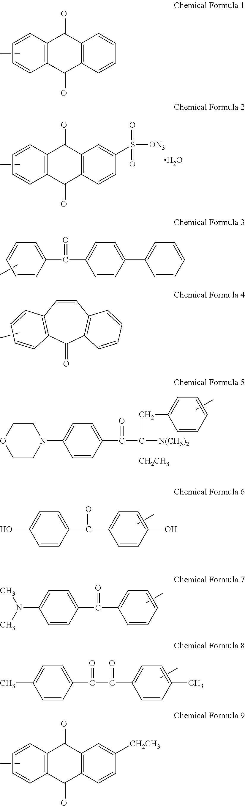
- the photoreactive group may include a group represented by one of the following Chemical Formula 1 to Chemical Formula 12:
- the reactive mesogen may include a compound represented by the following Chemical Formula 13: R1-S1-P1-E-P2-S2-R2 Chemical Formula 13
- R1 and R2 may each independently include an acrylate or a methacrylate
- S1 and S2 may each independently include a substituted or non-substituted C1 to C4 alkylene group or a single bond
- P1 and P2 may each independently include a substituted or non-substituted
- E may include —O—, —S—, —CO—, —CO—O—, —OCO—, —O—CO—O—, —OCH 2 —, —CH 2 O—, —COO—, —O—CH 2 —CH 2 —O—, or a single bond.
- the reactive mesogen may include a compound represented as given in Chemical Formula 14 to Chemical Formula 21:
- the light wavelength range may be about 250 nm to about 450 nm.
- a pre-tilt angle of a liquid crystal molecule that is adjacent to the first alignment layer may be greater than that of a liquid crystal molecule that is adjacent to the second alignment layer.
- the liquid crystal display may be a curved display.
- the second polymer may include a second main chain and a plurality of second side chains connected to the second main chain, and at least one of the plurality of second side chains may include a vertical alignment group.
- At least one of the plurality of first side chains may further include a vertical alignment group.
- the liquid crystal display may further include a thin film transistor between the first substrate and the first alignment layer; a pixel electrode connected with the thin film transistor; and a common electrode forming an electric field with the pixel electrode.
- the embodiments may be realized by providing a method of manufacturing a liquid crystal display, the method including preparing a lower panel including a first alignment layer on a first substrate; preparing an upper panel including a second alignment layer on a second substrate; forming a liquid crystal layer between the lower panel and the upper panel such that the liquid crystal layer includes a plurality of liquid crystal molecules; and irradiating light to the lower panel, the upper panel, and the liquid crystal layer, which are bonded to each other, wherein irradiating the light includes irradiating light to a photoreactive group of a first polymer and a reactive mesogen of the first alignment layer to form protrusions including an alignment polymer polymerized from the reactive mesogen, and wherein the photoreactive group has a higher absorbance than the reactive mesogen within a wavelength range of the irradiated light.
- the first polymer may include a first main chain, and a plurality of first side chains connected to the first main chain, at least one of the plurality of first side chains including the photoreactive group or a photoreactive derivative group
- the second alignment layer may include a second polymer, the second polymer including a second main chain and a plurality of second side chains connected to the second main chain, at least one of the plurality of second side chains including a vertical alignment group.
- the photoreactive group may include a group represented by one of the following Chemical Formula 1 to Chemical Formula 12:
- the reactive mesogen may include a compound represented by the following Chemical Formula 13: R1-S1-P1-E-P2-S2-R2 Chemical Formula 13
- R1 and R2 may each independently include one of acrylate and methacrylate
- S1 and S2 may each independently include a substituted or non-substituted C1 to C4 alkylene group or a single bond
- P1 and P2 may each independently include a substituted or non-substituted
- E may include one of —O—, —S—, —CO—, —CO—O—, —OCO—, —O—CO—O—, —OCH 2 —, —CH 2 O—, —COO—, —O—CH 2 —CH 2 —O—, or a single bond.
- the reactive mesogen may include a compound represented by one of the following Chemical Formula 14 to Chemical Formula 21:
- a pre-tilt angle of a liquid crystal molecule that is adjacent to the first alignment layer may be greater than a pre-tilt angle of a liquid crystal molecule that is adjacent to the second alignment layer.
- the liquid crystal display may be a curved display.
- the light wavelength range may be about 250 nm to about 450 nm.
- the embodiments may be realized by providing a liquid crystal display including a first substrate; a second substrate overlapping the first substrate at a distance therefrom; a liquid crystal layer between the first substrate and the second substrate, the liquid crystal layer including a plurality of liquid crystal molecules; a first alignment layer between the first substrate and the liquid crystal layer, the first alignment layer including a first polymer; and a second alignment layer between the second substrate and the liquid crystal layer, the second alignment layer including a second polymer, wherein a pre-tilt angle of a liquid crystal molecule that is adjacent to the first alignment layer is greater than that of a liquid crystal molecule that is adjacent to the second alignment layer, the first polymer includes a first main chain and a plurality of first side chains connected to the first main chain, at least one of the plurality of first side chains including a photoreactive group or a photoreactive derivative group, and the photoreactive group includes a group represented by one of the following Chemical Formula B1 or Chemical Formula B2:
- Cy may be a C6 to C18 aryl group or a C6 to C18 cycloalkyl group
- R 11 to R 14 may each independently include hydrogen or a substituted or unsubstituted C1 to C8 alkyl group
- R 15 and R 16 may each independently include a hydroxy group or a substituted or unsubstituted C1 to C8 alkoxy group
- R 17 may be hydrogen, a hydroxy group, or a substituted or unsubstituted C1 to C8 alkoxy group
- c and d may each independently be integers of 0 to 4
- k1 and k3 may each independently be integers of 3 to 20
- k2 may be an integer of 0 to 5
- Z1 and Z2 may be —C( ⁇ O)—
- Z3 may be —S— or —C( ⁇ O)—.
- the liquid crystal display may further include a plurality of protrusions between the first alignment layer and the liquid crystal layer, wherein at least one of the plurality of protrusions includes an alignment polymer polymerized from a reactive mesogen, and the first polymer has a reactivity in response to being exposed to light within a light wavelength range for forming the alignment polymer that is greater than a reactivity of the reactive mesogen within the light wavelength range.
- the reactive mesogen may include a compound represented by the following Chemical Formula 13: R1-S1-P1-E-P2-S2-R2 Chemical Formula 13
- R1 and R2 may each independently include an acrylate or a methacrylate
- S1 and S2 may each independently include a substituted or non-substituted C1 to C4 alkylene group or a single bond
- P1 and P2 may each independently include a substituted or non-substituted
- E may include —O—, —S—, —CO—, —CO—O—, —OCO—, —O—CO—O—, —OCH 2 —, —CH 2 O—, —COO—, —O—CH 2 —CH 2 —O—, or a single bond.
- the reactive mesogen may include a compound represented as given in Chemical Formula 14 to Chemical Formula 21:
- FIG. 1 illustrates a schematic perspective view of a curved liquid crystal display according to an exemplary embodiment.
- FIG. 2 illustrates a cross-sectional view of FIG. 1 , taken along the line II-II.
- FIG. 3 illustrates a graph of absorbance of a photoreactive mesogen and a photoreactive group with respect to light wavelengths.
- FIG. 4 illustrates a top plan view of a pixel in the liquid crystal display according to the exemplary embodiment.
- FIG. 5 illustrates a cross-sectional view of FIG. 4 , taken along the line V-V.
- the phrase “in a plan view” means viewing a target portion from the top
- the phrase “in a cross-section” means viewing a cross-section by vertically cutting a target portion from the side.
- substituted refers to at least one hydrogen atom being substituted or replaced by a substituent group of a halogen atom (F, Cl, Br, and I), a hydroxy group, a C1 to C20 alkoxy group, a nitro group, a cyano group, an amino group, an imino group, an azido group, an amidino group, a hydrazino group, a hydrazono group, a carbonyl group, a carbamyl group, a thiol group, an ester group, an ether group, a carboxyl group or a salt thereof, a sulfonic acid group or a salt thereof, a phosphoric acid or a salt thereof, a C1 to C20 alkyl group, a C2 to C20 alkenyl group, a C2 to C20 alkynyl group, a C6 to C30 aryl group, a C3 to
- hetero means that at least one heteroatom of N, O, S, and P is included in a cyclic group.
- alicyclic means C3 to C40 cycloalkyl, C3 to C40 cycloalkenyl, C3 to C40 cycloalkynyl, C3 to C40 cycloalkylene, C3 to C40 cycloalkenylene, or C3 to C40 cycloalkynylene, and specifically means C3 to C20 cycloalkyl, C3 to C20 cycloalkenyl, C3 to C20 cycloalkynyl, C3 to C20 cycloalkylene, C3 to C20 cycloalkenylene, or C3 to C20 cycloalkynylene, and the term “aromatic” means C6 to C40 aryl, C2 to C40 heteroaryl, C6 to C40 arylene, or C2 to C40 heteroarylene, and specifically means C6 to C16 aryl, C2 to C16 heteroaryl, C6 to C16 arylene
- the term “combination” generally means mixing or copolymerization, and means that in an alicyclic organic group and an aromatic organic group, two or more cycles form a fused cycle or two or more cycles are connected to each other by a group of a single bond, —O—, —S—, —C( ⁇ O)—, —CH(OH)—, —S( ⁇ O)—, —S( ⁇ O) 2 —, —Si(CH 3 ) 2 —, —(CH 2 )p- (herein, 1 ⁇ p ⁇ 2), —(CF 2 )q- (herein, 1 ⁇ q ⁇ 2), —C(CH 3 ) 2 —, —CH(CH 3 )—, —C(CF 3 ) 2 —, —CH(CF 3 )—, or —C( ⁇ O)NH—.
- copolymerization means block copolymerization or random copolymerization, and the
- FIG. 1 illustrates a schematic perspective view of a curved liquid crystal display according to an exemplary embodiment
- FIG. 2 illustrates a cross-sectional view of FIG. 1 taken along the line II-II
- FIG. 3 illustrates a graph of absorbance of a photoreactive mesogen and a photoreactive group with respect to light wavelengths.
- a liquid crystal display may be a curved type of liquid crystal display.
- a liquid crystal display 10 may be curved with reference to an axis that is parallel with a horizontal direction, which is the first direction in the drawing, or may be curved with reference to an axis that is parallel with a vertical direction, which is the second direction.
- the present specification describes a liquid crystal display curved with reference to an axis that is parallel with the second direction.
- the liquid crystal display can be curved in an axis that is parallel with the first direction.
- the liquid crystal display 10 may include a lower panel 100 , an upper panel 200 overlapping the lower panel 100 at a distance therefrom (e.g., the upper panel 200 may face and may be spaced apart from the lower panel 100 ), and a liquid crystal layer 3 between the lower panel 100 and the upper panel 200 .
- the liquid crystal layer 3 may include a plurality of liquid crystal molecules 31 .
- the lower panel 100 may include a first substrate 110 , a first alignment layer 11 between the first substrate 110 and the liquid crystal layer 3 , and a plurality of protrusions 13 between the first alignment layer 11 and the liquid crystal layer 3 .
- the protrusion 13 may include an alignment polymer polymerized with or from a reactive mesogen or may include an alignment polymer lump, which is the alignment polymer disposed adjacent to the surface of the first alignment layer 11 .
- liquid crystal molecules 31 adjacent to the first alignment layer 11 may have a pre-tilt. For example, even when the liquid crystal layer 3 is in a state in which no voltage is applied thereto, the liquid crystal molecules 31 that are adjacent to the first alignment layer 11 may be tilted with reference to a direction that is substantially perpendicular to one surface of the first alignment layer 11 due to the protrusions 13 .
- pre-tilt refers to the liquid crystal molecules 31 being tilted with reference to a direction that is perpendicular to one surface of the first alignment layer 11 or a second alignment layer 21 .
- Pre-tilt angle refers to the degree of tilting of the liquid crystal molecules 31 with respect to an axis that is perpendicular to the first alignment layer 11 or the second alignment layer 21 , e.g., a tilted angle.
- the upper panel 200 may include a second substrate 210 and the second alignment layer 21 between the second substrate 210 and the liquid crystal layer 3 .
- liquid crystal molecules 31 that are adjacent to the second alignment layer 21 may not have a pre-tilt.
- the liquid crystal molecules 31 that are adjacent to the second alignment layer 21 may be aligned substantially perpendicular to the surface of the second alignment layer 21 .
- the liquid crystal layer 3 between the lower panel 100 and the upper panel 200 may have negative dielectric anisotropy.
- first alignment layer 11 and the second alignment layer 21 will be described in detail.
- the first alignment layer 11 may include a first polymer.
- the first polymer may include, e.g., a first main chain and a plurality of side chains connected to the first main chain.
- the first main chain may include, e.g., a polyimide or the like.
- Each of the plurality of first side chains may include, e.g., a vertical alignment group, a photoreactive group, or a photoreactive derivative group.
- one side chain may include only one of the vertical alignment group, the photoreactive group, or the photoreactive derivative group.
- the vertical alignment group may be directly connected to the main chain and the photoreactive group and the photoreactive derivative group are coupled to the vertical alignment group.
- the term “or” is not an exclusive term such that “A or B” would include any and all combinations thereof, e.g., “A”, “B”, and “A and B”.
- the photoreactive derivative refers group to a similar compound or group acquired from transformation of a part of the photoreactive group.
- the photoreactive group may absorb energy from irradiated light to generate radicals that help polymerization of the reactive mesogen or may react with the reactive mesogen.
- the vertical alignment group may substantially perpendicularly align the liquid crystal molecules 31 that are adjacent to the first alignment layer 11 .
- the photoreactive group according to the present exemplary embodiment may include various materials that generate radicals or help polymerization.
- the photoreactive group may include a group represented by one of the following Chemical Formula 1 to Chemical Formula 12.
- the second alignment layer 21 may include a second polymer.
- the second polymer may be different from the first polymer.
- the second polymer may include, e.g., a second main chain and a plurality of second side chains connected to the second main chain.
- Each of the plurality of second side chains may include a vertical alignment group.
- the vertical alignment group may vertically align liquid crystal molecules 31 that are adjacent to the second alignment layer 21 .
- the second side chain may not include a photoreactive group or a photoreactive derivative group.
- the reactive mesogen may move to be adjacent to the light-irradiated photoreactive functional group.
- the second polymer may not include the photoreactive functional group, and the reactive mesogen may not be adjacent to the second alignment layer 21 .
- the protrusions 13 including the alignment polymer polymerized with the reactive mesogen may not be formed between the second alignment layer 21 and the liquid crystal layer 3 .
- the plurality of protrusions 13 may be between the first alignment layer 11 and the liquid crystal layer 3 and are may not be between second alignment layer 21 and the liquid crystal layer 3 .
- the protrusions 13 may protrude from one side of the first alignment layer 11 .
- the protrusions 13 may pre-tilt the liquid crystal molecules 31 that are adjacent to the first alignment layer 11 .
- the reactive mesogen mixed with the alignment material (e.g., including the first polymer) to form the first alignment layer 11 may be discharged or diffuse to the liquid crystal layer 3 during a baking process.
- a preliminary first alignment layer may include the reactive mesogen and the first polymer.
- the reactive mesogen may be polymerized by radicals from the photoreactive group such that an alignment polymer may be formed (e.g., of just the polymerized reactive mesogen), or the reactive mesogen and the photoreactive group of the first polymer may react with each other such that the alignment polymer (e.g., from both the reactive mesogen and the first polymer) may be formed.
- the protrusions 13 according to the exemplary embodiment may include such an alignment polymer or a lump where the alignment polymer is concentrated.
- the reactive mesogen may include, e.g., a compound represented by the following Chemical Formula 13. R1-S1-P1-E-P2-S2-R2 Chemical Formula 13
- R1 and R2 may each independently include, e.g., an acrylate or a methacrylate
- S1 and S2 may each independently include, e.g., a substituted or non-substituted C1 to C4 alkylene group or a single bond
- P1 and P2 may each independently include, e.g., a substituted or non-substituted
- R1 and P1 or R2 and P2 may be directly bonded without interposing an intermediate material therebetween.
- the compound represented by Chemical Formula 13 may include at least three rings.
- the reactive mesogen including at least three rings may have improved heat resistance, and when the alignment layers 11 and 21 are formed by curing the coated alignment material, the alignment layers 11 and 21 may be stable under a high-temperature heat treatment condition.
- the reactive mesogen may include, e.g., a compound represented by one of the following Chemical Formula 14 to 21.
- the reactive mesogen according to an embodiment may include the compound represented by Chemical Formula 13, and may be polymerized as an alignment polymer by light irradiation. At least one of the plurality of protrusions 13 may include such an alignment polymer or a lump of the alignment polymers.
- the plurality of protrusions 13 may be disposed only on the first alignment layer 11 , and may cause the liquid crystal molecules 31 adjacent to the first alignment layer 11 to be pre-tilted. In an implementation, no protrusion 13 may be provided between the second alignment layer 21 and the liquid crystal layer 3 , and the liquid crystal molecules 31 adjacent to the second alignment layer 21 may not be pre-tilted.
- the plurality of liquid crystal molecules 31 may be injected between the lower panel 100 and the upper panel 200 , and then a voltage may be applied and predetermined light (e.g., ultraviolet (UV)) may be irradiated thereto.
- predetermined light e.g., ultraviolet (UV)
- the above-stated photoreactive group may generate radicals or may be activated.
- the radicals or the activated photoreactive group may boost a polymerization reaction of the reactive mesogen, and the polymerized reactive mesogen may form an alignment polymer such that the plurality of protrusions 13 provided on the first alignment layer 11 are formed.
- the plurality of protrusions 13 may cause the liquid crystal molecules 31 that are adjacent to the first alignment layer 11 and the protrusions 13 to be pre-tilted.
- absorbance (denoted as b in FIG. 3 ) of the photoreactive group included in the first alignment layer 11 may be greater than absorbance (denoted as a in FIG. 3 ) of the reactive mesogen in a part of a wavelength range.
- the light wavelength range may be a suitable wavelength range for reaction between the photoreactive group and the reactive mesogen.
- the light wavelength range may be a light wavelength range for forming radicals from activation of the photoreactive group or forming the alignment polymer by activation of the reactive mesogen.
- the light wavelength range may be, e.g., a UV wavelength of about 250 nm to about 450 nm.
- a reaction at a predetermined wavelength (about 365 nm) shown in FIG. 3 will be exemplarily described.
- the radicals generated from the photoreactive group may be distributed or concentrated in an area that is adjacent to the first alignment layer 11 , or the activated photoreactive group may introduce or react with the reactive mesogen near the first alignment layer 11 .
- a polymerization reaction of the reactive mesogen may occur in the area that is adjacent to the first alignment layer 11 , and resultantly protrusions 13 (including the alignment polymer polymerized with or from the reactive mesogen) may be formed between the first alignment layer 11 and the liquid crystal layer 3 .
- the protrusions 13 may cause the liquid crystal molecules 31 disposed adjacent to the first alignment layer 11 to be pre-tilted.
- the second polymer that forms the second alignment layer 21 may not include an additional photoreactive functional group, and therefore, no reaction (such as generation of radicals or introduction of the reactive mesogen through an activated photoreactive group) may occur.
- no protrusion may be formed between the second alignment layer 21 and the liquid crystal layer 3 , and liquid crystal molecules 31 that are adjacent to the second alignment layer 21 may be vertically arranged rather than having a pre-tilt.
- the liquid crystal molecules 31 that are adjacent to the first alignment layer 11 may have the pre-tilt, and the liquid crystal molecules 31 that are adjacent to the second alignment layer 21 may not have the pre-tilt. Even if the lower panel 100 and the upper panel 200 were to be misaligned, the liquid crystal molecules 31 that are adjacent to the lower panel 100 and the liquid crystal molecules 31 that are adjacent to the upper panel 200 may not have directional misalignment therebetween, thereby controlling generation of a texture.
- the amount of radicals generated by the photoreactive group may be low, and a reaction for introducing or concentrating the reactive mesogen near to the first alignment layer 11 could weaken. Further, the reactive mesogen (which is in a state of being discharged to the liquid crystal layer 3 and then being activated) could move adjacent not only to the first alignment layer 11 but also to the second alignment layer 21 such that the reactive mesogen could be disposed not only between the first alignment layer 11 and the liquid crystal layer 3 but also between the second alignment layer 21 and the liquid crystal layer 3 .
- the protrusions 13 including the alignment polymer polymerized with or from the reactive mesogen could be disposed between the first alignment layer 11 and the liquid crystal layer 3 and between the second alignment layer 21 and the liquid crystal layer 3 .
- the liquid crystal molecules 31 that are adjacent to the first alignment layer 11 and the second alignment layer 21 may all have the pre-tilt.
- a flat display panel (where the liquid crystal molecules 31 have the pre-tilt in the same direction) were to be bent between the opposing lower and upper panels 100 and 200 , an area where the pre-tilt direction of the liquid crystal molecules 31 that are adjacent to the lower panel 100 and the pre-tilt direction of the liquid crystal molecules 31 that are adjacent to the upper panel 200 are mismatched could be formed. Such an area may occur at an interface between neighboring domains, and a texture fault could occur in the area.
- the first polymer (included in the first alignment layer 11 ) may include a first structure unit represented by the following Chemical Formula A and a second structure unit represented by the following Chemical Formula B.
- X 1 and X 2 may each independently be, e.g., tetravalent organic groups respectively induced from or including an alicyclic acid dianhydride or an aromatic acid dianhydride
- Y 1 may be, e.g., a divalent organic group induced from or including an aromatic diamine and at least one hydrogen of the divalent organic group may be substituted with a group represented by Chemical Formula A1
- Y 2 may be, e.g., a divalent organic group induced from or including an aromatic diamine, wherein at least hydrogen of the divalent organic group is substituted with a group represented by Chemical Formula B1 or Chemical Formula B2.
- R 1 to R 4 may each independently be or include, e.g., hydrogen or a substituted or unsubstituted C1 to C8 alkyl group
- n may be, e.g., an integer of 3 to 20
- R 5 may include, e.g., a substituted or unsubstituted C1 to C30 alkyl group
- a and b may each independently be, e.g., an integer of 0 to 4
- L 1 and L 2 may each independently be, e.g., a single bond, —O—, —S( ⁇ O) 2 —, or —(C(R x )(R y )) m —
- R x and R y may each independently be or include, e.g., a hydrogen atom or a substituted or unsubstituted C1 to C8 alkyl group
- m may be, e.g., an integer of 1 to 20).
- Y 1 is a divalent organic group induced from or including an aromatic diamine, and when at least one hydrogen of the divalent organic group is substituted with a group represented by Chemical Formula A1, the group represented by Chemical Formula A1 may function as a vertical aligner that vertically aligns the liquid crystal molecules 31 that are adjacent to the first alignment layer 11 .
- Cy may be, e.g., a C6 to C18 aryl group or a C6 to C18 cycloalkyl group
- R 11 to R 14 may each independently be or include, e.g., hydrogen or a substituted or unsubstituted C1 to C8 alkyl group
- R 15 and R 16 may each independently be or include, e.g., a hydroxy group or a substituted or unsubstituted C1 to C8 alkoxy group
- R 17 may be or may include, e.g., hydrogen, a hydroxy group, or a substituted or unsubstituted C1 to C8 alkoxy group
- c and d may each independently be, e.g., integers of 0 to 4
- k1 and k3 may each independently be, e.g., integers of 3 to 20
- k2 may be, e.g., an integer of 0 to 5
- Z1 and Z2 may be, e.
- the group represented by Chemical Formula B1 or Chemical Formula B2 may include or correspond with a photoreactive group or a photoreactive derivative group represented by Chemical Formula 1 to Chemical Formula 12.
- the second polymer included in the second alignment layer 21 may include a first structure unit represented by Chemical Formula A and may not include a second structure unit represented by Chemical Formula B.
- the second polymer may not include a photoreactive group or a photoreactive derivative group.
- the first polymer and the second polymer including the above-stated structure units may include a polyimide.
- the polyimide may be manufactured by manufacturing polyamic acid formed by copolymerizing at least one acid dianhydride selected from an alicyclic acid dianhydride and an aromatic acid dianhydride, and an aromatic diamine, and imidizing the polyamic acid.
- a method of manufacturing the polyamic acid a method suitable for synthesizing of the polyamic acid may be applied.
- the alicyclic acid dianhydride may include, e.g., 1,2,3,4-cyclobutanetetracarboxylic acid dianhydride (CBDA), 2,3,4,5-tetrahydrofurantetracarboxylic acid dianhydride, 5-(2,5-dioxotetrahydrofuryl)-3-methylcyclohexane-1,2-dicarboxylic anhydride (DOCDA), bicyclooctene-2,3,5,6-tetracarboxylic acid dianhydride (BODA), 1,2,3,4-cyclopentanetetracarboxylic dianhydride (CPDA), 1,2,4,5-cyclohexanetetracarboxylic acid dianhydride (CHDA), 1,2,4-tricarboxy-3-methylcarboxy cyclopentane dianhydride, 1,2,3,4-etracarboxy cyclopentane dianhydride, 3,4-dicarboxy-1-cyclohexyl succinic
- the aromatic acid dianhydride may include, e.g., pyromellitic acid dianhydride (PMDA), biphthalic acid anhydride (BPDA), oxydiphthalic acid dianhydride (ODPA), benzophenone tetracarboxylic acid dianhydride (BTDA), or (hexafluoroisopropylidene)diphthalic dianhydride (6-FDA).
- PMDA pyromellitic acid dianhydride
- BPDA biphthalic acid anhydride
- ODPA oxydiphthalic acid dianhydride
- BTDA benzophenone tetracarboxylic acid dianhydride
- 6-FDA hexafluoroisopropylidene
- the photoreactive group according to the exemplary embodiment may have higher light absorbance and/or higher reactivity than the photoreactive mesogen in a wavelength of light irradiated to the display device during a manufacturing process. Accordingly, reaction from the photoreactive group may be excellent compared to reaction from the reactive mesogen upon light irradiation. For example, the reaction of the photoreactive group may proceed at a higher rate than that of the reactive mesogen, upon light irradiation.
- a majority of radicals may be distributed or concentrated in an area that is adjacent to the first alignment layer 11 (that includes the first polymer having the photoreactive group), and reactive mesogen may form an alignment polymer at the periphery of the first alignment layer 11 or the activated photoreactive group may induce the reactive mesogen to be near the first alignment layer 11 such that the alignment polymer may be formed.
- a reaction for forming the protrusions 13 may be predominantly performed near the first alignment layer 11 , and the protrusions 13 may be formed only at the periphery of the first alignment layer 11 (and the protrusions 13 may not be formed at the periphery of the second alignment layer 21 ).
- liquid crystal display wherein the liquid crystal molecules that are adjacent to the first alignment layer 11 have a pre-tilt and the liquid crystal molecules that are adjacent to the second alignment layer 21 do not have a pre-tilt may be provided.
- the photoreactive group according to the exemplary embodiment may have excellent reactivity, most of the discharged reactive mesogen may form protrusions that include an alignment polymer or a lump of alignment polymers, and the plurality of protrusions may cause the liquid crystal molecules 31 that are adjacent to the first alignment layer 11 to be stably pre-tilted.
- the high-reactive photoreactive group may be included, time consumed in the manufacturing process may be reduced while reducing manufacturing cost, and productivity may be improved.
- FIG. 4 illustrates a top plan layout view of a pixel in the liquid crystal display according to the exemplary embodiment
- FIG. 5 illustrates a cross-sectional view of FIG. 4 , taken along the line V-V.
- the lower panel 100 will now be described.
- a gate conductor including gate lines 121 and divided reference voltage lines 131 may be provided on a first substrate 110 that is made of transparent glass or plastic.
- the gate line 121 may include a first gate electrode 124 a , a second gate electrode 124 b , and a third gate electrode 124 c.
- the divided reference voltage line 131 may include first sustain electrodes 135 and 136 and a reference electrode 137 . Although second storage electrodes 138 and 139 are not connected to the divided reference voltage line 131 , the second storage electrodes 138 and 139 may be disposed to be overlapped with a second sub-pixel electrode 191 b.
- a gate insulation layer 140 is provided on the gate line 121 and the divided reference voltage line 131 .
- a first semiconductor layer 154 a , a second semiconductor layer 154 b , and a third semiconductor layer 154 c may be provided on the gate insulating layer 140 .
- Ohmic contacts 163 a , 165 a , 163 b , 165 b , 163 c , and 165 c are provided on the semiconductor layers 154 a , 154 b , and 154 c.
- a data conductor including data lines 171 connected to a first source electrode 173 a and a second source electrode 173 b , a first drain electrode 175 a , a second drain electrode 175 b , a third source electrode 173 c , and a third drain electrode 175 c may be provided on the ohmic contacts 163 a , 165 a , 163 b , 165 b , 163 c , and 165 c and the gate insulating layer 140 .
- the first gate electrode 124 a , the first source electrode 173 a , and the first drain electrode 175 a may form a first thin film transistor, together with the first semiconductor layer 154 a , the second gate electrode 124 b , the second source electrode 173 b , and the second drain electrode 175 b may form a second thin film transistor, together with the second semiconductor layer 154 b , and the third gate electrode 124 c , the third source electrode 173 c , and the third drain electrode 175 c may form a third thin film transistor, together with the third semiconductor layer 154 c.
- the second drain electrode 175 b may be connected with the third source electrode 173 c , and includes a wide expansion portion 177 .
- a first passivation layer 180 p may be provided on portions of the data conductors 171 , 173 c , 175 a , 175 b , and 175 c and the semiconductor layers 154 a , 154 b , and 154 c.
- a color filter 230 may be provided on the first passivation layer 180 p .
- the color filter 230 may vertically extend along two adjacent data lines 171 .
- the color filter 230 may be included in, e.g., the lower panel 100 .
- the color filter 230 may be included in, e.g., the upper panel 200 .
- a second passivation layer 180 q may be provided on the color filter 230 .
- the first passivation layer 180 p and the second passivation layer 180 q may include an inorganic insulation layer such as a silicon nitride or a silicon oxide.
- the second passivation layer 180 q may help prevent the color filter 230 from being lifted, and may help control contamination of the liquid crystal layer 3 caused by organic materials such as a solvent input by the color filters 230 , in order to prevent faults such as an afterimage that may be induced when a screen is driven.
- the first passivation layer 180 p and second passivation layer 180 q may include a first contact hole 185 a and a second contact hole 185 b that expose the first drain electrode 175 a and the second drain electrode 175 b.
- the first passivation layer 180 p , the second passivation layer 180 q , and the gate insulating layer 140 may include a third contact hole 185 c that partially exposes the reference electrode 137 and the third drain electrode 175 c , and the third contact hole 185 c may be covered by a connection member 195 .
- the connection member 195 may electrically connect the reference electrode 137 and the third drain electrode 175 , which are partially exposed through the third contact hole 185 c , to each other.
- a pixel electrode 191 may be provided on the second passivation layer 180 q .
- the pixel electrode 191 may be one of field generating electrodes, and each pixel electrode 191 may be separated, interposing the gate line 121 therebetween, and thus includes a first sub-pixel electrode 191 a and a second sub-pixel electrode 191 b that neighbor each other in a column direction with reference to the gate line 121 .
- the pixel electrode 191 may be made of a transparent material such as ITO and IZO.
- the entire shape of the first sub-pixel electrode 191 a and the second sub-pixel electrode 191 b may be quadrangular, and the first and second sub-pixel electrodes 191 a and 191 b may respectively include a cross stem formed of a horizontal stem 193 and a vertical stem 192 that perpendicularly crosses the horizontal stem 193 .
- each of the first sub-pixel 191 a and the second sub-pixel 191 b may be divided into a first sub-region DA, a second sub-region Db, a third sub-region Dc, and a fourth sub-region Dd by the horizontal stem 193 and the vertical stem 192 , and may include a plurality of minute branches 194 provided in the respective sub-regions Da to Dd.
- the first sub-pixel electrode 191 a and the second sub-pixel electrode 191 b may be respectively connected with the first drain electrode 175 a or the second drain electrode 175 b through the first contact hole 185 a and the second contact hole 185 b , and receive a data voltage from the first drain electrode 175 a and the second drain electrode 175 b .
- a part of the data voltage applied to the second drain electrode 175 b may be divided through the third source electrode 173 c such that the voltage applied to the first sub-pixel electrode 191 a becomes greater than the voltage applied to the second sub-pixel electrode 191 b.
- the first sub-pixel electrode 191 a and the second sub-pixel electrode 191 b applied with the data voltage may generate an electric field together with a common electrode 270 of the upper panel 200 such that a direction of the liquid crystal molecules 31 of the liquid crystal layer 3 disposed between the two electrodes 191 and 270 may be determined. Depending on the direction of the liquid crystal molecules 31 , luminance of light passing through the liquid crystal layer 3 may be changed.
- the description of the thin film transistors and the pixel electrode 191 described above is one example, and the structure of the thin film transistors and the design of the pixel electrode may be modified to enhance side visibility rather than being restricted to the above-described structure.
- a first alignment layer 11 may be provided on the pixel electrode 191 , and the first alignment layer 11 may be the above-stated first alignment layer 11 which has been described with reference to FIG. 1 to FIG. 3 .
- the second substrate 210 may be disposed to be overlapped with the first substrate 110 at a distance therefrom.
- a light blocking member 220 may be provided between the second substrate 210 and the liquid crystal layer 3 .
- the light blocking member 220 may be provided in the upper panel 200 so as to overlap an area where the data line 171 of the lower panel 100 is disposed and an area where the thin film transistor is disposed.
- the light blocking member 220 may be included in the upper panel 200 .
- the light blocking member 220 may be included in the lower panel 100 .
- An overcoat 250 may be disposed between the light blocking member 220 and the liquid crystal layer 3 .
- the overcoat 250 may be omitted.
- the common electrode 270 which is one of the field generating electrodes, may be provided between the overcoat 250 and the liquid crystal layer 3 .
- the common electrode 270 may generate an electric field together with the pixel electrode 191 of the lower panel 100 such that a direction of the liquid crystal molecules 31 of the liquid crystal layer 3 may be determined.
- a second alignment layer 21 may be provided between the common electrode 270 and the liquid crystal layer 3 , and the second alignment layer 21 may be the above-stated second alignment layer 21 which has been described with reference to FIG. 1 to FIG. 3 .
- the liquid crystal layer 3 including a plurality of liquid crystal molecules 31 may be disposed between the first alignment layer 11 and the second alignment layer 21 , and the liquid crystal layer 3 may have negative dielectric anisotropy.
- liquid crystal displays are becoming wider, and curved display devices are being developed to enhance immersion and realism of viewers.
- the embodiment provide a liquid crystal display that may help reduce and/or prevent deterioration of transmittance due to misalignment of an upper panel and a lower panel and may help control generation of a stain and a texture in the display panel.
- deterioration of transmittance due to misalignment of an upper panel and a lower panel may be reduced and/or prevented, and generation of a stain and a texture in the display panel may be reduced and/or prevented.
Landscapes
- Physics & Mathematics (AREA)
- Chemical & Material Sciences (AREA)
- Nonlinear Science (AREA)
- Crystallography & Structural Chemistry (AREA)
- General Physics & Mathematics (AREA)
- Mathematical Physics (AREA)
- Optics & Photonics (AREA)
- Spectroscopy & Molecular Physics (AREA)
- Engineering & Computer Science (AREA)
- Materials Engineering (AREA)
- Organic Chemistry (AREA)
- Microelectronics & Electronic Packaging (AREA)
- Geometry (AREA)
- Liquid Crystal (AREA)
Abstract
Description


R1-S1-P1-E-P2-S2-R2 Chemical Formula 13
or a substituted or non-substituted
and E may include —O—, —S—, —CO—, —CO—O—, —OCO—, —O—CO—O—, —OCH2—, —CH2O—, —COO—, —O—CH2—CH2—O—, or a single bond.


R1-S1-P1-E-P2-S2-R2 Chemical Formula 13
or a substituted or non-substituted
and E may include one of —O—, —S—, —CO—, —CO—O—, —OCO—, —O—CO—O—, —OCH2—, —CH2O—, —COO—, —O—CH2—CH2—O—, or a single bond.


R1-S1-P1-E-P2-S2-R2 Chemical Formula 13
or a substituted or non-substituted
and E may include —O—, —S—, —CO—, —CO—O—, —OCO—, —O—CO—O—, —OCH2—, —CH2O—, —COO—, —O—CH2—CH2—O—, or a single bond.


R1-S1-P1-E-P2-S2-
or a substituted or non-substituted
and E may include, e.g., —O—, —S—, —CO—, —CO—O—, —OCO—, —O—CO—O—, —OCH2—, —CH2O—, —COO—, —O—CH2—CH2—O—, or a single bond. When S1 and S2 are single bonds, R1 and P1 or R2 and P2 may be directly bonded without interposing an intermediate material therebetween.


Claims (20)


R1-S1-P1-E-P2-S2-R2 Chemical Formula 13


R1-S1-P1-E-P2-S2-R2 Chemical Formula 13


R1-S1-P1-E-P2-S2-R2 Chemical Formula 13

Applications Claiming Priority (2)
| Application Number | Priority Date | Filing Date | Title |
|---|---|---|---|
| KR10-2016-0066147 | 2016-05-30 | ||
| KR1020160066147A KR20170136029A (en) | 2016-05-30 | 2016-05-30 | Liquid crystal display and manufacturing method thereof |
Publications (2)
| Publication Number | Publication Date |
|---|---|
| US20170343862A1 US20170343862A1 (en) | 2017-11-30 |
| US10564480B2 true US10564480B2 (en) | 2020-02-18 |
Family
ID=60417773
Family Applications (1)
| Application Number | Title | Priority Date | Filing Date |
|---|---|---|---|
| US15/353,757 Expired - Fee Related US10564480B2 (en) | 2016-05-30 | 2016-11-17 | Liquid crystal display and manufacturing method thereof |
Country Status (3)
| Country | Link |
|---|---|
| US (1) | US10564480B2 (en) |
| KR (1) | KR20170136029A (en) |
| CN (1) | CN107450235A (en) |
Families Citing this family (2)
| Publication number | Priority date | Publication date | Assignee | Title |
|---|---|---|---|---|
| KR102611868B1 (en) * | 2016-06-02 | 2023-12-11 | 삼성디스플레이 주식회사 | Liquid crystal display and manufacturing method thereof |
| US11053354B2 (en) * | 2018-07-23 | 2021-07-06 | Sharp Kabushiki Kaisha | Liquid crystal display device |
Citations (11)
| Publication number | Priority date | Publication date | Assignee | Title |
|---|---|---|---|---|
| US20080013292A1 (en) * | 2004-03-16 | 2008-01-17 | Koninklijke Philips Electronics, N.V. | Rollable Electronic Panel Device |
| US20100149446A1 (en) * | 2007-03-30 | 2010-06-17 | Dic Corporation | Polymer-stabilized liquid crystal composition, liquid crystal display device, method for producing liquid crystal display device |
| US20120092603A1 (en) * | 2009-06-29 | 2012-04-19 | Masanobu Mizusaki | Liquid crystal display device and manufacturing method therefor |
| US20120218500A1 (en) * | 2011-02-25 | 2012-08-30 | Sony Corporation | Liquid crystal display device and manufacturing method thereof |
| WO2013183684A1 (en) * | 2012-06-06 | 2013-12-12 | Dic株式会社 | Liquid-crystal optical modulation element |
| KR20140073483A (en) | 2012-10-12 | 2014-06-16 | 디아이씨 가부시끼가이샤 | Liquid crystal composition and liquid crystal display device using the same |
| US8830428B2 (en) | 2009-12-09 | 2014-09-09 | Sony Corporation | Liquid crystal display element and liquid crystal display device |
| KR20140132206A (en) | 2013-05-07 | 2014-11-17 | 애경화학 주식회사 | New Reactive Mesogen Compound having asymmetric linkage structure and the Method for Manufacturing the Same |
| US20140375939A1 (en) * | 2013-06-25 | 2014-12-25 | Shenzhen China Star Optoelectronics Technology Co., Ltd. | Alignment Film, A Method of Fabricating The Same, and A Liquid Crystal Display Using The Same |
| KR20150012093A (en) | 2013-07-24 | 2015-02-03 | 삼성디스플레이 주식회사 | Liquid crystal display and manufacturing method thereof |
| KR20150130801A (en) | 2014-05-14 | 2015-11-24 | 동아대학교 산학협력단 | L c d with controllable surface anchoring energy and method for fabricating l c d, and manufacturing device for l c d |
Family Cites Families (4)
| Publication number | Priority date | Publication date | Assignee | Title |
|---|---|---|---|---|
| AU2011265294B2 (en) * | 2010-06-10 | 2015-01-22 | Aquestive Therapeutics, Inc. | Nanoparticle film delivery systems |
| CN103254356B (en) * | 2013-04-25 | 2016-01-13 | 深圳市华星光电技术有限公司 | Polymerizable mixture and liquid-crystal composition thereof |
| EP2963489B1 (en) * | 2014-06-30 | 2019-06-19 | Samsung Display Co., Ltd. | Curved display device |
| KR20160108718A (en) * | 2015-03-05 | 2016-09-20 | 삼성디스플레이 주식회사 | Liquid crystal display device and method of manufacturing the same |
-
2016
- 2016-05-30 KR KR1020160066147A patent/KR20170136029A/en not_active Withdrawn
- 2016-11-17 US US15/353,757 patent/US10564480B2/en not_active Expired - Fee Related
-
2017
- 2017-02-06 CN CN201710065570.2A patent/CN107450235A/en active Pending
Patent Citations (14)
| Publication number | Priority date | Publication date | Assignee | Title |
|---|---|---|---|---|
| US20080013292A1 (en) * | 2004-03-16 | 2008-01-17 | Koninklijke Philips Electronics, N.V. | Rollable Electronic Panel Device |
| US20100149446A1 (en) * | 2007-03-30 | 2010-06-17 | Dic Corporation | Polymer-stabilized liquid crystal composition, liquid crystal display device, method for producing liquid crystal display device |
| US20120092603A1 (en) * | 2009-06-29 | 2012-04-19 | Masanobu Mizusaki | Liquid crystal display device and manufacturing method therefor |
| US8830428B2 (en) | 2009-12-09 | 2014-09-09 | Sony Corporation | Liquid crystal display element and liquid crystal display device |
| US20120218500A1 (en) * | 2011-02-25 | 2012-08-30 | Sony Corporation | Liquid crystal display device and manufacturing method thereof |
| US8619222B2 (en) | 2011-02-25 | 2013-12-31 | Sony Corporation | Liquid crystal display device and manufacturing method thereof |
| US20160017226A1 (en) * | 2012-06-06 | 2016-01-21 | Dic Corporation | Liquid-crystal optical modulation element |
| WO2013183684A1 (en) * | 2012-06-06 | 2013-12-12 | Dic株式会社 | Liquid-crystal optical modulation element |
| KR20140073483A (en) | 2012-10-12 | 2014-06-16 | 디아이씨 가부시끼가이샤 | Liquid crystal composition and liquid crystal display device using the same |
| EP2824161A1 (en) | 2012-10-12 | 2015-01-14 | DIC Corporation | Liquid-crystal composition and liquid-crystal display element obtained using same |
| KR20140132206A (en) | 2013-05-07 | 2014-11-17 | 애경화학 주식회사 | New Reactive Mesogen Compound having asymmetric linkage structure and the Method for Manufacturing the Same |
| US20140375939A1 (en) * | 2013-06-25 | 2014-12-25 | Shenzhen China Star Optoelectronics Technology Co., Ltd. | Alignment Film, A Method of Fabricating The Same, and A Liquid Crystal Display Using The Same |
| KR20150012093A (en) | 2013-07-24 | 2015-02-03 | 삼성디스플레이 주식회사 | Liquid crystal display and manufacturing method thereof |
| KR20150130801A (en) | 2014-05-14 | 2015-11-24 | 동아대학교 산학협력단 | L c d with controllable surface anchoring energy and method for fabricating l c d, and manufacturing device for l c d |
Also Published As
| Publication number | Publication date |
|---|---|
| US20170343862A1 (en) | 2017-11-30 |
| CN107450235A (en) | 2017-12-08 |
| KR20170136029A (en) | 2017-12-11 |
Similar Documents
| Publication | Publication Date | Title |
|---|---|---|
| US9723769B2 (en) | Liquid crystal display device, alignment film, and methods for manufacturing the same | |
| KR102069822B1 (en) | Liquid crystal display and manufacturing method thereof | |
| KR100913605B1 (en) | Liquid crystal photo-alignment agent, liquid crystal photo-alignment layer comprising the same, and liquid crystal display device comprising the same | |
| US8865274B2 (en) | Liquid crystal display device, alignment film, and methods for manufacturing the same | |
| CN102122103B (en) | Liquid crystal display element and liquid crystal display device | |
| KR20110111212A (en) | Pixel electrode display panel, liquid crystal panel assembly and methods of manufacturing the same | |
| US9360709B2 (en) | Liquid crystal display device | |
| CN107703681B (en) | Liquid crystal display and method of manufacturing the same | |
| US20160259211A1 (en) | Curved liquid crystal display and method of manufacturing the same | |
| KR102456697B1 (en) | Liquid crystal display and manufacturing method thereof | |
| US20160259212A1 (en) | Liquid crystal display and manufacturing method thereof | |
| US10564480B2 (en) | Liquid crystal display and manufacturing method thereof | |
| KR102224841B1 (en) | Liquid crystal display device and method for manufacturing the same | |
| US9977288B2 (en) | Liquid crystal display | |
| KR20170010242A (en) | Liquid crystal display | |
| US10338435B2 (en) | Liquid crystal display device having upper and lower alignment layers | |
| EP3076233B1 (en) | Polymeric alignment layers in a curved vertically-aligned liquid crystal display | |
| KR101333708B1 (en) | Liquid crystal alignment agent, liquid crystal alignment film manufactured using the same, and liquid crystal display device including the liquid crystal alignment film | |
| US10745622B2 (en) | Alignment layer composition, liquid crystal display including the alignment layer composition, and manufacturing method of the liquid crystal display | |
| CN107463028B (en) | Liquid crystal display and method of manufacturing the same | |
| KR20120076415A (en) | Liquid crystal alignment agent, liquid crystal alignment film manufactured using the same, and liquid crystal display device including the liquid crystal alignment film | |
| KR20170121025A (en) | Composition for alignment layer and liquid crystal display including the same and method for manufacturing the liquid crystal display | |
| KR20130067734A (en) | Liquid crystal alignment agent, liquid crystal alignment film manufactured using the same, and liquid crystal display device including the liquid crystal alignment film |
Legal Events
| Date | Code | Title | Description |
|---|---|---|---|
| AS | Assignment |
Owner name: SAMSUNG DISPLAY CO., LTD., KOREA, REPUBLIC OF Free format text: ASSIGNMENT OF ASSIGNORS INTEREST;ASSIGNORS:KWON, OH JEONG;LEE, HYEOK JIN;KIM, KA EUN;AND OTHERS;REEL/FRAME:040350/0256 Effective date: 20161021 |
|
| STPP | Information on status: patent application and granting procedure in general |
Free format text: NON FINAL ACTION MAILED |
|
| STPP | Information on status: patent application and granting procedure in general |
Free format text: FINAL REJECTION MAILED |
|
| STPP | Information on status: patent application and granting procedure in general |
Free format text: ADVISORY ACTION MAILED |
|
| STPP | Information on status: patent application and granting procedure in general |
Free format text: DOCKETED NEW CASE - READY FOR EXAMINATION |
|
| STPP | Information on status: patent application and granting procedure in general |
Free format text: NOTICE OF ALLOWANCE MAILED -- APPLICATION RECEIVED IN OFFICE OF PUBLICATIONS |
|
| STPP | Information on status: patent application and granting procedure in general |
Free format text: PUBLICATIONS -- ISSUE FEE PAYMENT RECEIVED |
|
| STCF | Information on status: patent grant |
Free format text: PATENTED CASE |
|
| FEPP | Fee payment procedure |
Free format text: MAINTENANCE FEE REMINDER MAILED (ORIGINAL EVENT CODE: REM.); ENTITY STATUS OF PATENT OWNER: LARGE ENTITY |
|
| LAPS | Lapse for failure to pay maintenance fees |
Free format text: PATENT EXPIRED FOR FAILURE TO PAY MAINTENANCE FEES (ORIGINAL EVENT CODE: EXP.); ENTITY STATUS OF PATENT OWNER: LARGE ENTITY |
|
| STCH | Information on status: patent discontinuation |
Free format text: PATENT EXPIRED DUE TO NONPAYMENT OF MAINTENANCE FEES UNDER 37 CFR 1.362 |
|
| FP | Lapsed due to failure to pay maintenance fee |
Effective date: 20240218 |