US10559674B2 - Manufacturing method of a trench power semiconductor device - Google Patents
Manufacturing method of a trench power semiconductor device Download PDFInfo
- Publication number
- US10559674B2 US10559674B2 US15/988,018 US201815988018A US10559674B2 US 10559674 B2 US10559674 B2 US 10559674B2 US 201815988018 A US201815988018 A US 201815988018A US 10559674 B2 US10559674 B2 US 10559674B2
- Authority
- US
- United States
- Prior art keywords
- layer
- trench
- forming
- dielectric layer
- spacing
- Prior art date
- Legal status (The legal status is an assumption and is not a legal conclusion. Google has not performed a legal analysis and makes no representation as to the accuracy of the status listed.)
- Active, expires
Links
Images


Classifications
-
- H01L29/66734—
-
- H01L29/407—
-
- H01L29/4236—
-
- H01L29/7813—
-
- H—ELECTRICITY
- H10—SEMICONDUCTOR DEVICES; ELECTRIC SOLID-STATE DEVICES NOT OTHERWISE PROVIDED FOR
- H10D—INORGANIC ELECTRIC SEMICONDUCTOR DEVICES
- H10D30/00—Field-effect transistors [FET]
- H10D30/01—Manufacture or treatment
- H10D30/021—Manufacture or treatment of FETs having insulated gates [IGFET]
- H10D30/028—Manufacture or treatment of FETs having insulated gates [IGFET] of double-diffused metal oxide semiconductor [DMOS] FETs
- H10D30/0291—Manufacture or treatment of FETs having insulated gates [IGFET] of double-diffused metal oxide semiconductor [DMOS] FETs of vertical DMOS [VDMOS] FETs
- H10D30/0297—Manufacture or treatment of FETs having insulated gates [IGFET] of double-diffused metal oxide semiconductor [DMOS] FETs of vertical DMOS [VDMOS] FETs using recessing of the gate electrodes, e.g. to form trench gate electrodes
-
- H—ELECTRICITY
- H10—SEMICONDUCTOR DEVICES; ELECTRIC SOLID-STATE DEVICES NOT OTHERWISE PROVIDED FOR
- H10D—INORGANIC ELECTRIC SEMICONDUCTOR DEVICES
- H10D30/00—Field-effect transistors [FET]
- H10D30/60—Insulated-gate field-effect transistors [IGFET]
- H10D30/64—Double-diffused metal-oxide semiconductor [DMOS] FETs
- H10D30/66—Vertical DMOS [VDMOS] FETs
- H10D30/668—Vertical DMOS [VDMOS] FETs having trench gate electrodes, e.g. UMOS transistors
-
- H—ELECTRICITY
- H10—SEMICONDUCTOR DEVICES; ELECTRIC SOLID-STATE DEVICES NOT OTHERWISE PROVIDED FOR
- H10D—INORGANIC ELECTRIC SEMICONDUCTOR DEVICES
- H10D64/00—Electrodes of devices having potential barriers
- H10D64/111—Field plates
- H10D64/117—Recessed field plates, e.g. trench field plates or buried field plates
-
- H—ELECTRICITY
- H10—SEMICONDUCTOR DEVICES; ELECTRIC SOLID-STATE DEVICES NOT OTHERWISE PROVIDED FOR
- H10D—INORGANIC ELECTRIC SEMICONDUCTOR DEVICES
- H10D64/00—Electrodes of devices having potential barriers
- H10D64/20—Electrodes characterised by their shapes, relative sizes or dispositions
- H10D64/27—Electrodes not carrying the current to be rectified, amplified, oscillated or switched, e.g. gates
- H10D64/311—Gate electrodes for field-effect devices
- H10D64/411—Gate electrodes for field-effect devices for FETs
- H10D64/511—Gate electrodes for field-effect devices for FETs for IGFETs
- H10D64/512—Disposition of the gate electrodes, e.g. buried gates
- H10D64/513—Disposition of the gate electrodes, e.g. buried gates within recesses in the substrate, e.g. trench gates, groove gates or buried gates
-
- H—ELECTRICITY
- H10—SEMICONDUCTOR DEVICES; ELECTRIC SOLID-STATE DEVICES NOT OTHERWISE PROVIDED FOR
- H10D—INORGANIC ELECTRIC SEMICONDUCTOR DEVICES
- H10D64/00—Electrodes of devices having potential barriers
- H10D64/20—Electrodes characterised by their shapes, relative sizes or dispositions
- H10D64/27—Electrodes not carrying the current to be rectified, amplified, oscillated or switched, e.g. gates
- H10D64/311—Gate electrodes for field-effect devices
- H10D64/411—Gate electrodes for field-effect devices for FETs
- H10D64/511—Gate electrodes for field-effect devices for FETs for IGFETs
- H10D64/517—Gate electrodes for field-effect devices for FETs for IGFETs characterised by the conducting layers
- H10D64/518—Gate electrodes for field-effect devices for FETs for IGFETs characterised by the conducting layers characterised by their lengths or sectional shapes
-
- H—ELECTRICITY
- H10—SEMICONDUCTOR DEVICES; ELECTRIC SOLID-STATE DEVICES NOT OTHERWISE PROVIDED FOR
- H10D—INORGANIC ELECTRIC SEMICONDUCTOR DEVICES
- H10D64/00—Electrodes of devices having potential barriers
- H10D64/60—Electrodes characterised by their materials
- H10D64/66—Electrodes having a conductor capacitively coupled to a semiconductor by an insulator, e.g. MIS electrodes
- H10D64/68—Electrodes having a conductor capacitively coupled to a semiconductor by an insulator, e.g. MIS electrodes characterised by the insulator, e.g. by the gate insulator
- H10D64/681—Electrodes having a conductor capacitively coupled to a semiconductor by an insulator, e.g. MIS electrodes characterised by the insulator, e.g. by the gate insulator having a compositional variation, e.g. multilayered
- H10D64/685—Electrodes having a conductor capacitively coupled to a semiconductor by an insulator, e.g. MIS electrodes characterised by the insulator, e.g. by the gate insulator having a compositional variation, e.g. multilayered being perpendicular to the channel plane
-
- H—ELECTRICITY
- H10—SEMICONDUCTOR DEVICES; ELECTRIC SOLID-STATE DEVICES NOT OTHERWISE PROVIDED FOR
- H10D—INORGANIC ELECTRIC SEMICONDUCTOR DEVICES
- H10D62/00—Semiconductor bodies, or regions thereof, of devices having potential barriers
- H10D62/10—Shapes, relative sizes or dispositions of the regions of the semiconductor bodies; Shapes of the semiconductor bodies
- H10D62/17—Semiconductor regions connected to electrodes not carrying current to be rectified, amplified or switched, e.g. channel regions
- H10D62/393—Body regions of DMOS transistors or IGBTs
-
- H—ELECTRICITY
- H10—SEMICONDUCTOR DEVICES; ELECTRIC SOLID-STATE DEVICES NOT OTHERWISE PROVIDED FOR
- H10D—INORGANIC ELECTRIC SEMICONDUCTOR DEVICES
- H10D64/00—Electrodes of devices having potential barriers
- H10D64/20—Electrodes characterised by their shapes, relative sizes or dispositions
- H10D64/23—Electrodes carrying the current to be rectified, amplified, oscillated or switched, e.g. sources, drains, anodes or cathodes
- H10D64/251—Source or drain electrodes for field-effect devices
- H10D64/252—Source or drain electrodes for field-effect devices for vertical or pseudo-vertical devices
- H10D64/2527—Source or drain electrodes for field-effect devices for vertical or pseudo-vertical devices for vertical devices wherein the source or drain electrodes are recessed in semiconductor bodies
Definitions
- the present disclosure relates to a manufacturing method of a trench power semiconductor device; more particularly, to a manufacturing method of a trench power semiconductor device with shielding electrodes.
- the work losses of current power metal oxide semiconductor field transistors can be classified into two main categories: switching loss and conducting loss.
- the gate/drain capacitance (Cgd) is an important parameter that can severely affect the switching loss. If the Cgd is too high, it will result in an increase in the switching loss, which in turn limits the switching speed of the power MOSFETs so that it may be harmful for the power MOSFETs to be used in high frequency circuits.
- a manufacturing method of a trench power semiconductor device in which a protective layer and a spacing layer are formed on a surface of an epitaxial layer and a sidewall of a trench. According to such disclosure, the surface of the epitaxial layer and the sidewall of the trench will not be oxidized during the thermal oxidation process.
- the manufacturing method of a trench power semiconductor device includes forming an epitaxial layer on a substrate, forming a protective layer on a surface of the epitaxial layer, forming a trench in the epitaxial layer; and forming a trench gate structure in the trench, in which the trench gate structure includes a shielding electrode, a gate disposed on the shielding electrode and an inter-electrode dielectric layer disposed between the shielding electrode and the gate.
- the step of forming the trench gate structure at least includes forming an insulating layer covering an inner surface of the trench, and before the step of forming the inter-electrode dielectric layer, forming an initial spacing layer, wherein the spacing layer includes a first sidewall portion and a second sidewall portion respectively covering the two inner surfaces of the insulating layer, the bottom end portion of the first sidewall portion is separate from the bottom end portion of the second sidewall portion, and both of the first and second sidewall portions have an extending portion protruding from the protective layer.
- the protective layer is formed on the epitaxial layer and the spacing layer is formed on the sidewall of the trench before forming the interlayer dielectric layer by the thermal oxidation process, so as to protect the surface of the epitaxial layer and the sidewall of the trench from further oxidization.
- the first sidewall portion of the spacing layer is separate from the bottom of the second sidewall portion.
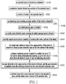
- FIG. 1 is a flowchart illustrating a manufacturing method of a trench power semiconductor device according to an embodiment of the present disclosure
- FIGS. 2A-2O are respectively partial sectional views illustrating the trench power semiconductor device at each step of the manufacturing method according to an embodiment of the present disclosure.
- FIGS. 3A-3C are respectively partial sectional views illustrating the trench power semiconductor device at each step of the manufacturing method according to another embodiment of the present disclosure.
- FIG. 1 is a flowchart illustrating a manufacturing method of a trench power semiconductor device according to an embodiment of the present disclosure.
- FIGS. 2A-2O are partial sectional views illustrating trench power semiconductor device at each step of the manufacturing method according to an embodiment of the present disclosure.
- step S 100 an epitaxial layer is formed on a substrate and, and in step S 200 , a protective layer is formed on a surface of the epitaxial layer.
- FIGS. 2A-2B are referred to collectively in the following description.
- the epitaxial layer 11 is formed on the substrate 10 , and the epitaxial layer 11 has a surface 11 s away from the substrate 10 .
- the substrate 10 is heavily doped with first type conductive dopants to serve as a drain of the trench power semiconductor device.
- the first type conductive dopants can be N-type or P-type conductive dopants.
- the N-type conductive dopants are pentavalent element ions such as phosphorous ions or arsenic ions
- the P-type conductive dopants are trivalent element ions such as boron ions, aluminum ions or gallium ions.
- the epitaxial layer 11 is of the same conductive type as the substrate 10 but is with less doping concentration than the substrate 10 .
- the substrate 10 has a high concentration of N-type dopant (N + doping), but the epitaxial layer 11 has a low concentration of N-type dopant (N ⁇ doping).
- the substrate 10 has high concentration of P-type dopant (P + doping) but the epitaxial layer 11 has low concentration of P-type dopant (P ⁇ doping).
- a pad oxide 12 is formed on the surface 11 s of the epitaxial layer 11 .
- the pad oxide 12 can serve as an etching stopping layer in the subsequent manufacturing process.
- a protective layer 13 is formed on the pad oxide 12 .
- the material of the protective layer 13 is different from the pad oxide 12 .
- the material for the protective layer 13 can be nitride oxide, such as silicon nitride, which is capable of protecting the surface 11 s of the protective layer from oxidation in the following thermal oxidation process.
- the manufacturing method of the trench power semiconductor device of the present embodiment further includes forming a hard film layer 14 on the protective layer 13 .
- a trench is formed in the epitaxial layer.
- a trench 11 h is formed in the epitaxial layer 11 .
- an opening hl in spatial connection with the trench 11 h is also formed in the hard film layer 14 and the protective layer 13 .
- the step of forming the trench 11 h and the opening hl can be implemented by known techniques. For example, a pattern photoresist (not shown in the figure) is firstly formed on the hard film layer 14 so that a position of the opening hl can be defined. After that, the opening hl is formed through the pattern photoresist, and then the trench 11 h is further formed in the epitaxial layer 11 . Furthermore, the trench 11 h can be formed in the epitaxial layer 11 by an etching process such as dry etching or wet etching.
- a sacrificial oxide layer SAC should first be formed on the inner sidewall of the trench 11 h and then removed, which allows the inner sidewall of the trench 11 h to be repaired.
- the crystallographic defect on the inner sidewall can thereby be reduced to prevent electrical leakage.
- the surface of the epitaxial layer 11 has the protective layer 13 and the hard film layer 14 . Therefore, the surface 11 s of the epitaxial can be protected from oxidation during the forming of the sacrificial oxide layer SAC through the thermal oxidation process.
- the sacrificial oxide layer SAC is then removed.
- step S 400 a trench gate structure is formed in the trench.
- the step of forming the gate structure further includes steps S 401 to S 407 .
- step S 401 an insulating layer covering an inner surface of the trench is formed.
- the insulating layer 15 covers the inner surface of the trench 11 h , and has an outline substantially the same as the inner surface of the trench 11 h .
- the insulating layer 15 has two opposite inner sidewalls 15 a and a bottom end portion 15 b connecting with the two inner sidewalls 15 a .
- the insulating layer 15 can be an oxide layer formed by the thermal oxidation process, such as silicon oxide.
- step S 402 an initial spacing layer is formed. A more detailed description will be provided in FIGS. 2H-2I .
- a spacing dielectric layer 16 ′′ is formed.
- the spacing dielectric layer 16 ′′ covers the surface of the hard film layer 14 , the inner surface of the opening hl, the two sidewalls 15 a and the bottom end portion 15 b of the insulating layer 15 , in a carpet-like manner.
- the material of the spacing dielectric layer 16 ′′ can be the same as the material of the protective layer 13 , such as nitride.
- the material of the spacing dielectric layer 16 ′′ is different from that of the insulation layer 15 .
- the thickness of the spacing dielectric layer 16 ′′ is kept substantially the same, that is to say, the thickness is not decreased with the increase of the depth of the trench 11 h.
- FIG. 2I The bottom end portion 15 b of the insulation layer 15 and the spacing dielectric layer 16 ′′ covering the hard film layer 14 are removed to form the initial spacing layer 16 ′.
- dry etching is used to remove the bottom end portion 15 b of the insulation layer 15 and the spacing dielectric layer 16 ′′ covering the hard film layer 14 , leaving the spacing dielectric layer on the two inner sidewalls 15 a of the insulation layer 15 (i.e., the initial spacing layer 16 ′).
- the initial spacing layer 16 ′ has a first sidewall portion 161 ′ and a second sidewall portion 162 ′ respectively covering the two inner sidewalls 15 a .
- the bottom of the first sidewall portion 161 ′ is separate from the bottom of the second sidewall portion 162 ′, so as to be exposed from the bottom end portion 15 b of the insulating layer 15 .
- the first sidewall portion 161 ′ and the second sidewall portion 162 ′ both have a extending portion 161 'S, 162 'S protruding from the protective layer 13 , and the extending portions 161 'S, 162 'S cover the inner surface of the opening hl.
- step S 403 an initial inner dielectric layer covering the initial spacing layer is formed, in which the bottom of the initial inner dielectric layer is directly in contact with the bottom end portion of the insulating layer 15 .
- the initial inner dielectric layer 17 ′ covers on the surface 11 s of the epitaxial layer 11 and in the trench 11 h . Moreover, the bottom of the initial inner dielectric layer 17 ′ is directly in contact with the bottom end portion 15 b of the insulating layer 15 . In the present embodiment, the material of the initial inner dielectric layer 17 ′ is different from that of the initial spacing layer 16 ′, but is the same as that of the insulating layer 15 . In one embodiment, the insulating layer 15 and the initial inner dielectric layer 17 ′ are both silicon oxide layers, and the initial spacing layer 16 ′ is a silicon nitride layer.
- the materials filled into the bottom of the trench 11 h is more pure, so that the electric field distribution at the bottom of the trench can be alleviated, and that the avalanche voltage of the devices can be increased without sacrificing the on-resistance.
- step S 404 a heavily-doped semiconductor material is formed at the lower portion of the trench.
- step S 405 the initial inner dielectric layer at the upper portion of the trench is removed to form an inner dielectric layer at the low portion of the trench.
- the heavily-doped semiconductor material 18 ′ is filled into the lower portion of the trench 11 h.
- a heavily-doped semiconductor layer is formed on the epitaxial layer 11 , and then filled in the trench 11 h . After that, the heavily-doped semiconductor layer covering the epitaxial layer 11 is etched back, leaving the heavily-doped semiconductor material 18 ′ at the lower portion of the trench 12 .
- the heavily-doped semiconductor material 18 ′ can be such as doped poly-Si.
- the top of the heavily-doped semiconductor material 18 ′ protrudes out of the top of the inner dielectric layer 17 .
- the hard film layer 14 on the protective layer 13 is also removed.
- step S 406 a thermal oxidation process is applied to oxidize the top of the heavily-doped semiconductor material, so as to form the inter-electrode dielectric layer 19 and the shielding electrode 18 .
- the top of the heavily-doped semiconductor material 18 ′ is oxidized, forming the inter-electrode dielectric layer 19 .
- the portion of the heavily-doped semiconductor material 18 ′ not being oxidized forms the shielding electrode 18 . It should be noted that due to the protection of the initial spacing layer 16 ′ and the protective layer 13 , the epitaxial layer 11 is not oxidized during the thermal oxidation process.
- step S 407 the gate electrode at the upper portion of the trench is formed.
- the gate electrode is insulated from the shielding electrode by the inter-electrode dielectric layer.
- FIGS. 2M to 2N Reference is made to FIGS. 2M to 2N .
- the extending portions 161 'S, 162 'S and the initial spacing layer 16 ′ at the upper portion of the trench 11 h will be firstly removed to form a spacing layer 16 .
- the protective layer 13 will also be removed in this step.
- the spacing layer 16 is located below the gate electrode 20 , and includes a first spacing portion 161 and a second spacing portion 162 respectively at the two opposite sides of the shielding electrode 18 .
- the insulating layer 15 , the inter-electrode dielectric layer 19 and the spacing layer 16 define an accommodation space H 1 on the upper portion of the trench 11 h .
- the gate electrode 20 is formed in the accommodation space H 1 on the upper portion of the trench 11 h.
- doped poly-Si can be firstly formed and carpeted on the epitaxial layer 11 and filled in the accommodation space H 1 , and the doped poly-Si on the epitaxial layer 11 can then be etched back to form the gate electrode 20 .
- the trench gate structure G 1 can be formed in the trench 11 h.
- step S 500 a substrate area and a source area are formed in the epitaxial layer.
- the source area is on top of the substrate area.
- a step of forming a wire redistribution layer on the surface of the epitaxial layer is further included.
- FIG. 2O in which the sectional view of the trench power semiconductor device according to the embodiment of the present disclosure is illustrated.
- a substrate doping process is performed on the epitaxial layer 11 to form a low doping area, and the low doping area has an opposite conductive type to the epitaxial layer 11 .
- a source doping manufacturing is performed on the light doping area to form a high doping area at the upper portion of the light doping area, and the conductive type of the high doping area is opposite to that of the low doping area.
- a drive-in manufacturing is next performed to allow the diffusion of the dopants in the low and high doping areas to form the substrate area 110 and the source area 111 .
- the source area 111 is on top of the substrate area 110 .
- the wire redistribution layer can then be formed on the epitaxial layer 11 , so as to allow the source area 111 , the gate electrode 20 and the shielding electrode 18 to be electrically connected with an external control circuit.
- the forming of the wire redistribution layer can be implemented by known techniques.
- an interlayer dielectric layer 21 is formed on the epitaxial layer 11 first. After that, a plurality of contact windows 21 h penetrating the interlayer dielectric layer 21 are then formed, and the plurality of contact windows 21 h extend to the source area 111 .
- a doping process is performed through the contact windows 21 h to form a heavily-doped contact area 112 under the contact windows 21 h .
- a conductive pillar 22 is formed in the contact window 21 h , and a source metal layer 23 connecting with the conductive pillar 22 is formed on the interlayer dielectric layer 21 . That is to say, the source metal layer 23 can, through the conductive pillar 22 , electrically connect with the source area 111 .
- the trench gate structure G 1 of the trench power semiconductor device T 1 manufactured by the above process includes the insulating layer 15 , the spacing layer 16 , the inner dielectric layer 17 , the shielding electrode 18 , the inter-electrode dielectric layer 19 and the gate electrode 20 .
- the material of the spacing layer 16 is different from that of the insulating layer 15 and the inner dielectric layer 17 .
- the spacing layer 16 includes the first spacing portion 161 and the second spacing portion 162 .
- the bottom of the first spacing portion 161 is spaced apart from the bottom of the second spacing portion 162 at a predetermined distance, and the predetermined distance is greater than the width of the shielding electrode 18 .
- the first and the second spacing portions 161 , 162 are at the lower portion of the trench 11 h , and is interveningly disposed between the insulating layer 15 , the inter-electrode dielectric layer 19 and the inner dielectric layer 17 . That is to say, the first spacing portion 161 and the second spacing portion 162 do not serve as the gate insulating layer.
- FIGS. 3A-3C where 3 A- 3 C are respectively partial sectional views illustrating trench power semiconductor device at each step of the manufacturing method according to another embodiment of the present disclosure.
- the first spacing portion 161 and the second spacing portion 162 of the trench power semiconductor device T 2 manufactured by the present embodiment cooperate with the insulating layer 15 to serve as the gate insulating layer.
- the steps in FIGS. 3A-3C are performed after the steps in FIGS. 2A-2L .
- the gate electrode 20 of FIG. 3A is formed in the upper portion of the trench 11 h without removing the extending portions 161 'S, 162 'S, the protective layer 13 and the initial spacing layer 16 ′ at the upper portion of the trench 11 h.
- the protective layer 13 and the extending portions 161 'S, 162 'S on the epitaxial layer 11 is then removed to form the spacing layer 16 .
- the protective layer 13 and the extending portions 161 'S, 162 'S can be removed by chemical mechanical polishing or selective etching.
- first spacing portion 161 and the second spacing portion 162 both extend from the upper portion of the trench 11 h to the lower portion of the trench 11 h .
- first spacing portion 161 and the second spacing portion 162 cooperate with the insulating layer 15 to serve as the gate insulating layer to adjust the work function between the substrate area 110 and the gate electrode 20 , so as to decrease the leakage current when operating under reverse bias.
- the substrate area 110 , the source area 111 and the wire redistribution layer are then formed, as shown by the trench power semiconductor device T 2 in FIG. 3C .
- the spacing layer 16 is formed on the surface 11 s of the epitaxial layer 11 and the sidewall of the trench 11 h before the forming of the inter-electrode dielectric layer 19 by thermal oxidation process, so as to protect the surface 11 s of the epitaxial layer 11 and the sidewall of the trench 11 h from oxidation.
- the bottom of the first spacing portion 161 is separate from the bottom of the second spacing portion 162 , that is, when a reverse bias is applied to the trench power semiconductor device, since the materials filled into the bottom of the trench 11 h and right under the shielding electrode 18 are more pure, the electric field distribution at the bottom of the trench 11 h can be alleviated. That is, the avalanche voltage of the devices can be increased without sacrificing the on-resistance.
- the doping concentration of the epitaxial layer 11 can further be optimized to reduce the on-resistance, so as to increase the voltage conversion efficiency of the trench power semiconductor device.
- the bottom of the trench 11 h of the trench power semiconductor device exhibits a gentle electric field, which increases the avalanche voltage. Therefore, the trench power semiconductor device according to the embodiments of the present disclosure exhibits a 50% decrease for the on-resistance.
- the work function between the substrate area 110 and the gate electrode 20 can be adjusted, so as to decrease the leakage current when the trench power semiconductor device T 2 is operated under reverse bias.
- the manufacturing method of the trench power semiconductor device according to the embodiments of the present disclosure can be integrated into current semiconductor manufacturing processes to provide the trench power semiconductor device of the present disclosure.
Landscapes
- Electrodes Of Semiconductors (AREA)
Abstract
Description
Claims (14)
Applications Claiming Priority (2)
| Application Number | Priority Date | Filing Date | Title |
|---|---|---|---|
| TW106122021 | 2017-06-30 | ||
| TW106122021A TWI622124B (en) | 2017-06-30 | 2017-06-30 | Method for manufacturing trench type power semiconductor device |
Publications (2)
| Publication Number | Publication Date |
|---|---|
| US20190006489A1 US20190006489A1 (en) | 2019-01-03 |
| US10559674B2 true US10559674B2 (en) | 2020-02-11 |
Family
ID=62639992
Family Applications (1)
| Application Number | Title | Priority Date | Filing Date |
|---|---|---|---|
| US15/988,018 Active 2038-05-25 US10559674B2 (en) | 2017-06-30 | 2018-05-24 | Manufacturing method of a trench power semiconductor device |
Country Status (2)
| Country | Link |
|---|---|
| US (1) | US10559674B2 (en) |
| TW (1) | TWI622124B (en) |
Families Citing this family (6)
| Publication number | Priority date | Publication date | Assignee | Title |
|---|---|---|---|---|
| TWI704606B (en) * | 2019-04-24 | 2020-09-11 | 帥群微電子股份有限公司 | Trench power semiconductor device and manufacturing method thereof |
| TWI754367B (en) | 2020-09-01 | 2022-02-01 | 富鼎先進電子股份有限公司 | Method for manufacturing trench type semiconductor device |
| CN114121628B (en) * | 2020-09-01 | 2025-03-25 | 富鼎先进电子股份有限公司 | Method for manufacturing trench semiconductor device |
| JP7414677B2 (en) * | 2020-09-15 | 2024-01-16 | 株式会社東芝 | Semiconductor device and its manufacturing method |
| TWI809577B (en) * | 2021-11-26 | 2023-07-21 | 帥群微電子股份有限公司 | Trench power semiconductor device and method of manufacturing the same |
| CN114582965B (en) * | 2022-05-06 | 2022-07-19 | 南京微盟电子有限公司 | A low switching loss power device structure and its manufacturing method |
Citations (1)
| Publication number | Priority date | Publication date | Assignee | Title |
|---|---|---|---|---|
| US20120276703A1 (en) * | 2009-12-09 | 2012-11-01 | Semiconductor Components Industries, Llc | Method of forming an insulated gate field effect transistor device having a shield electrode structure |
Family Cites Families (6)
| Publication number | Priority date | Publication date | Assignee | Title |
|---|---|---|---|---|
| US7345342B2 (en) * | 2001-01-30 | 2008-03-18 | Fairchild Semiconductor Corporation | Power semiconductor devices and methods of manufacture |
| US7091573B2 (en) * | 2002-03-19 | 2006-08-15 | Infineon Technologies Ag | Power transistor |
| TWI256676B (en) * | 2004-03-26 | 2006-06-11 | Siliconix Inc | Termination for trench MIS device having implanted drain-drift region |
| US7633119B2 (en) * | 2006-02-17 | 2009-12-15 | Alpha & Omega Semiconductor, Ltd | Shielded gate trench (SGT) MOSFET devices and manufacturing processes |
| TWI567931B (en) * | 2014-12-05 | 2017-01-21 | 帥群微電子股份有限公司 | Semiconductor component and method of manufacturing same |
| TWI570917B (en) * | 2014-12-31 | 2017-02-11 | 帥群微電子股份有限公司 | Trench type power MOS half field effect transistor and manufacturing method thereof |
-
2017
- 2017-06-30 TW TW106122021A patent/TWI622124B/en active
-
2018
- 2018-05-24 US US15/988,018 patent/US10559674B2/en active Active
Patent Citations (1)
| Publication number | Priority date | Publication date | Assignee | Title |
|---|---|---|---|---|
| US20120276703A1 (en) * | 2009-12-09 | 2012-11-01 | Semiconductor Components Industries, Llc | Method of forming an insulated gate field effect transistor device having a shield electrode structure |
Also Published As
| Publication number | Publication date |
|---|---|
| TW201906078A (en) | 2019-02-01 |
| TWI622124B (en) | 2018-04-21 |
| US20190006489A1 (en) | 2019-01-03 |
Similar Documents
| Publication | Publication Date | Title |
|---|---|---|
| US10559674B2 (en) | Manufacturing method of a trench power semiconductor device | |
| US10566422B2 (en) | Power semiconductor device and method for manufacturing the same | |
| TWI470790B (en) | Ditch-type gate MOS half-field effect transistor | |
| US8772865B2 (en) | MOS transistor structure | |
| US8304314B2 (en) | Method of forming an MOS transistor | |
| US9368621B1 (en) | Power semiconductor device having low on-state resistance | |
| US10529847B2 (en) | Trench power semiconductor component and method of manufacturing the same | |
| KR20190087786A (en) | Semiconductor device and method of manufacturing the same | |
| US9991378B2 (en) | Trench power semiconductor device | |
| TW201351651A (en) | Semiconductor device and method of manufacturing same | |
| CN112713192A (en) | Shielded gate trench MOSFET device with electrostatic protection capability and manufacturing method thereof | |
| US10153274B2 (en) | Semiconductor device | |
| US11244830B2 (en) | Semiconductor device and manufacturing method thereof | |
| US8933512B2 (en) | MOSFET and method for manufacturing the same | |
| US9299616B1 (en) | Integrated circuits with separate workfunction material layers and methods for fabricating the same | |
| CN109585547B (en) | Trench type power semiconductor element and manufacturing method thereof | |
| KR102472673B1 (en) | Semiconductor device and method for manufacturing the same | |
| US20240274712A1 (en) | Field-effect transistors with self-aligned p-shield contacts | |
| TWI546956B (en) | Trench gate mosfet | |
| CN111162124B (en) | Semiconductor structures and methods of forming them | |
| CN107978599B (en) | Semiconductor structure, method of forming the same, and method of measuring capacitance | |
| CN114068701A (en) | Semiconductor structure and forming method thereof | |
| CN109216450B (en) | Manufacturing method of trench type power semiconductor element | |
| CN113437148B (en) | Semiconductor structures and methods of forming them | |
| US9748333B2 (en) | Semiconductor structure including dummy structure and semiconductor pattern structure including dummy structure |
Legal Events
| Date | Code | Title | Description |
|---|---|---|---|
| AS | Assignment |
Owner name: SUPER GROUP SEMICONDUCTOR CO., LTD., TAIWAN Free format text: ASSIGNMENT OF ASSIGNORS INTEREST;ASSIGNORS:HSU, HSIU-WEN;YEH, CHUN-YING;NI, CHUN-WEI;AND OTHERS;REEL/FRAME:046227/0859 Effective date: 20180518 |
|
| FEPP | Fee payment procedure |
Free format text: ENTITY STATUS SET TO UNDISCOUNTED (ORIGINAL EVENT CODE: BIG.); ENTITY STATUS OF PATENT OWNER: SMALL ENTITY |
|
| FEPP | Fee payment procedure |
Free format text: ENTITY STATUS SET TO SMALL (ORIGINAL EVENT CODE: SMAL); ENTITY STATUS OF PATENT OWNER: SMALL ENTITY |
|
| STPP | Information on status: patent application and granting procedure in general |
Free format text: DOCKETED NEW CASE - READY FOR EXAMINATION |
|
| STPP | Information on status: patent application and granting procedure in general |
Free format text: NON FINAL ACTION MAILED |
|
| STPP | Information on status: patent application and granting procedure in general |
Free format text: RESPONSE TO NON-FINAL OFFICE ACTION ENTERED AND FORWARDED TO EXAMINER |
|
| STPP | Information on status: patent application and granting procedure in general |
Free format text: NOTICE OF ALLOWANCE MAILED -- APPLICATION RECEIVED IN OFFICE OF PUBLICATIONS |
|
| STPP | Information on status: patent application and granting procedure in general |
Free format text: PUBLICATIONS -- ISSUE FEE PAYMENT VERIFIED |
|
| STCF | Information on status: patent grant |
Free format text: PATENTED CASE |
|
| MAFP | Maintenance fee payment |
Free format text: PAYMENT OF MAINTENANCE FEE, 4TH YR, SMALL ENTITY (ORIGINAL EVENT CODE: M2551); ENTITY STATUS OF PATENT OWNER: SMALL ENTITY Year of fee payment: 4 |