US10559575B2 - Non-volatile memory with restricted dimensions - Google Patents
Non-volatile memory with restricted dimensions Download PDFInfo
- Publication number
- US10559575B2 US10559575B2 US16/057,193 US201816057193A US10559575B2 US 10559575 B2 US10559575 B2 US 10559575B2 US 201816057193 A US201816057193 A US 201816057193A US 10559575 B2 US10559575 B2 US 10559575B2
- Authority
- US
- United States
- Prior art keywords
- memory
- control gate
- gate selection
- semiconductor
- recesses
- Prior art date
- Legal status (The legal status is an assumption and is not a legal conclusion. Google has not performed a legal analysis and makes no representation as to the accuracy of the status listed.)
- Active
Links
Images


Classifications
-
- H—ELECTRICITY
- H10—SEMICONDUCTOR DEVICES; ELECTRIC SOLID-STATE DEVICES NOT OTHERWISE PROVIDED FOR
- H10B—ELECTRONIC MEMORY DEVICES
- H10B41/00—Electrically erasable-and-programmable ROM [EEPROM] devices comprising floating gates
- H10B41/40—Electrically erasable-and-programmable ROM [EEPROM] devices comprising floating gates characterised by the peripheral circuit region
-
- H01L27/11526—
-
- G—PHYSICS
- G11—INFORMATION STORAGE
- G11C—STATIC STORES
- G11C16/00—Erasable programmable read-only memories
- G11C16/02—Erasable programmable read-only memories electrically programmable
-
- G—PHYSICS
- G11—INFORMATION STORAGE
- G11C—STATIC STORES
- G11C16/00—Erasable programmable read-only memories
- G11C16/02—Erasable programmable read-only memories electrically programmable
- G11C16/04—Erasable programmable read-only memories electrically programmable using variable threshold transistors, e.g. FAMOS
- G11C16/0408—Erasable programmable read-only memories electrically programmable using variable threshold transistors, e.g. FAMOS comprising cells containing floating gate transistors
- G11C16/0433—Erasable programmable read-only memories electrically programmable using variable threshold transistors, e.g. FAMOS comprising cells containing floating gate transistors comprising cells containing a single floating gate transistor and one or more separate select transistors
-
- G—PHYSICS
- G11—INFORMATION STORAGE
- G11C—STATIC STORES
- G11C16/00—Erasable programmable read-only memories
- G11C16/02—Erasable programmable read-only memories electrically programmable
- G11C16/06—Auxiliary circuits, e.g. for writing into memory
-
- G—PHYSICS
- G11—INFORMATION STORAGE
- G11C—STATIC STORES
- G11C16/00—Erasable programmable read-only memories
- G11C16/02—Erasable programmable read-only memories electrically programmable
- G11C16/06—Auxiliary circuits, e.g. for writing into memory
- G11C16/10—Programming or data input circuits
- G11C16/14—Circuits for erasing electrically, e.g. erase voltage switching circuits
-
- G—PHYSICS
- G11—INFORMATION STORAGE
- G11C—STATIC STORES
- G11C5/00—Details of stores covered by group G11C11/00
- G11C5/02—Disposition of storage elements, e.g. in the form of a matrix array
- G11C5/025—Geometric lay-out considerations of storage- and peripheral-blocks in a semiconductor storage device
-
- H01L27/11524—
-
- H01L27/11529—
-
- H—ELECTRICITY
- H10—SEMICONDUCTOR DEVICES; ELECTRIC SOLID-STATE DEVICES NOT OTHERWISE PROVIDED FOR
- H10B—ELECTRONIC MEMORY DEVICES
- H10B41/00—Electrically erasable-and-programmable ROM [EEPROM] devices comprising floating gates
- H10B41/30—Electrically erasable-and-programmable ROM [EEPROM] devices comprising floating gates characterised by the memory core region
- H10B41/35—Electrically erasable-and-programmable ROM [EEPROM] devices comprising floating gates characterised by the memory core region with a cell select transistor, e.g. NAND
-
- H—ELECTRICITY
- H10—SEMICONDUCTOR DEVICES; ELECTRIC SOLID-STATE DEVICES NOT OTHERWISE PROVIDED FOR
- H10B—ELECTRONIC MEMORY DEVICES
- H10B41/00—Electrically erasable-and-programmable ROM [EEPROM] devices comprising floating gates
- H10B41/40—Electrically erasable-and-programmable ROM [EEPROM] devices comprising floating gates characterised by the peripheral circuit region
- H10B41/41—Electrically erasable-and-programmable ROM [EEPROM] devices comprising floating gates characterised by the peripheral circuit region of a memory region comprising a cell select transistor, e.g. NAND
Definitions
- Embodiments relate to memories, especially non-volatile memories, and in particular embodiments to non-volatile memory with restricted (e.g. compact) dimensions.
- a memory cell Customarily in EEPROM memory devices, a memory cell includes a state transistor intended to store an item of information.
- the state transistor includes a control gate and a floating gate, in series with an access transistor, or bit line selection transistor.
- the access transistor is controlled by a word line signal and makes it possible to access the state transistor electrically, in particular in order to read an item of data therefrom or write an item of data thereto.
- Control gate selection transistors are connected between gate control lines and the control gates of the state transistors of a memory word.
- the control gate selection transistors are controlled by a dedicated control signal and make it possible to access the memory cells electrically, in particular in order to read an item of data therefrom or write an item of data thereto.
- the voltages implemented in the course of data writes must be high enough to inject or extract a charge of the floating gate of the state transistors through the Fowler-Nordheim effect.
- the access transistors and control gate selection transistors intrinsically exhibit voltage limits beyond which they risk breakdowns, such as avalanches of the source-substrate or drain-substrate junctions, and premature wear.
- a memory word includes in a customary manner a group of memory cells, for example an octet or byte.
- control gate selection transistor having a breakdown voltage of its source-substrate or drain-substrate junction of the order of 12V.
- high programming voltages of 14V to 15V are transmitted to the state transistor of a memory cell via the access transistor.
- the access transistors have a breakdown voltage of their source-substrate or drain-substrate junctions of the order of 12V.
- the split voltage solution involves, briefly, applying combinations of negative and positive potentials so as to reach the high voltages required without however exceeding the breakdown voltages of the components.
- the split voltage technologies require in particular two charge pumps (one generating a negative potential and the other a positive potential), each using a substantial and relatively significant surface area at the periphery of the memory plane of the memory.
- the split voltage solution may be unsuitable, for example for low-density memories, comprising an already small memory plane which therefore cannot accept a large surface area at the periphery.
- a device includes electrically conducting tracks coupling each control gate selection transistor to control gates of state transistors of a memory word to which it is allocated, each conducting track passing above at least one control gate selection transistor produced in a recess housing the memory word.
- the succession of recesses includes an alternation of first recesses and of second recesses, the first recesses being electrically mutually coupled and the second recesses being electrically mutually coupled.
- the memory words are arranged in rows and columns in the memory plane, half the memory words of one and the same row forming an even page and the other half of the memory words of this row forming an odd page, in which the even pages are produced in the first recesses and the odd pages are produced in the second recesses, the memory being accessible page-wise.
- the device includes an erasure circuit configured to erase the memory cells of a selected memory word by applying an erasure voltage on the control gates of the state transistors of the memory cells of the selected memory word, via the conduction terminals of the control gate selection transistor allocated to the selected memory word, and by applying, in the recess containing the control gate selection transistor, a first compensation voltage adapted to prevent junction breakdown between the control gate selection transistor and the recess which contains it.
- the erasure circuit is configured to apply the high erasure voltage equal to substantially 15 volts and the first compensation voltage equal to substantially 3 volts.
- each memory cell includes an access transistor coupled in series with the state transistor of the memory cell
- the device includes a programming circuit configured to program a selected memory cell belonging to a selected memory word, by applying a programming voltage to the conduction terminals of the access transistor of the selected memory cell, and by applying, in the recess containing the selected memory word, a second compensation voltage adapted to prevent junction breakdown between the access transistor and the recess which contains it.
- the programming circuit is configured to apply the high programming voltage equal to substantially 15 volts and the second compensation voltage equal to substantially 3 volts.
- FIGS. 1 to 6 illustrate examples of embodiments and of modes of implementation of the invention.
- a memory device of the electrically erasable and programmable non-volatile memory type, including a memory plane including a succession of electrically mutually insulated neighbor semiconductor recesses of a first type of conductivity, each recess housing memory words possessing memory cells, each including a state transistor having a floating gate and a control gate, and respective control gate selection transistors allocated to each memory word, each control gate selection transistor being coupled to the control gates of the state transistors of the memory word to which it is allocated, each control gate selection transistor being situated in and on a neighbor semiconductor recess of the semiconductor recess housing the memory word to which it is allocated.
- the proposed device is compatible with the split voltage techniques.
- the device includes semiconductor wells of a second type of conductivity opposite to the first type of conductivity and configured to laterally insulate two neighbor recesses and a semiconductor buried layer of the second type of conductivity configured to vertically insulate each recess from the remainder of a semiconductor subjacent substrate of the first type of conductivity.
- FIG. 1 represents a part of a memory plane PM of a non-volatile memory of the electrically erasable and programmable type EE formed in and on a semiconductor substrate of a first type of conductivity.
- the memory plane PM includes memory cells CEL, each including an access transistor TA and a state transistor TE having a floating gate and a control gate.
- the memory cells are grouped into memory words WD, each memory word WD including, for example, eight memory cells.
- Each memory word WD belongs to a column COL and to a row RG organizing the memory plane PM in matrix fashion.
- the columns follow one another in a first direction X of the memory plane PM and the rows follow one another in a second direction Y of the memory plane PM.
- a row can include an even page and an odd page.
- a page represents for example the largest quantity of data that can be written by the memory in a single write cycle.
- the memory is then said to be accessible page-wise.
- a memory cell is accessible via respective bit lines BL (shown as BL 0 -BL 15 in FIG. 1 ), each being coupled to the drain of the access transistor TA of the respective cell.
- the access transistors TA are controlled on their gates by a word line signal applied to a word line WL which is common to all the memory cells CEL of one and the same row RG.
- the state transistors TE are for their part controlled by a control signal CG applied to their control gates.
- the control signal CG is applied to the control gates of all the state transistors of a memory word via the conduction terminals of a control gate selection transistor CGT allocated to each memory word WD.
- control gate selection transistors CGT of one and the same row are controlled on their gates by one and the same signal dedicated to the control gate selection transistors and transmitted by a control line CGL.
- the sources of the state transistors TE are linked to a source line SL, common to all the memory cells situated in one and the same recess of the memory plane PM.
- the first recess B 0 of the first type of conductivity for example type P (otherwise referred to as p-type)
- the second recess B 1 is also of the first type of conductivity.
- first recess B 0 and the second recess B 1 are electrically insulated from one another and from the remainder of the substrate, by a single semiconductor well of a second type of conductivity opposite to the first type of conductivity, for example type N (otherwise referred to as n-type).
- first recesses B 0 and of second recesses B 1 of the same type of conductivity in the succession of recesses allows optimization of the quantity of surface area occupied by the control and decoding elements (not represented in the figures) situated at the periphery of the memory plane.
- the control gate selection transistors CGT allocated to the memory words WD produced in and on the first recess B 0 are produced in and on the second recess B 1 .
- the control gate selection transistors CGT allocated to the memory words WD produced in and on the second recess B 1 are produced in and on the first recess B 0 .
- the memory plane includes a succession of numerous first recesses B 0 and second recesses B 1 which are neighbors in alternation. All the first recesses B 0 are electrically coupled; likewise, all the second recesses B 1 are electrically coupled.
- Each control gate selection transistor CGT allocated to the memory words produced in the first recesses B 0 is produced in one of the two second recesses B 1 which are neighbors of the respective first recess B 0 ; likewise, each control gate selection transistor CGT allocated to the memory words produced in the second recesses B 1 is produced in one of the two first recesses B 0 which are neighbors of the respective second recess B 1 .
- the memory includes a memory plane PM includes a succession of semiconductor recesses of a first type of conductivity B 0 , B 1 which are neighbors and electrically insulated from one another.
- Each recess B 0 , B 1 houses memory words WD, and control gate selection transistors CGT respectively allocated to each memory word WD, each control gate selection transistor CGT being coupled to the control gates of the state transistors TE of the memory word to which it is allocated, the control gate selection transistors CGT being situated in and on a neighbor semiconductor recess B 1 , B 0 of the semiconductor recess B 0 , B 1 housing the memory word WD to which it is allocated.
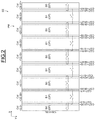
- FIG. 2 represents an exemplary memory plane PM of a 64K non-volatile memory EE of the type of that described above.
- the memory plane PM includes, in this example, four first recesses B 0 , considering that the two half-recesses situated at the lateral ends (along the first direction X, that is to say, in the figure, at the left and right ends of the memory plane) form a single recess.
- the memory plane PM also includes, in this example, four first recesses B 1 .
- the succession of recesses includes an alternation of first recesses B 0 and of second recesses B 1 , the first recesses B 0 being electrically mutually coupled and the second recesses B 1 being electrically mutually coupled.
- each first recess B 0 is a neighbor in the memory plane PM of two second recesses B 1 and each second recess B 1 is a neighbor in the memory plane PM of two first recesses B 0 (except for the recesses situated at the ends of the memory plane PM).
- This organization makes it possible to dispose half the pages, the so-called even pages EP, in a manner interleaved with the other half of the pages, the so-called odd pages OP, in the hardware disposition of the memory plane.
- the parity of the pages is considered in the sense of their logical organization, termed the “arrangement in the memory plane”, in particular in that they are always consecutive to one another in the arrangement of the memory plane (that is to say that the page following or preceding an even page is an odd page, and the page following or preceding an odd page is an even page).
- each recess includes 8 memory words WD and therefore according to an arrangement in the memory plane PM of 8 columns per recess.
- columns Col 0 to Col 31 (i.e. Col ⁇ 0 : 3 >, Col ⁇ 4 : 11 >, Col ⁇ 12 : 19 >, Col ⁇ 20 : 27 >, Col ⁇ 28 : 31 >) are formed in the first recesses B 0 , the intersection of a row WL with these 32 consecutive columns forms an even page EP.
- columns Col 32 to Col 63 are formed in the second recesses B 1 , the intersection of a row WL with these 32 consecutive columns forms an odd page OP.
- the memory plane is thus arranged according to 64 columns (Col ⁇ 0 : 63 >) and 128 rows (WL).
- Four additional rows are furthermore disposed on the edges (in the second direction Y) of the memory plane PM but are electrically unused. These “dummy” additional rows make it possible to avoid undesirable edge effects in the electrically active rows.
- This criss-cross organization of the even pages EP and of the odd pages OP makes it possible to halve the number of physical rows of the memory plane PM (in the second direction Y), by disposing them in a criss-cross fashion in the arrangement of the columns (in the first direction X).
- the size of the row decoder is halved, and on the other hand, the size of the column decoder is also reduced along the second direction Y.
- the column decoder essentially including bit line latches and making it possible to access each bit line, is advantageously demultiplexed towards the columns of the even rows or towards the columns of the odd rows.
- This organization offering twice as much space in the first direction X to dispose as many bit line latches, makes it possible to correspondingly reduce the footprint of the decoder of columns in the second direction Y.
- the footprint of the demultiplexing circuit is moreover regarded as negligible with respect to the column decoder.
- a memory device EE in which the memory words WD are arranged in rows and columns in the memory plane PM, the memory words WD of one and the same row forming a page EP, OP, and in which even pages EP are produced in the first recesses B 0 and odd pages OP are produced in the second recesses B 1 , the memory being accessible page-wise.
- writing three entire and consecutive pages comprises an access to a first row WLi and to columns Col 0 to Col 31 in their respective first recesses B 0 , followed by an access to the same first row WLi and to columns Col 31 to Col 63 in their respective second recesses, followed by an access to a second row WLi+1 and to columns Col 0 to Col 31 in their respective first recesses B 0 .
- the control gate selection transistors CGT ⁇ 0 : 3 > and CGT ⁇ 28 : 31 > allocated to the memory words of the columns Col ⁇ 0 : 3 > and Col ⁇ 28 : 31 > of the first recess B 0 are formed in the neighbor second recesses B 1 comprising respectively the columns Col ⁇ 32 : 39 > and Col ⁇ 56 : 63 >;
- the control gate selection transistors CGT ⁇ 4 : 7 > and CGT ⁇ 8 : 11 > allocated to the memory words of the columns Col ⁇ 4 : 11 > of the first recess B 0 are formed in the neighbor second recesses B 1 comprising respectively the columns Col ⁇ 32 : 39 > and Col ⁇ 40 : 47 >;
- the control gate selection transistors CGT ⁇ 12 : 15 > and CGT ⁇ 16 : 19 > allocated to the memory words of the columns Col ⁇ 12 : 19 > of the first recess B 0 are formed in the neighbor second recesses B 1 comprising respectively the columns Col ⁇ 40 : 47 > and Col ⁇ 48 : 55 >;
- the control gate selection transistors CGT ⁇ i:j> are formed on the lateral periphery (along the first direction X) of their respective recess, that is to say as close as possible to the neighbor recess comprising the memory word to which they are allocated.
- FIG. 3 represents a sectional view of the example described previously in conjunction with FIG. 1 .
- the first recess B 0 and the second recess B 1 are of the first type of conductivity, here type P.
- a first recess B 0 and a second recess B 1 are electrically insulated laterally (that is to say along the first direction X) by a single semiconductor well NW of a second type of conductivity opposite to the first type of conductivity, here type N.
- the first recesses B 0 and the second recesses B 1 are furthermore electrically insulated from the remainder of the substrate Psub of the first type of conductivity by a buried semiconductor layer Niso of the second type of conductivity and of lateral semiconductor wells NW.
- the lateral semiconductor wells surround the memory plane PM and are of the same nature as the semiconductor wells NW insulating two neighbor recesses.
- Each control gate selection transistor CGT is electrically coupled to the control gates of the state transistors TE of the memory word WD to which it is allocated by an electrically conducting track M passing above at least one control gate selection transistor CGT produced in the recess housing the memory word WD.
- each control gate selection transistor CGT is situated on the lateral periphery of its respective recess, that is to say between the memory words housed in this recess and the insulating semiconductor well NW.
- FIG. 4 represents a sectional view of the example described previously in conjunction with FIG. 2 .
- control gate selection transistors CGT are, in each recess B 0 , B 1 , grouped together in groups of N control gate selection transistors NCGT and are respectively allocated to N memory words NWD housed in one and the same neighbor recess, with N a whole number, for example 4.
- N-tuple a group of N elements, such as transistors or conducting tracks, is designated by the term “N-tuple”.
- control gate selection transistors NCGT are situated on the lateral periphery of their respective recess, that is to say that they are produced between the memory words of this recess and the insulating semiconductor wells NW.
- the N memory words NWD are advantageously arranged consecutively in the arrangement of the memory plane PM.
- Each N-tuple of electrically conducting tracks coupling respectively the control gate selection transistors CGT of an N-tuple NCGT to the N memory words NWD to which they are respectively allocated, thus pass above the N control gate selection transistors of the N-tuple situated in the neighbor recess.
- the value N is essentially related to the interconnections that have to cross one another.
- FIG. 5 represents two tables EF(EP), PG(EP) of values in volts of the voltages to be applied to the selected or non-selected memory cells of the memory plane PM. These voltage values make it possible to implement in a preferential manner an erasure EF(EP) or a programming EF(EP), in the example of an even page EP of a memory such as described previously in conjunction with FIGS. 1 to 4 .
- the various voltage values advantageously make it possible to apply, in particular, high erasure voltages of 15V to the control gates of the state transistors of the memory cells of a selected memory word, and high programming voltages of 15V to the drain region of a state transistor of a selected memory cell, while complying jointly with a breakdown constraint, a gate voltage constraint, and a non-selected memory cells disturbance constraint.
- the breakdown constraint corresponds to maintaining, in the transistors of the memory plane, a voltage of less than 12V between the source and the recess or between the drain and the recess. This makes it possible to avoid breakdowns of the PN junctions of the transistors.
- the gate voltage constraint corresponds to maintaining, in the transistors of the memory plane, a voltage of less than 12V between the gate and the channel region. This makes it possible to avoid premature wear of the transistors.
- the non-selected memory cells disturbance constraint corresponds to maintaining, in the state transistors of non-selected memory cells, a voltage of less than 3V between the control gate and the source or drain region. This makes it possible to avoid losses of charge of the floating gates during the writing of another memory cell.
- a high erasure voltage CGT of 15V is transmitted via the conduction terminals CG of the control gate selection transistor (e.g. by an erasure circuit), thus in order to comply with the breakdown constraint, a first breakdown compensation voltage of 3V is applied in the second recess B 1 .
- a voltage of 18V is applied to the gates CGL of the control gate selection transistors belonging to the same row, thus, in order to comply with the gate voltage constraint, a gate voltage compensation voltage of 6V is applied in the channel regions of the non-selected control gate selection transistors.
- a high programming voltage BL of 15V is transmitted via the conduction terminals of the state transistor of the cells of the selected bit line (e.g. by a programming circuit), thus in order to comply with the breakdown constraint, a second breakdown compensation voltage of 3V is applied in the first recess B 0 .
- a voltage of 18V is applied to the gates WL of the access transistors belonging to the same row, thus, in order to comply with the gate voltage constraint, a gate voltage compensation voltage of 6V is applied in the channel regions of the other access transistors of the row.
- This disturbance compensation voltage of 3V is transmitted by the respective control gate selection transistors by a voltage of 6V applied to their gates CGL.
- the voltage of 9V of the first source line S 0 during programming corresponds to a precharging making it possible to avoid an undesirable current flow in the cell while programming.
- FIGS. 1 to 4 are compatible with split voltage technologies. Indeed, there may be advantages in making joint use of a split voltage technique in the devices presented and described previously.
- the voltages of 18V may necessitate particular technologies, such as charge pumps or various switching circuitry.
- Generating ⁇ 3V may or may not be simpler than generating 18V, this depends on the technological environment of the integrated circuit integrating the memory EE.
- FIG. 6 represents a non-volatile memory EE such as described previously in conjunction with FIGS. 1 to 5 , including the memory plane PM and writing circuit CMD including an erasure circuit and a programming circuit respectively configured to implement erasures and programmings such as described previously in conjunction with FIG. 5 .
- the memory EE is incorporated into an electronic apparatus APP, such as for example a mobile telephone or a tablet. It will be apparent to the person skilled in the art that the embodiments of a memory such as were detailed previously can be included in any other known product not described here.
- the invention is not limited to these embodiments but embraces all variants thereof, for example, the 64K density of the memory described hereinabove in conjunction with FIG. 2 was given by way of example, in particular since it is appropriate to its representation.
Abstract
Description
Claims (20)
Applications Claiming Priority (2)
| Application Number | Priority Date | Filing Date | Title |
|---|---|---|---|
| FR1757908A FR3070537A1 (en) | 2017-08-28 | 2017-08-28 | NON-VOLATILE MEMORY WITH RESTRICTED SIZE |
| FR1757908 | 2017-08-28 |
Publications (2)
| Publication Number | Publication Date |
|---|---|
| US20190067307A1 US20190067307A1 (en) | 2019-02-28 |
| US10559575B2 true US10559575B2 (en) | 2020-02-11 |
Family
ID=60515527
Family Applications (1)
| Application Number | Title | Priority Date | Filing Date |
|---|---|---|---|
| US16/057,193 Active US10559575B2 (en) | 2017-08-28 | 2018-08-07 | Non-volatile memory with restricted dimensions |
Country Status (3)
| Country | Link |
|---|---|
| US (1) | US10559575B2 (en) |
| CN (2) | CN208521611U (en) |
| FR (1) | FR3070537A1 (en) |
Families Citing this family (2)
| Publication number | Priority date | Publication date | Assignee | Title |
|---|---|---|---|---|
| FR3107139B1 (en) | 2020-02-06 | 2022-07-29 | St Microelectronics Rousset | EEPROM memory device and corresponding writing method |
| FR3113976B1 (en) * | 2020-09-07 | 2023-07-28 | St Microelectronics Rousset | Electrically programmable and erasable ROM type memory |
Citations (6)
| Publication number | Priority date | Publication date | Assignee | Title |
|---|---|---|---|---|
| US20050185501A1 (en) * | 2002-07-05 | 2005-08-25 | Aplus Flash Technology, Inc. | Combination nonvolatile memory using unified technology with byte, page and block write and simultaneous read and write operations |
| US20050195636A1 (en) | 2003-12-22 | 2005-09-08 | Akira Umezawa | Semiconductor memory device with a stacked gate including a floating gate and a control gate |
| US7006381B2 (en) * | 2001-11-27 | 2006-02-28 | Koninklijke Philips Electronics N.V. | Semiconductor device having a byte-erasable EEPROM memory |
| US20080080244A1 (en) | 2006-09-29 | 2008-04-03 | Lee Yong-Kyu | Non-volatile memory devices including local control gates on multiple isolated well regions and related methods and systems |
| US8462553B2 (en) * | 2009-12-29 | 2013-06-11 | Aplus Flash Technology, Inc. | Cell array for highly-scalable, byte-alterable, two-transistor FLOTOX EEPROM non-volatile memory |
| US20130229875A1 (en) | 2012-03-05 | 2013-09-05 | Stmicroelectronics (Rousset) Sas | Method of reading and writing nonvolatile memory cells |
Family Cites Families (4)
| Publication number | Priority date | Publication date | Assignee | Title |
|---|---|---|---|---|
| KR100598107B1 (en) * | 2004-09-21 | 2006-07-07 | 삼성전자주식회사 | Non-volatile memory devices and methods for forming the same |
| IT1397227B1 (en) * | 2009-12-30 | 2013-01-04 | St Microelectronics Srl | MEMORY DEVICE WITH PROGRAMMING AND CANCELLATION BASED ON FOWLER-NORDHEIM EFFECT |
| FR3025353B1 (en) * | 2014-09-03 | 2016-09-09 | Stmicroelectronics Rousset | NON-VOLATILE COMPOSITE MEMORY WITH ERASE BY PAGE OR BY WORD |
| FR3029343B1 (en) * | 2014-11-27 | 2018-03-30 | Stmicroelectronics (Rousset) Sas | COMPACT MEMORY DEVICE OF ELECTRICALLY ERASABLE AND PROGRAMMABLE TYPE |
-
2017
- 2017-08-28 FR FR1757908A patent/FR3070537A1/en not_active Withdrawn
-
2018
- 2018-08-03 CN CN201821247401.7U patent/CN208521611U/en not_active Withdrawn - After Issue
- 2018-08-03 CN CN201810879079.8A patent/CN109427393B/en active Active
- 2018-08-07 US US16/057,193 patent/US10559575B2/en active Active
Patent Citations (6)
| Publication number | Priority date | Publication date | Assignee | Title |
|---|---|---|---|---|
| US7006381B2 (en) * | 2001-11-27 | 2006-02-28 | Koninklijke Philips Electronics N.V. | Semiconductor device having a byte-erasable EEPROM memory |
| US20050185501A1 (en) * | 2002-07-05 | 2005-08-25 | Aplus Flash Technology, Inc. | Combination nonvolatile memory using unified technology with byte, page and block write and simultaneous read and write operations |
| US20050195636A1 (en) | 2003-12-22 | 2005-09-08 | Akira Umezawa | Semiconductor memory device with a stacked gate including a floating gate and a control gate |
| US20080080244A1 (en) | 2006-09-29 | 2008-04-03 | Lee Yong-Kyu | Non-volatile memory devices including local control gates on multiple isolated well regions and related methods and systems |
| US8462553B2 (en) * | 2009-12-29 | 2013-06-11 | Aplus Flash Technology, Inc. | Cell array for highly-scalable, byte-alterable, two-transistor FLOTOX EEPROM non-volatile memory |
| US20130229875A1 (en) | 2012-03-05 | 2013-09-05 | Stmicroelectronics (Rousset) Sas | Method of reading and writing nonvolatile memory cells |
Also Published As
| Publication number | Publication date |
|---|---|
| FR3070537A1 (en) | 2019-03-01 |
| CN208521611U (en) | 2019-02-19 |
| CN109427393A (en) | 2019-03-05 |
| CN109427393B (en) | 2023-03-17 |
| US20190067307A1 (en) | 2019-02-28 |
Similar Documents
| Publication | Publication Date | Title |
|---|---|---|
| US7688627B2 (en) | Flash memory array of floating gate-based non-volatile memory cells | |
| JP3378879B2 (en) | Nonvolatile semiconductor memory device and driving method thereof | |
| US7903465B2 (en) | Memory array of floating gate-based non-volatile memory cells | |
| US7339822B2 (en) | Current-limited latch | |
| US9613709B2 (en) | Dual non-volatile memory cell comprising an erase transistor | |
| KR20070079936A (en) | Nonvolatile semic0nductor memory device | |
| US9406685B2 (en) | Flash memory unit and memory array, and programming, erasing and reading method thereof | |
| TW201447892A (en) | Nonvolatile memory with split substrate select gates and heirarchical bitline configuration | |
| US20160217864A1 (en) | Non-volatile Split Gate Memory Device And A Method Of Operating Same | |
| JP2009267185A (en) | Non-volatile semiconductor memory device | |
| US10559575B2 (en) | Non-volatile memory with restricted dimensions | |
| JPS62155568A (en) | Nonvolatile semiconductor memory device | |
| US20060067119A1 (en) | Integrated memory circuit arrangement | |
| JP2018190477A (en) | Nonvolatile semiconductor memory device | |
| US20150255124A1 (en) | Electrically erasable programmable read-only memory and storage array of the same | |
| WO2016154144A1 (en) | Sonos byte-erasable eeprom | |
| CN109658965A (en) | Semiconductor storage | |
| CN113539333A (en) | Non-volatile memory system using band cells in source line pull down circuit | |
| TW379328B (en) | Column decoding circuit of flash memory having separated character lines | |
| JP5483826B2 (en) | Nonvolatile semiconductor memory device and writing method thereof | |
| KR100490605B1 (en) | Nonvolatile semiconductor memory device | |
| US20220319598A1 (en) | Single poly, floating gate, few time programmable non-volatile memory device and biasing method thereof | |
| JP2827607B2 (en) | Semiconductor storage device | |
| US9025391B2 (en) | Circuit arrangement and method for operating a circuit arrangement | |
| JP2003124364A (en) | Non-volatile semiconductor memory and method of driving the same |
Legal Events
| Date | Code | Title | Description |
|---|---|---|---|
| AS | Assignment |
Owner name: STMICROELECTRONICS (ROUSSET) SAS, FRANCE Free format text: ASSIGNMENT OF ASSIGNORS INTEREST;ASSIGNORS:TAILLIET, FRANCOIS;BATTISTA, MARC;REEL/FRAME:046574/0175 Effective date: 20180516 |
|
| FEPP | Fee payment procedure |
Free format text: ENTITY STATUS SET TO UNDISCOUNTED (ORIGINAL EVENT CODE: BIG.); ENTITY STATUS OF PATENT OWNER: LARGE ENTITY |
|
| STPP | Information on status: patent application and granting procedure in general |
Free format text: DOCKETED NEW CASE - READY FOR EXAMINATION |
|
| STPP | Information on status: patent application and granting procedure in general |
Free format text: NOTICE OF ALLOWANCE MAILED -- APPLICATION RECEIVED IN OFFICE OF PUBLICATIONS |
|
| STPP | Information on status: patent application and granting procedure in general |
Free format text: PUBLICATIONS -- ISSUE FEE PAYMENT RECEIVED |
|
| STPP | Information on status: patent application and granting procedure in general |
Free format text: PUBLICATIONS -- ISSUE FEE PAYMENT VERIFIED |
|
| STCF | Information on status: patent grant |
Free format text: PATENTED CASE |
|
| MAFP | Maintenance fee payment |
Free format text: PAYMENT OF MAINTENANCE FEE, 4TH YEAR, LARGE ENTITY (ORIGINAL EVENT CODE: M1551); ENTITY STATUS OF PATENT OWNER: LARGE ENTITY Year of fee payment: 4 |