US10553770B2 - Light emitting device including light emitting element with multiple light emitting cells - Google Patents
Light emitting device including light emitting element with multiple light emitting cells Download PDFInfo
- Publication number
- US10553770B2 US10553770B2 US15/945,172 US201815945172A US10553770B2 US 10553770 B2 US10553770 B2 US 10553770B2 US 201815945172 A US201815945172 A US 201815945172A US 10553770 B2 US10553770 B2 US 10553770B2
- Authority
- US
- United States
- Prior art keywords
- light emitting
- emitting cell
- semiconductor layer
- wiring
- electrically connected
- Prior art date
- Legal status (The legal status is an assumption and is not a legal conclusion. Google has not performed a legal analysis and makes no representation as to the accuracy of the status listed.)
- Active
Links
Images


Classifications
-
- H—ELECTRICITY
- H10—SEMICONDUCTOR DEVICES; ELECTRIC SOLID-STATE DEVICES NOT OTHERWISE PROVIDED FOR
- H10H—INORGANIC LIGHT-EMITTING SEMICONDUCTOR DEVICES HAVING POTENTIAL BARRIERS
- H10H20/00—Individual inorganic light-emitting semiconductor devices having potential barriers, e.g. light-emitting diodes [LED]
- H10H20/80—Constructional details
- H10H20/85—Packages
- H10H20/857—Interconnections, e.g. lead-frames, bond wires or solder balls
-
- H01L33/62—
-
- H—ELECTRICITY
- H01—ELECTRIC ELEMENTS
- H01L—SEMICONDUCTOR DEVICES NOT COVERED BY CLASS H10
- H01L25/00—Assemblies consisting of a plurality of semiconductor or other solid state devices
- H01L25/03—Assemblies consisting of a plurality of semiconductor or other solid state devices all the devices being of a type provided for in a single subclass of subclasses H10B, H10D, H10F, H10H, H10K or H10N, e.g. assemblies of rectifier diodes
- H01L25/04—Assemblies consisting of a plurality of semiconductor or other solid state devices all the devices being of a type provided for in a single subclass of subclasses H10B, H10D, H10F, H10H, H10K or H10N, e.g. assemblies of rectifier diodes the devices not having separate containers
- H01L25/075—Assemblies consisting of a plurality of semiconductor or other solid state devices all the devices being of a type provided for in a single subclass of subclasses H10B, H10D, H10F, H10H, H10K or H10N, e.g. assemblies of rectifier diodes the devices not having separate containers the devices being of a type provided for in group H10H20/00
- H01L25/0753—Assemblies consisting of a plurality of semiconductor or other solid state devices all the devices being of a type provided for in a single subclass of subclasses H10B, H10D, H10F, H10H, H10K or H10N, e.g. assemblies of rectifier diodes the devices not having separate containers the devices being of a type provided for in group H10H20/00 the devices being arranged next to each other
-
- H01L27/156—
-
- H01L33/60—
-
- H01L33/647—
-
- H—ELECTRICITY
- H10—SEMICONDUCTOR DEVICES; ELECTRIC SOLID-STATE DEVICES NOT OTHERWISE PROVIDED FOR
- H10H—INORGANIC LIGHT-EMITTING SEMICONDUCTOR DEVICES HAVING POTENTIAL BARRIERS
- H10H20/00—Individual inorganic light-emitting semiconductor devices having potential barriers, e.g. light-emitting diodes [LED]
- H10H20/80—Constructional details
- H10H20/85—Packages
- H10H20/855—Optical field-shaping means, e.g. lenses
- H10H20/856—Reflecting means
-
- H—ELECTRICITY
- H10—SEMICONDUCTOR DEVICES; ELECTRIC SOLID-STATE DEVICES NOT OTHERWISE PROVIDED FOR
- H10H—INORGANIC LIGHT-EMITTING SEMICONDUCTOR DEVICES HAVING POTENTIAL BARRIERS
- H10H20/00—Individual inorganic light-emitting semiconductor devices having potential barriers, e.g. light-emitting diodes [LED]
- H10H20/80—Constructional details
- H10H20/85—Packages
- H10H20/858—Means for heat extraction or cooling
- H10H20/8585—Means for heat extraction or cooling being an interconnection
-
- H—ELECTRICITY
- H10—SEMICONDUCTOR DEVICES; ELECTRIC SOLID-STATE DEVICES NOT OTHERWISE PROVIDED FOR
- H10H—INORGANIC LIGHT-EMITTING SEMICONDUCTOR DEVICES HAVING POTENTIAL BARRIERS
- H10H29/00—Integrated devices, or assemblies of multiple devices, comprising at least one light-emitting semiconductor element covered by group H10H20/00
- H10H29/10—Integrated devices comprising at least one light-emitting semiconductor component covered by group H10H20/00
- H10H29/14—Integrated devices comprising at least one light-emitting semiconductor component covered by group H10H20/00 comprising multiple light-emitting semiconductor components
- H10H29/142—Two-dimensional arrangements, e.g. asymmetric LED layout
-
- H10W90/00—
Definitions
- the present disclosure relates to a light emitting device.
- the mounting substrate includes a plurality of wiring terminals for a power source that are to be connected to an external power source.
- the light emitting element includes a plurality of bonding members, each of which is connected to a respective one of the plurality of wiring terminals for a power source. Further, in the light emitting element, the plurality of light emitting cells are arranged on a substrate, and are electrically connected in series by wiring electrodes.
- wiring terminals for a power source are disposed spaced apart from each other on the mounting substrate such that each of the wiring terminals for a power source extends over a plurality of light emitting cells that are electrically connected in series by wiring electrodes disposed on the light emitting cells when viewed from above.
- a potential difference between the wiring terminals for a power source and the light emitting cells or the wiring electrodes on the light emitting cells tends to be increased.
- the plurality of light emitting cells are connected in series only by the wiring electrodes. In such a configuration, if disconnection of the wiring electrodes occurs, the conduction path may not be maintained, which may lead to non-lighting of all of the light emitting cells.
- a light emitting device includes: a light emitting element including: a substrate, a first light emitting cell and a second light emitting cell, each of the first and second light emitting cell comprising a semiconductor layered structure that includes an n-side semiconductor layer and a p-side semiconductor layer in order from a substrate side, a first insulating layer covering an upper side of each of the first light emitting cell and the second light emitting cell and defining first n-side openings and a first p-side opening above each of the first and second light emitting cells, a plurality of wiring electrodes covering an upper side of the first insulating layer and including: a first wiring electrode electrically connected to the p-side semiconductor layer of the first light emitting cell via the first p-side opening above the first light emitting cell, a second wiring electrode electrically connected to the n-side semiconductor layer of the first light emitting cell via the first n-side openings above the first light emitting cell and electrically connected to the p-side
- the mounting substrate including: a first wiring terminal electrically connected to the p-side semiconductor layer of the first light emitting cell via the first bonding member at the second p-side opening corresponding to the first light emitting cell, a second wiring terminal electrically connected to the n-side semiconductor layer of the first light emitting cell via the second bonding member at the second n-side opening corresponding to the first light emitting cell and electrically connected to the p-side semiconductor layer of the second light emitting cell via the third bonding member at the second p-side opening corresponding to the second light emitting cell, and a third wiring terminal electrically connected to the
- light emitting device includes: a light emitting element including: a substrate, a first light emitting cell, a second light emitting cell, a third light emitting cell, a fourth light emitting cell, a fifth light emitting cell, and a sixth light emitting cell, each of the first to sixth light emitting cells including a semiconductor layered structure that includes an n-side semiconductor layer and a p-side semiconductor layer in order from a substrate side, a first insulating layer covering an upper side of each of the first to sixth light emitting cells and defining first n-side openings and a first p-side opening above each of the first to sixth light emitting cells, a plurality of wiring electrodes covering an upper side of the first insulating layer and including: a first wiring electrode electrically connected to the p-side semiconductor layer of the first light emitting cell via the first p-side opening above the first light emitting cell, a second wiring electrode electrically connected to the p-side semiconductor layer of the third light emit
- a light emitting element including
- a light emitting device can have an increased reliability.
- FIG. 1 is a schematic plan view of a light emitting device according to a first embodiment.
- FIG. 2 is a schematic plan view of a mounting substrate according to the first embodiment.
- FIG. 3 is a schematic plan view of a light emitting element according to the first embodiment showing a surface of the light emitting element at a substrate side.
- FIG. 4 is a schematic cross-sectional view of a light emitting device according to the first embodiment taken along a line IV-IV in FIG. 3 .
- FIG. 5A is a circuit diagram illustrating an equivalent circuit of a plurality of light emitting cells electrically connected to each other.
- FIG. 5B is a circuit diagram illustrating an equivalent circuit of the light emitting element according to the first embodiment.
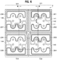
- FIG. 6 is a schematic plan view of the light emitting element according to the first embodiment showing a configuration of the electrodes.
- FIG. 7 is a schematic cross-sectional view of the light emitting element according to the first embodiment taken along a line VII-VII in FIG. 6 .
- FIG. 8A is a schematic plan view for explaining a layer structure of the light emitting element according to the first embodiment, in which arrangement regions of an n-side semiconductor layer and a p-side semiconductor layer are shown.
- FIG. 8B is a schematic plan view for explaining the layer structure of the light emitting element according to the first embodiment, in which arrangement regions of light-reflective electrodes are shown.
- FIG. 8C is a schematic plan view for explaining the layer structure of the light emitting element according to the first embodiment, in which an arrangement region of a first insulating layer is shown.
- FIG. 8D is a schematic plan view of a layer structure of the light emitting element according to the first embodiment, in which arrangement regions of wiring electrodes and the light-reflective metal layers are shown.
- FIG. 8E is a schematic plan view for explaining a layer structure of a light emitting element according to the first embodiment, in which an arrangement region of a second insulating layer is shown.
- FIG. 8F is a schematic plan view for explaining the layer structure of the light emitting element according to the first embodiment, in which arrangement regions of metal layers of bonding members are shown.
- FIG. 8G is a schematic plan view for explaining the layer structure of the light emitting element according to the first embodiment, in which arrangement regions of conductive members disposed on the metal layers in FIG. 8F are shown.
- FIG. 9A is a circuit diagram illustrating an equivalent circuit of a light emitting element according to a first variant example of the first embodiment.
- FIG. 9B is a circuit diagram illustrating an equivalent circuit of the light emitting element according to a second variant example of the first embodiment.
- FIG. 9C is a circuit diagram illustrating an equivalent circuit of the light emitting element according to the second variant example of the first embodiment, and is a simplified diagram of the circuit diagram in FIG. 9B .
- FIG. 10A is a circuit diagram illustrating an equivalent circuit of a light emitting element according to another variant example of the first embodiment.
- FIG. 10B is a circuit diagram illustrating an equivalent circuit of a light emitting element according to even another variant example of the first embodiment.
- FIG. 11A is a circuit diagram illustrating an equivalent circuit of a light emitting element according to a second embodiment.
- FIG. 11B is a circuit diagram illustrating an equivalent circuit of a light emitting element according to a variant example of the second embodiment.
- FIG. 12 is a schematic plan view of a light emitting device according to a third embodiment.
- FIG. 13 is a schematic plan view of a light emitting element according to the third embodiment showing a surface of the light emitting element at a substrate side.
- FIG. 14 is a circuit diagram illustrating an equivalent circuit of the light emitting element according to the third embodiment.
- FIG. 15A is a circuit diagram for illustrating a first measuring step in a method of inspecting a light emitting device according to the third embodiment.
- FIG. 15B is a circuit diagram for illustrating a second measuring step in the method of inspecting the light emitting device according to the third embodiment.
- FIG. 16A is a circuit diagram illustrating an equivalent circuit of the light emitting element according to a first variant example of the third embodiment.
- FIG. 16B is a circuit diagram illustrating an equivalent circuit of the light emitting element according to another variant example of the third embodiment.
- FIG. 16C is a circuit diagram illustrating an equivalent circuit of the light emitting element according to even another variant example of the third embodiment.
- a light emitting device will be described below.
- FIG. 4 The schematic cross-sectional view in FIG. 4 is taken along a IV-IV line, which is a polygonal line, in FIG. 3 .
- Distances and intervals in FIG. 4 are appropriately increased or reduced from distances and intervals (i.e., size of components) in FIG. 3 , and thus distances and intervals in FIG. 3 do not correspond to those in FIG. 4 .
- FIG. 6 is a plan view viewed from a reverse side of a plan view in FIG. 3 .
- the schematic cross-sectional view in FIG. 7 is taken along a VII-VII line, which is a polygonal line, in FIG. 6 .
- FIG. 7 is a schematic cross-sectional view taken in a state where the light emitting element in FIG. 4 is rotated by 180° showing a cross section similar to that in FIG. 4 .
- FIG. 8A to FIG. 8G components in the light emitting element that are sequentially layered from an upper surface side of a substrate 11 are shown in order to explain a layered structure of the light emitting element.
- a light emitting device 1 includes a light emitting element 2 , and a mounting substrate 3 .
- the mounting substrate 3 includes a plurality of wiring terminals 301 to 306 (first to sixth wiring terminals 301 to 306 ).
- the light emitting element 2 includes the substrate 11 , a plurality of light emitting cells 101 to 104 (first to fourth light emitting cells 101 to 104 ), a first insulating layer 16 , a plurality of wiring electrodes 141 to 145 (first to fifth wiring electrodes 141 to 145 ), and a second insulating layer 17 .
- FIG. 1 FIG.
- the light emitting element 2 further includes a plurality of bonding members 201 to 208 (first to eighth bonding members 201 to 208 ).
- Each of the bonding members 201 to 208 (first to eighth bonding members 201 to 208 ) is connected to a corresponding one of the wiring terminals 301 to 306 (first to sixth wiring terminals 301 to 306 ) of the mounting substrate 3 .
- a substrate 11 side of the light emitting element 2 may be referred to as a “lower side of the light emitting element 2 ”.
- the light emitting element 2 is mounted on the mounting substrate 3 such that the mounting substrate 3 faces an upper side of the light emitting element 2 .
- each of the light emitting cells 101 to 104 (first to fourth light emitting cells 101 to 104 ) is formed at an upper surface side of the substrate 11 , and includes a semiconductor layered body 12 including an n-side semiconductor layer 12 n and a p-side semiconductor layer 12 p in order from the upper surface side of the substrate 11 .
- the first insulating layer 16 covers an upper side of each of the light emitting cells 101 to 104 , and defines first n-side openings 16 n and first p-side openings 161 to 164 .
- Each of the first n-side openings 16 n and each of the first p-side openings 161 to 164 are defined at an upper side of a respective one of the light emitting cells 101 to 104 .
- the plurality of wiring electrodes 141 to 145 (first to fifth wiring electrodes 141 to 145 ) electrically connects the light emitting cells 101 to 104 on the substrate 11 in series.
- the second insulating layer 17 covers an upper side of each of the wiring electrodes 141 to 145 , and defines second n-side openings 172 , 174 , 176 , 178 and second p-side openings 171 , 173 , 175 , and 177 at an upper side of a respective one of the light emitting cells 101 to 104 .
- the light emitting cell 101 is referred to as a first light emitting cell
- the light emitting cell 102 is referred to as a second light emitting cell.
- three wiring electrodes 141 to 143 are connected to the first light emitting cell 101 and the second light emitting cell 102 .
- the first wiring electrode 141 is electrically connected to the p-side semiconductor layer 12 p of the first light emitting cell 101 via the first p-side opening 161 defined at an upper side of the first light emitting cell 101 .
- the second wiring electrode 142 is electrically connected to the n-side semiconductor layer 12 n of the first light emitting cell 101 via the first n-side openings 16 n defined at an upper side of the first light emitting cell 101 . Further, the wiring electrode 142 is electrically connected to the p-side semiconductor layer 12 p of the second light emitting cell 102 via the first p-side opening 162 defined at an upper side of the first light emitting cell 102 .
- the third wiring electrode 143 is electrically connected to the n-side semiconductor layer 12 n of the second light emitting cell 102 via the first n-side openings 16 n defined at an upper side of the first light emitting cell 102 .
- three wiring terminal 301 to 303 (first to third wiring terminals 301 to 303 ) are connected to the first light emitting cell 101 and the second light emitting cell 102 .
- the first wiring terminal 301 is electrically connected to the p-side semiconductor layer 12 p of the first light emitting cell 101 via the first bonding member 201 in the second p-side opening 171 that corresponds to the first light emitting cell 101 .
- the second wiring terminal 302 is electrically connected to the n-side semiconductor layer 12 n of the first light emitting cell 101 via the second bonding member 202 in the second n-side opening 172 that corresponds to the first light emitting cell 101 . Further, the second wiring terminal 302 is electrically connected to the p-side semiconductor layer 12 p of the second light emitting cell 102 via the third bonding member 203 in the second p-side opening 173 that corresponds to the second light emitting cell 102 .
- the third wiring terminal 303 is electrically connected to the n-side semiconductor layer 12 n of the second light emitting cell 102 via the fourth bonding member 204 in the second n-side opening 174 that corresponds to the second light emitting cell 102 .
- the second wiring electrode 142 is electrically connected to the n-side semiconductor layer 12 n of the first light emitting cell 101 and the p-side semiconductor layer 12 p of the second light emitting cell 102 . Further, the second bonding member 202 at an upper side of the first light emitting cell 101 and the third bonding member 203 at an upper side of the second light emitting cell 102 are electrically connected to the wiring electrode 142 , and are connected to the second wiring terminal 302 .
- first light emitting cell 101 and the second light emitting cell 102 are electrically connected to each other via a conduction path through the second wiring electrode 142 and a conduction path through the second wiring terminal 302 . Accordingly, if disconnection occurs in one of the two conduction paths, electrical conduction can be secured by the other of the two conduction paths. Thus, reliability of the light emitting device 1 according to the first embodiment can be increased.
- the mounting substrate 3 is a member for mounting the light emitting element 2 on an upper surface thereof. As shown in FIG. 2 , the mounting substrate 3 has a substantially rectangular shape in a plan view, and includes a base body 30 and a plurality of wiring terminals 301 to 306 (first to sixth wiring terminals 301 to 306 ) disposed on the base body 30 .
- the wiring terminals 301 to 306 are electrically insulated from each other, and as shown in FIG. 2 , are arranged in three rows and two columns at positions corresponding to positions where the bonding members 201 to 208 (first to eighth bonding members 201 to 208 ) of the light emitting element 2 are to be arranged.
- the first and sixth wiring terminals 301 and 306 can be used as a pair of wiring terminals for a power source, to each of which a respective one of wirings of an external power source such as an external driving circuit is to be connected.
- the first wiring terminal 301 is electrically connected to the first bonding member 201 that serves as a positive electrode of the light emitting element 2
- the sixth wiring terminal 306 is electrically connected to the eighth bonding member 208 that serves as a negative electrode of the light emitting element 2 .
- the external power source supplies electric power to the light emitting element 2 via the first and sixth wiring electrodes 301 and 306 and the first and eighth bonding members 201 and 208 . This allows the light emitting cells 101 to 104 (first to fourth light emitting cells 101 to 104 ) to emit light.
- the plurality of wiring terminals 301 to 306 also serves as reflective films for reflecting light emitted downward from the light emitting element 2 .
- a material having good electrical conductivity and a high reflectance with respect to a wavelength of light emitted from the light emitting element 2 is preferably used.
- a wiring pattern may be formed using, for example, Ti/Pt/Au.
- a single layer or a multi-layer that contains Ag, Al, Rh, etc. may be disposed on the surface of the wiring pattern.
- the base member 30 for example, ceramics such as aluminum nitride, metals, or resins may be used.
- the light emitting element 2 has a substantially square shape when viewed from above, and includes the substrate 11 , the semiconductor layered body 12 , light-reflective electrodes 13 , the first insulating layer 16 , and the wiring electrodes 141 to 145 (first to fifth wiring electrodes 141 to 145 ).
- the light emitting element 2 further includes a light-reflective metal layer 15 , which will be described below, the second insulating layer 17 , and the bonding members 201 to 208 (first to eighth bonding members 201 to 208 ).
- the substrate 11 serves to support the semiconductor layered body 12 . Further, the substrate 11 may be a growth substrate for epitaxially growing the semiconductor layered body 12 . In the case in which nitride semiconductors are used for the semiconductor layered body 12 , for example, a sapphire (Al 2 O 3 ) substrate can be used for the substrate 11 .
- the substrate 11 is disposed at a lower surface side of the light emitting element 2 .
- light is extracted mainly from a lower surface of the substrate 11 . That is, in the light emitting element 2 , a light extracting surface is a surface opposite to a surface at which the wiring electrodes 141 to 145 (first to fifth wiring electrodes 141 to 145 ), etc., are disposed, with respect to the semiconductor layered body 12 .
- the bonding members 201 to 208 are disposed at the upper surface side of the light emitting element 2 , and the light emitting element 2 has a structure suitable for a mounting in a face-down manner, which allows light to be extracted from the lower surface side of the substrate 11 .
- the semiconductor layered body 12 is disposed on the upper surface side of the substrate 11 .
- the n-side semiconductor layer 12 n and the p-side semiconductor layer 12 are layered in order from the side of the upper surface of the substrate 11 .
- the active layer 12 a is preferably disposed between the n-side semiconductor layer 12 n and the p-side semiconductor layer 12 p.
- the semiconductor layered body 12 is divided into four regions by a groove 12 d having a cross shape in which a longitudinal groove portion and a lateral groove portion, which extends in a lateral direction perpendicularly to the longitudinal groove portion, intersect.
- each of the four regions divided by the groove 12 d corresponds to a respective one of the light emitting cells 101 to 104 (first to fourth light emitting cells 101 to 104 ). That is, the light emitting cells 101 to 104 are electrically independent from one another except for being connected via the wiring electrodes 142 to 144 (second to fourth wiring electrodes 142 to 144 ), i.e., as the four regions of the semiconductor layered body 12 .
- Each of the light emitting cells 101 to 104 has a substantially square shape in the first embodiment, but may alternatively have another polygonal shape such as a rectangular shape or a hexagonal shape, a circular shape, an elliptical shape, or the like.
- the number of light emitting cells is not limited to four, and two or more light emitting cells are provided.
- electrical connections among the plurality of light emitting cells is not limited to that all of the electrical connections are series connection, but the electrical connections may include a parallel connection.
- the semiconductor layered body 12 includes a first exposed region 12 b , which is a region where the p-side semiconductor layer 12 p and the active layer 12 a are absent and a portion of the n-side semiconductor layer 12 n recessed from the p-side semiconductor layer 12 p is exposed from the p-side semiconductor layer 12 p .
- Each of the light emitting cells 101 to 104 includes six first exposed portions 12 b , each of which has a substantially circular shape when viewed from above.
- a second exposed region 12 c which is a region where the p-side semiconductor layer 12 p and the active layer 12 a are absent and a portion of the n-side semiconductor layer 12 n is exposed, is formed.
- n-side semiconductor layer 12 n the active layer 12 a , and the p-side semiconductor layer 12 p , for example, a nitride semiconductor such as In X Al Y Ga 1-X-Y N (0 ⁇ X, 0 ⁇ Y, X+Y ⁇ 1) can be used.
- a nitride semiconductor such as In X Al Y Ga 1-X-Y N (0 ⁇ X, 0 ⁇ Y, X+Y ⁇ 1) can be used.
- each of the light-reflective electrodes 13 is disposed at an upper surface side of the p-side semiconductor layer 12 p .
- Each of the light-reflective electrodes 13 serves as a current diffusion layer for diffusing current supplied from a respective one of the wiring electrodes 141 to 145 (first to fifth wiring electrodes 141 to 145 ) over a wide area in the p-side semiconductor layer 12 p , and as a light-reflective layer.
- Each of the light-reflective electrodes 13 is disposed on substantially an entirety of an upper surface of the p-side semiconductor layer 12 p of a respective one of the light emitting cells 101 to 104 (first to fourth light emitting cells 101 to 104 ).
- Each of the light reflective electrodes 13 preferably includes a metal layer made of a metal material that has good electrical conductivity and good reflectivity. Examples of such a metal material include Ag, Al and an alloy of these metals.
- the first insulating layer 16 is disposed on an upper surface side of the semiconductor layered body 12 and an upper surface side of the light-reflective electrodes 13 . As shown in FIG. 7 and FIG. 8C , the first insulating layer 16 continuously covers lateral surfaces of the semiconductor layered structure 12 of each of the light emitting cells 101 to 104 (first to fourth light emitting cells 101 to 104 ), regions between the lateral surfaces of the semiconductor layered structure 12 of the light emitting cells 101 to 104 , lateral surfaces 13 a and an upper surface of each of the light-reflective electrodes 13 , and the second exposed portions 12 c .
- the expression the “regions between the lateral surfaces of the semiconductor layered structure 12 ” refers to, more specifically, the first exposed portions 12 b and the groove 12 d of each of the light emitting cells 101 to 104 .
- the first insulating layer 16 defines a plurality of the first n-side openings 16 n in each of the light emitting cells 101 to 104 .
- Each of the first n-side openings 16 n has a circular shape and defined at a region where a respective one of the first exposed portions 12 b is provided.
- Each of the wiring electrodes 142 to 145 (second to fifth wiring electrodes 142 to 145 ) on the first insulating layer 16 is electrically connected to the n-side semiconductor layer 12 n in corresponding ones of the first n-side openings 16 n.
- the first insulating layer 16 defines the first p-side openings 161 to 164 , each of which has a comb-like shape, in regions where the light-reflective electrodes 13 are disposed.
- Each of the wiring electrodes 141 to 144 (first to fourth wiring electrodes 141 to 144 ) on the first insulating layer 16 is electrically connected to the p-side semiconductor layer 12 p via a respective one of the light-reflective electrodes 13 in a respective one of the first p-side openings 161 to 164 .
- the first insulating layer 16 protects the semiconductor layered structure 12 and the light-reflective electrodes 13 , and insulates between each of the wiring electrodes 141 to 145 (first to fifth wiring electrodes 141 to 145 ) and the semiconductor layered structure 12 and between the light-reflective metal layer 15 and the semiconductor layered structure 12 .
- oxide or nitride containing at least one selected from the group consisting of Si, Ti, Zr, Nb, Ta, Al, and Hf can be used.
- SiO 2 which has a high light-transmissivity with respect to visible light and a low refractive index, is preferably used.
- the wiring electrodes 141 to 145 are disposed at the upper surface side of the semiconductor layered structure 12 , the light-reflective electrodes 13 , and the first insulating layer 16 .
- a respective one of the wiring electrodes 142 to 145 (second to fifth wiring electrodes 142 to 145 ) is electrically connected to the n-side semiconductor layer 12 n in the first n-side openings 16 n of the first insulating layer 16 at the first exposed regions 12 b.
- Each of the wiring electrodes 141 to 144 (first to fourth wiring electrodes 141 to 144 ) is electrically connected to the p-side semiconductor layer 12 p via the light-reflective electrode 13 in a respective one of the first p-side openings 161 to 164 above a respective one of the light-reflective electrodes 13 via the respective one of the light-reflective electrodes 13 .
- each of the wiring electrodes 141 to 145 serves as both a pad electrode of a respective one of the light emitting cells 101 to 104 (first to fourth light emitting cells 101 to 104 ) and a wiring that connects corresponding ones of the light emitting cells 101 to 104 .
- pad electrodes may be disposed separately from the light emitting cells 101 to 104 , and each of the wiring electrodes 141 to 145 may be connected to a respective one of the pad electrodes.
- the wiring electrodes 141 to 145 cover the lateral surfaces of the light emitting cells 101 to 104 and regions therebetween via the first insulating layer 16 .
- the first wiring electrode 141 continuously covers an upper surface and lateral surfaces of the first light emitting cell 101 .
- the second wiring electrode 142 continuously covers an upper surface and lateral surfaces of each of the first light emitting cell 101 and the second light emitting cell 102 , and a region between the lateral surfaces of the first light emitting cell 101 and the second light emitting cell 102 .
- the third wiring electrode 143 electrically connects the n-side semiconductor layer 12 n of the second light emitting cell 102 and the p-side semiconductor layer 12 p of the third light emitting cell 103 .
- the third wiring electrode 143 continuously covers an upper surface and lateral surfaces of the second and third light emitting cells 102 and 103 and a region between the lateral surfaces of light emitting cells 102 and 103 .
- the fourth wiring electrode 144 electrically connects the n-side semiconductor layer 12 n of the third light emitting cell 103 and the p-side semiconductor layer 12 p of the fourth light emitting cell 104 .
- the fourth wiring electrode 144 continuously covers an upper surface and lateral surfaces of each of the third and fourth light emitting cells 103 and 104 , and a region between the lateral surfaces of the light emitting cells 103 and 104 .
- the fifth wiring electrode 145 electrically connects the n-side semiconductor layer 12 n of the fourth light emitting cell 104 and the eighth bonding member 208 .
- the fifth wiring electrode 145 continuously covers the upper surface and lateral surfaces of the emitting cell 104 .
- arranging the wiring electrodes 142 to 144 (second to fourth wiring electrodes 142 to 144 ) successively on the plurality of light emitting cells 101 to 104 (first to fourth light emitting cells 101 to 104 ) allows the wiring electrodes 142 to 144 to be disposed on the groove 12 d formed between adjacent ones of the light emitting cells 101 to 104 .
- the semiconductor layered structure 12 is removed at the groove 12 d , so that height difference is increased between the upper surface of each semiconductor layered structure 12 and a bottom surface of the groove 12 d .
- the wiring electrodes 142 to 144 (second to fourth wiring electrodes 142 to 144 ) are not easily disposed in the groove 12 d , and portions of the wiring electrodes 142 to 144 in the groove 12 d tends to have a lower quality.
- the first insulating layer 16 is not easily formed, which may have a bad effect on the wiring electrodes 142 to 144 on the first insulating layer 16 . Due to these factors, disconnection may occur in portions of the wiring electrodes 142 to 144 in the groove 12 d .
- two conductive paths that is, an electrical conduction path through the second wiring electrode 142 and an electrical conduction path through the second wiring terminal 302 . Accordingly, even if disconnection occurs in one of the conduction paths, electrical conduction between the first light emitting cell 101 and the second light emitting cell 102 can be secured. More specifically, even if disconnection occurs in the conduction path through the second wiring electrode 142 , which have a possibility of disconnection, electrical conduction can be secured by the conduction path through the second wiring terminal 302 . Accordingly, reliability of the light emitting device 1 can be improved.
- electrical resistance of the wiring electrodes 141 to 145 is lower than electrical resistance of the wiring terminals 301 to 306 (first to sixth wiring terminals 301 to 306 ) and the bonding members 201 to 208 (first to eighth bonding members 201 to 208 ), so that current flows mainly in the conduction path through the wiring electrodes 141 to 145 .
- Each of the wiring electrodes 141 to 145 (first to fifth wiring electrodes 141 to 145 ) preferably disposed to cover at least a portion of each of the lateral surfaces of corresponding one or more of the light emitting cells 101 to 104 (first to fourth light emitting cells 101 to 104 ), and is more preferably disposed to continuously cover lateral surfaces of the active layer 12 a of corresponding one or more of the light emitting cells 101 to 104 .
- each of the wiring electrodes 141 to 145 can reflect light emitted from the lateral surfaces of each of the light emitting cells 101 to 104 , and light leaked from the lateral surfaces of the light emitting cells 101 to 104 can be reduced, so that light extraction efficiency of the light emitting device 1 can be increased.
- Each of the wiring electrodes 141 to 145 (first to fifth wiring electrodes 141 to 145 ) preferably includes a metal layer made of a metal material having good conductivity and good reflectivity.
- a metal material include Ag, Al and an alloy of these metals.
- Al and Al alloy respectively have a high light reflectivity, and less easily migrates than Ag, and thus can be suitably used for the wiring electrodes 141 to 145 .
- the light-reflective metal layer 15 is disposed on the upper surface side of the first insulating layer 16 in a region where the wiring electrodes 141 to 145 (first to fifth wiring electrodes 141 to 145 ) are not disposed.
- the light-reflective metal layer 15 is a light-reflective metal layer continuously covering lateral surfaces of the light emitting cells 101 to 104 (first to fourth light emitting cells 101 to 104 ) and a region therebetween, i.e., the second exposed portions 12 c and the groove 12 d , via the first insulating layer 16 .
- the light-reflective metal layer a material similar to a material of the wiring electrodes 141 to 145 (first to fifth wiring electrodes 141 to 145 ) can be used.
- the light-reflective metal layer 15 is not electrically connected to any one of the wiring electrodes 141 to 145 .
- the second insulating layer 17 is disposed on the upper surface side of first insulating layer 16 , the upper surface side of the wiring electrodes 141 to 145 (first to fifth wiring electrodes 141 to 145 ), and the upper surface side of the light-reflective electrodes 15 .
- the second insulating layer 17 defines a second p-side opening 171 on a portion of an upper surface of the first wiring electrode 141 .
- the second insulating layer 17 defines a second n-side opening 172 and a second p-side opening 173 on portions of an upper surface of the second wiring electrode 142 .
- the second insulating layer 17 defines a second n-side opening 174 and a second p-side opening 175 on portions of an upper surface of the third wiring electrode 143 .
- the second insulating layer 17 defines a second n-side opening 176 and a second p-side opening 177 on portions of an upper surface of the fourth wiring electrode 144 .
- the second insulating layer 17 defines a second p-side opening 178 on a portion of an upper surface of the fifth wiring electrode 145 .
- the second p-side openings 171 , 173 , 175 , and 177 and the second n-side openings 172 , 174 , 176 , and 178 respectively have a comb-like shape in the first embodiment, but any appropriate number and shapes of the second p-side openings and the second n-side openings may be employed.
- Each of the second p-side openings 171 , 173 , 175 , and 177 of the second insulating layer 17 has an E-shape when viewed from above, which is substantially the same as the shape of each of the first p-side openings 161 , 162 , 163 , and 164 of the first insulating layer 16 when viewed from above. Further, each of the second p-side openings 171 , 173 , 175 , and 177 has an area smaller than an area of a respective one of the first p-side openings 161 , 162 , 163 , and 164 .
- the second insulating layer 17 is a protective film that protects the wiring electrodes 141 to 145 (first to fifth wiring electrodes 141 to 145 ) and the light-reflective metal layer 15 .
- a material similar to a material used for the first insulating layer 16 is preferably used. Meanwhile, different materials may be used for the first insulating layer 16 and the second insulating layer 17 .
- the bonding members 201 to 208 are disposed on the upper surface side of the wiring electrodes 141 to 145 (first to fifth wiring electrodes 141 to 145 ) and the upper surface side of second insulating layer 17 .
- Each of the bonding members 201 to 208 is a member for electrically connecting a corresponding one of the wiring electrodes 141 to 145 and a corresponding one of the wiring terminals 301 to 306 (first to fifth wiring terminals 301 to 306 ).
- the bonding members 201 to 208 include metal layers 181 to 188 , and conductive members 191 to 198 on the metal layers 181 to 188 , respectively.
- each of the metal layers 181 to 188 has an E-shape when viewed from above, which is substantially the same as the shape of each of the second p-side and n-side openings 171 to 178 of the second insulating layer 17 when viewed from above.
- Each of the metal layers 181 to 188 has an area larger than an area of a respective one of the second p-side and n-side openings 171 to 178 of the second insulating layer 17 .
- the first bonding member 201 is connected to the upper surface of the first wiring electrode 141 in the second p-side opening 171 of the second insulating layer 17 . Further, the first wiring electrode 141 is electrically connected to the p-side semiconductor layer 12 p of the first light emitting cell 101 in the first p-side opening 161 of the first insulating layer 16 via the light-reflective electrode 13 . Thus, the first bonding member 201 functions as a p-side electrode of the first light emitting cell 101 .
- the second bonding member 202 is connected to the upper surface of the second wiring electrode 142 in the second n-side opening 172 of the second insulating layer 17 . Further, the second wiring electrode 142 is electrically connected to the n-side semiconductor layer 12 n of the first light emitting cell 101 in the first n-side openings 16 n of the first insulating layer 16 . Thus, the second bonding member 202 functions as an n-side electrode of the first light emitting cell 101 .
- the third bonding member 203 is connected to the upper surface of the second wiring electrode 142 in the second p-side opening 173 of the second insulating layer 17 . Further, the second wiring electrode 142 is electrically connected to the p-side semiconductor layer 12 p of the first light emitting cell 102 in the first p-side opening 162 of the first insulating layer 16 via the light-reflective electrode 13 . Thus, the third bonding member 203 functions as a p-side electrode of the second light emitting cell 102 .
- the fourth bonding member 204 is connected to the upper surface of the third wiring electrode 143 in the second n-side opening 174 of the second insulating layer 17 . Further, the third wiring electrode 143 is electrically connected to the n-side semiconductor layer 12 n of the second light emitting cell 102 in the first n-side openings 16 n of the first insulating layer 16 . Thus, the fourth bonding member 204 functions as an n-side electrode of the second light emitting cell 102 .
- the fifth bonding member 205 is connected to the upper surface of the third wiring electrode 143 in the second p-side opening 175 of the second insulating layer 17 . Further, the third wiring electrode 143 is electrically connected to the p-side semiconductor layer 12 p of the third light emitting cell 103 in the first p-side opening 163 of the first insulating layer 16 via the light-reflective electrode 13 . Thus, the fifth bonding member 205 functions as a p-side electrode of the third light emitting cell 103 .
- the sixth bonding member 206 is connected to the upper surface of the fourth wiring electrode 144 in the second n-side opening 176 of the second insulating layer 17 . Further, the fourth wiring electrode 144 is electrically connected to the n-side semiconductor layer 12 n of the third light emitting cell 103 in the first n-side openings 16 n of the first insulating layer 16 . Thus, the sixth bonding member 206 functions as an n-side electrode of the third light emitting cell 103 .
- the seventh bonding member 207 is connected to the upper surface of the fourth wiring electrode 144 in the second p-side opening 177 of the second insulating layer 17 . Further, the fourth wiring electrode 144 is electrically connected to the p-side semiconductor layer 12 p of the first light emitting cell 104 in the first p-side opening 164 of the first insulating layer 16 via the light-reflective electrode 13 . Thus, the seventh bonding member 207 functions as a p-side electrode of the fourth light emitting cell 104 .
- the eighth bonding member 208 is connected to the upper surface of the fifth wiring electrode 145 in the second n-side opening 178 of the second insulating layer 17 . Further, the fifth wiring electrode 145 is electrically connected to the n-side semiconductor layer 12 n of the fourth light emitting cell 104 in the first n-side openings 16 n of the first insulating layer 16 . Thus, the eighth bonding member 208 functions as an n-side electrode of the fourth light emitting cell 104 .
- an entirety of each of the bonding member 201 to 208 is disposed at an inner side of a periphery of a corresponding one of the light emitting cells 101 to 104 (first to fourth light emitting cells 101 to 104 ).
- an entirety of the first bonding member 201 is disposed in a region where the first wiring electrode 141 is disposed in the first light emitting cell 101 .
- an entirety of the second bonding member 202 is disposed in a region where the second wiring electrode 142 is disposed in the first light emitting cell 101 .
- an entirety of the third bonding member 203 is disposed in a region where the second wiring electrode 142 is disposed in the second light emitting cell 102 . That is, the bonding members 201 to 208 (first to eighth bonding members 201 to 208 ) are disposed such that each of the bonding members 201 to 208 is not disposed over a plurality of wiring electrodes 141 to 145 (first to fifth wiring electrodes 141 to 145 ) with different electric potentials among the wiring electrodes 141 to 145 on the light emitting cells 101 to 104 (first to fourth light emitting cells 101 to 104 ).
- a potential difference between each of the bonding members 201 to 208 and a corresponding one of the wiring electrodes 141 to 145 can be reduced, compared with a configuration in which each of the bonding members 201 to 208 is disposed over, of the wiring electrodes 141 to 145 , wiring electrodes that have different electric potentials. Accordingly, for example, if the second insulating layer 17 has defects, migration of a metal material between the bonding members 201 to 208 and the wiring electrodes 141 to 145 can be reduced.
- the first and second bonding members 201 and 208 serve as electrodes to which the first and sixth wiring terminals 301 and 306 of the mounting substrate 3 are connected, respectively.
- the bonding members 202 to 207 (second to seventh bonding members 202 to 207 ) serve as electrodes to each of which a corresponding one of the wiring terminals 302 to 305 (second to fifth wiring terminals 302 to 305 ) of the mounting substrate 3 are connected.
- each of the bonding members 201 to 208 is connected to corresponding one of the wiring terminals 301 to 306 , allowing for determining a specific light emitting cell in which leakage occurs among the light emitting cells 101 to 104 (first to fourth light emitting cells 101 to 104 ) electrically connected to each other via the bonding members 201 to 208 .
- Occurrence of leakage current in a specific light emitting cell can be determined, for example, in the light emitting cell 101 connected to the first bonding member 201 and the second bonding member 202 , by applying voltage between the first wiring terminal 301 , which is electrically connected to the first bonding member 201 , and the second wiring terminal 302 , which is electrically connected to the second bonding member 202 , and measuring a current value.
- the metal layers 181 to 188 are seed layers for forming the conductive members 191 to 198 , respectively, by using a plating method.
- the seed layers are metal layers that serve as current paths at the time of forming the conductive members 191 to 198 , and can be formed by using a sputtering method, a vapor deposition, or the like.
- Each of the seed layers preferably includes a metal layer made of a metal material having good conductivity and good reflectivity. Examples of such a metal material include Al, Ag, Al alloy, and Ag alloy.
- the seed layers is preferably disposed such that the metal layer made of Al, Ag, Al alloy or Ag alloy is in contact with the second insulating layer 17 . With this arrangement, light emitted from the light emitting cells 101 to 104 (first to fourth light emitting cells 101 to 104 ) can be efficiently reflected toward a second insulating layer 17 side.
- Examples of a material of the conductive members 191 to 198 include metals such as Cu, Au, and Ni. Further, each of the conductive members 191 to 198 may have a layered structure in which a plurality of metals are used. In order to prevent corrosion and enhance bondability with the mounting substrate via an Au alloy-based bonding material such as Au—Sn eutectic solder, at least an uppermost layer of each of the conductive members 191 to 198 is preferably made of Au.
- the second wiring terminal 302 on the mounting substrate 3 is electrically connected to the n-side semiconductor layer 12 n of the first light emitting cell 101 via the second bonding member 202 , and is electrically connected to the p-side semiconductor layer 12 p of the second light emitting cell 102 via the third bonding member 203 .
- first light emitting cell 101 and the second light emitting cell 102 are electrically connected to each other via the second wiring electrode 142 . More specifically, the second wiring electrode 142 electrically connects the n-side semiconductor layer 12 n of the first light emitting cell 101 and the p-side semiconductor layer 12 p of the second light emitting cell 102 .
- the third wiring terminal 303 on the mounting substrate 3 is electrically connected to the n-side semiconductor layer 12 n of the second light emitting cell 102 via the fourth bonding member 204 . Further, the fourth wiring terminal 304 on the mounting substrate 3 is electrically connected to the p-side semiconductor layer 12 p of the third light emitting cell 103 via the fifth bonding member 205 .
- the second and third light emitting cells 102 and 103 are electrically connected to each other via the third wiring electrode 143 . More specifically, the third wiring electrode 143 electrically connects the n-side semiconductor layer 12 n of the second light emitting cell 102 and the p-side semiconductor layer 12 p of the third light emitting cell 103 .
- the fifth wiring terminal 305 on the mounting substrate 3 is electrically connected to the n-side semiconductor layer 12 n of the third light emitting cell 103 via the sixth bonding member 206 , and is electrically connected to the p-side semiconductor layer 12 p of the fourth light emitting cell 104 via the seventh bonding member 207 .
- the third and fourth light emitting cells 103 and 104 are electrically connected to each other via the fourth wiring electrode 144 . More specifically, the fourth wiring electrode 144 electrically connects the n-side semiconductor layer 12 n of the third light emitting cell 103 and the p-side semiconductor layer 12 p of the fourth light emitting cell 104 .
- the light emitting device 1 when the external power source is connected to the light emitting device 1 , difference between, for example, the electric potential of the wiring terminals other than the first and sixth wiring terminals 301 and 306 and the electric potential of their corresponding wiring electrodes can be reduced. For example, as shown in FIG.
- the first wiring terminal 301 exhibits an electric potential of approximately 12V
- the first bonding member 201 , the first wiring electrode 141 , and the p-side semiconductor layer 12 p of the first light emitting cell 101 which are electrically connected to the first wiring terminal 301 , exhibit electric potentials of approximately 12V.
- the electric potential of the second wiring electrode 142 electrically connected to the n-side semiconductor layer 12 n of the first light emitting cell 101 is approximately 9V
- the electric potential of each of the second and third bonding members 202 and 203 , the second wiring terminal 302 , and the p-side semiconductor layer 12 p of the second light emitting cell 102 , which are electrically connected to the second wiring electrode 142 is approximately 9V. That is, there is substantially no difference between the electric potential of the second wiring terminal 302 of the mounting substrate 3 and the electric potential of each of the second and third bonding members 202 and 203 and the second wiring electrode 142 , which are electrically connected to the second wiring terminal 302 .
- the wiring electrodes 141 to 145 (first to fifth wiring electrodes 141 to 145 ) and the light-reflective metal layer 15 , light leaked from the lateral surfaces of the light emitting cells 101 to 104 (first to fourth light emitting cells 101 to 104 ) can be reduced, so that light extraction efficiency can be increased.
- the light extraction efficiency can be improved while maintaining reliability.
- the area of each of the wiring terminals 301 to 306 (first to sixth wiring terminals 301 to 306 ) on the mounting substrate 3 can be relatively increased, so that mountability between the light emitting element 2 and the mounting substrate 3 and heat dissipation performance can be increased.
- FIG. 9A is a circuit diagram illustrating an equivalent circuit of the light emitting element 2 A according to a first variant example of the first embodiment.
- an entirety of at least one of the bonding members 201 to 208 is disposed over two adjacent light emitting cells.
- a bonding member 212 shown in FIG. 9A corresponds to an integral body of the bonding member 202 and the bonding member 203 in FIG. 5B .
- the bonding member 212 can be formed by, for example, integrally forming the metal layers 182 and 183 shown in FIG. 8F , and similarly, integrally forming the conductive member 192 and 193 to form a single bonding member.
- the light emitting device according to the first variant example has an effect similar to that in the first embodiment.
- the wiring terminals 303 and 304 in the first embodiment corresponds to a single wiring terminal 313 in the first variant example.
- a mounting substrate including five wiring terminals 301 , 302 , 313 , 305 , and 306 that correspond to the light emitting element 2 A is illustrated, and the wiring terminal 303 and 304 in FIG. 5B collectively corresponds to a single terminal such as a wiring terminal 313 .
- respective adjacent light emitting cells electrically connected by a corresponding one of the wiring electrodes 142 to 144 are also electrically connected by a corresponding one of the wiring terminals 302 , 313 , and 305 .
- two conductive paths i.e., a conductive path through a respective one of the wiring electrodes and a conductive path through a respective one of the wiring terminals, are provided each of between a first light emitting cell 101 and a second light emitting cell 102 , between the second light emitting cell 102 and the light emitting cell 103 , and between the light emitting cell 103 and the light emitting cell 104 .
- electrical conductive path between respective ones of light emitting cells can be secured even if disconnection occurs in a portion of its corresponding wiring electrode or wiring terminal, in particular, a portion of its corresponding wiring terminal.
- the light emitting device according to the first variant example has an effect of enhancing reliability.
- FIG. 1 In FIG.
- a single bonding member 214 which corresponds to an integral body of the bonding member 204 and 205 , is disposed with respect to the wiring electrode 313 , but individual bonding members 204 and 205 as shown in FIG. 5B may alternatively be disposed.
- FIG. 9A a combination of the bonding member 212 in the first variant example and the wiring terminal 313 is shown, but these may not be used in combination and may be individually used.
- the four light emitting cells 101 to 104 are arranged in two rows and two columns when viewed from above and connected by the wiring electrodes 141 to 145 and the wiring terminals 301 to 306 in a folding manner, but other appropriate arrangement and/or connection may be alternatively employed.
- the four light emitting cells 101 to 104 are linearly arranged, and are connected via the wiring electrodes 141 to 145 and the wiring terminals 301 , 302 , 313 , 305 , and 306 .
- the same reference numerals will be applied to the components that have the same or similar structure as those shown in FIG. 9A and FIG. 9B , and descriptions thereof will be appropriately omitted.
- a bonding member 216 shown in FIG. 9B corresponds to an integral body of the bonding member 206 and the bonding member 207 in FIG. 9A .
- the wiring terminals 301 , 302 , 313 , 305 , and 306 and the bonding members 201 , 212 , 214 , 216 , and 208 are provided with one to one relation. Accordingly, by omitting illustration of the wiring terminals, which are indicated by two-dot chain lines, in FIG. 9B , a simple circuit diagram of a light emitting element as shown in FIG. 9C can be obtained.
- the simple equivalent circuit diagram of the light emitting element 21 shown in FIG. 9C is substantially equivalent to the equivalent circuit diagram of the light emitting element 2 B in FIG. 9B , in which the reference numerals of constituting components is changed from those in the light emitting element 2 B as below.
- a numeral “A” corresponds to the bonding member 201 , which functions as a positive electrode of the light emitting element 2 B.
- a numeral “C” corresponds to the bonding member 208 , which functions as a negative electrode of the light emitting element 2 B.
- a numeral “M” corresponds to each of the bonding members that function as electrodes between the numeral “A” and the numeral “C”.
- Each of the bonding members indicated by the numerals A, C, and M may be referred to as an electrode in the description below.
- a numeral “L” indicates each of the light emitting cells, and a numeral “E” corresponds to each of the wiring electrodes.
- Each of the numerals A, C, M, L and E may be provided with an identification number as necessary.
- four light emitting cells are provided, but other appropriate number of the light emitting cells may be alternatively provided.
- two light emitting cells L may be disposed as in the light emitting element 22 shown in FIG. 10A , or five light emitting cells L may be disposed as in the light emitting element 23 shown in FIG. 10B .
- a plurality of the light emitting cells L is disposed.
- a light emitting cell L is disposed between the electrode A and the electrode M, another light emitting cell L is disposed between the electrode M and the electrode M, and even another light emitting cell L is disposed between the electrode M and the electrode C. Accordingly, in a inspecting step in which the plurality of light emitting cells are inspected, if leakage occurs in any of the light emitting cells, the light emitting cell in which leakage occurs can be detected by applying voltage between the electrodes as described above and measuring a current value.
- a plurality of light emitting cells is disposed between the electrode A and the electrode M, and another plurality of light emitting cells is disposed between the electrode M and the electrode C. That is, in the light emitting device according to the present embodiment, the number of wiring terminals with respect to the number of the light emitting cells is smaller than in the light emitting device according to the variant examples of the first embodiment, and a plurality of light emitting cells is connected between the wiring terminals. More specifically, in the light emitting element 31 , two light emitting cells are connected between the wiring terminals 301 and 313 , and other two light emitting cells are connected between the wiring terminals 313 and 306 .
- the light emitting element according to the second embodiment has a structure such that, for example, the wiring terminals 302 and 305 and the bonding member 212 and 216 , which are arranged at both sides of the wiring terminal 313 in FIG. 9B to be connected with the bonding member 214 , are omitted from the equivalent circuit shown in FIG. 9B .
- This structure is equivalent to an equivalent circuit having a structure such that two electrodes M at both sides of an electrode M at the center of the light emitting element 21 in the simplified equivalent circuit diagram shown in FIG. 9C are omitted from the equivalent circuit shown in FIG. 9C .
- the two light emitting cells L which are connected between the wiring terminals 301 and 313 , are connected via the wiring electrodes E, so that the openings 176 and 177 for conducting between the bonding members shown in FIG. 8F and the semiconductor layered structure 12 may not be defined in the second insulating layer 17 .
- two light emitting cells L are disposed between the electrode A and the electrode M, and other two light emitting cells L are disposed between the electrode M and the electrode C, but any appropriate number of the light emitting cells L may be disposed between the electrode A and the electrode M and between the electrode M and the electrode C.
- a light emitting element 32 shown in FIG. 11B three light emitting cells L are disposed between the electrode A and the electrode M, and other three light emitting cells L are disposed between the electrode M and the electrode C.
- the light emitting device has an effect similar to that in the first embodiment and an effect as described below.
- regions where the wiring terminals corresponding to a corresponding one of light emitting cells are to be disposed are not easily secured.
- reduction in size of each of the wiring terminals allows the wiring terminals to be disposed on the regions, but may lead to deterioration of mountability between the light emitting element and the mounting substrate and heat dissipation performance.
- the number of the wiring terminals can be reduced, and the area of each of the wiring terminals 301 to 306 on the mounting substrate 3 can be relatively increased, so that mountability between the light emitting element 2 and the mounting substrate 3 and heat dissipation performance can be improved.
- a light emitting device will be described with reference to FIG. 12 to FIG. 14 .
- the same reference numerals will be applied to the components which have the same or similar structure as those shown in the first and second embodiments, and descriptions thereof will be appropriately omitted.
- connections between respective components in a cross-sectional direction can be referred in the cross-sectional views in FIGS. 4 and 7 and a layered structure of the light emitting element shown in FIGS. 8A to 8G .
- positional relationships between respective components in a plan view will be described.
- the light emitting device 1 C includes a light emitting element 2 C, and a mounting substrate 3 C.
- the light emitting element 2 C includes a substrate 11 , semiconductor layered structure 12 , light-reflective electrodes 13 , a first insulating layer 16 , and a second insulating layer 17 .
- a substrate-side surface of the light emitting element 2 C is shown, and illustration of some components are omitted for ease of explanation.
- the light emitting element 2 C includes first to sixth light emitting cells 101 to 106 . As shown in FIG. 13 , the light emitting element 2 C includes a plurality of wiring electrodes 141 a , 141 b , 142 , 143 a , 143 b , 144 a , and 144 b (which, in the third embodiment, may respectively corresponding to a first to a seventh wiring electrodes).
- the first insulating layer 16 covers an upper side of each of the first to sixth light emitting cells 101 to 106 , and defines, at an upper side of each of the light emitting cells 101 to 106 , a plurality of first n-side openings 16 n and a respective one of first p-side openings 161 p , 162 p , 163 p , 164 p , 165 p , and 166 p.
- the first wiring electrode 141 a is electrically connected to a p-side semiconductor layer 12 p of the first light emitting cell 101 via the first p-side opening 161 defined above the first light emitting cell 101 .
- the second wiring electrode 141 b is electrically connected to the p-side semiconductor layer 12 p of the third light emitting cell 103 via the first p-side opening 163 p defined above the third light emitting cell 103 .
- the third wiring electrode 142 is electrically connected to an n-side semiconductor layer 12 n of the first light emitting cell 101 via the first n-side openings 16 n defined above the first light emitting cell 101 . Further, the third wiring electrode 142 is electrically connected to the p-side semiconductor layer 12 p of the second light emitting cell 102 via the first p-side opening 162 p defined above the second light emitting cell 102 . Even further, the third wiring electrode 142 is electrically connected to the n-side semiconductor layer 12 n of the third light emitting cell 103 via the first n-side openings 16 n defined above the third light emitting cell 103 .
- the third wiring electrode 142 is electrically connected to the p-side semiconductor layer 12 p of the fourth light emitting cell 104 via the first p-side opening 164 p defined above f the fourth light emitting cell 104 . That is, the third wiring electrode 142 is electrically connected to the light emitting cells 101 to 104 .
- the fourth wiring electrode 143 a is electrically connected to the n-side semiconductor layer 12 n of the second light emitting cell 102 via the first n-side openings 16 n defined above the second light emitting cell 102 . Further, the fourth wiring electrode 143 a is electrically connected to the p-side semiconductor layer 12 p of the fifth light emitting cell 105 via the first p-side opening 165 p defined above the second light emitting cell 105 .
- the fifth wiring electrode 143 b is electrically connected to the n-side semiconductor layer 12 n of the fourth light emitting cell 104 via the first n-side openings 16 n defined above the fourth light emitting cell 104 . Further, the fifth wiring electrode 143 b is electrically connected to the p-side semiconductor layer 12 p of the sixth light emitting cell 106 via the first p-side opening 166 p defined above the sixth light emitting cell 106 .
- the sixth wiring electrode 144 a is electrically connected to the n-side semiconductor layer 12 n of the fifth light emitting cell 105 via the first n-side openings 16 n defined above the fifth light emitting cell 105 .
- the seventh wiring electrode 144 b is electrically connected to the n-side semiconductor layer 12 n of the sixth light emitting cell 106 via the first n-side openings 16 n defined above the sixth light emitting cell 106 .
- the light-reflective metal layers 151 and 152 are disposed on at an upper surface side of the first insulating layer 16 in a region where the wiring electrodes (first electrode to seventh electrode) 141 a , 141 b , 142 , 143 a , 143 b , 144 a , and 44 b are not disposed.
- the second insulating layer 17 defines second p-side openings and second n-side openings. More specifically, the second insulating layer 17 defines a second p-side opening 171 p at the upper side of the first light emitting cell 101 , a second n-side opening 172 n at the upper side of the second light emitting cell 102 , a second p-side opening 173 p at the upper side of the third light emitting cell 103 , and a second n-side opening 174 n at the upper side of the fourth light emitting cell 104 .
- the second insulating layer 17 defines a second p-side opening 175 p and a second n-side opening 175 n at the upper side of the fifth light emitting cell 105 , and a second p-side opening 176 p and a second n-side opening 176 n at the upper side of the sixth light emitting cell 106 .
- the mounting substrate 3 C includes a base member 30 and a plurality of wiring terminals 321 to 326 , and the plurality of wiring terminals 321 to 326 are disposed at positions corresponding to positions on which the bonding members of the light emitting element 2 C, which is to be mounted, are to be arranged.
- the first wiring terminal 321 is electrically connected to the p-side semiconductor layer 12 p of the first light emitting cell 101 via the first bonding member 201 p in the second p-side opening 171 p that corresponds to the first light emitting cell 101 .
- the third wiring terminal 322 is electrically connected to the n-side semiconductor layer 12 n of the second light emitting cell 102 via the third bonding member 202 n in the second n-side opening 172 n that corresponds to the second light emitting cell 102 . Further, the third wiring terminal 322 is electrically connected to the p-side semiconductor layer 12 p of the fifth light emitting cell 105 via the fourth bonding member 205 p in the second p-side opening 175 p that corresponds to the fifth light emitting cell 105 .
- three wiring terminals 323 , 324 , 326 are connected to the third light emitting cell 103 , the fourth light emitting cell 104 , and the sixth light emitting cell 106 , respectively.
- the second wiring terminal 323 is electrically connected to the p-side semiconductor layer 12 p of the third light emitting cell 103 via the second bonding member 203 p in the second p-side opening 173 p that corresponds to the third light emitting cell 103 .
- the fourth wiring terminal 324 is electrically connected to the n-side semiconductor layer 12 n of the fourth light emitting cell 104 via the fourth bonding member 204 n in the second n-side opening 174 n that corresponds to the fourth light emitting cell 104 . Further, the fourth wiring terminal 324 is electrically connected to the p-side semiconductor layer 12 p of the second light emitting cell 106 via the sixth bonding member 206 p in the second p-side opening 176 p that corresponds to the sixth light emitting cell 106 .
- the sixth wiring terminal 326 is electrically connected to the eighth wiring electrode 144 b via the seventh bonding member 206 n .
- the seventh wiring electrode 144 b is electrically connected to the n-side semiconductor layer 12 n of the sixth light emitting cell 106 via the first n-side openings 16 n formed at an upper side of the sixth light emitting cell 106 .
- the first and second wiring terminals 321 and 323 are used for positive electrodes
- the fifth and sixth wiring terminals 325 and 326 are used for negative electrodes.
- the first wiring terminal 321 is electrically connected to the first bonding member 201 p that serves as a positive electrode of the light emitting element 2 C
- the fifth wiring terminal 325 is electrically connected to the fifth bonding member 205 n that serves as a negative electrode of the light emitting element 2 C.
- the second wiring terminal 323 is electrically connected to the second bonding member 203 p that serves as a positive electrode of the light emitting element 2 C
- the sixth wiring terminal 326 is electrically connected to the sixth bonding member 206 n that serves as a negative electrode of the light emitting element 2 C.
- the first, second, and fifth light emitting cells 101 , 102 , and 105 are configured to emit light when the external power source supplies electric power to the light emitting element 2 C via the first and fifth wiring electrodes 321 and 325 .
- the third, fourth, and sixth light emitting cells 103 , 104 , and 106 are configured to emit light when the external power source supplies electric power to the light emitting element 2 C via the second and sixth wiring electrodes 323 and 326 .
- Electric power may be supplied simultaneously to the first and fifth wiring electrodes 321 and 325 and the second and sixth wiring terminals 323 and 326 .
- the light emitting device has an effect similar to that in the first embodiment.
- leakage is failed to be detected unless leakage occurs in all of the light emitting cells connected between the wiring terminals.
- leakage that occurs in the other of the light emitting cells is failed to be detected.
- Occurrence of leakage in the light emitting cells of the light emitting device according to the third embodiment can be inspected by using a method as below.
- the method of inspecting the light emitting device includes a first measuring, a second measuring, and determining.
- first measuring voltage is applied between wiring terminals, and a current value through the plurality of light emitting cells connected between the wiring terminals is measured.
- second measuring voltage is applied between the wiring terminals that is the same as in the step of first measuring, and a current value through the plurality of light emitting cells connected between the wiring terminals is measured.
- the light emitting cell in which leakage is occurred is determined with reference to the current value measured in the step of first measuring and the step of second measuring.
- a method of inspecting the light emitting device according to the third embodiment will be more specifically described with reference to FIG. 15A and FIG. 15B .
- a power source and a current meter for applying voltage and measuring current, respectively, are connected between the wiring terminals 321 and 323 .
- a current value through the light emitting cells 101 and 103 which are connected between the wiring terminal 321 and the wiring terminal 323 , is measured. If a predetermined current value is measured, occurrence of leakage in any one of the light emitting cells 101 and 103 can be confirmed. If the predetermined current value is not measured, it is confirmed that a leak current does not flow, that is, leakage does not occur in the light emitting cell 103 .
- step of second measuring voltage is applied in a direction reverse to that in the first measuring, and a current value through the plurality of light emitting cells 101 and 103 , which are connected between the wiring terminals 321 and 323 , is measured. At this time, if a predetermined current value is measured, occurrence of leakage in any one of the light emitting cells 101 and 103 can be confirmed. If the predetermined current value is not measured, it is confirmed that a leak current does not flow, that is, leakage does not occur in the light emitting cell 103 .
- the light emitting cell in which leakage is occurred is determined with reference to the result of the first measuring and the result of the second measuring. For example, if a predetermined current value is measured in the step of first measuring and the predetermined current value is not measured in the step of second measuring, it is determined that leakage occurs in the light emitting cell 101 and does not occur in the light emitting cell 103 .
- the light emitting cell in which leakage occurs can be determined.
- a light emitting device in a light emitting device according to a variant example of the third embodiment, eight light emitting cells L 11 , L 12 , L 13 , L 14 , L 21 , L 22 , L 23 , and L 24 are connected to six wiring terminals 321 , 322 , 323 , 324 , 325 , and 326 and a plurality of wiring electrodes E 1 to E 8 .
- the variant example of the third embodiment is different from the third embodiment in that two wiring electrodes, each of which is as in the wiring electrode 142 in the third embodiment, that integrally connect four light emitting cells are disposed.
- a wiring electrode E 3 which is connected to four light emitting cells L 11 , L 12 , L 21 and L 22
- a wiring electrode E 6 which is electrically connected to four light emitting cells L 13 , L 14 , L 23 , and L 24 , are disposed.
- the inspection as described above is performed between respective wiring terminals, so that occurrence of leakage in the light emitting cells L 11 , L 14 , L 21 , and L 24 can be specified.
- the eight light emitting cells, the six bonding members A 1 , A 2 , C 1 , C 2 , M 11 , and M 21 , and the wiring terminal 321 to 326 are disposed, but any number of the light emitting cells, the bonding members, and the wiring terminals may be employed.
- two wiring electrodes E 2 and E 26 each of which connects its corresponding six light emitting cells arranged in three rows and two columns, and wiring terminals, each of which corresponds to a respective one of the bonding members A 1 to A 3 , C 1 to C 3 , M 11 , M 21 , and M 31 , may be disposed.
- two wiring electrodes E 33 and E 36 each of which connects its corresponding eight light emitting cells arranged in four rows and two columns, and wiring terminals, may be disposed, and some of the bonding members may be integrally formed.
- a single bonding member A 1 and a single wiring terminal 331 may be disposed with respect to a single light emitting cell L 11
- a single bonding member A 2 and a single wiring terminal 332 may be disposed with respect to three light emitting cells L 21 , L 31 , and L 41 .
- the light emitting device is applicable for various light sources such as a backlight light source of a liquid crystal display, various illumination devices, and a large-screen display.
Landscapes
- Engineering & Computer Science (AREA)
- Led Devices (AREA)
- Power Engineering (AREA)
- Microelectronics & Electronic Packaging (AREA)
- Led Device Packages (AREA)
- Physics & Mathematics (AREA)
- Condensed Matter Physics & Semiconductors (AREA)
- General Physics & Mathematics (AREA)
- Computer Hardware Design (AREA)
Abstract
Description
Claims (22)
Applications Claiming Priority (2)
| Application Number | Priority Date | Filing Date | Title |
|---|---|---|---|
| JP2017075482A JP6928233B2 (en) | 2017-04-05 | 2017-04-05 | Light emitting device |
| JP2017-075482 | 2017-04-05 |
Publications (2)
| Publication Number | Publication Date |
|---|---|
| US20180294391A1 US20180294391A1 (en) | 2018-10-11 |
| US10553770B2 true US10553770B2 (en) | 2020-02-04 |
Family
ID=63711281
Family Applications (1)
| Application Number | Title | Priority Date | Filing Date |
|---|---|---|---|
| US15/945,172 Active US10553770B2 (en) | 2017-04-05 | 2018-04-04 | Light emitting device including light emitting element with multiple light emitting cells |
Country Status (2)
| Country | Link |
|---|---|
| US (1) | US10553770B2 (en) |
| JP (1) | JP6928233B2 (en) |
Families Citing this family (7)
| Publication number | Priority date | Publication date | Assignee | Title |
|---|---|---|---|---|
| EP3528889A4 (en) * | 2016-10-21 | 2020-06-03 | Ohio State Innovation Foundation | Antimicrobial wound care dressing |
| JP6756346B2 (en) * | 2018-06-29 | 2020-09-16 | 日亜化学工業株式会社 | Manufacturing method of light emitting module |
| KR102619665B1 (en) * | 2018-06-29 | 2023-12-29 | 삼성전자주식회사 | Light emitting device |
| US11227985B2 (en) | 2019-03-28 | 2022-01-18 | Nichia Corporation | Light-emitting device |
| KR20200026776A (en) * | 2019-11-29 | 2020-03-11 | 엘지전자 주식회사 | Display device using semiconductor light emitting device and method for manufacturing the same |
| EP4040514B1 (en) | 2021-02-04 | 2025-05-21 | Nichia Corporation | Light emitting element and light emitting device |
| US12155011B2 (en) | 2021-02-08 | 2024-11-26 | Nichia Corporation | Light emitting element and light emitting device |
Citations (8)
| Publication number | Priority date | Publication date | Assignee | Title |
|---|---|---|---|---|
| US20080210954A1 (en) | 2005-08-08 | 2008-09-04 | Seoul Opto-Device Co., Ltd. | Alternating Current Light Emitting Device |
| US20080211416A1 (en) | 2007-01-22 | 2008-09-04 | Led Lighting Fixtures, Inc. | Illumination devices using externally interconnected arrays of light emitting devices, and methods of fabricating same |
| US20090267085A1 (en) | 2005-03-11 | 2009-10-29 | Seoul Semiconductor Co., Ltd. | Led package having an array of light emitting cells coupled in series |
| US20100019253A1 (en) | 2007-03-13 | 2010-01-28 | Dae Won Kim | Ac light emitting diode |
| US20120074441A1 (en) * | 2010-09-24 | 2012-03-29 | Seoul Semiconductor Co., Ltd. | Wafer-level light emitting diode package and method of fabricating the same |
| US20130264592A1 (en) * | 2012-04-09 | 2013-10-10 | Cree, Inc. | Wafer level packaging of multiple light emitting diodes (leds) on a single carrier die |
| JP2016012707A (en) | 2014-06-30 | 2016-01-21 | 晶元光電股▲ふん▼有限公司 | Photoelectric component and manufacturing method of the same |
| US20160064611A1 (en) * | 2014-09-02 | 2016-03-03 | Pun Jae Choi | Semiconductor light-emitting device |
Family Cites Families (8)
| Publication number | Priority date | Publication date | Assignee | Title |
|---|---|---|---|---|
| JP4045767B2 (en) * | 2001-09-28 | 2008-02-13 | 日亜化学工業株式会社 | Semiconductor light emitting device |
| EP2475006B1 (en) * | 2003-07-16 | 2015-09-30 | Panasonic Intellectual Property Management Co., Ltd. | Semiconductor light emitting device, method of manufacturing the same, and lighting apparatus and display apparatus using the same |
| US7221044B2 (en) * | 2005-01-21 | 2007-05-22 | Ac Led Lighting, L.L.C. | Heterogeneous integrated high voltage DC/AC light emitter |
| US8034860B2 (en) * | 2006-07-21 | 2011-10-11 | Eastman Specialties Holdings Corporation | Organosol plastisol compositions |
| JP2008192797A (en) * | 2007-02-05 | 2008-08-21 | Sony Corp | LIGHT SOURCE MODULE AND ITS MANUFACTURING METHOD, LIGHT SOURCE DEVICE, AND LIQUID CRYSTAL DISPLAY DEVICE |
| TW201322437A (en) * | 2011-11-17 | 2013-06-01 | 海立爾股份有限公司 | High voltage AC light emitting diode structure |
| KR101186684B1 (en) * | 2012-03-29 | 2012-09-28 | 서울옵토디바이스주식회사 | Light emitting diode and method of fabricating the same |
| JP6176032B2 (en) * | 2013-01-30 | 2017-08-09 | 日亜化学工業株式会社 | Semiconductor light emitting device |
-
2017
- 2017-04-05 JP JP2017075482A patent/JP6928233B2/en active Active
-
2018
- 2018-04-04 US US15/945,172 patent/US10553770B2/en active Active
Patent Citations (12)
| Publication number | Priority date | Publication date | Assignee | Title |
|---|---|---|---|---|
| US20090267085A1 (en) | 2005-03-11 | 2009-10-29 | Seoul Semiconductor Co., Ltd. | Led package having an array of light emitting cells coupled in series |
| JP2011066463A (en) | 2005-03-11 | 2011-03-31 | Seoul Semiconductor Co Ltd | Light-emitting element having plurality of light-emitting cells |
| US20080210954A1 (en) | 2005-08-08 | 2008-09-04 | Seoul Opto-Device Co., Ltd. | Alternating Current Light Emitting Device |
| JP2009505393A (en) | 2005-08-08 | 2009-02-05 | ソウル オプト デバイス カンパニー リミテッド | AC light emitting device |
| US20080211416A1 (en) | 2007-01-22 | 2008-09-04 | Led Lighting Fixtures, Inc. | Illumination devices using externally interconnected arrays of light emitting devices, and methods of fabricating same |
| JP2010517274A (en) | 2007-01-22 | 2010-05-20 | クリー レッド ライティング ソリューションズ、インコーポレイテッド | Illumination device using array of light-emitting elements interconnected externally and method of manufacturing the same |
| US20100019253A1 (en) | 2007-03-13 | 2010-01-28 | Dae Won Kim | Ac light emitting diode |
| JP2010521807A (en) | 2007-03-13 | 2010-06-24 | ソウル オプト デバイス カンパニー リミテッド | AC drive type light emitting diode |
| US20120074441A1 (en) * | 2010-09-24 | 2012-03-29 | Seoul Semiconductor Co., Ltd. | Wafer-level light emitting diode package and method of fabricating the same |
| US20130264592A1 (en) * | 2012-04-09 | 2013-10-10 | Cree, Inc. | Wafer level packaging of multiple light emitting diodes (leds) on a single carrier die |
| JP2016012707A (en) | 2014-06-30 | 2016-01-21 | 晶元光電股▲ふん▼有限公司 | Photoelectric component and manufacturing method of the same |
| US20160064611A1 (en) * | 2014-09-02 | 2016-03-03 | Pun Jae Choi | Semiconductor light-emitting device |
Also Published As
| Publication number | Publication date |
|---|---|
| JP6928233B2 (en) | 2021-09-01 |
| JP2018181942A (en) | 2018-11-15 |
| US20180294391A1 (en) | 2018-10-11 |
Similar Documents
| Publication | Publication Date | Title |
|---|---|---|
| US10553770B2 (en) | Light emitting device including light emitting element with multiple light emitting cells | |
| US10910536B2 (en) | Light emitting element | |
| US9293674B2 (en) | Light emitting device including light emitting element, outer connection electrodes and resin layer | |
| JP5754173B2 (en) | Light emitting unit and display device | |
| US11158767B2 (en) | Light-emitting element, light-emitting unit, light-emitting panel device, and method for driving light-emitting panel device | |
| US8188489B2 (en) | Light emitting diode for AC operation | |
| JP6176032B2 (en) | Semiconductor light emitting device | |
| US9366393B2 (en) | Light emitting device | |
| US20150076532A1 (en) | Light emitting diode | |
| US10937929B2 (en) | Semiconductor unit, semiconductor device, light-emitting apparatus, display apparatus, and method of manufacturing semiconductor device | |
| US10164153B2 (en) | Light-emitting element | |
| CN113257958A (en) | Light emitting diode test circuit, light emitting diode test method and manufacturing method | |
| US9929316B2 (en) | Light emitting element | |
| CN112840468A (en) | a light-emitting device | |
| US9368707B2 (en) | Mounting substrate and light-emitting device using the same | |
| US20180166498A1 (en) | Light-emitting devices | |
| US8957431B2 (en) | Semiconductor light emitting device having multi-cell array | |
| CN107026185B (en) | Light emitting element | |
| US20230335699A1 (en) | Light-emitting element, method for manufacturing light-emitting element, and light-emitting device | |
| JP7319551B2 (en) | light emitting device | |
| US20160260880A1 (en) | Light-emitting device using mounting substrate |
Legal Events
| Date | Code | Title | Description |
|---|---|---|---|
| AS | Assignment |
Owner name: NICHIA CORPORATION, JAPAN Free format text: ASSIGNMENT OF ASSIGNORS INTEREST;ASSIGNOR:EMURA, KEIJI;REEL/FRAME:045435/0330 Effective date: 20180330 |
|
| FEPP | Fee payment procedure |
Free format text: ENTITY STATUS SET TO UNDISCOUNTED (ORIGINAL EVENT CODE: BIG.); ENTITY STATUS OF PATENT OWNER: LARGE ENTITY |
|
| STPP | Information on status: patent application and granting procedure in general |
Free format text: RESPONSE TO NON-FINAL OFFICE ACTION ENTERED AND FORWARDED TO EXAMINER |
|
| STPP | Information on status: patent application and granting procedure in general |
Free format text: FINAL REJECTION MAILED |
|
| STPP | Information on status: patent application and granting procedure in general |
Free format text: ADVISORY ACTION MAILED |
|
| STPP | Information on status: patent application and granting procedure in general |
Free format text: DOCKETED NEW CASE - READY FOR EXAMINATION |
|
| STPP | Information on status: patent application and granting procedure in general |
Free format text: NOTICE OF ALLOWANCE MAILED -- APPLICATION RECEIVED IN OFFICE OF PUBLICATIONS |
|
| STPP | Information on status: patent application and granting procedure in general |
Free format text: PUBLICATIONS -- ISSUE FEE PAYMENT VERIFIED |
|
| STCF | Information on status: patent grant |
Free format text: PATENTED CASE |
|
| MAFP | Maintenance fee payment |
Free format text: PAYMENT OF MAINTENANCE FEE, 4TH YEAR, LARGE ENTITY (ORIGINAL EVENT CODE: M1551); ENTITY STATUS OF PATENT OWNER: LARGE ENTITY Year of fee payment: 4 |