US10545592B2 - Touch display module, method for driving the same, touch display panel and touch display device - Google Patents
Touch display module, method for driving the same, touch display panel and touch display device Download PDFInfo
- Publication number
- US10545592B2 US10545592B2 US15/554,173 US201715554173A US10545592B2 US 10545592 B2 US10545592 B2 US 10545592B2 US 201715554173 A US201715554173 A US 201715554173A US 10545592 B2 US10545592 B2 US 10545592B2
- Authority
- US
- United States
- Prior art keywords
- line
- touch
- driving transistor
- electrode
- pixel
- Prior art date
- Legal status (The legal status is an assumption and is not a legal conclusion. Google has not performed a legal analysis and makes no representation as to the accuracy of the status listed.)
- Active
Links
Images


Classifications
-
- G—PHYSICS
- G09—EDUCATION; CRYPTOGRAPHY; DISPLAY; ADVERTISING; SEALS
- G09G—ARRANGEMENTS OR CIRCUITS FOR CONTROL OF INDICATING DEVICES USING STATIC MEANS TO PRESENT VARIABLE INFORMATION
- G09G3/00—Control arrangements or circuits, of interest only in connection with visual indicators other than cathode-ray tubes
- G09G3/20—Control arrangements or circuits, of interest only in connection with visual indicators other than cathode-ray tubes for presentation of an assembly of a number of characters, e.g. a page, by composing the assembly by combination of individual elements arranged in a matrix no fixed position being assigned to or needed to be assigned to the individual characters or partial characters
- G09G3/22—Control arrangements or circuits, of interest only in connection with visual indicators other than cathode-ray tubes for presentation of an assembly of a number of characters, e.g. a page, by composing the assembly by combination of individual elements arranged in a matrix no fixed position being assigned to or needed to be assigned to the individual characters or partial characters using controlled light sources
- G09G3/30—Control arrangements or circuits, of interest only in connection with visual indicators other than cathode-ray tubes for presentation of an assembly of a number of characters, e.g. a page, by composing the assembly by combination of individual elements arranged in a matrix no fixed position being assigned to or needed to be assigned to the individual characters or partial characters using controlled light sources using electroluminescent panels
- G09G3/32—Control arrangements or circuits, of interest only in connection with visual indicators other than cathode-ray tubes for presentation of an assembly of a number of characters, e.g. a page, by composing the assembly by combination of individual elements arranged in a matrix no fixed position being assigned to or needed to be assigned to the individual characters or partial characters using controlled light sources using electroluminescent panels semiconductive, e.g. using light-emitting diodes [LED]
- G09G3/3208—Control arrangements or circuits, of interest only in connection with visual indicators other than cathode-ray tubes for presentation of an assembly of a number of characters, e.g. a page, by composing the assembly by combination of individual elements arranged in a matrix no fixed position being assigned to or needed to be assigned to the individual characters or partial characters using controlled light sources using electroluminescent panels semiconductive, e.g. using light-emitting diodes [LED] organic, e.g. using organic light-emitting diodes [OLED]
- G09G3/3225—Control arrangements or circuits, of interest only in connection with visual indicators other than cathode-ray tubes for presentation of an assembly of a number of characters, e.g. a page, by composing the assembly by combination of individual elements arranged in a matrix no fixed position being assigned to or needed to be assigned to the individual characters or partial characters using controlled light sources using electroluminescent panels semiconductive, e.g. using light-emitting diodes [LED] organic, e.g. using organic light-emitting diodes [OLED] using an active matrix
- G09G3/3258—Control arrangements or circuits, of interest only in connection with visual indicators other than cathode-ray tubes for presentation of an assembly of a number of characters, e.g. a page, by composing the assembly by combination of individual elements arranged in a matrix no fixed position being assigned to or needed to be assigned to the individual characters or partial characters using controlled light sources using electroluminescent panels semiconductive, e.g. using light-emitting diodes [LED] organic, e.g. using organic light-emitting diodes [OLED] using an active matrix with pixel circuitry controlling the voltage across the light-emitting element
-
- G—PHYSICS
- G06—COMPUTING OR CALCULATING; COUNTING
- G06F—ELECTRIC DIGITAL DATA PROCESSING
- G06F3/00—Input arrangements for transferring data to be processed into a form capable of being handled by the computer; Output arrangements for transferring data from processing unit to output unit, e.g. interface arrangements
- G06F3/01—Input arrangements or combined input and output arrangements for interaction between user and computer
- G06F3/03—Arrangements for converting the position or the displacement of a member into a coded form
- G06F3/041—Digitisers, e.g. for touch screens or touch pads, characterised by the transducing means
- G06F3/0412—Digitisers structurally integrated in a display
-
- G—PHYSICS
- G06—COMPUTING OR CALCULATING; COUNTING
- G06F—ELECTRIC DIGITAL DATA PROCESSING
- G06F3/00—Input arrangements for transferring data to be processed into a form capable of being handled by the computer; Output arrangements for transferring data from processing unit to output unit, e.g. interface arrangements
- G06F3/01—Input arrangements or combined input and output arrangements for interaction between user and computer
- G06F3/03—Arrangements for converting the position or the displacement of a member into a coded form
- G06F3/041—Digitisers, e.g. for touch screens or touch pads, characterised by the transducing means
- G06F3/0416—Control or interface arrangements specially adapted for digitisers
- G06F3/0418—Control or interface arrangements specially adapted for digitisers for error correction or compensation, e.g. based on parallax, calibration or alignment
- G06F3/04184—Synchronisation with the driving of the display or the backlighting unit to avoid interferences generated internally
-
- G—PHYSICS
- G06—COMPUTING OR CALCULATING; COUNTING
- G06F—ELECTRIC DIGITAL DATA PROCESSING
- G06F3/00—Input arrangements for transferring data to be processed into a form capable of being handled by the computer; Output arrangements for transferring data from processing unit to output unit, e.g. interface arrangements
- G06F3/01—Input arrangements or combined input and output arrangements for interaction between user and computer
- G06F3/03—Arrangements for converting the position or the displacement of a member into a coded form
- G06F3/041—Digitisers, e.g. for touch screens or touch pads, characterised by the transducing means
- G06F3/0416—Control or interface arrangements specially adapted for digitisers
- G06F3/0418—Control or interface arrangements specially adapted for digitisers for error correction or compensation, e.g. based on parallax, calibration or alignment
-
- G—PHYSICS
- G06—COMPUTING OR CALCULATING; COUNTING
- G06F—ELECTRIC DIGITAL DATA PROCESSING
- G06F3/00—Input arrangements for transferring data to be processed into a form capable of being handled by the computer; Output arrangements for transferring data from processing unit to output unit, e.g. interface arrangements
- G06F3/01—Input arrangements or combined input and output arrangements for interaction between user and computer
- G06F3/03—Arrangements for converting the position or the displacement of a member into a coded form
- G06F3/041—Digitisers, e.g. for touch screens or touch pads, characterised by the transducing means
- G06F3/044—Digitisers, e.g. for touch screens or touch pads, characterised by the transducing means by capacitive means
-
- G—PHYSICS
- G09—EDUCATION; CRYPTOGRAPHY; DISPLAY; ADVERTISING; SEALS
- G09G—ARRANGEMENTS OR CIRCUITS FOR CONTROL OF INDICATING DEVICES USING STATIC MEANS TO PRESENT VARIABLE INFORMATION
- G09G3/00—Control arrangements or circuits, of interest only in connection with visual indicators other than cathode-ray tubes
- G09G3/20—Control arrangements or circuits, of interest only in connection with visual indicators other than cathode-ray tubes for presentation of an assembly of a number of characters, e.g. a page, by composing the assembly by combination of individual elements arranged in a matrix no fixed position being assigned to or needed to be assigned to the individual characters or partial characters
- G09G3/22—Control arrangements or circuits, of interest only in connection with visual indicators other than cathode-ray tubes for presentation of an assembly of a number of characters, e.g. a page, by composing the assembly by combination of individual elements arranged in a matrix no fixed position being assigned to or needed to be assigned to the individual characters or partial characters using controlled light sources
- G09G3/30—Control arrangements or circuits, of interest only in connection with visual indicators other than cathode-ray tubes for presentation of an assembly of a number of characters, e.g. a page, by composing the assembly by combination of individual elements arranged in a matrix no fixed position being assigned to or needed to be assigned to the individual characters or partial characters using controlled light sources using electroluminescent panels
- G09G3/32—Control arrangements or circuits, of interest only in connection with visual indicators other than cathode-ray tubes for presentation of an assembly of a number of characters, e.g. a page, by composing the assembly by combination of individual elements arranged in a matrix no fixed position being assigned to or needed to be assigned to the individual characters or partial characters using controlled light sources using electroluminescent panels semiconductive, e.g. using light-emitting diodes [LED]
- G09G3/3208—Control arrangements or circuits, of interest only in connection with visual indicators other than cathode-ray tubes for presentation of an assembly of a number of characters, e.g. a page, by composing the assembly by combination of individual elements arranged in a matrix no fixed position being assigned to or needed to be assigned to the individual characters or partial characters using controlled light sources using electroluminescent panels semiconductive, e.g. using light-emitting diodes [LED] organic, e.g. using organic light-emitting diodes [OLED]
- G09G3/3225—Control arrangements or circuits, of interest only in connection with visual indicators other than cathode-ray tubes for presentation of an assembly of a number of characters, e.g. a page, by composing the assembly by combination of individual elements arranged in a matrix no fixed position being assigned to or needed to be assigned to the individual characters or partial characters using controlled light sources using electroluminescent panels semiconductive, e.g. using light-emitting diodes [LED] organic, e.g. using organic light-emitting diodes [OLED] using an active matrix
- G09G3/3233—Control arrangements or circuits, of interest only in connection with visual indicators other than cathode-ray tubes for presentation of an assembly of a number of characters, e.g. a page, by composing the assembly by combination of individual elements arranged in a matrix no fixed position being assigned to or needed to be assigned to the individual characters or partial characters using controlled light sources using electroluminescent panels semiconductive, e.g. using light-emitting diodes [LED] organic, e.g. using organic light-emitting diodes [OLED] using an active matrix with pixel circuitry controlling the current through the light-emitting element
-
- G—PHYSICS
- G09—EDUCATION; CRYPTOGRAPHY; DISPLAY; ADVERTISING; SEALS
- G09G—ARRANGEMENTS OR CIRCUITS FOR CONTROL OF INDICATING DEVICES USING STATIC MEANS TO PRESENT VARIABLE INFORMATION
- G09G3/00—Control arrangements or circuits, of interest only in connection with visual indicators other than cathode-ray tubes
- G09G3/20—Control arrangements or circuits, of interest only in connection with visual indicators other than cathode-ray tubes for presentation of an assembly of a number of characters, e.g. a page, by composing the assembly by combination of individual elements arranged in a matrix no fixed position being assigned to or needed to be assigned to the individual characters or partial characters
- G09G3/22—Control arrangements or circuits, of interest only in connection with visual indicators other than cathode-ray tubes for presentation of an assembly of a number of characters, e.g. a page, by composing the assembly by combination of individual elements arranged in a matrix no fixed position being assigned to or needed to be assigned to the individual characters or partial characters using controlled light sources
- G09G3/30—Control arrangements or circuits, of interest only in connection with visual indicators other than cathode-ray tubes for presentation of an assembly of a number of characters, e.g. a page, by composing the assembly by combination of individual elements arranged in a matrix no fixed position being assigned to or needed to be assigned to the individual characters or partial characters using controlled light sources using electroluminescent panels
- G09G3/32—Control arrangements or circuits, of interest only in connection with visual indicators other than cathode-ray tubes for presentation of an assembly of a number of characters, e.g. a page, by composing the assembly by combination of individual elements arranged in a matrix no fixed position being assigned to or needed to be assigned to the individual characters or partial characters using controlled light sources using electroluminescent panels semiconductive, e.g. using light-emitting diodes [LED]
- G09G3/3208—Control arrangements or circuits, of interest only in connection with visual indicators other than cathode-ray tubes for presentation of an assembly of a number of characters, e.g. a page, by composing the assembly by combination of individual elements arranged in a matrix no fixed position being assigned to or needed to be assigned to the individual characters or partial characters using controlled light sources using electroluminescent panels semiconductive, e.g. using light-emitting diodes [LED] organic, e.g. using organic light-emitting diodes [OLED]
- G09G3/3266—Details of drivers for scan electrodes
-
- G—PHYSICS
- G09—EDUCATION; CRYPTOGRAPHY; DISPLAY; ADVERTISING; SEALS
- G09G—ARRANGEMENTS OR CIRCUITS FOR CONTROL OF INDICATING DEVICES USING STATIC MEANS TO PRESENT VARIABLE INFORMATION
- G09G3/00—Control arrangements or circuits, of interest only in connection with visual indicators other than cathode-ray tubes
- G09G3/20—Control arrangements or circuits, of interest only in connection with visual indicators other than cathode-ray tubes for presentation of an assembly of a number of characters, e.g. a page, by composing the assembly by combination of individual elements arranged in a matrix no fixed position being assigned to or needed to be assigned to the individual characters or partial characters
- G09G3/22—Control arrangements or circuits, of interest only in connection with visual indicators other than cathode-ray tubes for presentation of an assembly of a number of characters, e.g. a page, by composing the assembly by combination of individual elements arranged in a matrix no fixed position being assigned to or needed to be assigned to the individual characters or partial characters using controlled light sources
- G09G3/30—Control arrangements or circuits, of interest only in connection with visual indicators other than cathode-ray tubes for presentation of an assembly of a number of characters, e.g. a page, by composing the assembly by combination of individual elements arranged in a matrix no fixed position being assigned to or needed to be assigned to the individual characters or partial characters using controlled light sources using electroluminescent panels
- G09G3/32—Control arrangements or circuits, of interest only in connection with visual indicators other than cathode-ray tubes for presentation of an assembly of a number of characters, e.g. a page, by composing the assembly by combination of individual elements arranged in a matrix no fixed position being assigned to or needed to be assigned to the individual characters or partial characters using controlled light sources using electroluminescent panels semiconductive, e.g. using light-emitting diodes [LED]
- G09G3/3208—Control arrangements or circuits, of interest only in connection with visual indicators other than cathode-ray tubes for presentation of an assembly of a number of characters, e.g. a page, by composing the assembly by combination of individual elements arranged in a matrix no fixed position being assigned to or needed to be assigned to the individual characters or partial characters using controlled light sources using electroluminescent panels semiconductive, e.g. using light-emitting diodes [LED] organic, e.g. using organic light-emitting diodes [OLED]
- G09G3/3275—Details of drivers for data electrodes
- G09G3/3291—Details of drivers for data electrodes in which the data driver supplies a variable data voltage for setting the current through, or the voltage across, the light-emitting elements
-
- H01L27/323—
-
- H—ELECTRICITY
- H10—SEMICONDUCTOR DEVICES; ELECTRIC SOLID-STATE DEVICES NOT OTHERWISE PROVIDED FOR
- H10K—ORGANIC ELECTRIC SOLID-STATE DEVICES
- H10K59/00—Integrated devices, or assemblies of multiple devices, comprising at least one organic light-emitting element covered by group H10K50/00
- H10K59/40—OLEDs integrated with touch screens
-
- G—PHYSICS
- G09—EDUCATION; CRYPTOGRAPHY; DISPLAY; ADVERTISING; SEALS
- G09G—ARRANGEMENTS OR CIRCUITS FOR CONTROL OF INDICATING DEVICES USING STATIC MEANS TO PRESENT VARIABLE INFORMATION
- G09G2300/00—Aspects of the constitution of display devices
- G09G2300/04—Structural and physical details of display devices
- G09G2300/0421—Structural details of the set of electrodes
- G09G2300/0426—Layout of electrodes and connections
-
- G—PHYSICS
- G09—EDUCATION; CRYPTOGRAPHY; DISPLAY; ADVERTISING; SEALS
- G09G—ARRANGEMENTS OR CIRCUITS FOR CONTROL OF INDICATING DEVICES USING STATIC MEANS TO PRESENT VARIABLE INFORMATION
- G09G2300/00—Aspects of the constitution of display devices
- G09G2300/04—Structural and physical details of display devices
- G09G2300/0421—Structural details of the set of electrodes
- G09G2300/043—Compensation electrodes or other additional electrodes in matrix displays related to distortions or compensation signals, e.g. for modifying TFT threshold voltage in column driver
-
- G—PHYSICS
- G09—EDUCATION; CRYPTOGRAPHY; DISPLAY; ADVERTISING; SEALS
- G09G—ARRANGEMENTS OR CIRCUITS FOR CONTROL OF INDICATING DEVICES USING STATIC MEANS TO PRESENT VARIABLE INFORMATION
- G09G2300/00—Aspects of the constitution of display devices
- G09G2300/04—Structural and physical details of display devices
- G09G2300/0439—Pixel structures
- G09G2300/0465—Improved aperture ratio, e.g. by size reduction of the pixel circuit, e.g. for improving the pixel density or the maximum displayable luminance or brightness
-
- G—PHYSICS
- G09—EDUCATION; CRYPTOGRAPHY; DISPLAY; ADVERTISING; SEALS
- G09G—ARRANGEMENTS OR CIRCUITS FOR CONTROL OF INDICATING DEVICES USING STATIC MEANS TO PRESENT VARIABLE INFORMATION
- G09G2300/00—Aspects of the constitution of display devices
- G09G2300/08—Active matrix structure, i.e. with use of active elements, inclusive of non-linear two terminal elements, in the pixels together with light emitting or modulating elements
- G09G2300/0804—Sub-multiplexed active matrix panel, i.e. wherein one active driving circuit is used at pixel level for multiple image producing elements
-
- G—PHYSICS
- G09—EDUCATION; CRYPTOGRAPHY; DISPLAY; ADVERTISING; SEALS
- G09G—ARRANGEMENTS OR CIRCUITS FOR CONTROL OF INDICATING DEVICES USING STATIC MEANS TO PRESENT VARIABLE INFORMATION
- G09G2310/00—Command of the display device
- G09G2310/02—Addressing, scanning or driving the display screen or processing steps related thereto
- G09G2310/0202—Addressing of scan or signal lines
- G09G2310/0218—Addressing of scan or signal lines with collection of electrodes in groups for n-dimensional addressing
-
- G—PHYSICS
- G09—EDUCATION; CRYPTOGRAPHY; DISPLAY; ADVERTISING; SEALS
- G09G—ARRANGEMENTS OR CIRCUITS FOR CONTROL OF INDICATING DEVICES USING STATIC MEANS TO PRESENT VARIABLE INFORMATION
- G09G2310/00—Command of the display device
- G09G2310/06—Details of flat display driving waveforms
Definitions
- the present disclosure relates to the field of touch display technology, in particular a touch display module, a method for driving the same, a touch display panel and a touch display device.
- a conventional in-cell self-capacitive Active-Matrix Organic Light-Emitting Diode (AMOLED) touch display module is driven in a time-division manner, i.e., pixel display driving and compensating operations are performed at a display time period, and a touch driving operation is performed at a touch time period.
- AMOLED Active-Matrix Organic Light-Emitting Diode
- a single-pixel compensation circuit is adopted by the conventional touch display module.
- a data line needs to be provided with respect to pixel units in each column so as to apply a data signal at the display time period, and an additional via-hole and an additional touch scanning line need to be arranged at a pixel region so as to apply a touch scanning signal to a touch electrode at the touch time period. Due to this design, an aperture ratio of the pixel region may be reduced, and thereby a service life of a display panel may be adversely affected.
- a main object of the present disclosure is to provide a touch display module, a driving method thereof, a touch display panel and a touch display device, so as to solve the problem in the related art where the aperture ratio of the pixel region is reduced due to the additional touch scanning line at the pixel region.
- the present disclosure provides in some embodiments a touch display module including touch electrodes, a plurality of pixel units arranged in rows and columns, a plurality of gate lines, and a plurality of data lines crossing the plurality of gate lines.
- the touch display module further includes a plurality of touch scanning lines.
- the pixel units in two columns are arranged between every two adjacent data lines, and each data line is electrically connected to the pixel units arranged in two columns and adjacent to the data line.
- Each touch scanning line is arranged between two adjacent data lines and connected to the corresponding touch electrode.
- Two gate lines are arranged between every two adjacent rows of pixel units.
- the pixel units in each row include a first pixel unit and a second pixel unit arranged adjacent to each other.
- the two gate lines include a first gate line and a second gate line.
- the first pixel unit and the second pixel unit are electrically connected to a same data line, the first pixel unit is connected to the first gate line, and the second pixel unit is connected to the second gate line.
- the touch scanning line is arranged between two adjacent columns of pixel units which are connected to different data lines.
- the touch scanning line extends in a same direction to the data line.
- the touch display module further includes a touch driving unit connected to the touch scanning line and configured to output a touch scanning signal to the corresponding touch electrode via the touch scanning line at a touch time period.
- the touch display module further includes a plurality of cathodic electrodes multiplexed as the touch electrodes, and the touch driving unit is further configured to output the touch scanning signal to the corresponding cathodic electrode via the touch scanning line at the touch time period.
- each pixel unit includes an organic light-emitting diode (OLED) and a pixel driver circuit connected to each other.
- the pixel driver circuit is further connected to a light-emission control line.
- the touch driving unit is further connected to the light-emission control line and further configured to output a light-emission turn-off control signal to the light-emission control line at the touch time period, so as to enable an anode of the corresponding OLED to be in a floating state under the control of the pixel driver circuit.
- the touch display module includes a plurality of first pixel units, a plurality of second pixel units, a plurality of first gate lines and a plurality of second gate lines.
- Each first pixel unit includes a first OLED and a first pixel driver circuit
- each second pixel unit includes a second OLED and a second pixel driver circuit.
- Each first pixel unit and the corresponding second pixel unit are arranged in a same row and in adjacent columns, and an n th data line is arranged between the first pixel unit and the second pixel unit, where n is a positive integer.
- Each first pixel driver circuit is connected to one of the first gate lines, and each second pixel driver circuit is connected to one of the second gate lines.
- Each first pixel driver circuit and the corresponding second pixel driver circuit are connected to the n th data line, so as to receive a data signal from the n th data line in a time-division manner at a display time period.
- each first pixel driver circuit and the corresponding second pixel driver circuit are connected to a same light-emission control line.
- Each first pixel driver circuit includes a first driving transistor, a first storage capacitor, a first resetting module, a first charging control module and a first light-emission control module.
- Each second pixel driver circuit includes a second driving transistor, a second storage capacitor, a second resetting module, a second charging control module and a second light-emission control module.
- a gate electrode of the first driving transistor is connected to the first resetting module, a first electrode thereof is connected to a first level line through the first light-emission control module and further connected to the gate electrode of the first driving transistor through the first charging control module, and a second electrode thereof is connected to an anode of the first OLED through the first light-emission control module and further connected to the n th data line through the first charging control module.
- a first end of the first storage capacitor is connected to the gate electrode of the first driving transistor, and a second end thereof is connected to the first level line.
- a gate electrode of the second driving transistor is connected to the second resetting module, a first electrode thereof is connected to the first level line through the second light-emission control module and further connected to the gate electrode of the second driving transistor through the second charging control module, and a second electrode thereof is connected to an anode of the second OLED through the second light-emission control module and further connected to the n th data line through the second charging control module.
- a first end of the second storage capacitor is connected to the gate electrode of the second driving transistor, and a second end of the second storage capacitor is connected the first level line.
- the first resetting module is connected to a resetting scanning line and a resetting signal line, and configured to, at a resetting stage of each display time period, reset a potential at the gate electrode of the first driving transistor to a resetting voltage on the resetting signal line under the control of a first scanning signal from the resetting scanning line, so as to turn off the first driving transistor.
- the second resetting module is connected to the resetting scanning line and the resetting signal line, and configured to, at the resetting stage of each display time period, reset a potential at the gate electrode of the second driving transistor to the resetting voltage on the resetting signal line under the control of the first scanning signal from the resetting scanning line, so as to turn off the second driving transistor.
- the first charging control module is connected to the first gate line and the n th data line, and configured to, at a first charging stage of each display time period, enable the first electrode of the first driving transistor to be connected to the gate electrode of the first driving transistor and enable the second electrode of the first driving transistor to receive a first data voltage Vdata 1 on the n th data line under the control of a second scanning signal from the first gate line, so as to turn on the first driving transistor, thereby to enable the first data voltage Vdata 1 to charge the first storage capacitor through the first driving transistor until the potential at the gate electrode of the first driving transistor is equal to Vdata 1 ⁇ Vth 1 , where Vth 1 represents a threshold voltage of the first driving transistor.
- the second charging control module is connected to the second gate line and the n th data line, and configured to, at a second charging stage of each display time period, enable the first electrode of the second driving transistor to be connected to the gate electrode of the second driving transistor and enable the second electrode of the second driving transistor to receive a second data voltage Vdata 2 on the n th data line under the control of a third scanning signal from the second gate line, so as to turn on the second driving transistor, thereby to enable the second data voltage Vdata 2 to charge the second storage capacitor through the second driving transistor until the potential at the gate electrode of the second driving transistor is equal to Vdata 2 ⁇ Vth 2 , where Vth 2 represents a threshold voltage of the second driving transistor.
- the first light-emission control module is connected to the light-emission control line and the first level line, and configured to, at a light-emitting stage of each display time period, enable the first electrode of the first driving transistor to be electrically connected to the first level line and enable the second electrode of the first driving transistor to be electrically connected to the anode of the first OLED under the control of the light-emission control line, so as to enable the first driving transistor to drive the first OLED to emit light.
- the second light-emission control module is connected to the light-emission control line and the first level line, and configured to, at the light-emitting stage of each display time period, enable the first electrode of the second driving transistor to be electrically connected to the first level line and enable the second electrode of the second driving transistor to be electrically connected to the anode of the second OLED under the control of the light-emission control line, so as to enable the second driving transistor to drive the second OLED to emit light.
- the touch driving unit is further configured to, at the touch time period, output a light-emission turn-off control signal to the light-emission control line, so as to enable the anode of the first OLED to be in the floating state under the control of the first pixel driver circuit and thereby to enable the first OLED not to emit light, and enable the anode of the second OLED to be in the floating state under the control of the second pixel driver circuit and thereby to enable the second OLED not to emit light.
- the touch driving unit is further configured to, at the touch time period, output the touch scanning signal to the touch electrode, the data line, the resetting scanning line, the first gate line and the second gate line simultaneously, so as to drive the touch electrode, the data line, the resetting scanning line, the first gate line and the second gate line synchronously.
- the present disclosure provides in some embodiments a method for driving the above-mentioned touch display module, including steps of: at a display time period, enabling pixel units arranged in two columns and electrically connected to a same data line to receive a data signal from the data line in a time-division manner; and at a touch time period, outputting a touch scanning signal to a touch electrode through a touch scanning line arranged between two adjacent data lines.
- the touch display module further includes a touch driving unit, and the step of outputting the touch scanning signal to the touch electrode through the touch scanning line arranged between the two adjacent data lines includes outputting, by the touch driving unit, the touch scanning signal to the touch electrode through the touch scanning line.
- the touch display module further includes a plurality of cathodic electrodes.
- the method further includes enabling the plurality of cathodic electrodes of the touch display module to be multiplexed as the touch electrodes.
- the step of outputting, by the touch driving unit, the touch scanning signal to the touch electrode through the touch scanning line includes outputting, by the touch driving unit, the touch scanning signal to the cathodic electrode through the touch scanning line.
- the pixel units in each column include a plurality of subpixel units each includes an OLED and a pixel driver circuit.
- the method further includes, at the touch time period, enabling, by the pixel driver circuit, an anode of the corresponding OLED to be in a floating state, so as to enable the OLED not to emit light.
- the step of enabling, by the pixel driver circuit, the anode of the corresponding OLED to be in the floating state includes outputting, by the touch driving unit, a light-emission turn-off control signal to the light-emission control line, so as to enable the anode of the corresponding OLED to be in the floating state under the control of the pixel driver circuit.
- the touch display module includes a plurality of first pixel units, a plurality of second pixel units, a plurality of first gate lines and a plurality of second gate lines.
- Each first pixel unit includes a first OLED and a first pixel driver circuit
- each second pixel unit includes a second OLED and a second pixel driver circuit.
- Each first pixel unit and the corresponding second pixel unit are arranged in a same row and in adjacent columns, and an n th data line is arranged between the first pixel unit and the second pixel unit, where n is a positive integer.
- Each first pixel driver circuit is connected to one of the first gate lines
- each second pixel driver circuit is connected to one of the second gate lines.
- Each first pixel driver circuit and the corresponding second pixel driver circuit are connected to the n th data line.
- the step of enabling, at the display time period, the pixel units arranged in two columns and electrically connected to the same data line to receive the data signal from the data line in a time-division manner includes enabling, at the display time period, the first pixel driver circuit and the second pixel driver circuit to receive a data signal from the n th data line in a time-division manner.
- each first pixel driver circuit and the corresponding second pixel driver circuit are connected to a same light-emission control line.
- Each first pixel driver circuit includes a first driving transistor, a first storage capacitor, a first resetting module, a first charging control module and a first light-emission control module.
- Each second pixel driver circuit includes a second driving transistor, a second storage capacitor, a second resetting module, a second charging control module and a second light-emission control module.
- the display time period includes a resetting stage, a first charging stage, a second charging stage and a light-emitting stage.
- the step of enabling, at the display time period, the first pixel driver circuit and the second pixel driver circuit to receive the data signal from the n th data line in a time-division manner includes: at the resetting stage of each display time period, resetting, by the first resetting module, a potential at a gate electrode of the first driving transistor to a resetting voltage on the resetting signal line under the control of a first scanning signal from the resetting scanning line so as to turn off the first driving transistor, and resetting, by the second resetting module, a potential at a gate electrode of the second driving transistor to the resetting voltage on the resetting signal line under the control of the first scanning signal from the resetting scanning line so as to turn off the second driving transistor; at the first charging stage of each display time period, enabling, by the first charging control module, a first electrode of the first driving transistor to be electrically connected to the gate electrode of the first driving transistor and enabling a second electrode of the first driving transistor to receive a first data voltage V
- the method further includes, at the touch time period, outputting, by the touch driving unit, the touch scanning signal to the touch electrode, the data line, the resetting scanning line, the first gate line and the second gate line, so as to drive the touch electrode, the data line, the resetting scanning line, the first gate line and the second gate line synchronously.
- the present disclosure provides in some embodiments a touch display panel including the above-mentioned touch display module.
- the present disclosure provides in some embodiments a touch display device including the above-mentioned touch display panel.
- the pixel units in two columns are arranged between every two adjacent data lines, and each data line is electrically connected to the pixel units arranged in two columns and adjacent to the data line.
- the touch scanning signal is applied to the touch electrode through the touch scanning line arranged between the two adjacent data lines.
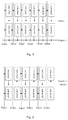
- FIG. 1 is a schematic view showing a conventional touch display module
- FIG. 2 is a schematic view showing a touch display module according to at least one embodiment of the present disclosure
- FIG. 3 is a schematic view showing a pixel unit included in the touch display module according to at least one embodiment of the present disclosure
- FIG. 4 is a schematic view showing a double-pixel compensation circuit of the touch display module according to at least one embodiment of the present disclosure
- FIG. 5 is a circuit diagram of the double-pixel compensation circuit of the touch display module according to at least one embodiment of the present disclosure
- FIG. 6 is a time sequence diagram of the double-pixel compensation circuit in FIG. 5 ;
- FIG. 7A is a circuit diagram of the double-pixel compensation circuit in FIG. 5 at a resetting stage of each display time period;
- FIG. 7B is a circuit diagram of the double-pixel compensation circuit in FIG. 5 at a first charging stage of each display time period;
- FIG. 7C is a circuit diagram of the double-pixel compensation circuit in FIG. 5 at a second charging stage of each display time period;
- FIG. 7D is a circuit diagram of the double-pixel compensation circuit in FIG. 5 at a light-emitting stage of each display time period.
- FIG. 8 is a flow chart of a method for driving the touch display module according to at least one embodiment of the present disclosure.
- FIG. 9 is a schematic view showing touch electrodes in the touch display modules according to at least one embodiment of the present disclosure.
- pixel units in an upper row presents the pixel units in an n th row
- pixel units in a lower row represents the pixel units in an (n+1) th row
- n is a positive integer
- Data 1 , Data 2 , Data 3 , Data 4 , Data 5 and Data 6 represent a first data line, a second data line, a third data, a fourth data line, a fifth data line and a sixth data line
- Gate n represents an n th gate line
- Gate n+1 represents an (n+1) th gate line.
- the pixel units in a first column are connected to Data 1
- the pixel units in a second column are connected to Data 2
- the pixel units in a third column are connected to Data 3
- the pixel units in a fourth column are connected to Data 4
- the pixel units in a fifth column are connected to Data 5
- the pixel units in a sixth column are connected to Data 6
- the pixel units in an n th row are connected to Gate n
- the pixel units in an (n+1) th row are connected to Gate n+1.
- a single-pixel compensation circuit is adopted by the conventional touch display module, and it is necessary to provide a data line for the pixel units in each column, so as to provide a data line at a display time period.
- an additional via-hole and an additional touch scanning line need to be provided at a pixel region, so as to apply a touch scanning signal to a touch electrode at a touch time period. Due to this design, an aperture ratio of the pixel region may be reduced, and thereby a service life of a display panel may be adversely affected.
- a touch display module including touch electrodes, a plurality of pixel units arranged in rows and columns, a plurality of gate lines, and a plurality of data lines crossing the plurality of gate lines.
- the touch display module further includes a plurality of touch scanning lines.
- the pixel units in two columns are arranged between every two adjacent data lines, and each data line is electrically connected to the pixel units arranged in two columns and adjacent to the data line.
- each touch scanning line is arranged between two adjacent data lines and connected to the corresponding touch electrode.
- Two gate lines are arranged between every two adjacent rows of pixel units.
- the pixel units in each row include a first pixel unit and a second pixel unit arranged adjacent to each other.
- the gate lines include a first gate line and a second gate line.
- the first pixel unit and the second pixel unit are electrically connected to a same data line, the first pixel unit is connected to the first gate line, and the second pixel unit is connected to the second gate line.
- the first pixel unit and the second pixel unit are arranged in a same row and in two adjacent columns, and connected to different gate lines.
- the pixel units in two columns are arranged between every two adjacent data lines, and each data line is electrically connected to the pixel units arranged in two columns and adjacent to the data line.
- the touch scanning signal is applied to the touch electrode through the touch scanning line arranged between the two adjacent data lines.
- the touch scanning line is arranged between two adjacent columns of pixel units which are connected to different data lines.
- the touch scanning line is located between the pixel units arranged in two adjacent columns and connected to different data lines. A position of the touch scanning line will be described hereinafter in conjunction with the drawings.
- the touch scanning line extends in a direction same to the data line.
- the pixel units in two columns may be arranged between every two adjacent data lines, and each data line is connected to the pixel units arranged in two columns and adjacent to the data line, so as to use a remaining signal line as the touch scanning line, thereby to simplify the arrangement process of the touch scanning line and improve the aperture ratio.
- the touch display module further includes a touch driving unit connected to the touch scanning line and configured to output a touch scanning signal to the corresponding touch electrode via the touch scanning line at a touch time period.
- each display period includes a display time period and a touch time period.
- the touch driving unit of the touch display module is configured to output at the touch time period, the touch scanning signal to the touch electrode through the touch scanning line arranged between two adjacent data lines.
- the pixel units in an upper row represent the pixel units in an n th row
- the pixel units in a lower row represent the pixel units in an (n+1) th row
- n is a positive integer
- Data 1 , Data 2 and Data 3 represent a first data line, a second data line and a third data line respectively
- TPM 1 , TPM 2 and TPM 3 represent a first touch scanning line, a second touch scanning line and a third touch scanning line respectively.
- the pixel units in a first column are connected to Data 1
- the pixel units in a second column and a third column are connected to Data 2
- the pixel units in a fourth column and a fifth column are connected to Data 3 .
- TPM 1 is arranged between Data 1 and Data 2
- TPM 2 is arranged between Data 2 and Data 3
- TPM 3 is arranged between Data 3 and a fourth data line (not shown).
- the data signal is applied to the pixel units through Data 1 , Data 2 and Data 3 connected thereto
- the touch scanning signal is applied to the touch electrodes through TPM 1 , TPM 2 and TPM 3 connected thereto.
- Gate 2 n ⁇ 1 represents a (2n ⁇ 1) th gate line
- Gate 2 n represents a (2n) th gate line.
- Gate 2 n ⁇ 1 and Gate 2 n are arranged between the n th -row pixel units and the (n+1) th -row pixel units.
- the pixel unit in the n th row and the first column is connected to Gate 2 n
- the pixel unit in the n th row and the second column is connected to Gate 2 n ⁇ 1
- the pixel unit in the n th row and the third column is connected to Gate 2 n
- the pixel unit in the n th row and the fourth column is connected to Gate 2 n ⁇ 1
- the pixel unit in the n th row and the fifth column is connected to Gate 2 n
- the pixel unit in the n th row and the sixth column is connected to Gate 2 n ⁇ 1.
- Gate 2 n and Gate 2 n ⁇ 1 are configured to enable, at the display time period, the pixel unit in the n th row and the second column and the pixel unit in the n th row and the third column to receive the data signal from Data 2 in a time-division manner, and enable, at the display time period, the pixel unit in the n th row and the fourth column and the pixel unit in the n th row and the fifth column to receive the data signal from Data 3 in a time-division manner.
- the data signal is not applied to the pixel units in two columns through one data line, so the number of the data lines is twice than that in FIG. 2 , i.e., in the related art, the data line is located at a position where the touch scanning line is located in FIG. 2 . Additional touch scanning lines need to be provided even in the case of more data lines, so an aperture ratio is too small.
- the double-pixel compensation circuit i.e., through the application of the data signal to the pixel units in two columns via one data line, it is able to provide the touch scanning line between two data lines, thereby to improve the aperture ratio.
- the touch display module further includes a plurality of cathodic electrodes which are also used as the touch electrodes, and the touch driving unit is further configured to output the touch scanning signal to the corresponding cathodic electrode via the touch scanning line at the touch time period.
- each cathodic electrode is arranged above a plurality of pixel units.
- the uppermost cathodic electrode may be divided and multiplexed, i.e., the cathodic electrode as an entire layer may be divided into a plurality of block-like cathodic electrodes with respect to each pixel region, and each block-like cathodic electrode may serve as a touch electrode at the touch time period.
- the touch scanning signal may be applied to the plurality of block-like cathodic electrodes through the touch scanning line at the touch time period.
- a via-hole and a TPM (touch electrode) line may be arranged at the pixel region. Due to this design, the aperture ratio of the pixel region may be reduced, and thereby a service life of the OLED may be adversely affected.
- each pixel unit includes an OLED and a pixel driver circuit connected to each other.
- the pixel driver circuit is configured to enable, at the touch time period, an anode of the corresponding OLED to be in a floating state, so as to enable the OLED not to emit light.
- a capacitance between a cathode and the anode may be omitted, so it is able to remarkably reduce RC loading, thereby to increase a touch driving frequency.
- the pixel driver circuit is further connected to a light-emission control line.
- the touch driving unit is further connected to the light-emission control line and further configured to output a light-emission turn-off control signal to the light-emission control line at the touch time period, so as to enable an anode of the corresponding OLED to be in a floating state under the control of the pixel driver circuit.
- this black frame insertion mode i.e., a mode where no power is applied to the anode
- the anode of the OLED may be equivalently in the floating state at the touch time period.
- the touch driving unit is further configured to output, at the touch time period, the touch scanning signal to control lines connected to the pixel driver circuit other than the light-emission control line, and signal lines connected to the pixel driver circuit.
- the touch scanning signal is outputted not only to the touch electrode, but also to the control lines connected to the pixel driver circuit and arranged under the touch electrode (other than the light-emission control line) and the signal lines connected to the pixel driver circuit.
- the touch electrode, the control lines connected to the pixel driver circuit (other than the light-emission control line) and the signal lines connected to the pixel driver circuit may be driven synchronously, so as to cancel out the influence of a ground capacitor on the touch electrode.
- the touch display module includes a plurality of first pixel units, a plurality of second pixel units, a plurality of first gate lines and a plurality of second gate lines.
- each first pixel unit 31 includes a first OLED 1 and a first pixel driver circuit PD 1
- each second pixel unit 32 includes a second OLED 2 and a second pixel driver circuit PD 2
- a cathode of the OLED 1 and a cathode of the OLED 2 are both connected to a ground end GND.
- the first pixel unit 31 and the corresponding second pixel unit 32 are arranged in a same row and in adjacent columns, and an n th data line Data n is arranged between the first pixel unit 31 and the second pixel unit 32 , where n is a positive integer.
- Each first pixel driver circuit PD 1 is connected to one of the first gate lines G 1
- each second pixel driver circuit PD 2 is connected to one of the second gate lines G 2 .
- Each first pixel driver circuit PD 1 and the corresponding second pixel driver circuit PD 2 are connected to the n th data line Data n, so as to receive a data signal from the n th data line Data n in a time-division manner at the display time period.
- each first pixel driver circuit and the corresponding second pixel driver circuit are connected to a same light-emission control line
- Each first pixel driver circuit includes a first driving transistor DTFT 1 , a first storage capacitor Cs 1 , a first resetting module 311 , a first charging control module 312 and a first light-emission control module 313 .
- Each second pixel driver circuit includes a second driving transistor DTFT 2 , a second storage capacitor Cs 2 , a second resetting module 321 , a second charging control module 322 and a second light-emission control module 323 .
- a gate electrode of the first driving transistor DTFT 1 is connected to the first resetting module 311 , a first electrode thereof is connected to a first level line through the first light-emission control module 313 and further connected to the gate electrode of the first driving transistor DTFT 1 through the first charging control module 312 , and a second electrode thereof is connected to an anode of the first OLED 1 through the first light-emission control module 313 and further connected to the nth data line Data n through the first charging control module 312 .
- a first end of the first storage capacitor Cs 1 is connected to the gate electrode of the first driving transistor DTFT 1 , and a second end thereof is connected to the first level line.
- the first level line is configured to receive a first level V 1 .
- a gate electrode of the second driving transistor DTFT 2 is connected to the second resetting module 321 , a first electrode thereof is configured to receive the first level V 1 through the second light-emission control module 323 and connected to the gate electrode of the second driving transistor DTFT 2 through the second charging control module 322 , and a second electrode thereof is connected to an anode of the second OLED 2 through the second light-emission control module 323 and further connected to the nth data line Data n through the second charging control module 322 .
- a first end of the second storage capacitor Cs 2 is connected to the gate electrode of the second driving transistor DTFT 2 , and a second end of the second storage capacitor Cs 2 is connected the first level line.
- the first resetting module 311 is connected to a resetting scanning line RS and a resetting signal line S 1 , and configured to, at a resetting stage of each display time period, reset a potential at the gate electrode of the first driving transistor DTFT 1 to a resetting voltage on the resetting signal line S 1 under the control of a first scanning signal from the resetting scanning line RS, so as to turn off the first driving transistor DTFT 1 .
- the second resetting module 321 is connected to the resetting scanning line RS and the resetting signal line S 1 , and configured to, at the resetting stage of each display time period, reset a potential at the gate electrode of the second driving transistor DTFT 2 to the resetting voltage on the resetting signal line S 1 under the control of the first scanning signal from the resetting scanning line RS, so as to turn off the second driving transistor DTFT 2 .
- the first charging control module 312 is connected to the first gate line G 1 and the n th data line Data n, and configured to, at a first charging stage of each display time period, enable the first electrode of the first driving transistor DTFT 1 to be connected to the gate electrode of the first driving transistor DTFT 1 and enable the second electrode of the first driving transistor DTFT 1 to receive a first data voltage Vdata 1 on the n th data line Data n under the control of a second scanning signal from the first gate line G 1 , so as to turn on the first driving transistor DTFT 1 , thereby to enable the first data voltage Vdata 1 to charge the first storage capacitor Cs 1 through the first driving transistor DTFT 1 until the potential at the gate electrode of the first driving transistor DTFT 1 is equal to Vdata 1 ⁇ Vth 1 , where Vth 1 represents a threshold voltage of the first driving transistor DTFT 1 .
- the second charging control module 322 is connected to the second gate line G 2 and the n th data line Data n, and configured to, at a second charging stage of each display time period, enable the first electrode of the second driving transistor DTFT 2 to be connected to the gate electrode of the second driving transistor DTFT 2 and enable the second electrode of the second driving transistor DTFT 2 to receive a second data voltage Vdata 2 on the n th data line Data n under the control of a third scanning signal from the second gate line G 2 , so as to turn on the second driving transistor DTFT 2 , thereby to enable the second data voltage Vdata 2 to charge the second storage capacitor Cs 2 through the second driving transistor DTFT 2 until the potential at the gate electrode of the second driving transistor DTFT 2 is equal to Vdata 2 ⁇ Vth 2 , where Vth 2 represents a threshold voltage of the second driving transistor DTFT 2 .
- the first light-emission control module 313 is connected to the light-emission control line EM and the first level line, and configured to, at a light-emitting stage of each display time period, enable the first electrode of the first driving transistor DTFT 1 to be connected to the first level line and enable the second electrode of the first driving transistor DTFT 1 to be connected to the anode of the first OLED 1 under the control of the light-emission control line EM, so as to enable the first driving transistor DTFT 1 to drive the first OLED 1 to emit light.
- the second light-emission control module 323 is connected to the light-emission control line EM and the first level line, and configured to, at the light-emitting stage of each display time period, enable the first electrode of the second driving transistor DTFT 2 to be connected to the first level line and enable the second electrode of the second driving transistor DTFT 2 to be connected to the anode of the second OLED 2 under the control of the light-emission control line EM, so as to enable the second driving transistor DTFT 2 to drive the second OLED 2 to emit light.
- the first level line is configured to receive the first level V 1 .
- the resetting signal line S 1 may be a common electrode line for outputting a common voltage Vcom, or a ground line.
- DTFT 1 and DTFT 2 may be p-type TFTs, and in actual operation, they may also be n-type TFTs.
- the first charging control module 312 may be configured to enable the first data voltage Vdata 1 to charge the first storage capacitor Cs 1 through the first driving transistor DTFT 1 under the control of the second scanning signal from the first gate line G 1 .
- the second charging control module 322 may be configured to enable the second electrode of the second driving transistor DTFT 2 to receive the second data voltage Vdata 2 on the n th data line Data n under the control of the third scanning signal from the second gate line G 2 , so as to turn on the second driving transistor DTFT 2 , thereby to enable the second data voltage Vdata 2 to charge the second storage capacitor Cs 2 through the second driving transistor DTFT 2 .
- the transistors may be thin film transistors, field effect transistors or any other elements having a same characteristic.
- a first electrode of the transistor may be a source electrode or a drain electrode
- a second electrode may be a drain electrode or a source electrode.
- the transmission may be an n-type or a p-type transistor.
- all the transistors are p-type transistors.
- p-type transistors may also be used, which all falls within the scope of the present disclosure.
- the touch driving unit is further configured to, at the touch time period, output a light-emission turn-off control signal to the light-emission control line, so as to enable the anode of the first OLED to be in the floating state under the control of the first pixel driver circuit and thereby to enable the first OLED not to emit light, and enable the anode of the second OLED to be in the floating state under the control of the second pixel driver circuit and thereby to enable the second OLED not to emit light.
- a capacitance between the cathode and the anode of the first OLED and a capacitance between the cathode and the anode of the second OLED may be omitted. As a result, it is able to remarkably reduce the RC loading, thereby to increase the touch driving frequency.
- the touch driving unit is further configured to, at the touch time period, output the touch scanning signal to the touch electrode, the data line, the resetting scanning line, the first gate line and the second gate line simultaneously, so as to drive the touch electrode, the data line, the resetting scanning line, the first gate line and the second gate line synchronously.
- the touch electrode, the control lines connected to the pixel driver circuit other than the light-emission control line, and the signal lines connected to the pixel driver circuit may be driven synchronously, so as to cancel out the influence of the ground capacitor on the touch electrode.
- the first resetting module includes a first resetting transistor, a gate electrode of which is connected to the resetting scanning line, a first electrode of which is connected to the gate electrode of the first driving transistor, and a second electrode of which is connected to the resetting signal line.
- the second resetting module includes a second resetting transistor, a gate electrode of which is connected to the resetting scanning line, a first electrode of which is connected to the gate electrode of the second driving transistor, and a second electrode of which is connected to the resetting signal line.
- the first charging control module includes: a first data inputting transistor, a gate electrode of which is connected to the first gate line, a first electrode of which is connected to the n th data line, and a second electrode of which is connected to the second electrode of the first driving transistor; and a first charging control transistor, a gate electrode of which is connected to the first gate line, a first electrode of which is connected to the gate electrode of the first driving transistor, and a second electrode of which is connected to the first electrode of the first driving transistor.
- the second charging control module includes: a second data inputting transistor, a gate electrode of which is connected to the second gate line, a first electrode of which is connected to the n th data line, and a second electrode of which is connected to the second electrode of the second driving transistor; and a second charging control transistor, a gate electrode of which is connected to the second gate line, a first electrode of which is connected to the gate electrode of the second driving transistor, and a second electrode of which is connected to the first electrode of the second driving transistor.
- the first light-emission control module includes: a first light-emission control transistor, a gate electrode of which is connected to the light-emission control line, a first electrode of which is connected to the first level line, and a second electrode of which is connected to the first electrode of the first driving transistor; and a second light-emission control transistor, a gate electrode of which is connected to the light-emission control line, a first electrode of which is connected to the second electrode of the first driving transistor, and a second electrode of which is connected to the anode of the first OLED.
- the second light-emission control module includes: a third light-emission control transistor, a gate electrode of which is connected to the light-emission control line, a first electrode of which is connected to the first level line, and a second electrode of which is connected to the first electrode of the second driving transistor; and a fourth light-emission control transistor, a gate electrode of which is connected to the light-emission control line, a first electrode of which is connected to the second electrode of the second driving transistor, and a second electrode of which is connected to the anode of the second OLED.
- the double-pixel compensation circuit of the touch display module will be described hereinafter in more details.
- the first pixel driver circuit includes the first driving transistor DTFT 1 , the first storage capacitor Cs 1 , the first resetting module, the first charging control module and the first light-emission control module.
- the second pixel driver circuit includes the second driving transistor DTFT 2 , the second storage capacitor Cs 2 , the second resetting module, the second charging control module and the second light-emission control module.
- the first resetting module includes a first resetting transistor T 11 , a gate electrode of which is configured to receive a first scanning signal Scan 1 , a source electrode of which is connected to the gate electrode of the first driving transistor DTFT, and a drain electrode of which is grounded.
- the second resetting module includes a second resetting transistor T 21 , a gate electrode of which is configured to receive the first scanning signal Scan 1 , a first electrode of which is connected to the gate electrode of the second driving transistor DTFT 2 , and a second electrode of which is grounded.
- the first charging control module includes: a first data inputting transistor T 12 , a gate electrode of which is configured to receive a second scanning signal Scan 2 , a source electrode of which is connected to the n th data line Data n, and a drain electrode of which is connected to a drain electrode of the first driving transistor DTFT 1 ; and a first charging control transistor T 13 , a gate electrode of which is configured to receive the second scanning signal Scan 2 , a source electrode of which is connected to the gate electrode of the first driving transistor DTFT 1 , and a drain electrode of which is connected to a source electrode of the first driving transistor DTFT 1 .
- the first light-emission control module includes: a first light-emission control transistor T 14 , a gate electrode of which is connected to the light-emission control line EM, a source electrode of which is configured to receive a high level VDD, and a drain electrode of which is connected to the source electrode of the first driving transistor DTFT 1 ; and a second light-emission control transistor T 15 , a gate electrode of which is connected to the light-emission control line EM, a source electrode of which is connected to the drain electrode of the first driving transistor DTFT 1 , and a drain electrode of which is connected to the anode of the first OLED 1 .
- the second charging control module includes: a second data inputting transistor T 22 , a gate electrode of which is configured to receive a third scanning signal Scan 3 , a source electrode of which is connected to the n th data line Data n, and a drain electrode of which is connected to a drain electrode of the second driving transistor DTFT 2 ; and a second charging control transistor T 23 , a gate electrode of which is configured to receive the third scanning signal Scan 3 , a source electrode of which is connected to the gate electrode of the second driving transistor DTFT 2 , and a drain electrode of which is connected to a source electrode of the second driving transistor DTFT 2 .
- the second light-emission control module includes: a third light-emission control transistor T 24 , a gate electrode of which is connected to the light-emission control line EM, a source electrode of which is configured to receive the high level VDD, and a drain electrode of which is connected to the source electrode of the second driving transistor DTFT 2 ; and a fourth light-emission control transistor T 25 , a gate electrode of which is connected to the light-emission control line EM, a source electrode of which is connected to the drain electrode of the second driving transistor DTFT 2 , and a drain electrode of which is connected to the anode of the second OLED 2 .
- a first end a 1 of the first storage capacitor Cs 1 is connected to the gate electrode of the DTFT 1 , and a second end b 1 thereof is configured to receive VDD.
- a first end a 2 of the second storage capacitor Cs 2 is connected to the gate electrode of the DTFT 2 , and a second end b 2 thereof is configured to receive VDD.
- all the transistors are p-type TFTs.
- FIG. 6 shows a time sequence diagram of the driver circuit in FIG. 5 .
- S 1 represents the resetting stage of each display time period
- S 2 represents the first charging stage of each display time period
- S 3 represents the second charging stage of each display time period
- S 4 represents the light-emitting stage of each display time period
- S 5 represents the touch time period.
- T 12 and T 13 are turned on, and T 22 , T 23 , T 11 , T 14 , T 15 , T 21 , T 24 and T 25 are turned off. Because a 1 and a 2 have been grounded, DTFT 1 may be turned on, and a 1 may be charged by the first data voltage Vdata 1 on Data n through T 12 , DTFT 1 and T 13 , until the potential at a 1 is equal to Vdata 1 ⁇ Vth 1 (i.e., a gate-to-source voltage of DTFT 1 is equal to the threshold voltage Vth 1 of DTFT 1 ).
- the potential at b 1 may be maintained at Vdata 1 ⁇ Vth 1 after the charging procedure.
- T 15 is turned off, so no current may flow through OLED 1 , i.e., it is able to indirectly prolong a service life of OLED 1 .
- T 22 and T 23 are turned on, and T 12 , T 13 , T 11 , T 14 , T 15 , T 21 , T 24 and T 25 are turned off. Because a 1 and a 2 have been grounded, DTFT 2 may be turned on, and a 2 may be charged by the second data voltage Vdata 2 on Data n through T 22 , DTFT 2 and T 23 , until the potential at a 2 is equal to Vdata 2 ⁇ Vth 2 (i.e., a gate-to-source voltage of DTFT 2 is equal to the threshold voltage Vth 2 of DTFT 2 ).
- the potential at b 2 may be maintained at Vdata 2 ⁇ Vth 2 after the charging procedure.
- T 25 is turned off, so no current may flow through OLED 2 , i.e., it is able to indirectly prolong a service life of OLED 2 .
- the source electrode of DTFT 1 and the source electrode DTFT 2 are configured to receive VDD.
- the current flows through T 14 , DTFT 1 and T 15 , so as to enable OLED 1 to emit light, and the current flows through T 24 , DTFT 2 and T 25 , so as to enable OLED 2 to emit light.
- K 1 represents a current amplification coefficient of DTFT 1
- V GS1 represents a gate-to-source voltage of DTFT 1
- I OLED1 represents an operating current of OLED 1
- K 2 represents a current amplification coefficient of DTFT 2
- V GS2 represents a gate-to-source voltage of DTFT 2
- I OLED2 represents an operating current of OLED 2 .
- I OLED1 is relevant to VDD and Vdata 1 , rather than Vth 1
- I OLED2 is relevant to VDD and Vdata 2 , rather than Vth 2 .
- the signal lines other than the light-emission control line EM are driven synchronously, and an amplitude of the touch driving signal is smaller than a voltage amplitude on the signal lines at the display time period, so as to ensure all the TFTs to be kept in the initial states (i.e., in the states at the light-emitting stage of the display time period).
- no current flows through the anodes of OLED 1 and OLED 2 so OLED 1 and OLED 2 are each in the floating state. It is unnecessary to calculate a capacitance between the touch electrode and the anode, thereby to reduce the RC loading and effectively increase the driving frequency.
- the present disclosure provides in some embodiments a method for driving the above-mentioned touch display module, which includes: Step S 1 of, at a display time period, enabling pixel units arranged in two columns and electrically connected to a same data line to receive a data signal from the data line in a time-division manner; and Step S 2 of, at a touch time period, outputting a touch scanning signal to a touch electrode through a touch scanning line arranged between two adjacent data lines.
- the pixel units arranged in two columns and electrically connected to the same data line may receive the data signal from the data line in a time-division manner at the display time period, and the touch scanning signal may be applied to the touch electrode via the touch scanning line between the two adjacent data lines at the touch time period.
- the touch display module further includes a touch driving unit, and the step of outputting the touch scanning signal to the touch electrode through the touch scanning line arranged between the two adjacent data lines includes outputting, by the touch driving unit, the touch scanning signal to the touch electrode through the touch scanning line.
- the touch display module further includes a plurality of cathodic electrodes.
- the method further includes enabling the plurality of cathodic electrodes of the touch display module to be also used as the touch electrodes.
- the step of outputting, by the touch driving unit, the touch scanning signal to the touch electrode through the touch scanning line includes outputting, by the touch driving unit, the touch scanning signal to the cathodic electrode though the touch scanning line.
- the uppermost cathodic electrode may be divided and multiplexed, i.e., the cathodic electrode as an entire layer may be divided into a plurality of block-like cathodic electrodes corresponding to each pixel region, and each block-like cathodic electrode may serve as one touch electrode at the touch time period.
- the touch scanning signal may be applied to the plurality of block-like cathodic electrodes via the touch scanning line at the touch time period.
- the pixel units in each column include a plurality of subpixel units each includes an OLED and a pixel driver circuit.
- the method further includes, at the touch time period, enabling, by the pixel driver circuit, an anode of the corresponding OLED to be in a floating state, so as to enable the OLED not to emit light.
- the anode of the corresponding OLED may be in the floating state under the control of the pixel driver circuit, so as to enable the OLED not to emit light.
- the capacitance between the cathode and the anode may be omitted, so it is able to remarkably reduce the RC loading, thereby to increase the touch driving frequency.
- the step of enabling, by the pixel driver circuit, the anode of the corresponding OLED to be in the floating state includes outputting, by the touch driving unit, a light-emission turn-off control signal to the light-emission control line, so as to enable the anode of the corresponding OLED to be in the floating state under the control of the pixel driver circuit.
- the touch display module includes a plurality of first pixel units, a plurality of second pixel units, a plurality of first gate lines and a plurality of second gate lines.
- Each first pixel unit includes a first OLED and a first pixel driver circuit
- each second pixel unit includes a second OLED and a second pixel driver circuit.
- the first pixel unit and the corresponding second pixel unit are arranged in a same row and in adjacent columns, and an n th data line is arranged between the first pixel unit and the second pixel unit, where n is a positive integer.
- Each first pixel driver circuit is connected to one of the first gate lines
- each second pixel driver circuit is connected to one of the second gate lines.
- Each first pixel driver circuit and the corresponding second pixel driver circuit are connected to the n th data line.
- the step of enabling, at the display time period, the pixel units arranged in two columns and electrically connected to the same data line to receive the data signal from the data line in a time-division manner includes enabling, at the display time period, the first pixel driver circuit and the second pixel driver circuit to receive a data signal from the n th data line in a time-division manner.
- each first pixel driver circuit and the corresponding second pixel driver circuit are connected to a same light-emission control line.
- Each first pixel driver circuit includes a first driving transistor, a first storage capacitor, a first resetting module, a first charging control module and a first light-emission control module.
- Each second pixel driver circuit includes a second driving transistor, a second storage capacitor, a second resetting module, a second charging control module and a second light-emission control module.
- the display time period includes a resetting stage, a first charging stage, a second charging stage and a light-emitting stage.
- the step of enabling, at the display time period, the first pixel driver circuit and the second pixel driver circuit to receive the data signal from the n th data line in a time-division manner includes: at the resetting stage of each display time period, resetting, by the first resetting module, a potential at a gate electrode of the first driving transistor to a resetting voltage on the resetting signal line under the control of a first scanning signal from the resetting scanning line so as to turn off the first driving transistor, and resetting, by the second resetting module, a potential at a gate electrode of the second driving transistor to the resetting voltage on the resetting signal line under the control of the first scanning signal from the resetting scanning line so as to turn off the second driving transistor; at the first charging stage of each display time period, enabling, by the first charging control module, a first electrode of the first driving transistor to be electrically connected to the gate electrode of the first driving transistor and enabling a second electrode of the first driving transistor to receive a first data voltage V
- the method further includes, at the touch time period, outputting, by the touch driving unit, the touch scanning signal to the touch electrode, the data line, the resetting scanning line, the first gate line and the second gate line, so as to drive the touch electrode, the data line, the resetting scanning line, the first gate line and the second gate line synchronously.
- the touch electrode, the control lines connected to the pixel driver circuit other than the light-emission control line and the signal lines connected to the pixel driver circuit may be driven synchronously, so as to cancel out the influence of the ground capacitor on the touch electrode.
- the present disclosure further provides in some embodiments a touch display panel including the above-mentioned touch display module.
- the present disclosure further provides in some embodiments a touch display device including the above-mentioned touch display panel.
Landscapes
- Engineering & Computer Science (AREA)
- Theoretical Computer Science (AREA)
- Physics & Mathematics (AREA)
- General Physics & Mathematics (AREA)
- General Engineering & Computer Science (AREA)
- Computer Hardware Design (AREA)
- Human Computer Interaction (AREA)
- Control Of El Displays (AREA)
- Control Of Indicators Other Than Cathode Ray Tubes (AREA)
- Electroluminescent Light Sources (AREA)
Abstract
Description
Claims (16)
Applications Claiming Priority (4)
| Application Number | Priority Date | Filing Date | Title |
|---|---|---|---|
| CN201610221874.9A CN105679251B (en) | 2016-04-11 | 2016-04-11 | Touch-control display module and its driving method, touch-control display panel and device |
| CN201610221874.9 | 2016-04-11 | ||
| CN201610221874 | 2016-04-11 | ||
| PCT/CN2017/070226 WO2017177730A1 (en) | 2016-04-11 | 2017-01-05 | Touch control display module, driving method therefor, touch control display panel, and device |
Publications (2)
| Publication Number | Publication Date |
|---|---|
| US20190025965A1 US20190025965A1 (en) | 2019-01-24 |
| US10545592B2 true US10545592B2 (en) | 2020-01-28 |
Family
ID=56310210
Family Applications (1)
| Application Number | Title | Priority Date | Filing Date |
|---|---|---|---|
| US15/554,173 Active US10545592B2 (en) | 2016-04-11 | 2017-01-05 | Touch display module, method for driving the same, touch display panel and touch display device |
Country Status (4)
| Country | Link |
|---|---|
| US (1) | US10545592B2 (en) |
| EP (1) | EP3444800A4 (en) |
| CN (1) | CN105679251B (en) |
| WO (1) | WO2017177730A1 (en) |
Cited By (1)
| Publication number | Priority date | Publication date | Assignee | Title |
|---|---|---|---|---|
| US11276355B2 (en) * | 2020-02-10 | 2022-03-15 | Silicon Works Co., Ltd. | Timing controller for controlling emission of emission element for recognizing touch coordinates and electronic device including the same |
Families Citing this family (30)
| Publication number | Priority date | Publication date | Assignee | Title |
|---|---|---|---|---|
| CN105679251B (en) | 2016-04-11 | 2018-11-30 | 京东方科技集团股份有限公司 | Touch-control display module and its driving method, touch-control display panel and device |
| CN106782310B (en) * | 2017-03-01 | 2019-09-03 | 上海天马有机发光显示技术有限公司 | Pixel circuit, driving method, display panel and display device |
| CN107092388B (en) * | 2017-04-12 | 2024-05-03 | 北京集创北方科技股份有限公司 | Touch display device and driving method thereof |
| CN106908980B (en) * | 2017-05-09 | 2020-10-16 | 上海中航光电子有限公司 | Array substrate, touch display panel and display device |
| CN108874195A (en) | 2017-05-12 | 2018-11-23 | 京东方科技集团股份有限公司 | Touch pixel-driving circuit and driving method, touch control display apparatus |
| CN109254677A (en) * | 2017-07-13 | 2019-01-22 | 群创光电股份有限公司 | Display device and method for sensing touch signal using the same |
| CN107230455A (en) * | 2017-07-21 | 2017-10-03 | 京东方科技集团股份有限公司 | A kind of pixel-driving circuit, image element driving method and display base plate |
| CN109558024B (en) * | 2017-09-27 | 2024-05-17 | 京东方科技集团股份有限公司 | Display device, touch panel, manufacturing method of touch panel and driving method of touch panel |
| CN108628047B (en) * | 2018-04-02 | 2021-07-30 | 上海中航光电子有限公司 | Array substrate, display panel and display device |
| CN108536336B (en) | 2018-04-24 | 2020-04-17 | 京东方科技集团股份有限公司 | Touch circuit and touch driving method |
| CN108447441B (en) * | 2018-05-10 | 2019-10-11 | 京东方科技集团股份有限公司 | Pixel circuit, driving method thereof, display substrate, display device |
| CN108682377A (en) * | 2018-05-16 | 2018-10-19 | 京东方科技集团股份有限公司 | display module and its driving method, display panel and device |
| CN110211539B (en) * | 2018-08-02 | 2021-04-27 | 京东方科技集团股份有限公司 | Pixel driving circuit, pixel driving method and touch display device |
| CN109189269B (en) * | 2018-09-12 | 2020-08-04 | 南京中电熊猫平板显示科技有限公司 | Display panel and driving method thereof |
| CN109521593B (en) * | 2018-12-25 | 2021-07-09 | 厦门天马微电子有限公司 | Display panel and display device |
| CN109545162A (en) * | 2018-12-29 | 2019-03-29 | 上海中航光电子有限公司 | Array substrate and its driving method, display panel and display device |
| CN110197643B (en) * | 2019-07-05 | 2021-03-30 | 京东方科技集团股份有限公司 | Pixel drive circuit and display device |
| CN210155492U (en) * | 2019-08-16 | 2020-03-17 | 北京京东方显示技术有限公司 | Array substrate and display device |
| CN110675826A (en) * | 2019-10-21 | 2020-01-10 | 京东方科技集团股份有限公司 | Display panel, driving method thereof and display device |
| CN112820236B (en) * | 2019-10-30 | 2022-04-12 | 京东方科技集团股份有限公司 | Pixel driving circuit and driving method thereof, display panel, and display device |
| CN110956929A (en) * | 2020-01-02 | 2020-04-03 | 京东方科技集团股份有限公司 | Pixel driving circuit, driving method thereof, array substrate and display device |
| CN111063301B (en) * | 2020-01-09 | 2024-04-12 | 京东方科技集团股份有限公司 | Pixel circuit, driving method thereof, array substrate and display device |
| US11392246B2 (en) | 2020-05-07 | 2022-07-19 | Novatek Microelectronics Corp. | Method for driving touch-and-display device, driving circuit, and touch-and-display device |
| US11609657B2 (en) | 2020-05-07 | 2023-03-21 | Novatek Microelectronics Corp. | Method for driving touch-and-display device, driving circuit, and touch-and-display device |
| KR102832240B1 (en) * | 2020-07-27 | 2025-07-10 | 엘지디스플레이 주식회사 | Electroluminescence Display Device |
| CN115713918A (en) * | 2021-08-20 | 2023-02-24 | 京东方科技集团股份有限公司 | Display substrate and display device |
| US11568816B1 (en) * | 2022-02-03 | 2023-01-31 | Meta Platforms Technologies, Llc | Burn-in compensation scheme for light-emitting diode based displays |
| US11568813B1 (en) | 2022-05-10 | 2023-01-31 | Meta Platforms Technologies, Llc | Pixel level burn-in compensation for light-emitting diode based displays |
| CN115731873B (en) * | 2022-11-24 | 2025-03-25 | 合肥维信诺科技有限公司 | A display panel driving method, device and display device |
| CN120877659A (en) * | 2024-04-30 | 2025-10-31 | 合肥维信诺科技有限公司 | Display panel, driving method thereof, driving time sequence and display device |
Citations (18)
| Publication number | Priority date | Publication date | Assignee | Title |
|---|---|---|---|---|
| JP2010091608A (en) | 2008-10-03 | 2010-04-22 | Toshiba Mobile Display Co Ltd | Active matrix type display apparatus, and method of driving active matrix type display apparatus |
| US20100156954A1 (en) * | 2008-12-24 | 2010-06-24 | Samsung Electronics Co., Ltd. | Display apparatus |
| CN101989399A (en) | 2009-08-06 | 2011-03-23 | 深圳华映显示科技有限公司 | Display panel, driving method thereof and display device |
| CN102314248A (en) | 2010-06-29 | 2012-01-11 | 瀚宇彩晶股份有限公司 | Touch panel and pixel array thereof |
| US20120161140A1 (en) | 2010-12-22 | 2012-06-28 | Beijing Boe Optoelectronics Technology Co., Ltd. | Tft array substrate and manufacturing method thereof |
| CN102841718A (en) | 2012-08-31 | 2012-12-26 | 北京京东方光电科技有限公司 | Capacitance-type embedded touch screen and display device |
| CN103412676A (en) | 2013-07-29 | 2013-11-27 | 合肥京东方光电科技有限公司 | Touch screen and display device. |
| US20140111473A1 (en) * | 2012-10-19 | 2014-04-24 | Beijing Boe Optoelectronics Technology Co., Ltd. | Capacitive in cell touch panel and driving method thereof, display device |
| CN103760703A (en) | 2013-12-30 | 2014-04-30 | 深圳市华星光电技术有限公司 | Embedded touch device of double-gate panel |
| CN104091559A (en) | 2014-06-19 | 2014-10-08 | 京东方科技集团股份有限公司 | Pixel circuit as well as driving method and display device thereof |
| CN104091820A (en) | 2014-07-10 | 2014-10-08 | 京东方科技集团股份有限公司 | Pixel circuit and display device |
| CN104850270A (en) | 2015-06-11 | 2015-08-19 | 京东方科技集团股份有限公司 | Driving method and driving circuit of touch control module set, touch control module set, panel and device |
| CN104951143A (en) | 2015-07-27 | 2015-09-30 | 京东方科技集团股份有限公司 | Array substrate, touch panel and display device |
| CN204945586U (en) | 2015-09-28 | 2016-01-06 | 鄂尔多斯市源盛光电有限责任公司 | A kind of array base palte, In-cell touch panel and display device |
| US20160019827A1 (en) * | 2014-07-16 | 2016-01-21 | Lg Display Co., Ltd. | In-Cell Touch Display Device |
| CN105679251A (en) | 2016-04-11 | 2016-06-15 | 京东方科技集团股份有限公司 | Touch control display module group, driving method thereof, and touch control display panel and device |
| CN205507290U (en) | 2016-04-11 | 2016-08-24 | 京东方科技集团股份有限公司 | Touch -control display module assembly, touch -control display panel and device |
| US20170031487A1 (en) | 2015-07-27 | 2017-02-02 | Boe Technology Group Co., Ltd | Array substrate, touch panel and display apparatus containing the same |
-
2016
- 2016-04-11 CN CN201610221874.9A patent/CN105679251B/en active Active
-
2017
- 2017-01-05 US US15/554,173 patent/US10545592B2/en active Active
- 2017-01-05 EP EP17754057.2A patent/EP3444800A4/en not_active Withdrawn
- 2017-01-05 WO PCT/CN2017/070226 patent/WO2017177730A1/en not_active Ceased
Patent Citations (23)
| Publication number | Priority date | Publication date | Assignee | Title |
|---|---|---|---|---|
| JP2010091608A (en) | 2008-10-03 | 2010-04-22 | Toshiba Mobile Display Co Ltd | Active matrix type display apparatus, and method of driving active matrix type display apparatus |
| US20100156954A1 (en) * | 2008-12-24 | 2010-06-24 | Samsung Electronics Co., Ltd. | Display apparatus |
| CN101989399A (en) | 2009-08-06 | 2011-03-23 | 深圳华映显示科技有限公司 | Display panel, driving method thereof and display device |
| CN102314248A (en) | 2010-06-29 | 2012-01-11 | 瀚宇彩晶股份有限公司 | Touch panel and pixel array thereof |
| US20120161140A1 (en) | 2010-12-22 | 2012-06-28 | Beijing Boe Optoelectronics Technology Co., Ltd. | Tft array substrate and manufacturing method thereof |
| CN102566166A (en) | 2010-12-22 | 2012-07-11 | 北京京东方光电科技有限公司 | Double-gate TFT (thin film transistor) substrate and production method thereof |
| CN102841718A (en) | 2012-08-31 | 2012-12-26 | 北京京东方光电科技有限公司 | Capacitance-type embedded touch screen and display device |
| US20140111473A1 (en) * | 2012-10-19 | 2014-04-24 | Beijing Boe Optoelectronics Technology Co., Ltd. | Capacitive in cell touch panel and driving method thereof, display device |
| CN103412676A (en) | 2013-07-29 | 2013-11-27 | 合肥京东方光电科技有限公司 | Touch screen and display device. |
| US20150205156A1 (en) | 2013-12-30 | 2015-07-23 | Shenzhen China Star Optoelectronics Technology Co., Ltd. | In-cell touch device for double-grid panel |
| CN103760703A (en) | 2013-12-30 | 2014-04-30 | 深圳市华星光电技术有限公司 | Embedded touch device of double-gate panel |
| CN104091559A (en) | 2014-06-19 | 2014-10-08 | 京东方科技集团股份有限公司 | Pixel circuit as well as driving method and display device thereof |
| US20160224157A1 (en) | 2014-06-19 | 2016-08-04 | Boe Technology Group Co., Ltd. | Pixel circuit, driving method thereof and display device |
| CN104091820A (en) | 2014-07-10 | 2014-10-08 | 京东方科技集团股份有限公司 | Pixel circuit and display device |
| US20160247447A1 (en) * | 2014-07-10 | 2016-08-25 | Boe Technology Group Co., Ltd. | Pixel circuit and display apparatus |
| US20160019827A1 (en) * | 2014-07-16 | 2016-01-21 | Lg Display Co., Ltd. | In-Cell Touch Display Device |
| CN104850270A (en) | 2015-06-11 | 2015-08-19 | 京东方科技集团股份有限公司 | Driving method and driving circuit of touch control module set, touch control module set, panel and device |
| US20170168646A1 (en) | 2015-06-11 | 2017-06-15 | Boe Technology Group Co., Ltd. | Driving method and driving circuit of touch control module, touch control module, touch control panel and touch control device |
| CN104951143A (en) | 2015-07-27 | 2015-09-30 | 京东方科技集团股份有限公司 | Array substrate, touch panel and display device |
| US20170031487A1 (en) | 2015-07-27 | 2017-02-02 | Boe Technology Group Co., Ltd | Array substrate, touch panel and display apparatus containing the same |
| CN204945586U (en) | 2015-09-28 | 2016-01-06 | 鄂尔多斯市源盛光电有限责任公司 | A kind of array base palte, In-cell touch panel and display device |
| CN105679251A (en) | 2016-04-11 | 2016-06-15 | 京东方科技集团股份有限公司 | Touch control display module group, driving method thereof, and touch control display panel and device |
| CN205507290U (en) | 2016-04-11 | 2016-08-24 | 京东方科技集团股份有限公司 | Touch -control display module assembly, touch -control display panel and device |
Non-Patent Citations (2)
| Title |
|---|
| First Office Action for Chinese Application No. 201610221874.9, dated Oct. 11, 2017, 8 Pages. |
| International Search Report and Written Opinion for Application No. PCT/CN2017/070226, dated Mar. 29, 2017, 11 Pages. |
Cited By (1)
| Publication number | Priority date | Publication date | Assignee | Title |
|---|---|---|---|---|
| US11276355B2 (en) * | 2020-02-10 | 2022-03-15 | Silicon Works Co., Ltd. | Timing controller for controlling emission of emission element for recognizing touch coordinates and electronic device including the same |
Also Published As
| Publication number | Publication date |
|---|---|
| CN105679251A (en) | 2016-06-15 |
| US20190025965A1 (en) | 2019-01-24 |
| WO2017177730A1 (en) | 2017-10-19 |
| CN105679251B (en) | 2018-11-30 |
| EP3444800A4 (en) | 2019-10-09 |
| EP3444800A1 (en) | 2019-02-20 |
Similar Documents
| Publication | Publication Date | Title |
|---|---|---|
| US10545592B2 (en) | Touch display module, method for driving the same, touch display panel and touch display device | |
| US11881164B2 (en) | Pixel circuit and driving method thereof, and display panel | |
| US9886906B2 (en) | Pixel circuit, pixel circuit driving method and display device | |
| EP3200178B1 (en) | Pixel driver circuit, method, display panel, and display device | |
| US10032415B2 (en) | Pixel circuit and driving method thereof, display device | |
| US9852685B2 (en) | Pixel circuit and driving method thereof, display apparatus | |
| US9898960B2 (en) | Pixel circuit, its driving method, OLED display panel and OLED display device | |
| US9875690B2 (en) | Pixel circuit, display substrate and display panel | |
| US10504440B2 (en) | Pixel circuit, driving method thereof, display panel and display apparatus | |
| US9773451B2 (en) | Pixel circuit, method for driving pixel circuit and display apparatus | |
| CN102388414B (en) | Display device and method for driving same | |
| TWI567714B (en) | Display device | |
| US9548024B2 (en) | Pixel driving circuit, driving method thereof and display apparatus | |
| US20190340979A1 (en) | Pixel driving circuit, method for driving the same and display device | |
| US9984622B2 (en) | Pixel driving circuit, driving method thereof and display device using the same | |
| US20140118328A1 (en) | Pixel driving circuit of an active-matrix organic light-emitting diode and a method of driving the same | |
| US20180211599A1 (en) | Pixel circuit, driving method for the same and an organic light-emitting display | |
| CN104240634B (en) | Pixel structure and display device | |
| KR101507259B1 (en) | Image display device | |
| US9437142B2 (en) | Pixel circuit and display apparatus | |
| CN104167173A (en) | Pixel circuit for active organic light-emitting diode displayer | |
| US20180096654A1 (en) | Pixel circuit, display panel and display device | |
| CN107393478A (en) | Pixel internal compensation circuit and driving method | |
| US20190259335A1 (en) | Pixel driving circuitry and method for driving the same, display substrate and display device | |
| US20200219445A1 (en) | Pixel circuit, display panel, display apparatus and driving method |
Legal Events
| Date | Code | Title | Description |
|---|---|---|---|
| FEPP | Fee payment procedure |
Free format text: ENTITY STATUS SET TO UNDISCOUNTED (ORIGINAL EVENT CODE: BIG.); ENTITY STATUS OF PATENT OWNER: LARGE ENTITY |
|
| AS | Assignment |
Owner name: BEIJING BOE OPTOELECTRONICS TECHNOLOGY CO., LTD., CHINA Free format text: ASSIGNMENT OF ASSIGNORS INTEREST;ASSIGNORS:YANG, SHENGJI;DONG, XUE;XUE, HAILIN;AND OTHERS;REEL/FRAME:043475/0891 Effective date: 20170628 Owner name: BEIJING BOE OPTOELECTRONICS TECHNOLOGY CO., LTD., Free format text: ASSIGNMENT OF ASSIGNORS INTEREST;ASSIGNORS:YANG, SHENGJI;DONG, XUE;XUE, HAILIN;AND OTHERS;REEL/FRAME:043475/0891 Effective date: 20170628 Owner name: BOE TECHNOLOGY GROUP CO., LTD., CHINA Free format text: ASSIGNMENT OF ASSIGNORS INTEREST;ASSIGNORS:YANG, SHENGJI;DONG, XUE;XUE, HAILIN;AND OTHERS;REEL/FRAME:043475/0891 Effective date: 20170628 |
|
| STPP | Information on status: patent application and granting procedure in general |
Free format text: DOCKETED NEW CASE - READY FOR EXAMINATION |
|
| STPP | Information on status: patent application and granting procedure in general |
Free format text: NON FINAL ACTION MAILED |
|
| STPP | Information on status: patent application and granting procedure in general |
Free format text: RESPONSE TO NON-FINAL OFFICE ACTION ENTERED AND FORWARDED TO EXAMINER |
|
| STPP | Information on status: patent application and granting procedure in general |
Free format text: NOTICE OF ALLOWANCE MAILED -- APPLICATION RECEIVED IN OFFICE OF PUBLICATIONS |
|
| STPP | Information on status: patent application and granting procedure in general |
Free format text: PUBLICATIONS -- ISSUE FEE PAYMENT RECEIVED |
|
| STCF | Information on status: patent grant |
Free format text: PATENTED CASE |
|
| MAFP | Maintenance fee payment |
Free format text: PAYMENT OF MAINTENANCE FEE, 4TH YEAR, LARGE ENTITY (ORIGINAL EVENT CODE: M1551); ENTITY STATUS OF PATENT OWNER: LARGE ENTITY Year of fee payment: 4 |