US10522764B2 - Compound, light-emitting element comprising same and electronic device comprising the light-emitting element - Google Patents

Compound, light-emitting element comprising same and electronic device comprising the light-emitting element Download PDF

Info

Publication number
US10522764B2
US10522764B2 US14/420,582 US201314420582A US10522764B2 US 10522764 B2 US10522764 B2 US 10522764B2 US 201314420582 A US201314420582 A US 201314420582A US 10522764 B2 US10522764 B2 US 10522764B2
Authority
US
United States
Prior art keywords
group
carbon atoms
light
emitting element
chemical formula
Prior art date
Legal status (The legal status is an assumption and is not a legal conclusion. Google has not performed a legal analysis and makes no representation as to the accuracy of the status listed.)
Active, expires
Application number
US14/420,582
Other versions
US20150349271A1 (en
Inventor
Jeong Og Choi
Oh Kwan Kwon
Joon Ho Jung
Current Assignee (The listed assignees may be inaccurate. Google has not performed a legal analysis and makes no representation or warranty as to the accuracy of the list.)
LMS Co Ltd
Original Assignee
LMS Co Ltd
Priority date (The priority date is an assumption and is not a legal conclusion. Google has not performed a legal analysis and makes no representation as to the accuracy of the date listed.)
Filing date
Publication date
Application filed by LMS Co Ltd filed Critical LMS Co Ltd
Priority claimed from PCT/KR2013/007205 external-priority patent/WO2014025231A2/en
Assigned to LMS CO., LTD. reassignment LMS CO., LTD. ASSIGNMENT OF ASSIGNORS INTEREST (SEE DOCUMENT FOR DETAILS). Assignors: CHOI, JEONG OG, JUNG, JOON HO, KWON, OH KWAN
Publication of US20150349271A1 publication Critical patent/US20150349271A1/en
Application granted granted Critical
Publication of US10522764B2 publication Critical patent/US10522764B2/en
Active legal-status Critical Current
Adjusted expiration legal-status Critical

Links

Images

Classifications

    • CCHEMISTRY; METALLURGY
    • C07ORGANIC CHEMISTRY
    • C07DHETEROCYCLIC COMPOUNDS
    • C07D495/00Heterocyclic compounds containing in the condensed system at least one hetero ring having sulfur atoms as the only ring hetero atoms
    • C07D495/12Heterocyclic compounds containing in the condensed system at least one hetero ring having sulfur atoms as the only ring hetero atoms in which the condensed system contains three hetero rings
    • C07D495/14Ortho-condensed systems
    • H01L51/0071
    • CCHEMISTRY; METALLURGY
    • C07ORGANIC CHEMISTRY
    • C07DHETEROCYCLIC COMPOUNDS
    • C07D519/00Heterocyclic compounds containing more than one system of two or more relevant hetero rings condensed among themselves or condensed with a common carbocyclic ring system not provided for in groups C07D453/00 or C07D455/00
    • CCHEMISTRY; METALLURGY
    • C07ORGANIC CHEMISTRY
    • C07FACYCLIC, CARBOCYCLIC OR HETEROCYCLIC COMPOUNDS CONTAINING ELEMENTS OTHER THAN CARBON, HYDROGEN, HALOGEN, OXYGEN, NITROGEN, SULFUR, SELENIUM OR TELLURIUM
    • C07F7/00Compounds containing elements of Groups 4 or 14 of the Periodic Table
    • C07F7/02Silicon compounds
    • C07F7/08Compounds having one or more C—Si linkages
    • C07F7/0803Compounds with Si-C or Si-Si linkages
    • C07F7/081Compounds with Si-C or Si-Si linkages comprising at least one atom selected from the elements N, O, halogen, S, Se or Te
    • C07F7/0812Compounds with Si-C or Si-Si linkages comprising at least one atom selected from the elements N, O, halogen, S, Se or Te comprising a heterocyclic ring
    • CCHEMISTRY; METALLURGY
    • C09DYES; PAINTS; POLISHES; NATURAL RESINS; ADHESIVES; COMPOSITIONS NOT OTHERWISE PROVIDED FOR; APPLICATIONS OF MATERIALS NOT OTHERWISE PROVIDED FOR
    • C09KMATERIALS FOR MISCELLANEOUS APPLICATIONS, NOT PROVIDED FOR ELSEWHERE
    • C09K11/00Luminescent, e.g. electroluminescent, chemiluminescent materials
    • C09K11/06Luminescent, e.g. electroluminescent, chemiluminescent materials containing organic luminescent materials
    • H01L51/0052
    • H01L51/0058
    • H01L51/0072
    • H01L51/0074
    • H01L51/0094
    • HELECTRICITY
    • H10SEMICONDUCTOR DEVICES; ELECTRIC SOLID-STATE DEVICES NOT OTHERWISE PROVIDED FOR
    • H10KORGANIC ELECTRIC SOLID-STATE DEVICES
    • H10K50/00Organic light-emitting devices
    • H10K50/10OLEDs or polymer light-emitting diodes [PLED]
    • H10K50/11OLEDs or polymer light-emitting diodes [PLED] characterised by the electroluminescent [EL] layers
    • HELECTRICITY
    • H10SEMICONDUCTOR DEVICES; ELECTRIC SOLID-STATE DEVICES NOT OTHERWISE PROVIDED FOR
    • H10KORGANIC ELECTRIC SOLID-STATE DEVICES
    • H10K50/00Organic light-emitting devices
    • H10K50/10OLEDs or polymer light-emitting diodes [PLED]
    • H10K50/14Carrier transporting layers
    • H10K50/15Hole transporting layers
    • HELECTRICITY
    • H10SEMICONDUCTOR DEVICES; ELECTRIC SOLID-STATE DEVICES NOT OTHERWISE PROVIDED FOR
    • H10KORGANIC ELECTRIC SOLID-STATE DEVICES
    • H10K85/00Organic materials used in the body or electrodes of devices covered by this subclass
    • H10K85/40Organosilicon compounds, e.g. TIPS pentacene
    • HELECTRICITY
    • H10SEMICONDUCTOR DEVICES; ELECTRIC SOLID-STATE DEVICES NOT OTHERWISE PROVIDED FOR
    • H10KORGANIC ELECTRIC SOLID-STATE DEVICES
    • H10K85/00Organic materials used in the body or electrodes of devices covered by this subclass
    • H10K85/60Organic compounds having low molecular weight
    • H10K85/615Polycyclic condensed aromatic hydrocarbons, e.g. anthracene
    • H10K85/626Polycyclic condensed aromatic hydrocarbons, e.g. anthracene containing more than one polycyclic condensed aromatic rings, e.g. bis-anthracene
    • HELECTRICITY
    • H10SEMICONDUCTOR DEVICES; ELECTRIC SOLID-STATE DEVICES NOT OTHERWISE PROVIDED FOR
    • H10KORGANIC ELECTRIC SOLID-STATE DEVICES
    • H10K85/00Organic materials used in the body or electrodes of devices covered by this subclass
    • H10K85/60Organic compounds having low molecular weight
    • H10K85/649Aromatic compounds comprising a hetero atom
    • H10K85/657Polycyclic condensed heteroaromatic hydrocarbons
    • H10K85/6572Polycyclic condensed heteroaromatic hydrocarbons comprising only nitrogen in the heteroaromatic polycondensed ring system, e.g. phenanthroline or carbazole
    • HELECTRICITY
    • H10SEMICONDUCTOR DEVICES; ELECTRIC SOLID-STATE DEVICES NOT OTHERWISE PROVIDED FOR
    • H10KORGANIC ELECTRIC SOLID-STATE DEVICES
    • H10K85/00Organic materials used in the body or electrodes of devices covered by this subclass
    • H10K85/60Organic compounds having low molecular weight
    • H10K85/649Aromatic compounds comprising a hetero atom
    • H10K85/657Polycyclic condensed heteroaromatic hydrocarbons
    • H10K85/6576Polycyclic condensed heteroaromatic hydrocarbons comprising only sulfur in the heteroaromatic polycondensed ring system, e.g. benzothiophene
    • H01L51/0073
    • H01L51/5056
    • H01L51/506
    • H01L51/5064
    • HELECTRICITY
    • H10SEMICONDUCTOR DEVICES; ELECTRIC SOLID-STATE DEVICES NOT OTHERWISE PROVIDED FOR
    • H10KORGANIC ELECTRIC SOLID-STATE DEVICES
    • H10K50/00Organic light-emitting devices
    • H10K50/10OLEDs or polymer light-emitting diodes [PLED]
    • H10K50/14Carrier transporting layers
    • H10K50/15Hole transporting layers
    • H10K50/155Hole transporting layers comprising dopants
    • HELECTRICITY
    • H10SEMICONDUCTOR DEVICES; ELECTRIC SOLID-STATE DEVICES NOT OTHERWISE PROVIDED FOR
    • H10KORGANIC ELECTRIC SOLID-STATE DEVICES
    • H10K50/00Organic light-emitting devices
    • H10K50/10OLEDs or polymer light-emitting diodes [PLED]
    • H10K50/14Carrier transporting layers
    • H10K50/15Hole transporting layers
    • H10K50/156Hole transporting layers comprising a multilayered structure
    • HELECTRICITY
    • H10SEMICONDUCTOR DEVICES; ELECTRIC SOLID-STATE DEVICES NOT OTHERWISE PROVIDED FOR
    • H10KORGANIC ELECTRIC SOLID-STATE DEVICES
    • H10K50/00Organic light-emitting devices
    • H10K50/10OLEDs or polymer light-emitting diodes [PLED]
    • H10K50/17Carrier injection layers
    • HELECTRICITY
    • H10SEMICONDUCTOR DEVICES; ELECTRIC SOLID-STATE DEVICES NOT OTHERWISE PROVIDED FOR
    • H10KORGANIC ELECTRIC SOLID-STATE DEVICES
    • H10K85/00Organic materials used in the body or electrodes of devices covered by this subclass
    • H10K85/60Organic compounds having low molecular weight
    • H10K85/649Aromatic compounds comprising a hetero atom
    • H10K85/657Polycyclic condensed heteroaromatic hydrocarbons
    • H10K85/6574Polycyclic condensed heteroaromatic hydrocarbons comprising only oxygen in the heteroaromatic polycondensed ring system, e.g. cumarine dyes

Definitions

  • the present invention relates to a novel compound, and a light-emitting element and an electronic device including the same, and more particularly, to a compound for an organic light-emitting element, and a light-emitting element and an electronic device including the same.
  • a light-emitting element includes two electrodes facing each other, and a light emitting layer including a light emitting compound interposed between the electrodes. If a current flows between the electrodes, the light emitting compound generates light.
  • a weight, a size, or a thickness of the display device may be reduced. Further, the display device using the light-emitting element has merits in that excellent viewing angle, contrast ratio, color reproducibility, or the like and low consumption power as compared to a display device using a backlight and a liquid crystal.
  • the light-emitting element may further include a hole transport layer disposed between an anode and the light emitting layer.
  • the hole transport layer may stabilize an interface between the anode and the light emitting layer and minimize an energy barrier therebetween.
  • the light-emitting element has problems so far in that a light emitting life-span is short, power efficiency is low, and thermal stability (heat resistance) is low.
  • various compounds have been developed as a material of the light-emitting element, but there is a limitation in manufacturing the light-emitting element satisfying all aspects in view of the light emitting life-span, power efficiency, and thermal stability.
  • the present invention has been made in an effort to provide a novel compound for improving hole injection and transport abilities in a light-emitting element.
  • the present invention has been made in an effort to provide a light-emitting element including the compound.
  • the present invention has been made in an effort to provide an electronic device including the light-emitting element.
  • An exemplary embodiment of the present invention provides a compound represented by the following Chemical Formula 1.
  • R 1 , R 2 , R 3 , and R 4 each independently represent *-L b -Z, hydrogen, an aryl group having 6 to 60 carbon atoms, a heteroaryl group having 2 to 60 carbon atoms, an alkenyl group having 2 to 60 carbon atoms, or an alkynyl group having 2 to 60 carbon atoms, at least one of R 1 , R 2 , R 3 , and R 4 represents *-L b -Z,
  • Z is represented by hydrogen, the following Chemical Formula 2, or the following Chemical Formula 3,
  • X represents O, S, N-L d -AR 3 , or Si(R 10 )(R 11 ),
  • Ar 1 , Ar 2 , and Ar 3 each independently represent *-A 1 -A 2 -A 3 -A 4 ,
  • a 1 , A 2 , and A 3 each independently represent a single bond, —O—, —S—, a linear or branched alkylene group (—(CH 2 ) j —, herein, j is an integer of 1 to 60) having 1 to 60 carbon atoms, an arylene group having 6 to 60 carbon atoms, a heteroarylene group having 2 to 60 carbon atoms, a cycloalkylene group having 3 to 60 carbon atoms, a heterocycloalkylene group having 2 to 60 carbon atoms, an adamantylene group, a bicycloalkylene group having 7 to 60 carbon atoms, an alkenylene group having 2 to 60 carbon atoms, or an alkynylene group having 2 to 60 carbon atoms,
  • a 4 represents hydrogen, an alkyl group having 1 to 60 carbon atoms, an aryl group having 6 to 60 carbon atoms, a heteroaryl group having 2 to 60 carbon atoms, a cycloalkyl group having 3 to 60 carbon atoms, a heterocycloalkyl group having 2 to 60 carbon atoms, an adamantyl group, a bicycloalkyl group having 7 to 60 carbon atoms, an alkenyl group having 2 to 60 carbon atoms, or an alkynyl group having 2 to 60 carbon atoms,
  • R 5 , R 6 , R 7 , R 8 , R 9 , R 10 , and R 11 each independently represent hydrogen, an alkyl group having 1 to 10 carbon atoms, an alkenyl group having 2 to 60 carbon atoms, an alkynyl group having 2 to 60 carbon atoms, a cycloalkyl group having 3 to 60 carbon atoms, an aryl group having 6 to 60 carbon atoms, or a heteroaryl group having 2 to 60 carbon atoms,
  • n represents an integer of 0 to 4
  • L a , L b , L c , and L d each independently represent *-(L 1 ) p -(L 2 ) q -(L 3 ) r -(L 4 ) s -*, L 1 , L 2 , L 3 , and L 4 each independently represent a single bond, —O—, —S—, an arylene group having 6 to 60 carbon atoms, a heteroarylene group having 2 to 60 carbon atoms, an alkenylene group having 2 to 60 carbon atoms, an alkynylene group having 2 to 60 carbon atoms, or a cycloalkylene group having 3 to 60 carbon atoms,
  • p, q, r, and s each independently represent an integer of 0 to 2
  • one or more hydrogens of R 1 to R 4 , L a , and Ar 1 of Chemical Formula 1 are each independently unsubstituted or substituted by an alkyl group having 1 to 6 carbon atoms, an alkenyl group having 2 to 6 carbon atoms, an alkoxy group having 1 to 6 carbon atoms, an aryl group having 6 to 60 carbon atoms, a heteroaryl group having 2 to 60 carbon atoms, an aryloxy group having 6 to 60 carbon atoms, an arylthio group having 6 to 60 carbon atoms, an alkoxycarbonyl group having 1 to 6 carbon atoms, a halogen group, a cyano group, a nitro group, a hydroxyl group, or a carboxyl group.
  • Another exemplary embodiment of the present invention provides a light-emitting element including a first electrode, a second electrode, a light emitting layer, and a hole transportable layer including the compound represented by Chemical Formula 1.
  • the first electrode and the second electrode may face each other, the light emitting layer may be interposed between the first and second electrodes, and the hole transportable layer may be disposed between the first electrode and the light emitting layer.
  • the hole transportable layer may include a first layer including the compound and a P-type dopant, and a second layer including the compound.
  • the first layer may be disposed between the first electrode and the light emitting layer
  • the second layer may be disposed between the first layer and the light emitting layer.
  • the second layer may further include a dopant of a kind that is substantially the same as or different from the P-type dopant of the first layer.
  • Yet another exemplary embodiment of the present invention provides an electronic device including a hole transportable layer including the compound represented by Chemical Formula 1.
  • the novel compound of the present invention can improve hole injection and/or transport abilities in the light-emitting element.
  • FIG. 1 is a cross-sectional view for illustrating a light-emitting element according to an exemplary embodiment of the present invention.
  • FIG. 2 is a cross-sectional view for illustrating a light-emitting element according to another exemplary embodiment of the present invention.
  • FIG. 3 is a cross-sectional view for illustrating a light-emitting element according to yet another exemplary embodiment of the present invention.
  • the novel compound according to the present invention is represented by the following Chemical Formula 1.
  • R 1 , R 2 , R 3 , and R 4 each independently represent *-L b -Z, hydrogen, an aryl group having 6 to 60 carbon atoms, a heteroaryl group having 2 to 60 carbon atoms, an alkenyl group having 2 to 60 carbon atoms, or an alkynyl group having 2 to 60 carbon atoms, at least one of R 1 , R 2 , R 3 , and R 4 represents *-L b -Z,
  • Z is represented by hydrogen, the following Chemical Formula 2, or the following Chemical Formula 3,
  • X represents O, S, N-L d -AR 3 , or Si(R 10 )(R 11 ),
  • Ar 1 , Ar 2 , and Ar 3 each independently represent *-A 1 -A 2 -A 3 -A 4 ,
  • a 1 , A 2 , and A 3 each independently represent a single bond, —O—, —S—, a linear or branched alkylene group (—(CH 2 ) j —, herein, j is an integer of 1 to 60) having 1 to 60 carbon atoms, an arylene group having 6 to 60 carbon atoms, a heteroarylene group having 2 to 60 carbon atoms, a cycloalkylene group having 3 to 60 carbon atoms, a heterocycloalkylene group having 2 to 60 carbon atoms, an adamantylene group, a bicycloalkylene group having 7 to 60 carbon atoms, an alkenylene group having 2 to 60 carbon atoms, or an alkynylene group having 2 to 60 carbon atoms,
  • a 4 represents hydrogen, an alkyl group having 1 to 60 carbon atoms, an aryl group having 6 to 60 carbon atoms, a heteroaryl group having 2 to 60 carbon atoms, a cycloalkyl group having 3 to 60 carbon atoms, a heterocycloalkyl group having 2 to 60 carbon atoms, an adamantyl group, a bicycloalkyl group having 7 to 60 carbon atoms, an alkenyl group having 2 to 60 carbon atoms, or an alkynyl group having 2 to 60 carbon atoms,
  • R 5 , R 6 , R 7 , R 8 , R 9 , R 10 , and R 11 each independently represent hydrogen, an alkyl group having 1 to 10 carbon atoms, an alkenyl group having 2 to 60 carbon atoms, an alkynyl group having 2 to 60 carbon atoms, a cycloalkyl group having 3 to 60 carbon atoms, an aryl group having 6 to 60 carbon atoms, or a heteroaryl group having 2 to 60 carbon atoms,
  • n represents an integer of 0 to 4
  • L a , L b , L c , and L d each independently represent *-(L 1 ) p -(L 2 ) q -(L 3 ) r -(L 4 ) s -*, L 1 , L 2 , L 3 , and L 4 each independently represent a single bond, —O—, —S—, an arylene group having 6 to 60 carbon atoms, a heteroarylene group having 2 to 60 carbon atoms, an alkenylene group having 2 to 60 carbon atoms, an alkynylene group having 2 to 60 carbon atoms, or a cycloalkylene group having 3 to 60 carbon atoms, and
  • p, q, r, and s each independently represent an integer of 0 to 2.
  • L 1 , L 2 , L 3 , and L 4 represent a “single bond”.
  • One or more of hydrogens of R 1 to R 4 , L a , and Ar 1 of Chemical Formula 1 are each independently unsubstituted or substituted by one or more substituent groups selected from the group consisting of an alkyl group having 1 to 6 carbon atoms, an alkenyl group having 2 to 6 carbon atoms, an alkoxy group having 1 to 6 carbon atoms, an aryl group having 6 to 60 carbon atoms, a heteroaryl group having 2 to 60 carbon atoms, an aryloxy group having 6 to 60 carbon atoms, an arylthio group having 6 to 60 carbon atoms, an alkoxycarbonyl group having 1 to 6 carbon atoms, a halogen group, a cyano group, a nitro group, a hydroxyl group, and a carboxyl group.
  • substituent groups selected from the group consisting of an alkyl group having 1 to 6 carbon atoms, an alkenyl group having 2 to 6 carbon atoms, an alkoxy group having
  • aryl group is defined by a monovalent substituent group derived from aromatic hydrocarbon.
  • the aryl group may include a phenyl group, a naphthyl group, an anthracenyl group, a phenanathryl group, a naphthacenyl group, a pyrenyl group, a tolyl group, a biphenyl group, a terphenyl group, a chrycenyl group, a spirobifluorenyl group, a fluoranthenyl group, a fluorenyl group, a perylenyl group, an indenyl group, an azulenyl group, a heptalenyl group, a phenalenyl group, a phenanthrenyl group, and the like.
  • heteroaryl group represents an “aromatic heterocycle” or “heterocyclic” derived from a monocycle or a condensed cycle.
  • the heteroaryl group may include at least one of nitrogen (N), sulfur (S), oxygen (O), phosphorus (P), selenium (Se), and silicon (Si) as heteroatoms.
  • heteroaryl group may include a nitrogen-containing heteroaryl group including a pyrrolyl group, a pyridyl group, a pyridazinyl group, a pyrimidinyl group, a pyrazinyl group, a triazolyl group, a tetrazolyl group, a benzotriazolyl group, a pyrazolyl group, an imidazolyl group, a benzimidazolyl group, an indolyl group, an isoindolyl group, an indolizinyl group, a purinyl group, an indazolyl group, a quinolyl group, an isoquinolinyl group, a quinolizinyl group, a phthalazinyl group, a naphthylidinyl group, a quinoxalinyl group, a quinazolinyl group, a cinnolinyl group, a
  • heteroaryl group may include compounds including at least two heteroatoms, such as a thiazolyl group, an isothiazolyl group, a benzothiazolyl group, a benzthiadiazolyl group, a phenothiazinyl group, an isoxazolyl group, a furazanyl group, a phenoxazinyl group, an oxazolyl group, a benzoxazolyl group, an oxadiazolyl group, a pyrazolooxazolyl group, an imidazothiazolyl group, a thienofuranyl group, a furopyrrolyl group, a pyridoxazinyl group, and a dithienopyrrole group.
  • a thiazolyl group such as a thiazolyl group, an isothiazolyl group, a benzothiazolyl group, a benzthiadiazolyl group, a phenothia
  • alkyl group is defined by a functional group derived from linear or branched saturated hydrocarbons.
  • alkyl group may include a methyl group, an ethyl group, a n-propyl group, an isopropyl group, a n-butyl group, a sec-butyl group, a t-butyl group, a n-pentyl group, a 1,1-dimethylpropyl group, a 1,2-dimethylpropyl group, a 2,2-dimethylpropyl group, a 1-ethylpropyl group, a 2-ethylpropyl group, a n-hexyl group, a 1-methyl-2-ethylpropyl group, a 1-ethyl-2-methylpropyl group, a 1,1,2-trimethylpropyl group, a 1-propylpropyl group, a 1-methylbutyl group, a 2-methylbutyl group, a 1,1-dimethylbutyl group, a 1,2-dimethylbutyl group, a 2,2-d
  • arylene group is defined by a divalent substituent group derived from the aforementioned aryl group.
  • heteroarylene group is defined by a divalent substituent group derived from the aforementioned heteroaryl group.
  • the compound represented by Chemical Formula 1 may include a compound represented by the following Chemical Formula 4.
  • X represents O, S, N-L d -AR 3 , or Si(R 10 )(R 11 ),
  • R 1 and R 2 each independently represent hydrogen, an aryl group having 6 to 30 carbon atoms, a heteroaryl group having 2 to 30 carbon atoms, an alkenyl group having 2 to 30 carbon atoms, or an alkynyl group having 2 to 30 carbon atoms,
  • R 5 , R 6 , R 10 , and R 11 each independently represent hydrogen, an alkyl group having 1 to 10 carbon atoms, an alkenyl group having 2 to 30 carbon atoms, an alkynyl group having 2 to 30 carbon atoms, a cycloalkyl group having 3 to 30 carbon atoms, a heterocycloalkyl group having 2 to 30 carbon atoms, an aryl group having 6 to 30 carbon atoms, or a heteroaryl group having 2 to 30 carbon atoms,
  • n represents an integer of 0 to 4
  • L a , L b , and L d each independently represent a single bond, an arylene group having 6 to 30 carbon atoms, or a heteroarylene group having 2 to 30 carbon atoms, and
  • Ar 1 and Ar 3 may each independently represent hydrogen, an alkyl group having 1 to 30 carbon atoms, an aryl group having 6 to 30 carbon atoms, a heteroaryl group having 2 to 30 carbon atoms, a cycloalkyl group having 3 to 30 carbon atoms, or a heterocycloalkyl group having 2 to 30 carbon atoms.
  • one or more of hydrogens of R 1 , R 2 , R 5 , R 6 , L a , L b , X, and Ar 1 of Chemical Formula 4 may be each independently unsubstituted or substituted by one or more substituent groups selected from the group consisting of an alkyl group having 1 to 6 carbon atoms, an alkenyl group having 2 to 6 carbon atoms, an alkoxy group having 1 to 6 carbon atoms, an aryl group having 6 to 30 carbon atoms, a heteroaryl group having 2 to 30 carbon atoms, an aryloxy group having 6 to 30 carbon atoms, an arylthio group having 6 to 30 carbon atoms, an alkoxycarbonyl group having 1 to 6 carbon atoms, a halogen group, a cyano group, a nitro group, a hydroxyl group, and a carboxyl group.
  • substituent groups selected from the group consisting of an alkyl group having 1 to 6 carbon atoms, an alken
  • R 1 , R 2 , Ar 1 , and Ar 3 may be each independently selected from structures of the following Table 1.
  • substituent group 5 of Table 1 may be specifically represented by the following Chemical Formula 1-5a or the following Chemical Formula 1-5b.
  • substituent group 8 of Table 1 may be represented by the following Chemical Formula 1-8a or the following Chemical Formula 1-8b.
  • substituent group 9 of Table 1 may be represented by the following Chemical Formula 1-9a or the following Chemical Formula 1-9b.
  • L a , L b , and L d may be each independently selected from a single bond or structures of the following Table 2.
  • all benzene rings that are adjacent to each other may be connected to para positions to have a straight line shape overall.
  • a plurality of benzene rings may be connected to each other so as not to be limited to only the para position, and thus, overall, L a , L b , and L d of Chemical Formula 4 may each independently have a bent shape.
  • Substituent group 7 of Table 2 may be represented by the following Chemical Formula 2-7a or the following Chemical Formula 2-7b.
  • substituent group 8 of Table 2 may be represented by the following Chemical Formula 2-8a or the following Chemical Formula 2-8b.
  • substituent group 9 of Table 2 may be represented by the following Chemical Formula 2-9a or the following Chemical Formula 2-9b.
  • the compound represented by Chemical Formula 1 may include a compound represented by the following Chemical Formula 5.
  • Y 1 and Y 2 each independently represent O, S, N-L f -Ar 4 , or Si(R 12 )(R 13 ),
  • L a , L b , L e , and L f each independently represent a single bond, an arylene group having 6 to 30 carbon atoms, or a heteroarylene group having 2 to 30 carbon atoms,
  • Ar 1 and Ar 4 each independently represent hydrogen, an alkyl group having 1 to 30 carbon atoms, an aryl group having 6 to 30 carbon atoms, a heteroaryl group having 3 to 30 carbon atoms, a cycloalkyl group having 3 to 30 carbon atoms, or a heterocycloalkyl group having 2 to 30 carbon atoms,
  • R 12 and R 13 each independently represent hydrogen, an alkyl group having 1 to 10 carbon atoms, an alkenyl group having 2 to 30 carbon atoms, an alkynyl group having 2 to 30 carbon atoms, a cycloalkyl group having 3 to 30 carbon atoms, a heterocycloalkyl group having 2 to 30 carbon atoms, an aryl group having 6 to 30 carbon atoms, or a heteroaryl group having 2 to 30 carbon atoms, and
  • one or more of hydrogens of Y 1 , Y 2 , L a , L b , L e , and Ar 1 of Chemical Formula 5 may be each independently unsubstituted or substituted by an alkyl group having 1 to 6 carbon atoms, an alkenyl group having 2 to 6 carbon atoms, an alkoxy group having 1 to 6 carbon atoms, an aryl group having 6 to 30 carbon atoms, a heteroaryl group having 2 to 30 carbon atoms, an aryloxy group having 6 to 30 carbon atoms, an arylthio group having 6 to 30 carbon atoms, an alkoxycarbonyl group having 1 to 6 carbon atoms, a halogen group, a cyano group, a nitro group, a hydroxyl group, or a carboxyl group.
  • the compound represented by Chemical Formula 1 may be represented by the following Chemical Formula 6.
  • R 1 , R 2 , R 8 , and R 9 each independently represent hydrogen, an alkyl group having 1 to 10 carbon atoms, an alkenyl group having 2 to 30 carbon atoms, an alkynyl group having 2 to 30 carbon atoms, a cycloalkyl group having 3 to 30 carbon atoms, a heterocycloalkyl group having 2 to 30 carbon atoms, an aryl group having 6 to 30 carbon atoms, or a heteroaryl group having 2 to 30 carbon atoms,
  • L a and L c each independently represent a single bond, an arylene group having 6 to 30 carbon atoms, or a heteroarylene group having 2 to 30 carbon atoms,
  • L b represents *-(L 1 ) p -(L 2 ) q -(L 3 ) r -(L 4 ) s -*
  • L 1 , L 2 , L 3 , and L 4 each independently represent a single bond, —O—, —S—, an arylene group having 6 to 30 carbon atoms, a heteroarylene group having 2 to 30 carbon atoms, an alkenylene group having 2 to 30 carbon atoms, an alkynylene group having 2 to 30 carbon atoms, or a cycloalkylene group having 3 to 30 carbon atoms,
  • p, q, r, and s each independently represent an integer of 0 to 2
  • Ar 1 and Ar 2 each independently represent hydrogen, an alkyl group having 1 to 30 carbon atoms, an aryl group having 6 to 30 carbon atoms, a heteroaryl group having 2 to 30 carbon atoms, a cycloalkyl group having 3 to 30 carbon atoms, or a heterocycloalkyl group having 2 to 30 carbon atoms, and
  • one or more of hydrogens of R 1 , R 2 , R 8 , R 9 , L a , L b , L c , Ar 1 , and Ar 2 of Chemical Formula 6 may be each independently unsubstituted or substituted by an alkyl group having 1 to 6 carbon atoms, an alkenyl group having 2 to 6 carbon atoms, an alkoxy group having 1 to 6 carbon atoms, an aryl group having 6 to 30 carbon atoms, a heteroaryl group having 2 to 30 carbon atoms, an aryloxy group having 6 to 30 carbon atoms, an arylthio group having 6 to 30 carbon atoms, an alkoxycarbonyl group having 1 to 6 carbon atoms, a halogen group, a cyano group, a nitro group, a hydroxyl group, or a carboxyl group.
  • L 1 , L 2 , L 3 , and L 4 of L b may be each independently selected from a single bond or structures of the following Table 3.
  • the compound represented by Chemical Formula 1 may be selected from structures of the following Table 4.
  • FIG. 1 is a cross-sectional view for illustrating the light-emitting element according to the exemplary embodiment of the present invention.
  • a light-emitting element 100 includes a first electrode 20 , a hole transportable layer 30 , a light emitting layer 40 , and a second electrode 50 formed on a base substrate 10 .
  • the light-emitting element 100 may be an organic light emitting diode (OLED).
  • the first electrode 20 may be formed of a conductive material on the base substrate 10 .
  • the first electrode 20 may be a transparent electrode.
  • the first electrode 20 may be formed of indium-tin oxide (ITO).
  • the first electrode 20 may be an opaque (reflective) electrode.
  • the first electrode 20 may have an ITO/silver (Ag)/ITO structure.
  • the first electrode 20 may become an anode of the light-emitting element 100 .
  • the hole transportable layer 30 is formed on the first electrode 20 to be interposed between the first electrode 20 and the light emitting layer 40 .
  • the hole transportable layer 30 includes a compound represented by the following Chemical Formula 1 as a hole transportable compound.
  • the compound represented by Chemical Formula 1 is the novel compound according to the present invention, and is substantially the same as that described in the above. Accordingly, a specific description of each of R 1 to R 4 , L a , and Ar 1 will be omitted.
  • a wavelength of light emitted from the light emitting layer 40 may be changed according to a kind of the compound forming the light emitting layer 40 .
  • the second electrode 50 may be formed of a conductive material on the light emitting layer 40 .
  • the second electrode 50 may be an opaque (reflective) electrode.
  • the second electrode 50 may be an aluminum electrode.
  • the second electrode 50 may be a transparent or translucent electrode.
  • the second electrode 50 may have a thickness of 100 ⁇ to 150 ⁇ , and may be made of an alloy including magnesium and silver. The second electrode 50 may become a cathode of the light-emitting element 100 .
  • an electron transportable layer As an electron transportable layer, an electron transport layer and/or an electron injection layer may be formed.
  • the exciton may be a singlet exciton or a triplet exciton. Accordingly, the light-emitting element 100 may provide light to the outside.
  • the light-emitting element 100 may further include an electron transport layer (ETL) and an electron injection layer (EIL) disposed between the light emitting layer 40 and the second electrode 50 .
  • the electron transport layer and the electron injection layer may be sequentially laminated to be formed on the light emitting layer 40 .
  • the light-emitting element 100 may further include a first blocking layer (not illustrated) disposed between the first electrode 20 and the light emitting layer 40 , and/or a second blocking layer (not illustrated) disposed between the light emitting layer 40 and the second electrode 50 .
  • the first blocking layer may be an electron blocking layer (EBL) disposed between the hole transportable layer 30 and the light emitting layer 40 to prevent the electrons injected from the second electrode 50 from flowing through the light emitting layer 40 into the hole transportable layer 30 .
  • the first blocking layer may be an exciton blocking layer preventing the exciton formed in the light emitting layer 40 from being diffused in a direction of the first electrode 20 to become extinct without light emission.
  • the first blocking layer may include the aforementioned compound according to the present invention.
  • the second blocking layer may be a hole blocking layer (HBL) disposed between the light emitting layer 40 and the second electrode 50 and specifically between the light emitting layer 40 and the electron transport layer to prevent the holes from flowing from the first electrode 20 through the light emitting layer 40 into the electron transport layer.
  • the second blocking layer may be an exciton blocking layer preventing the exciton formed in the light emitting layer 40 from being diffused in a direction of the second electrode 50 to become extinct without light emission.
  • each of the first and second blocking layers is adjusted to match a resonance length of the light-emitting element 100 , light emitting efficiency may be increased, and the thickness may be adjusted so that the exciton is formed at the center of the light emitting layer 40 .
  • a light-emitting element 102 includes a first electrode 20 , a hole transportable layer 32 , a light emitting layer 40 , and a second electrode 50 formed on a base substrate 10 . Since the light-emitting element is substantially the same as that illustrated in FIG. 1 with the exception of the hole transportable layer 32 , an overlapping description will be omitted.
  • the hole transportable layer 32 includes the compound represented by Chemical Formula 1, and a P-type dopant. Since the compound included in the hole transportable layer 32 is substantially the same as that described in the above, an overlapping specific description will be omitted.
  • the P-type dopant may include a P-type organic dopant, and/or a P-type inorganic dopant.
  • P-type organic dopant may include compounds represented by the following Chemical Formulas 7 to 11, hexadecafluorophthalocyanine (F16CuPc), 11,11,12,12-tetracyanonaphtho-2,6-quinodimethane (TNAP), 3,6-difluoro-2,5,7,7,8,8-hexacyano-quinodimethane (F2-HCNQ), tetracyanoquinodimethane (TCNQ), or the like.
  • the examples may be used alone or in combination of two or more thereof.
  • R may represent a cyano group, a sulfone group, a sulfoxide group, a sulfonamide group, a sulfonate group, a nitro group, or a trifluoromethyl group.
  • m and n may each independently represent an integer of 1 to 5
  • Y 1 and Y 2 may each independently represent an aryl group having 6 to 20 carbon atoms or a heteroaryl group having 2 to 20 carbon atoms.
  • hydrogen of the aryl group or the heteroaryl group represented by Y 1 and Y 2 may be unsubstituted or substituted by an alkyl group having 1 to 5 carbon atoms, an alkoxy group having 1 to 5 carbon atoms, or a hydroxyl group
  • hydrogens of substituted or unsubstituted Y 1 and Y 2 may be each independently unsubstituted or substituted by a halogen group.
  • the compound represented by Chemical Formula 11 may include a compound represented by the following Chemical Formula 11a or the following Chemical Formula 11b.
  • Examples of the P-type inorganic dopant may include metal oxides, metal halides, or the like.
  • Specific examples of the P-type inorganic dopant may include MoO 3 , V 2 O 5 , WO 3 , SnO 2 , ZnO, MnO 2 , CoO 2 , ReO 3 , TiO 2 , FeCl 3 , SbCl 5 , MgF 2 , or the like. The examples may be used alone or in combination of two or more thereof.
  • a content of the P-type dopant may be about 0.5 parts by weight to about 20 parts by weight based on 100 parts by weight of the novel compound according to the present invention, which is a hole transportable compound.
  • the content of the P-type dopant may be about 0.5 parts by weight to about 15 parts by weight or about 0.5 parts by weight to about 5 parts by weight based on 100 parts by weight of the hole transportable compound.
  • the content of the P-type dopant may be about 1 part by weight to 10 parts by weight, 1 part by weight to 5 parts by weight, 1.5 parts by weight to 6 parts by weight, or 2 parts by weight to 5 parts by weight based on 100 parts by weight of the hole transportable compound.
  • the P-type dopant may not degrade physical properties of the hole transportable compound and may prevent generation of an excessive leakage current. Further, energy barriers at interfaces with upper and lower layers coming into contact with the hole transportable layer 32 may be reduced by the P-type dopant.
  • the light-emitting element 102 may further include the electron transport layer, the electron injection layer, the first blocking layer, and/or the second blocking layer. Since the layers is substantially the same as those described in the light-emitting element 100 of FIG. 1 , a specific description will be omitted.
  • the first blocking layer may include the aforementioned compound according to the present invention.
  • the light-emitting element 100 illustrated in FIG. 1 may further include an interlayer (not illustrated).
  • the interlayer may be disposed between the first electrode 20 and the hole transportable layer 30 of FIG. 1 , and may be formed of the compound used as the P-type dopant described in FIG. 2 .
  • a light-emitting element 104 includes a first electrode 20 , a hole transportable layer 34 , a light emitting layer 40 , and a second electrode 50 formed on a base substrate 10 . Since the light-emitting element is substantially the same as that illustrated in FIG. 1 with the exception of the hole transportable layer 34 , an overlapping description will be omitted.
  • the hole transportable layer 34 includes a first layer 33 a coming into contact with the first electrode 20 , and a second layer 33 b disposed between the first layer 33 a and the light emitting layer 40 . That is, the hole transportable layer 34 may have a two-layered structure. Further, the hole transportable layer 34 may have a multilayered structure of two layers or more including the first and second layers 33 a and 33 b.
  • the first and second layers 33 a and 33 b may include the same kind of hole transportable compound.
  • components of the hole transportable compounds included in the first layer 33 a and the second layer 33 b may be the same as each other, physical and chemical defects that may occur at an interface between heteromaterials may be reduced, and thus holes may be easily injected into the light emitting layer.
  • the same host material is used in the first layer 33 a and the second layer 33 b , since the first layer 33 a and the second layer 33 b may be continuously formed in one chamber, a manufacturing process is simplified and a manufacturing time may be shortened.
  • durability of the element may be increased.
  • the first layer 33 a includes the novel compound according to the present invention represented by Chemical Formula 1 as the hole transportable compound, and the P-type dopant.
  • the first layer 33 a is substantially the same as the hole transportable layer 32 described in FIG. 2 with the exception of the thickness. Accordingly, an overlapping description will be omitted.
  • the second layer 33 b includes the novel compound according to the present invention represented by Chemical Formula 1 as the hole transportable compound, and the hole transportable compound constituting the second layer 33 b may be the same as the hole transportable compound constituting the first layer 33 a . Since the second layer 33 b is substantially the same as the hole transportable layer 30 described in FIG. 1 with the exception of the thickness, an overlapping detailed description will be omitted.
  • the first and second layers 33 a and 33 b may include different kinds of hole transportable compounds.
  • the hole transportable compounds constituting the first and second layers 33 a and 33 b are the novel compounds according to the present invention represented by Chemical Formula 1, and R 1 to R 4 , La, and Ar 1 may be each independently different from each other.
  • the compound constituting each of the first and second layers 33 a and 33 b may be selected to have a HOMO value for effectively transferring holes to the light emitting layer 40 .
  • the second layer 33 b may further include the P-type dopant together with the hole transportable compound.
  • the kinds of the P-type dopants doped on the first layer 33 a and the second layer 33 b may be different from each other, and even though the same kind is used, doping amounts may be different from each other.
  • the content P1 of the P-type dopant doped on the first layer 33 a and the content P2 of the P-type dopant doped on the second layer 33 b may satisfy a relationship of the following Equation 1. P 1/ P 2 ⁇ 1 [Equation 1]
  • P1 is the content of the doped P-type dopant based on 100 parts by weight of the hole transportable compound in the first layer 33 a
  • P2 is the content of the doped P-type dopant based on 100 parts by weight of the hole transportable compound in the second layer 33 b.
  • the content of the P-type dopant doped on the first layer 33 a may be in the range of 0.3 to 20 parts by weight, 1 to 15 parts by weight, 2 to 10 parts by weight, or 4 to 6 parts by weight based on 100 parts by weight of the hole transportable compound.
  • the content of the P-type dopant doped on the second layer 33 b may be in the range of 0.3 to 20 parts by weight, 0.5 to 10 parts by weight, 1 to 8 parts by weight, or 2 to 4 parts by weight based on 100 parts by weight of the hole transportable compound.
  • the light-emitting element 104 may further include the electron transport layer, the electron injection layer, the first blocking layer, and/or the second blocking layer. Since the layers is substantially the same as those described in the light-emitting element 100 of FIG. 1 , a specific description will be omitted.
  • Each of the aforementioned light-emitting elements 100 , 102 , and 104 may include the novel compound according to the present invention represented by Chemical Formula 1, and thus the light-emitting elements 100 , 102 , and 104 may have excellent thermal stability, and simultaneously light emitting efficiency may be improved and a life-span may be lengthened.
  • FIGS. 1 to 3 illustrate that the light-emitting elements 100 , 102 , and 104 are directly formed on the base substrate 10 , but a thin film transistor as a switching element driving a pixel may be disposed between the first electrode 20 and the base substrate 10 of each of the light-emitting elements 100 , 102 , and 104 .
  • the first electrode 20 may become a pixel electrode connected to the thin film transistor.
  • the first electrodes 20 may be disposed to be separated from each other in a plurality of pixels and a partition wall pattern formed along an edge of the first electrode 20 may be formed on the base substrate 10 to isolate layers laminated on the first electrodes 20 disposed in the pixels that are adjacent to each other from each other. That is, although not illustrated in the drawings, the light-emitting elements 100 , 102 , and 104 may be used in a display device displaying an image without a backlight.
  • the light-emitting elements 100 , 102 , and 104 may be used as a lighting device.
  • the light-emitting elements 100 , 102 , and 104 exemplified in the present invention may be used in various electronic devices such as the display device or the lighting device.
  • reaction mixture was cooled, extracted and concentrated by using ethyl acetate (EA) and distilled water, dissolved in 100 mL of tetrahydrofuran (THF), and added to 1 L of methanol, followed by agitation for 20 minutes and filtration to obtain 21.1 g of compound 1 that was the light grey solid (yield 80%).
  • EA ethyl acetate
  • THF tetrahydrofuran
  • reaction mixture was cooled, extracted and concentrated by using ethyl acetate (EA) and distilled water, dissolved in 100 mL of tetrahydrofuran (THF), and added to 1 L of methanol, followed by agitation for 20 minutes and filtration to obtain 23.5 g of compound 2 that was the light grey solid (yield 90%).
  • EA ethyl acetate
  • THF tetrahydrofuran
  • reaction mixture was cooled, extracted and concentrated by using ethyl acetate (EA) and distilled water, dissolved in 100 mL of tetrahydrofuran (THF), and added to 1 L of methanol, followed by agitation for 20 minutes and filtration to obtain 19.8 g of compound 3 that was the light grey solid (yield 80%).
  • EA ethyl acetate
  • THF tetrahydrofuran
  • reaction mixture was cooled, extracted and concentrated by using ethyl acetate (EA) and distilled water, dissolved in 100 mL of tetrahydrofuran (THF), and added to 1 L of methanol, followed by agitation for 20 minutes and filtration to obtain 25.1 g of compound 4 that was the light grey solid (yield 71%).
  • EA ethyl acetate
  • THF tetrahydrofuran
  • reaction mixture was cooled, extracted and concentrated by using ethyl acetate (EA) and distilled water, dissolved in 100 mL of tetrahydrofuran (THF), and added to 1 L of methanol, followed by agitation for 20 minutes and filtration to obtain 26.5 g of compound 5 that was the light grey solid (yield 87%).
  • EA ethyl acetate
  • THF tetrahydrofuran
  • reaction mixture was cooled, extracted and concentrated by using ethyl acetate (EA) and distilled water, dissolved in 100 mL of tetrahydrofuran (THF), and added to 1 L of methanol, followed by agitation for 20 minutes and filtration to obtain 20.5 g of compound 6 that was the light grey solid (yield 55%).
  • EA ethyl acetate
  • THF tetrahydrofuran
  • reaction mixture was cooled, extracted and concentrated by using ethyl acetate (EA) and distilled water, dissolved in 100 mL of tetrahydrofuran (THF), and added to 1 L of methanol, followed by agitation for 20 minutes and filtration to obtain 18.3 g of compound 7 that was the light grey solid (yield 70%).
  • EA ethyl acetate
  • THF tetrahydrofuran
  • reaction mixture was cooled, extracted and concentrated by using ethyl acetate (EA) and distilled water, dissolved in 100 mL of tetrahydrofuran (THF), and added to 1 L of methanol, followed by agitation for 20 minutes and filtration to obtain 23.6 g of compound 8 that was the light grey solid (yield 79%).
  • EA ethyl acetate
  • THF tetrahydrofuran
  • reaction mixture was cooled, extracted and concentrated by using ethyl acetate (EA) and distilled water, dissolved in 100 mL of tetrahydrofuran (THF), and added to 1 L of methanol, followed by agitation for 20 minutes and filtration to obtain 23.5 g of compound 9 that was the light grey solid (yield 79%).
  • EA ethyl acetate
  • THF tetrahydrofuran
  • reaction mixture was cooled, extracted and concentrated by using ethyl acetate (EA) and distilled water, dissolved in 100 mL of tetrahydrofuran (THF), and added to 1 L of methanol, followed by agitation for 20 minutes and filtration to obtain 29.8 g of compound 10 that was the light grey solid (yield 85%).
  • EA ethyl acetate
  • THF tetrahydrofuran
  • reaction mixture was cooled, extracted and concentrated by using ethyl acetate (EA) and distilled water, and added to 1 L of methanol, followed by agitation for 20 minutes and filtration to obtain 30.5 g of compound 11 that was the light grey solid (yield 91%).
  • EA ethyl acetate
  • reaction mixture was cooled, extracted and concentrated by using ethyl acetate (EA) and distilled water, and added to 2 L of methanol, followed by agitation for 20 minutes and filtration to obtain 41.2 g of compound 12 that was the light grey solid (yield 84%).
  • EA ethyl acetate
  • the compound according to Example 1 as the host material was evaporated at the rate of 1 ⁇ /sec, and simultaneously, the P-type dopant (HAT-CN) represented by the following Chemical Formula 12 was co-evaporated at the ratio of about 5 parts by weight based on 100 parts by weight of the host material to form the first layer having the thickness of 100 ⁇ .
  • the compound according to Example 1 was evaporated in the thickness of 300 ⁇ to form the second layer.
  • mCBP represented by the following Chemical Formula 13 and Ir(ppy) 3 represented by Chemical Formula 14 were co-evaporated at the weight ratio of 100:9 to form the light emitting layer having the thickness of about 300 ⁇ , and on the light emitting layer, mCBP was evaporated again in the thickness of about 50 ⁇ to form the blocking layer.
  • BPhen represented by the following Chemical Formula 15 and Alga represented by the following Chemical Formula 16 were co-evaporated at the weight ratio of 50:50 to form the electron transport layer having the thickness of about 400 ⁇ . Subsequently, on the electron transport layer, the electron injection layer having the thickness of about 10 ⁇ was formed by using Liq represented by the following Chemical Formula 17.
  • the second electrode using the aluminum thin film having the thickness of 1,000 ⁇ was formed.
  • Light-emitting element A-1 including the compound according to Example 1 of the present invention was manufactured by the aforementioned method.
  • light-emitting elements A-2 to A-10 were manufactured through the process that was substantially the same as the process of manufacturing the light-emitting element A-1, except that the hole transportable layer was formed by using each of the compounds according to Examples 2 to 10 as the host material.
  • Comparative elements 1 to 4 were manufactured through the process that was substantially the same as the process of manufacturing the light-emitting element A-1, except that the first layer and the second layer were formed by using the compounds according to Comparative Examples 1 to 4 as the host material.
  • each of the light-emitting elements A-1 to A-10 and the comparative elements 1 to 4 after the silant for UV curing was dispensed at the edge of the cover glass to which the getter was attached in the globe box under the nitrogen atmosphere, each of the light-emitting elements and the comparative elements was adhered to the cover glass, and UV light was radiated to perform curing.
  • power efficiency was measured based on the value when luminance was 500 cd/m 2 . The result is described in Table 5.
  • T 75 means a time required until luminance of the light-emitting element becomes 75% of the initial luminance.
  • power efficiency of each of the light-emitting elements manufactured by using the compounds according to Examples 1 to 10 of the present invention is at least 16.3 lm/W and is better than power efficiency of comparative elements 1 to 4 which is 9.2 lm/W to 11.0 lm/W.
  • the life-spans of the light-emitting elements manufactured by using the compounds according to Examples 1 to 10 of the present invention are at least about 379 hours and mostly about 300 hours or more.
  • the life-spans of the light-emitting elements including the compounds according to Examples 1 to 10 of the present invention are better than those of comparative elements 1 to 4.
  • HAT-CN represented by Chemical Formula 12 was evaporated in the thickness of about 100 ⁇ to form the first layer, and on the first layer, NPB (N,N′-diphenyl-N,N′-bis(1-naphthyl)-1,1′-biphenyl-4,4′-diamine) was evaporated in the thickness of about 300 ⁇ to form the second layer.
  • the first blocking layer having the thickness of about 100 ⁇ was formed of the compound according to Example 1, on the first blocking layer, mCBP represented by Chemical Formula 13 and Ir(ppy) 3 represented by Chemical Formula 14 were co-evaporated at the weight ratio of 100:9 to form the light emitting layer having the thickness of about 300 ⁇ , and on the light emitting layer, mCBP was evaporated again in the thickness of about 50 ⁇ to form the second blocking layer.
  • the second electrode using the aluminum thin film having the thickness of 1,000 ⁇ was formed to manufacture light-emitting element B-1 including the compound according to Example 1 of the present invention.
  • Light-emitting elements B-2, B-3, and B-4 were manufactured through the process that was substantially the same as the process of manufacturing the light-emitting element B-1, except that the first blocking layer was manufactured by using each of the compounds according to Examples 3, 5, and 8 of the present invention.
  • Comparative element 5 was manufactured through the process that was substantially the same as the process of manufacturing the light-emitting element B-1, except that the first blocking layer was manufactured by using the compound according to Comparative Example 1 represented by Chemical Formula a.
  • comparative element 6 was manufactured through the process that was substantially the same as the process of manufacturing the light-emitting element B-1, except that the first blocking layer was manufactured by using the compound according to Comparative Example 4 represented by Chemical Formula d.
  • life-span of each of light-emitting elements B-1 to B-4 and comparative elements 5 and 6 was measured by the method that was substantially the same as in the aforementioned life-span evaluation experiment of light-emitting elements A-1 to A-10.
  • Table 6 The results of power efficiency and the life-span of each of the light-emitting elements B-1 to B-4 and comparative elements 5 and 6 are described in Table 6.
  • a unit of the measurement result of power efficiency is lm/W.
  • T 75 means a time required until luminance of the light-emitting element becomes 75% of the initial luminance.
  • power efficiency of each of light-emitting elements B-1 to B-4 manufactured by using the compounds according to the present invention is at least 16.8 lm/W but power efficiency of comparative element 5 is just about 7.9 lm/W and power efficiency of comparative element 6 is just about 8.4 lm/W.
  • each of light-emitting elements B-1 to B-4 is at least about 387 hours, and as compared to the life-spans of comparative elements 5 and 6 which are about 185 hours and about 196 hours, respectively, the life-spans of light-emitting elements B-1 to B-4 are relatively longer than that of comparative elements 5 and 6.
  • NPB indium-tin oxide
  • HAT-CN P-type dopant represented by the following Chemical Formula 12
  • the first blocking layer having the thickness of about 100 ⁇ was formed of the compound according to Example 3, on the first blocking layer, mCBP represented by Chemical Formula 13 and Ir(ppy) 3 represented by Chemical Formula 14 were co-evaporated at the weight ratio of 100:9 to form the light emitting layer having the thickness of about 300 ⁇ , and on the light emitting layer, mCBP was evaporated again in the thickness of about 50 ⁇ to form the second blocking layer.
  • the second electrode using the aluminum thin film having the thickness of 1,000 ⁇ was formed to manufacture light-emitting element C-1 including the compound according to Example 3 of the present invention.
  • Light-emitting elements C-2, C-3, and C-4 were manufactured through the process that was substantially the same as the process of manufacturing the light-emitting element C-1, except that the first blocking layer was manufactured by using each of the compounds according to Examples 5, 8, and 10 of the present invention.
  • Comparative element 7 was manufactured through the process that was substantially the same as the process of manufacturing the light-emitting element C-1, except that the first blocking layer was manufactured by using the compound according to Comparative Example 1 represented by Chemical Formula a.
  • Comparative element 8 was manufactured through the process that was substantially the same as the process of manufacturing the light-emitting element C-1, except that the first blocking layer was manufactured by using the compound according to Comparative Example 4 represented by Chemical Formula d.
  • life-span of each of light-emitting elements C-1 to C-4 and comparative elements 7 and 8 was measured by the method that was substantially the same as the aforementioned life-span evaluation experiment of light-emitting elements A-1 to A-10.
  • Table 7 The results of power efficiency and the life-span of each of the light-emitting elements C-1 to C-4 and comparative elements 7 and 8 are described in Table 7.
  • a unit of the measurement result of power efficiency is lm/W.
  • T 75 means a time required until luminance of the light-emitting element becomes 75% of the initial luminance.
  • power efficiency of each of light-emitting elements C-1 to C-4 is at least 14.0 lm/W and thus power efficiency of about 10 lm/W or more is exhibited, but power efficiency of comparative element 7 is just about 8.2 lm/W and power efficiency of comparative element 8 is about 7.7 lm/W.
  • each of light-emitting elements C-1 to C-4 is at least about 318 hours, and as compared to the life-spans of comparative element 7 and comparative element 8 which are about 201 hours and about 179 hours, the life-span of light-emitting elements according to the present invention is long.
  • the compound according to Example 2 as the host material was evaporated at the rate of 1 ⁇ /sec, and simultaneously, the P-type dopant (HAT-CN) represented by the following Chemical Formula 12 was co-evaporated at the ratio of about 5 parts by weight based on 100 parts by weight of the host material to form the first layer having the thickness of 100 ⁇ .
  • NPB was evaporated in the thickness of 300 ⁇ to form the second layer.
  • mCBP represented by Chemical Formula 13 and Ir(ppy) 3 represented by Chemical Formula 14 were co-evaporated at the weight ratio of 100:9 to form the light emitting layer having the thickness of about 300 ⁇ , and on the light emitting layer, mCBP was evaporated again in the thickness of about 50 ⁇ to form the blocking layer.
  • the second electrode using the aluminum thin film having the thickness of 1,000 ⁇ was formed to manufacture light-emitting element D-1 including the compound according to Example 2 of the present invention.
  • Light-emitting elements D-2, D-3, and D-4 were manufactured through the process that was substantially the same as the process of manufacturing the light-emitting element D-1, except that the first layer was manufactured by using each of the compounds according to Examples 4, 7, and 9 of the present invention.
  • Comparative element 9 was manufactured through the process that was substantially the same as the process of manufacturing the light-emitting element D-1, except that the host material of the first layer was manufactured by using the compound according to Comparative Example 1 represented by Chemical Formula a.
  • Comparative element 10 was manufactured through the process that was substantially the same as the process of manufacturing the light-emitting element D-1, except that the host material of the first layer was manufactured by using the compound according to Comparative Example 4 represented by Chemical Formula d.
  • life-span of each of light-emitting elements D-1 to D-4 and comparative elements 9 and 10 was measured by the method that was substantially the same as the aforementioned life-span evaluation experiment of light-emitting elements A-1 to A-10.
  • Table 8 The results of power efficiency and the life-span of each of the light-emitting elements D-1 to D-4 and comparative elements 9 and 10 are described in Table 8.
  • a unit of the measurement result of power efficiency is lm/W.
  • T 75 means a time required until luminance of the light-emitting element becomes 75% of the initial luminance.
  • power efficiency of each of light-emitting elements D-1 to D-4 is at least 18.1 lm/W but power efficiency of comparative element 9 is just about 9.5 lm/W and power efficiency of comparative element 10 is just about 9.1 lm/W.
  • each of light-emitting elements D-1 to D-4 is at least about 416 hours or more, but as compared to the life-spans of comparative elements 9 and 10 are about 258 hours and just about 210 hours, respectively, the life-span of light-emitting elements D-1 to D-4 is relatively longer than that of comparative elements 9 and 10.
  • the P-type dopant (HAT-CN) represented by the following Chemical Formula 12 was co-evaporated at the ratio of about 5 parts by weight based on 100 parts by weight of the host material to form the first layer having the thickness of 100 ⁇ .
  • the compound according to Example 1 was evaporated in the thickness of 300 ⁇ to form the second layer.
  • mCBP represented by Chemical Formula 13 and Ir(ppy) 3 represented by Chemical Formula 14 were co-evaporated at the weight ratio of 100:9 to form the light emitting layer having the thickness of about 300 ⁇ , and on the light emitting layer, mCBP was evaporated again in the thickness of about 50 ⁇ to form the blocking layer.
  • the second electrode using the aluminum thin film having the thickness of 1,000 ⁇ was formed to manufacture light-emitting element E-1 including the compound according to Example 1 of the present invention.
  • Light-emitting elements E-2, E-3, and E-4 were manufactured through the process that was substantially the same as the process of manufacturing the light-emitting element E-1, except that the second layer was manufactured by using each of the compounds according to Examples 5, 8, and 9 of the present invention.
  • Comparative element 11 was manufactured through the process that was substantially the same as the process of manufacturing the light-emitting element E-1, except that the second layer was manufactured by using the compound according to Comparative Example 1 represented by Chemical Formula a.
  • Comparative element 12 was manufactured through the process that was substantially the same as the process of manufacturing the light-emitting element E-1, except that the second layer was manufactured by using the compound according to Comparative Example 4 represented by Chemical Formula d.
  • life-span of each of light-emitting elements E-1 to E-4 and comparative elements 11 and 12 was measured by the method that was substantially the same as the aforementioned life-span evaluation experiment of light-emitting elements A-1 to A-10.
  • Table 9 The results of power efficiency and the life-span of each of the light-emitting elements E-1 to E-4 and comparative elements 11 and 12 are shown in Table 9.
  • a unit of the measurement result of power efficiency is lm/W.
  • T 75 means a time required until luminance of the light-emitting element becomes 75% of the initial luminance.
  • each of light-emitting elements E-1 to E-4 is at least 17.3 lm/W and power efficiency of about 10 lm/W or more is exhibited, but power efficiency of comparative element 11 is about 9.1 lm/W and power efficiency of comparative element 12 is just about 9.5 lm/W.
  • each of light-emitting elements E-1 to E-4 is at least about 397 hours, but as compared to the life-spans of comparative elements 11 and 12 are about 220 hours and just about 223 hours, respectively, the life-span property of light-emitting elements E-1 to E-4 is relatively better than that of comparative elements 11 and 12.
  • a light-emitting element having improved power efficiency, life-span, and thermal stability may be manufactured by using the novel compound according to the present invention.

Landscapes

  • Chemical & Material Sciences (AREA)
  • Organic Chemistry (AREA)
  • Engineering & Computer Science (AREA)
  • Materials Engineering (AREA)
  • Physics & Mathematics (AREA)
  • Spectroscopy & Molecular Physics (AREA)
  • Optics & Photonics (AREA)
  • Electroluminescent Light Sources (AREA)
  • Organic Low-Molecular-Weight Compounds And Preparation Thereof (AREA)

Abstract

The present invention relates to a compound, and a light-emitting element and an electronic device including the same, and, more particularly, to a compound for an organic light-emitting element, and a light-emitting element and an electronic device including the same. The compound according to the present invention can improve hole injection and/or transport abilities.

Description

CROSS-REFERENCE TO RELATED APPLICATIONS
This application is the United States national phase of International Application No. PCT/KR2013/007205 filed Aug. 9, 2013, and claims priority to Korean Patent Application Nos. 10-2012-0087715 and 10-2013-0094720 filed Aug. 10, 2012 and Aug. 9, 2013 respectively, the disclosures of which are hereby incorporated in their entirety by reference.
BACKGROUND
Field of the Invention
The present invention relates to a novel compound, and a light-emitting element and an electronic device including the same, and more particularly, to a compound for an organic light-emitting element, and a light-emitting element and an electronic device including the same.
Background Art
Generally, a light-emitting element includes two electrodes facing each other, and a light emitting layer including a light emitting compound interposed between the electrodes. If a current flows between the electrodes, the light emitting compound generates light. In a display device using the light-emitting element, since a separate light source device is not required, a weight, a size, or a thickness of the display device may be reduced. Further, the display device using the light-emitting element has merits in that excellent viewing angle, contrast ratio, color reproducibility, or the like and low consumption power as compared to a display device using a backlight and a liquid crystal.
The light-emitting element may further include a hole transport layer disposed between an anode and the light emitting layer. The hole transport layer may stabilize an interface between the anode and the light emitting layer and minimize an energy barrier therebetween.
However, the light-emitting element has problems so far in that a light emitting life-span is short, power efficiency is low, and thermal stability (heat resistance) is low. In order to solve the aforementioned problems, various compounds have been developed as a material of the light-emitting element, but there is a limitation in manufacturing the light-emitting element satisfying all aspects in view of the light emitting life-span, power efficiency, and thermal stability.
SUMMARY OF THE INVENTION Technical Problem
Therefore, the present invention has been made in an effort to provide a novel compound for improving hole injection and transport abilities in a light-emitting element.
Further, the present invention has been made in an effort to provide a light-emitting element including the compound.
Further, the present invention has been made in an effort to provide an electronic device including the light-emitting element.
Technical Solution
An exemplary embodiment of the present invention provides a compound represented by the following Chemical Formula 1.
Figure US10522764-20191231-C00001
In Chemical Formula 1,
R1, R2, R3, and R4 each independently represent *-Lb-Z, hydrogen, an aryl group having 6 to 60 carbon atoms, a heteroaryl group having 2 to 60 carbon atoms, an alkenyl group having 2 to 60 carbon atoms, or an alkynyl group having 2 to 60 carbon atoms, at least one of R1, R2, R3, and R4 represents *-Lb-Z,
Z is represented by hydrogen, the following Chemical Formula 2, or the following Chemical Formula 3,
Figure US10522764-20191231-C00002
X represents O, S, N-Ld-AR3, or Si(R10)(R11),
Ar1, Ar2, and Ar3 each independently represent *-A1-A2-A3-A4,
A1, A2, and A3 each independently represent a single bond, —O—, —S—, a linear or branched alkylene group (—(CH2)j—, herein, j is an integer of 1 to 60) having 1 to 60 carbon atoms, an arylene group having 6 to 60 carbon atoms, a heteroarylene group having 2 to 60 carbon atoms, a cycloalkylene group having 3 to 60 carbon atoms, a heterocycloalkylene group having 2 to 60 carbon atoms, an adamantylene group, a bicycloalkylene group having 7 to 60 carbon atoms, an alkenylene group having 2 to 60 carbon atoms, or an alkynylene group having 2 to 60 carbon atoms,
A4 represents hydrogen, an alkyl group having 1 to 60 carbon atoms, an aryl group having 6 to 60 carbon atoms, a heteroaryl group having 2 to 60 carbon atoms, a cycloalkyl group having 3 to 60 carbon atoms, a heterocycloalkyl group having 2 to 60 carbon atoms, an adamantyl group, a bicycloalkyl group having 7 to 60 carbon atoms, an alkenyl group having 2 to 60 carbon atoms, or an alkynyl group having 2 to 60 carbon atoms,
R5, R6, R7, R8, R9, R10, and R11 each independently represent hydrogen, an alkyl group having 1 to 10 carbon atoms, an alkenyl group having 2 to 60 carbon atoms, an alkynyl group having 2 to 60 carbon atoms, a cycloalkyl group having 3 to 60 carbon atoms, an aryl group having 6 to 60 carbon atoms, or a heteroaryl group having 2 to 60 carbon atoms,
m represents an integer of 0 to 3, and n represents an integer of 0 to 4,
La, Lb, Lc, and Ld each independently represent *-(L1)p-(L2)q-(L3)r-(L4)s-*, L1, L2, L3, and L4 each independently represent a single bond, —O—, —S—, an arylene group having 6 to 60 carbon atoms, a heteroarylene group having 2 to 60 carbon atoms, an alkenylene group having 2 to 60 carbon atoms, an alkynylene group having 2 to 60 carbon atoms, or a cycloalkylene group having 3 to 60 carbon atoms,
p, q, r, and s each independently represent an integer of 0 to 2, and
one or more hydrogens of R1 to R4, La, and Ar1 of Chemical Formula 1 are each independently unsubstituted or substituted by an alkyl group having 1 to 6 carbon atoms, an alkenyl group having 2 to 6 carbon atoms, an alkoxy group having 1 to 6 carbon atoms, an aryl group having 6 to 60 carbon atoms, a heteroaryl group having 2 to 60 carbon atoms, an aryloxy group having 6 to 60 carbon atoms, an arylthio group having 6 to 60 carbon atoms, an alkoxycarbonyl group having 1 to 6 carbon atoms, a halogen group, a cyano group, a nitro group, a hydroxyl group, or a carboxyl group.
Another exemplary embodiment of the present invention provides a light-emitting element including a first electrode, a second electrode, a light emitting layer, and a hole transportable layer including the compound represented by Chemical Formula 1. The first electrode and the second electrode may face each other, the light emitting layer may be interposed between the first and second electrodes, and the hole transportable layer may be disposed between the first electrode and the light emitting layer.
In the exemplary embodiment, the hole transportable layer may include a first layer including the compound and a P-type dopant, and a second layer including the compound. For example, the first layer may be disposed between the first electrode and the light emitting layer, and the second layer may be disposed between the first layer and the light emitting layer. In this case, the second layer may further include a dopant of a kind that is substantially the same as or different from the P-type dopant of the first layer.
Yet another exemplary embodiment of the present invention provides an electronic device including a hole transportable layer including the compound represented by Chemical Formula 1.
Effect of the Invention
According to the aforementioned novel compound, and the light-emitting element and the electronic device including the same, the novel compound of the present invention can improve hole injection and/or transport abilities in the light-emitting element.
Further, it is possible to improve light emitting efficiency of the light-emitting element and increase a life-span by using the compound. Further, it is possible to improve thermal stability (heat resistance) of the light-emitting element.
BRIEF DESCRIPTION OF DRAWINGS
FIG. 1 is a cross-sectional view for illustrating a light-emitting element according to an exemplary embodiment of the present invention.
FIG. 2 is a cross-sectional view for illustrating a light-emitting element according to another exemplary embodiment of the present invention.
FIG. 3 is a cross-sectional view for illustrating a light-emitting element according to yet another exemplary embodiment of the present invention.
DETAILED DESCRIPTION OF THE INVENTION
Hereinafter, a novel compound according to the present invention will be first described, and a light-emitting element including the compound will be described in more detail with reference to the accompanying drawings.
The novel compound according to the present invention is represented by the following Chemical Formula 1.
Figure US10522764-20191231-C00003
In Chemical Formula 1,
R1, R2, R3, and R4 each independently represent *-Lb-Z, hydrogen, an aryl group having 6 to 60 carbon atoms, a heteroaryl group having 2 to 60 carbon atoms, an alkenyl group having 2 to 60 carbon atoms, or an alkynyl group having 2 to 60 carbon atoms, at least one of R1, R2, R3, and R4 represents *-Lb-Z,
Z is represented by hydrogen, the following Chemical Formula 2, or the following Chemical Formula 3,
Figure US10522764-20191231-C00004
X represents O, S, N-Ld-AR3, or Si(R10)(R11),
Ar1, Ar2, and Ar3 each independently represent *-A1-A2-A3-A4,
A1, A2, and A3 each independently represent a single bond, —O—, —S—, a linear or branched alkylene group (—(CH2)j—, herein, j is an integer of 1 to 60) having 1 to 60 carbon atoms, an arylene group having 6 to 60 carbon atoms, a heteroarylene group having 2 to 60 carbon atoms, a cycloalkylene group having 3 to 60 carbon atoms, a heterocycloalkylene group having 2 to 60 carbon atoms, an adamantylene group, a bicycloalkylene group having 7 to 60 carbon atoms, an alkenylene group having 2 to 60 carbon atoms, or an alkynylene group having 2 to 60 carbon atoms,
A4 represents hydrogen, an alkyl group having 1 to 60 carbon atoms, an aryl group having 6 to 60 carbon atoms, a heteroaryl group having 2 to 60 carbon atoms, a cycloalkyl group having 3 to 60 carbon atoms, a heterocycloalkyl group having 2 to 60 carbon atoms, an adamantyl group, a bicycloalkyl group having 7 to 60 carbon atoms, an alkenyl group having 2 to 60 carbon atoms, or an alkynyl group having 2 to 60 carbon atoms,
R5, R6, R7, R8, R9, R10, and R11 each independently represent hydrogen, an alkyl group having 1 to 10 carbon atoms, an alkenyl group having 2 to 60 carbon atoms, an alkynyl group having 2 to 60 carbon atoms, a cycloalkyl group having 3 to 60 carbon atoms, an aryl group having 6 to 60 carbon atoms, or a heteroaryl group having 2 to 60 carbon atoms,
m represents an integer of 0 to 3, and n represents an integer of 0 to 4,
La, Lb, Lc, and Ld each independently represent *-(L1)p-(L2)q-(L3)r-(L4)s-*, L1, L2, L3, and L4 each independently represent a single bond, —O—, —S—, an arylene group having 6 to 60 carbon atoms, a heteroarylene group having 2 to 60 carbon atoms, an alkenylene group having 2 to 60 carbon atoms, an alkynylene group having 2 to 60 carbon atoms, or a cycloalkylene group having 3 to 60 carbon atoms, and
p, q, r, and s each independently represent an integer of 0 to 2.
For example, in the case where p, q, r, and s are all 0, it is defined that L1, L2, L3, and L4 represent a “single bond”.
One or more of hydrogens of R1 to R4, La, and Ar1 of Chemical Formula 1 are each independently unsubstituted or substituted by one or more substituent groups selected from the group consisting of an alkyl group having 1 to 6 carbon atoms, an alkenyl group having 2 to 6 carbon atoms, an alkoxy group having 1 to 6 carbon atoms, an aryl group having 6 to 60 carbon atoms, a heteroaryl group having 2 to 60 carbon atoms, an aryloxy group having 6 to 60 carbon atoms, an arylthio group having 6 to 60 carbon atoms, an alkoxycarbonyl group having 1 to 6 carbon atoms, a halogen group, a cyano group, a nitro group, a hydroxyl group, and a carboxyl group.
In the present invention, the “aryl group” is defined by a monovalent substituent group derived from aromatic hydrocarbon.
Specific examples of the aryl group may include a phenyl group, a naphthyl group, an anthracenyl group, a phenanathryl group, a naphthacenyl group, a pyrenyl group, a tolyl group, a biphenyl group, a terphenyl group, a chrycenyl group, a spirobifluorenyl group, a fluoranthenyl group, a fluorenyl group, a perylenyl group, an indenyl group, an azulenyl group, a heptalenyl group, a phenalenyl group, a phenanthrenyl group, and the like.
The “heteroaryl group” represents an “aromatic heterocycle” or “heterocyclic” derived from a monocycle or a condensed cycle. The heteroaryl group may include at least one of nitrogen (N), sulfur (S), oxygen (O), phosphorus (P), selenium (Se), and silicon (Si) as heteroatoms.
Specific examples of the heteroaryl group may include a nitrogen-containing heteroaryl group including a pyrrolyl group, a pyridyl group, a pyridazinyl group, a pyrimidinyl group, a pyrazinyl group, a triazolyl group, a tetrazolyl group, a benzotriazolyl group, a pyrazolyl group, an imidazolyl group, a benzimidazolyl group, an indolyl group, an isoindolyl group, an indolizinyl group, a purinyl group, an indazolyl group, a quinolyl group, an isoquinolinyl group, a quinolizinyl group, a phthalazinyl group, a naphthylidinyl group, a quinoxalinyl group, a quinazolinyl group, a cinnolinyl group, a pteridinyl group, an imidazotriazinyl group, a pyrazinopyridazinyl group, an acrydinyl group, a phenanthridinyl group, a carbazolyl group, a carbazolinyl group, a pyrimidinyl group, a phenanthrolinyl group, a phenazinyl group, an imidazopyridinyl group, an imidazopyrimidinyl group, a pyrazolopyridinyl group, a pyrazolopyridinyl group, and the like; a sulfur-containing heteroaryl group including a thienyl group, a benzothienyl group, a dibenzothienyl group, and the like; and an oxygen-containing heteroaryl group including a furyl group, a pyranyl group, a cyclopentapyranyl group, a benzofuranyl group, an isobenzofuranyl group, a dibenzofuranyl group, and the like. Further, specific examples of the heteroaryl group may include compounds including at least two heteroatoms, such as a thiazolyl group, an isothiazolyl group, a benzothiazolyl group, a benzthiadiazolyl group, a phenothiazinyl group, an isoxazolyl group, a furazanyl group, a phenoxazinyl group, an oxazolyl group, a benzoxazolyl group, an oxadiazolyl group, a pyrazolooxazolyl group, an imidazothiazolyl group, a thienofuranyl group, a furopyrrolyl group, a pyridoxazinyl group, and a dithienopyrrole group.
The “alkyl group” is defined by a functional group derived from linear or branched saturated hydrocarbons.
Specific examples of the alkyl group may include a methyl group, an ethyl group, a n-propyl group, an isopropyl group, a n-butyl group, a sec-butyl group, a t-butyl group, a n-pentyl group, a 1,1-dimethylpropyl group, a 1,2-dimethylpropyl group, a 2,2-dimethylpropyl group, a 1-ethylpropyl group, a 2-ethylpropyl group, a n-hexyl group, a 1-methyl-2-ethylpropyl group, a 1-ethyl-2-methylpropyl group, a 1,1,2-trimethylpropyl group, a 1-propylpropyl group, a 1-methylbutyl group, a 2-methylbutyl group, a 1,1-dimethylbutyl group, a 1,2-dimethylbutyl group, a 2,2-dimethylbutyl group, a 1,3-dimethylbutyl group, a 2,3-dimethylbutyl group, a 2-ethylbutyl group, a 2-methylpentyl group, a 3-methylpentyl group, and the like.
Further, the “arylene group” is defined by a divalent substituent group derived from the aforementioned aryl group.
Further, the “heteroarylene group” is defined by a divalent substituent group derived from the aforementioned heteroaryl group.
As one example, the compound represented by Chemical Formula 1 may include a compound represented by the following Chemical Formula 4.
Figure US10522764-20191231-C00005
In Chemical Formula 4,
X represents O, S, N-Ld-AR3, or Si(R10)(R11),
R1 and R2 each independently represent hydrogen, an aryl group having 6 to 30 carbon atoms, a heteroaryl group having 2 to 30 carbon atoms, an alkenyl group having 2 to 30 carbon atoms, or an alkynyl group having 2 to 30 carbon atoms,
R5, R6, R10, and R11 each independently represent hydrogen, an alkyl group having 1 to 10 carbon atoms, an alkenyl group having 2 to 30 carbon atoms, an alkynyl group having 2 to 30 carbon atoms, a cycloalkyl group having 3 to 30 carbon atoms, a heterocycloalkyl group having 2 to 30 carbon atoms, an aryl group having 6 to 30 carbon atoms, or a heteroaryl group having 2 to 30 carbon atoms,
m represents an integer of 0 to 3, and n represents an integer of 0 to 4,
La, Lb, and Ld each independently represent a single bond, an arylene group having 6 to 30 carbon atoms, or a heteroarylene group having 2 to 30 carbon atoms, and
Ar1 and Ar3 may each independently represent hydrogen, an alkyl group having 1 to 30 carbon atoms, an aryl group having 6 to 30 carbon atoms, a heteroaryl group having 2 to 30 carbon atoms, a cycloalkyl group having 3 to 30 carbon atoms, or a heterocycloalkyl group having 2 to 30 carbon atoms.
In this case, one or more of hydrogens of R1, R2, R5, R6, La, Lb, X, and Ar1 of Chemical Formula 4 may be each independently unsubstituted or substituted by one or more substituent groups selected from the group consisting of an alkyl group having 1 to 6 carbon atoms, an alkenyl group having 2 to 6 carbon atoms, an alkoxy group having 1 to 6 carbon atoms, an aryl group having 6 to 30 carbon atoms, a heteroaryl group having 2 to 30 carbon atoms, an aryloxy group having 6 to 30 carbon atoms, an arylthio group having 6 to 30 carbon atoms, an alkoxycarbonyl group having 1 to 6 carbon atoms, a halogen group, a cyano group, a nitro group, a hydroxyl group, and a carboxyl group.
For example, in Chemical Formula 4, R1, R2, Ar1, and Ar3 may be each independently selected from structures of the following Table 1.
TABLE 1
No. Structure of substituent group
1 *—H
2
Figure US10522764-20191231-C00006
3
Figure US10522764-20191231-C00007
4
Figure US10522764-20191231-C00008
5
Figure US10522764-20191231-C00009
6
Figure US10522764-20191231-C00010
7
Figure US10522764-20191231-C00011
8
Figure US10522764-20191231-C00012
9
Figure US10522764-20191231-C00013
For example, substituent group 5 of Table 1 may be specifically represented by the following Chemical Formula 1-5a or the following Chemical Formula 1-5b.
Figure US10522764-20191231-C00014
Further, substituent group 8 of Table 1 may be represented by the following Chemical Formula 1-8a or the following Chemical Formula 1-8b.
Figure US10522764-20191231-C00015
Further, substituent group 9 of Table 1 may be represented by the following Chemical Formula 1-9a or the following Chemical Formula 1-9b.
Figure US10522764-20191231-C00016
Hereinafter, since substituent groups 5, 8, and 9 of Table 1 are represented to be substantially the same as those described in the above, an overlapping specific description will be omitted.
Further, in Chemical Formula 4, La, Lb, and Ld may be each independently selected from a single bond or structures of the following Table 2.
TABLE 2
No. Structure of substituent group
1
Figure US10522764-20191231-C00017
2
Figure US10522764-20191231-C00018
3
Figure US10522764-20191231-C00019
4
Figure US10522764-20191231-C00020
5
Figure US10522764-20191231-C00021
6
Figure US10522764-20191231-C00022
7
Figure US10522764-20191231-C00023
8
Figure US10522764-20191231-C00024
9
Figure US10522764-20191231-C00025
For example, in the case of each of substituent groups 2 to 4 of Table 2, all benzene rings that are adjacent to each other may be connected to para positions to have a straight line shape overall. Unlike this, a plurality of benzene rings may be connected to each other so as not to be limited to only the para position, and thus, overall, La, Lb, and Ld of Chemical Formula 4 may each independently have a bent shape.
Substituent group 7 of Table 2 may be represented by the following Chemical Formula 2-7a or the following Chemical Formula 2-7b.
Figure US10522764-20191231-C00026
Further, substituent group 8 of Table 2 may be represented by the following Chemical Formula 2-8a or the following Chemical Formula 2-8b.
Figure US10522764-20191231-C00027
Further, substituent group 9 of Table 2 may be represented by the following Chemical Formula 2-9a or the following Chemical Formula 2-9b.
Figure US10522764-20191231-C00028
Hereinafter, since substituent groups 7, 8, and 9 of Table 2 may be substantially the same as those described in the above, a specific description of an overlapping portion will be omitted.
As another example, the compound represented by Chemical Formula 1 may include a compound represented by the following Chemical Formula 5.
Figure US10522764-20191231-C00029
In Chemical Formula 5,
Y1 and Y2 each independently represent O, S, N-Lf-Ar4, or Si(R12)(R13),
La, Lb, Le, and Lf each independently represent a single bond, an arylene group having 6 to 30 carbon atoms, or a heteroarylene group having 2 to 30 carbon atoms,
Ar1 and Ar4 each independently represent hydrogen, an alkyl group having 1 to 30 carbon atoms, an aryl group having 6 to 30 carbon atoms, a heteroaryl group having 3 to 30 carbon atoms, a cycloalkyl group having 3 to 30 carbon atoms, or a heterocycloalkyl group having 2 to 30 carbon atoms,
R12 and R13 each independently represent hydrogen, an alkyl group having 1 to 10 carbon atoms, an alkenyl group having 2 to 30 carbon atoms, an alkynyl group having 2 to 30 carbon atoms, a cycloalkyl group having 3 to 30 carbon atoms, a heterocycloalkyl group having 2 to 30 carbon atoms, an aryl group having 6 to 30 carbon atoms, or a heteroaryl group having 2 to 30 carbon atoms, and
one or more of hydrogens of Y1, Y2, La, Lb, Le, and Ar1 of Chemical Formula 5 may be each independently unsubstituted or substituted by an alkyl group having 1 to 6 carbon atoms, an alkenyl group having 2 to 6 carbon atoms, an alkoxy group having 1 to 6 carbon atoms, an aryl group having 6 to 30 carbon atoms, a heteroaryl group having 2 to 30 carbon atoms, an aryloxy group having 6 to 30 carbon atoms, an arylthio group having 6 to 30 carbon atoms, an alkoxycarbonyl group having 1 to 6 carbon atoms, a halogen group, a cyano group, a nitro group, a hydroxyl group, or a carboxyl group.
As yet another example, the compound represented by Chemical Formula 1 may be represented by the following Chemical Formula 6.
Figure US10522764-20191231-C00030
In Chemical Formula 6,
R1, R2, R8, and R9 each independently represent hydrogen, an alkyl group having 1 to 10 carbon atoms, an alkenyl group having 2 to 30 carbon atoms, an alkynyl group having 2 to 30 carbon atoms, a cycloalkyl group having 3 to 30 carbon atoms, a heterocycloalkyl group having 2 to 30 carbon atoms, an aryl group having 6 to 30 carbon atoms, or a heteroaryl group having 2 to 30 carbon atoms,
La and Lc each independently represent a single bond, an arylene group having 6 to 30 carbon atoms, or a heteroarylene group having 2 to 30 carbon atoms,
Lb represents *-(L1)p-(L2)q-(L3)r-(L4)s-*, L1, L2, L3, and L4 each independently represent a single bond, —O—, —S—, an arylene group having 6 to 30 carbon atoms, a heteroarylene group having 2 to 30 carbon atoms, an alkenylene group having 2 to 30 carbon atoms, an alkynylene group having 2 to 30 carbon atoms, or a cycloalkylene group having 3 to 30 carbon atoms,
p, q, r, and s each independently represent an integer of 0 to 2,
Ar1 and Ar2 each independently represent hydrogen, an alkyl group having 1 to 30 carbon atoms, an aryl group having 6 to 30 carbon atoms, a heteroaryl group having 2 to 30 carbon atoms, a cycloalkyl group having 3 to 30 carbon atoms, or a heterocycloalkyl group having 2 to 30 carbon atoms, and
one or more of hydrogens of R1, R2, R8, R9, La, Lb, Lc, Ar1, and Ar2 of Chemical Formula 6 may be each independently unsubstituted or substituted by an alkyl group having 1 to 6 carbon atoms, an alkenyl group having 2 to 6 carbon atoms, an alkoxy group having 1 to 6 carbon atoms, an aryl group having 6 to 30 carbon atoms, a heteroaryl group having 2 to 30 carbon atoms, an aryloxy group having 6 to 30 carbon atoms, an arylthio group having 6 to 30 carbon atoms, an alkoxycarbonyl group having 1 to 6 carbon atoms, a halogen group, a cyano group, a nitro group, a hydroxyl group, or a carboxyl group.
For example, in Chemical Formula 6, L1, L2, L3, and L4 of Lb may be each independently selected from a single bond or structures of the following Table 3.
TABLE 3
No. Structure of substituent group
1
Figure US10522764-20191231-C00031
2
Figure US10522764-20191231-C00032
3
Figure US10522764-20191231-C00033
4
Figure US10522764-20191231-C00034
5
Figure US10522764-20191231-C00035
6
Figure US10522764-20191231-C00036
7
Figure US10522764-20191231-C00037
8
Figure US10522764-20191231-C00038
9
Figure US10522764-20191231-C00039
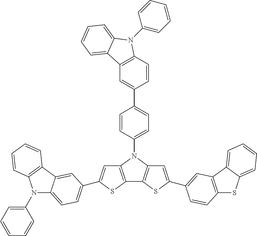
In the exemplary embodiment, the compound represented by Chemical Formula 1 may be selected from structures of the following Table 4.
TABLE 4
No. Chemical Formula
1
Figure US10522764-20191231-C00040
2
Figure US10522764-20191231-C00041
3
Figure US10522764-20191231-C00042
4
Figure US10522764-20191231-C00043
5
Figure US10522764-20191231-C00044
6
Figure US10522764-20191231-C00045
7
Figure US10522764-20191231-C00046
8
Figure US10522764-20191231-C00047
9
Figure US10522764-20191231-C00048
10
Figure US10522764-20191231-C00049
11
Figure US10522764-20191231-C00050
12
Figure US10522764-20191231-C00051
13
Figure US10522764-20191231-C00052
14
Figure US10522764-20191231-C00053
15
Figure US10522764-20191231-C00054
16
Figure US10522764-20191231-C00055
17
Figure US10522764-20191231-C00056
18
Figure US10522764-20191231-C00057
19
Figure US10522764-20191231-C00058
20
Figure US10522764-20191231-C00059
21
Figure US10522764-20191231-C00060
22
Figure US10522764-20191231-C00061
23
Figure US10522764-20191231-C00062
24
Figure US10522764-20191231-C00063
25
Figure US10522764-20191231-C00064
26
Figure US10522764-20191231-C00065
27
Figure US10522764-20191231-C00066
28
Figure US10522764-20191231-C00067
29
Figure US10522764-20191231-C00068
30
Figure US10522764-20191231-C00069
31
Figure US10522764-20191231-C00070
32
Figure US10522764-20191231-C00071
33
Figure US10522764-20191231-C00072
34
Figure US10522764-20191231-C00073
35
Figure US10522764-20191231-C00074
36
Figure US10522764-20191231-C00075
37
Figure US10522764-20191231-C00076
38
Figure US10522764-20191231-C00077
39
Figure US10522764-20191231-C00078
40
Figure US10522764-20191231-C00079
41
Figure US10522764-20191231-C00080
42
Figure US10522764-20191231-C00081
43
Figure US10522764-20191231-C00082
44
Figure US10522764-20191231-C00083
45
Figure US10522764-20191231-C00084
46
Figure US10522764-20191231-C00085
47
Figure US10522764-20191231-C00086
48
Figure US10522764-20191231-C00087
49
Figure US10522764-20191231-C00088
50
Figure US10522764-20191231-C00089
51
Figure US10522764-20191231-C00090
52
Figure US10522764-20191231-C00091
53
Figure US10522764-20191231-C00092
54
Figure US10522764-20191231-C00093
55
Figure US10522764-20191231-C00094
56
Figure US10522764-20191231-C00095
57
Figure US10522764-20191231-C00096
58
Figure US10522764-20191231-C00097
59
Figure US10522764-20191231-C00098
60
Figure US10522764-20191231-C00099
61
Figure US10522764-20191231-C00100
62
Figure US10522764-20191231-C00101
63
Figure US10522764-20191231-C00102
64
Figure US10522764-20191231-C00103
65
Figure US10522764-20191231-C00104
66
Figure US10522764-20191231-C00105
Hereinafter, a light-emitting element including the novel compound according to the present invention will be described with reference to the accompanying drawings. The structure of the light-emitting element including the compound is not limited by the accompanying drawings and the following description.
FIG. 1 is a cross-sectional view for illustrating the light-emitting element according to the exemplary embodiment of the present invention.
Referring to FIG. 1, a light-emitting element 100 includes a first electrode 20, a hole transportable layer 30, a light emitting layer 40, and a second electrode 50 formed on a base substrate 10. The light-emitting element 100 may be an organic light emitting diode (OLED).
The first electrode 20 may be formed of a conductive material on the base substrate 10. For example, the first electrode 20 may be a transparent electrode. In this case, the first electrode 20 may be formed of indium-tin oxide (ITO). Unlike this, the first electrode 20 may be an opaque (reflective) electrode. In this case, the first electrode 20 may have an ITO/silver (Ag)/ITO structure. The first electrode 20 may become an anode of the light-emitting element 100.
The hole transportable layer 30 is formed on the first electrode 20 to be interposed between the first electrode 20 and the light emitting layer 40. The hole transportable layer 30 includes a compound represented by the following Chemical Formula 1 as a hole transportable compound.
Figure US10522764-20191231-C00106
The compound represented by Chemical Formula 1 is the novel compound according to the present invention, and is substantially the same as that described in the above. Accordingly, a specific description of each of R1 to R4, La, and Ar1 will be omitted.
A wavelength of light emitted from the light emitting layer 40 may be changed according to a kind of the compound forming the light emitting layer 40.
The second electrode 50 may be formed of a conductive material on the light emitting layer 40. In the case where the first electrode 20 is a transparent electrode, the second electrode 50 may be an opaque (reflective) electrode. In this case, the second electrode 50 may be an aluminum electrode. Unlike this, in the case where the first electrode 20 is an opaque electrode, the second electrode 50 may be a transparent or translucent electrode. In this case, the second electrode 50 may have a thickness of 100 Å to 150 Å, and may be made of an alloy including magnesium and silver. The second electrode 50 may become a cathode of the light-emitting element 100.
Between the light emitting layer 40 and the second electrode 50, as an electron transportable layer, an electron transport layer and/or an electron injection layer may be formed.
In the case where a current flows between the first and second electrodes 20 and 50 of the light-emitting element 100, holes injected from the first electrode 20 to the light emitting layer 40 and electrons injected from the second electrode 50 to the light emitting layer 40 are combined to form excitons. In a process of transferring the exciton to a bottom state, light having a wavelength of a specific region band is generated. In this case, the exciton may be a singlet exciton or a triplet exciton. Accordingly, the light-emitting element 100 may provide light to the outside.
Although not illustrated in the drawings, the light-emitting element 100 may further include an electron transport layer (ETL) and an electron injection layer (EIL) disposed between the light emitting layer 40 and the second electrode 50. The electron transport layer and the electron injection layer may be sequentially laminated to be formed on the light emitting layer 40.
Further, the light-emitting element 100 may further include a first blocking layer (not illustrated) disposed between the first electrode 20 and the light emitting layer 40, and/or a second blocking layer (not illustrated) disposed between the light emitting layer 40 and the second electrode 50.
For example, the first blocking layer may be an electron blocking layer (EBL) disposed between the hole transportable layer 30 and the light emitting layer 40 to prevent the electrons injected from the second electrode 50 from flowing through the light emitting layer 40 into the hole transportable layer 30. Further, the first blocking layer may be an exciton blocking layer preventing the exciton formed in the light emitting layer 40 from being diffused in a direction of the first electrode 20 to become extinct without light emission.
In this case, the first blocking layer may include the aforementioned compound according to the present invention.
The second blocking layer may be a hole blocking layer (HBL) disposed between the light emitting layer 40 and the second electrode 50 and specifically between the light emitting layer 40 and the electron transport layer to prevent the holes from flowing from the first electrode 20 through the light emitting layer 40 into the electron transport layer. Further, the second blocking layer may be an exciton blocking layer preventing the exciton formed in the light emitting layer 40 from being diffused in a direction of the second electrode 50 to become extinct without light emission.
If a thickness of each of the first and second blocking layers is adjusted to match a resonance length of the light-emitting element 100, light emitting efficiency may be increased, and the thickness may be adjusted so that the exciton is formed at the center of the light emitting layer 40.
Referring to FIG. 2, a light-emitting element 102 includes a first electrode 20, a hole transportable layer 32, a light emitting layer 40, and a second electrode 50 formed on a base substrate 10. Since the light-emitting element is substantially the same as that illustrated in FIG. 1 with the exception of the hole transportable layer 32, an overlapping description will be omitted.
The hole transportable layer 32 includes the compound represented by Chemical Formula 1, and a P-type dopant. Since the compound included in the hole transportable layer 32 is substantially the same as that described in the above, an overlapping specific description will be omitted.
The P-type dopant may include a P-type organic dopant, and/or a P-type inorganic dopant.
Specific examples of the P-type organic dopant may include compounds represented by the following Chemical Formulas 7 to 11, hexadecafluorophthalocyanine (F16CuPc), 11,11,12,12-tetracyanonaphtho-2,6-quinodimethane (TNAP), 3,6-difluoro-2,5,7,7,8,8-hexacyano-quinodimethane (F2-HCNQ), tetracyanoquinodimethane (TCNQ), or the like. The examples may be used alone or in combination of two or more thereof.
Figure US10522764-20191231-C00107
In Chemical Formula 7, R may represent a cyano group, a sulfone group, a sulfoxide group, a sulfonamide group, a sulfonate group, a nitro group, or a trifluoromethyl group.
Figure US10522764-20191231-C00108
In Chemical Formula 11, m and n may each independently represent an integer of 1 to 5, and Y1 and Y2 may each independently represent an aryl group having 6 to 20 carbon atoms or a heteroaryl group having 2 to 20 carbon atoms. In this case, hydrogen of the aryl group or the heteroaryl group represented by Y1 and Y2 may be unsubstituted or substituted by an alkyl group having 1 to 5 carbon atoms, an alkoxy group having 1 to 5 carbon atoms, or a hydroxyl group, and hydrogens of substituted or unsubstituted Y1 and Y2 may be each independently unsubstituted or substituted by a halogen group.
For example, the compound represented by Chemical Formula 11 may include a compound represented by the following Chemical Formula 11a or the following Chemical Formula 11b.
Figure US10522764-20191231-C00109
Examples of the P-type inorganic dopant may include metal oxides, metal halides, or the like. Specific examples of the P-type inorganic dopant may include MoO3, V2O5, WO3, SnO2, ZnO, MnO2, CoO2, ReO3, TiO2, FeCl3, SbCl5, MgF2, or the like. The examples may be used alone or in combination of two or more thereof.
A content of the P-type dopant may be about 0.5 parts by weight to about 20 parts by weight based on 100 parts by weight of the novel compound according to the present invention, which is a hole transportable compound. For example, the content of the P-type dopant may be about 0.5 parts by weight to about 15 parts by weight or about 0.5 parts by weight to about 5 parts by weight based on 100 parts by weight of the hole transportable compound. Unlike this, the content of the P-type dopant may be about 1 part by weight to 10 parts by weight, 1 part by weight to 5 parts by weight, 1.5 parts by weight to 6 parts by weight, or 2 parts by weight to 5 parts by weight based on 100 parts by weight of the hole transportable compound.
In the case where the content of the P-type dopant is about 0.5 parts by weight to about 20 parts by weight based on 100 parts by weight of the hole transportable compound, the P-type dopant may not degrade physical properties of the hole transportable compound and may prevent generation of an excessive leakage current. Further, energy barriers at interfaces with upper and lower layers coming into contact with the hole transportable layer 32 may be reduced by the P-type dopant.
Although not illustrated in the drawings, the light-emitting element 102 may further include the electron transport layer, the electron injection layer, the first blocking layer, and/or the second blocking layer. Since the layers is substantially the same as those described in the light-emitting element 100 of FIG. 1, a specific description will be omitted. In the case where the light-emitting element 102 includes the first blocking layer, the first blocking layer may include the aforementioned compound according to the present invention.
Meanwhile, the light-emitting element 100 illustrated in FIG. 1 may further include an interlayer (not illustrated). The interlayer may be disposed between the first electrode 20 and the hole transportable layer 30 of FIG. 1, and may be formed of the compound used as the P-type dopant described in FIG. 2.
Referring to FIG. 3, a light-emitting element 104 includes a first electrode 20, a hole transportable layer 34, a light emitting layer 40, and a second electrode 50 formed on a base substrate 10. Since the light-emitting element is substantially the same as that illustrated in FIG. 1 with the exception of the hole transportable layer 34, an overlapping description will be omitted.
The hole transportable layer 34 includes a first layer 33 a coming into contact with the first electrode 20, and a second layer 33 b disposed between the first layer 33 a and the light emitting layer 40. That is, the hole transportable layer 34 may have a two-layered structure. Further, the hole transportable layer 34 may have a multilayered structure of two layers or more including the first and second layers 33 a and 33 b.
The first and second layers 33 a and 33 b may include the same kind of hole transportable compound. By having components of the hole transportable compounds included in the first layer 33 a and the second layer 33 b to be the same as each other, physical and chemical defects that may occur at an interface between heteromaterials may be reduced, and thus holes may be easily injected into the light emitting layer. In another aspect, if the same host material is used in the first layer 33 a and the second layer 33 b, since the first layer 33 a and the second layer 33 b may be continuously formed in one chamber, a manufacturing process is simplified and a manufacturing time may be shortened. Moreover, since physical properties such as a glass transition temperature between the adjacent layers become similar to each other, durability of the element may be increased.
The first layer 33 a includes the novel compound according to the present invention represented by Chemical Formula 1 as the hole transportable compound, and the P-type dopant. The first layer 33 a is substantially the same as the hole transportable layer 32 described in FIG. 2 with the exception of the thickness. Accordingly, an overlapping description will be omitted.
The second layer 33 b includes the novel compound according to the present invention represented by Chemical Formula 1 as the hole transportable compound, and the hole transportable compound constituting the second layer 33 b may be the same as the hole transportable compound constituting the first layer 33 a. Since the second layer 33 b is substantially the same as the hole transportable layer 30 described in FIG. 1 with the exception of the thickness, an overlapping detailed description will be omitted.
Unlike this, the first and second layers 33 a and 33 b may include different kinds of hole transportable compounds. The hole transportable compounds constituting the first and second layers 33 a and 33 b are the novel compounds according to the present invention represented by Chemical Formula 1, and R1 to R4, La, and Ar1 may be each independently different from each other. In this case, the compound constituting each of the first and second layers 33 a and 33 b may be selected to have a HOMO value for effectively transferring holes to the light emitting layer 40.
Additionally, the second layer 33 b may further include the P-type dopant together with the hole transportable compound. In this case, the kinds of the P-type dopants doped on the first layer 33 a and the second layer 33 b may be different from each other, and even though the same kind is used, doping amounts may be different from each other. For example, the content P1 of the P-type dopant doped on the first layer 33 a and the content P2 of the P-type dopant doped on the second layer 33 b may satisfy a relationship of the following Equation 1.
P1/P2≥1  [Equation 1]
In Equation 1,
“P1” is the content of the doped P-type dopant based on 100 parts by weight of the hole transportable compound in the first layer 33 a, and “P2” is the content of the doped P-type dopant based on 100 parts by weight of the hole transportable compound in the second layer 33 b.
For example, the content of the P-type dopant doped on the first layer 33 a may be in the range of 0.3 to 20 parts by weight, 1 to 15 parts by weight, 2 to 10 parts by weight, or 4 to 6 parts by weight based on 100 parts by weight of the hole transportable compound. Further, the content of the P-type dopant doped on the second layer 33 b may be in the range of 0.3 to 20 parts by weight, 0.5 to 10 parts by weight, 1 to 8 parts by weight, or 2 to 4 parts by weight based on 100 parts by weight of the hole transportable compound.
Further, although not illustrated in the drawings, the light-emitting element 104 may further include the electron transport layer, the electron injection layer, the first blocking layer, and/or the second blocking layer. Since the layers is substantially the same as those described in the light-emitting element 100 of FIG. 1, a specific description will be omitted.
Each of the aforementioned light-emitting elements 100, 102, and 104 may include the novel compound according to the present invention represented by Chemical Formula 1, and thus the light-emitting elements 100, 102, and 104 may have excellent thermal stability, and simultaneously light emitting efficiency may be improved and a life-span may be lengthened.
FIGS. 1 to 3 illustrate that the light-emitting elements 100, 102, and 104 are directly formed on the base substrate 10, but a thin film transistor as a switching element driving a pixel may be disposed between the first electrode 20 and the base substrate 10 of each of the light-emitting elements 100, 102, and 104. In this case, the first electrode 20 may become a pixel electrode connected to the thin film transistor. In the case where the first electrode 20 is the pixel electrode, the first electrodes 20 may be disposed to be separated from each other in a plurality of pixels and a partition wall pattern formed along an edge of the first electrode 20 may be formed on the base substrate 10 to isolate layers laminated on the first electrodes 20 disposed in the pixels that are adjacent to each other from each other. That is, although not illustrated in the drawings, the light-emitting elements 100, 102, and 104 may be used in a display device displaying an image without a backlight.
Further, the light-emitting elements 100, 102, and 104 may be used as a lighting device.
As described above, the light-emitting elements 100, 102, and 104 exemplified in the present invention may be used in various electronic devices such as the display device or the lighting device.
EXAMPLES
Hereinafter, the novel compounds according to the present invention will be described in more detail through specific Examples according to the present invention. The Examples exemplified below are set forth only for the detailed description of the invention, but are not to be construed to limit the scope of the right.
Example 1
Figure US10522764-20191231-C00110
After nitrogen was charged in the 1 L three-neck round bottom flask, compound A (37.9 mmol, 20 g), compound B (41.7 mmol, 15.4 g), 200 mL of tetrahydrofuran (THF), and 100 mL of ethanol (EtOH) were added and agitated for 30 minutes. Further, potassium carbonate (K2CO3) (151.9 mmol, 21.0 g) was dissolved in 100 mL of water (H2O), and then the solution is added to the 1 L three-neck round bottom flask. Subsequently, after tetrakis(triphenylphosphine)palladium (Pd(PPh3)4, 1.5 mmol, 1.76 g) was added to the 1 L three-neck round bottom flask, light was blocked and reflux was performed for 6 hours.
The reaction mixture was cooled, extracted and concentrated by using ethyl acetate (EA) and distilled water, dissolved in 100 mL of tetrahydrofuran (THF), and added to 1 L of methanol, followed by agitation for 20 minutes and filtration to obtain 21.1 g of compound 1 that was the light grey solid (yield 80%).
MALDI-TOF: m/z=688.1923 (C47H32N2S2=688.2)
Example 2
Figure US10522764-20191231-C00111
After nitrogen was charged in the 1 L three-neck round bottom flask, compound C (38.7 mmol, 20 g), compound B (42.5 mmol, 15.7 g), 200 mL of tetrahydrofuran (THF), and 100 mL of ethanol (EtOH) were added and agitated for 30 minutes. Further, potassium carbonate (K2CO3) (154.8 mmol, 21.4 g) was dissolved in 100 mL of water (H2O), and then the solution is added to the 1 L three-neck round bottom flask. Subsequently, after tetrakis(triphenylphosphine)palladium (Pd(PPh3)4, 1.5 mmol, 1.79 g) was added to the 1 L three-neck round bottom flask, light was blocked and reflux was performed for 5 hours.
The reaction mixture was cooled, extracted and concentrated by using ethyl acetate (EA) and distilled water, dissolved in 100 mL of tetrahydrofuran (THF), and added to 1 L of methanol, followed by agitation for 20 minutes and filtration to obtain 23.5 g of compound 2 that was the light grey solid (yield 90%).
MALDI-TOF: m/z=678.2320 (C44H36N2S3=678.1)
Example 3
Figure US10522764-20191231-C00112
After nitrogen was charged in the 1 L three-neck round bottom flask, compound D (30.6 mmol, 20 g), compound B (33.7 mmol, 12.4 g), 200 mL of tetrahydrofuran (THF), and 100 mL of ethanol (EtOH) were added and agitated for 30 minutes. Further, potassium carbonate (K2CO3) (122.7 mmol, 16.9 g) was dissolved in 100 mL of water (H2O), and then the solution is added to the 1 L three-neck round bottom flask. Subsequently, after tetrakis(triphenylphosphine)palladium (Pd(PPh3)4, 1.2 mmol, 1.42 g) was added to the 1 L three-neck round bottom flask, light was blocked and reflux was performed for 6 hours.
The reaction mixture was cooled, extracted and concentrated by using ethyl acetate (EA) and distilled water, dissolved in 100 mL of tetrahydrofuran (THF), and added to 1 L of methanol, followed by agitation for 20 minutes and filtration to obtain 19.8 g of compound 3 that was the light grey solid (yield 80%).
MALDI-TOF: m/z=813.1983 (C56H35N3S2=813.2)
Example 4
Figure US10522764-20191231-C00113
After nitrogen was charged in the 1 L three-neck round bottom flask, compound E (48.4 mmol, 20 g), compound B (106.4 mmol, 39.3 g), 200 mL of tetrahydrofuran (THF), and 100 mL of ethanol (EtOH) were added and agitated for 30 minutes. Further, potassium carbonate (K2CO3) (387.2 mmol, 53.52 g) was dissolved in 150 mL of water (H2O), and then the solution is added to the 1 L three-neck round bottom flask. Subsequently, after tetrakis(triphenylphosphine)palladium (Pd(PPh3)4, 3.87 mmol, 4.47 g) was added to the 1 L three-neck round bottom flask, light was blocked and reflux was performed for 12 hours.
The reaction mixture was cooled, extracted and concentrated by using ethyl acetate (EA) and distilled water, dissolved in 100 mL of tetrahydrofuran (THF), and added to 1 L of methanol, followed by agitation for 20 minutes and filtration to obtain 25.1 g of compound 4 that was the light grey solid (yield 71%).
MALDI-TOF: m/z=737.2032 (C50H31N3S2=737.2)
Example 5
Figure US10522764-20191231-C00114
After nitrogen was charged in the 1 L three-neck round bottom flask, compound F (59.8 mmol, 20 g), compound G (65.8 mmol, 25.0 g), 200 mL of tetrahydrofuran (THF), and 100 mL of ethanol (EtOH) were added and agitated for 30 minutes. Further, potassium carbonate (K2CO3) (239.3 mmol, 33.07 g) was dissolved in 100 mL of water (H2O), and then the solution is added to the 1 L three-neck round bottom flask. Subsequently, after tetrakis(triphenylphosphine)palladium (Pd(PPh3)4, 2.3 mmol, 2.77 g) was added to the 1 L three-neck round bottom flask, light was blocked and reflux was performed for 12 hours.
The reaction mixture was cooled, extracted and concentrated by using ethyl acetate (EA) and distilled water, dissolved in 100 mL of tetrahydrofuran (THF), and added to 1 L of methanol, followed by agitation for 20 minutes and filtration to obtain 26.5 g of compound 5 that was the light grey solid (yield 87%).
MALDI-TOF: m/z=508.1235 (C28H16N2S4=508.0)
Example 6
Figure US10522764-20191231-C00115
After nitrogen was charged in the 1 L three-neck round bottom flask, compound E (48.4 mmol, 20 g), compound G (106.4 mmol, 40.6 g), 200 mL of tetrahydrofuran (THF), and 100 mL of ethanol (EtOH) were added and agitated for 30 minutes. Further, potassium carbonate (K2CO3) (387.2 mmol, 53.52 g) was dissolved in 150 mL of water (H2O), and then the solution is added to the 1 L three-neck round bottom flask. Subsequently, after tetrakis(triphenylphosphine)palladium (Pd(PPh3)4, 3.87 mmol, 4.47 g) was added to the 1 L three-neck round bottom flask, light was blocked and reflux was performed for 12 hours.
The reaction mixture was cooled, extracted and concentrated by using ethyl acetate (EA) and distilled water, dissolved in 100 mL of tetrahydrofuran (THF), and added to 1 L of methanol, followed by agitation for 20 minutes and filtration to obtain 20.5 g of compound 6 that was the light grey solid (yield 55%).
MALDI-TOF: m/z=760.9824 (C42H23N3S6=761.0)
Example 7
Figure US10522764-20191231-C00116
After nitrogen was charged in the 1 L three-neck round bottom flask, compound H (35.4 mmol, 20 g), compound G (39.04 mmol, 14.89 g), 200 mL of tetrahydrofuran (THF), and 100 mL of ethanol (EtOH) were added and agitated for 30 minutes. Further, potassium carbonate (K2CO3) (141.9 mmol, 19.62 g) was dissolved in 100 mL of water (H2O), and then the solution is added to the 1 L three-neck round bottom flask. Subsequently, after tetrakis(triphenylphosphine)palladium (Pd(PPh3)4, 1.42 mmol, 1.64 g) was added to the 1 L three-neck round bottom flask, light was blocked and reflux was performed for 12 hours.
The reaction mixture was cooled, extracted and concentrated by using ethyl acetate (EA) and distilled water, dissolved in 100 mL of tetrahydrofuran (THF), and added to 1 L of methanol, followed by agitation for 20 minutes and filtration to obtain 18.3 g of compound 7 that was the light grey solid (yield 70%).
MALDI-TOF: m/z=737.2100 (C50H31N3S2=737.2)
Example 8
Figure US10522764-20191231-C00117
After nitrogen was charged in the 1 L three-neck round bottom flask, compound I (30.0 mmol, 20 g), compound B (66.0 mmol, 24.38 g), 200 mL of tetrahydrofuran (THF), and 100 mL of ethanol (EtOH) were added and agitated for 30 minutes. Further, potassium carbonate (K2CO3) (240.0 mmol, 33.18 g) was dissolved in 150 mL of water (H2O), and then the solution is added to the 1 L three-neck round bottom flask. Subsequently, after tetrakis(triphenylphosphine)palladium (Pd(PPh3)4, 2.4 mmol, 2.77 g) was added to the 1 L three-neck round bottom flask, light was blocked and reflux was performed for 12 hours.
The reaction mixture was cooled, extracted and concentrated by using ethyl acetate (EA) and distilled water, dissolved in 100 mL of tetrahydrofuran (THF), and added to 1 L of methanol, followed by agitation for 20 minutes and filtration to obtain 23.6 g of compound 8 that was the light grey solid (yield 79%).
MALDI-TOF: m/z=990.2561 (C64H38N4S4=990.2)
Example 9
Figure US10522764-20191231-C00118
After nitrogen was charged in the 1 L three-neck round bottom flask, compound F (59.8 mmol, 20 g), compound B (65.8 mmol, 24.3 g), 200 mL of tetrahydrofuran (THF), and 100 mL of ethanol (EtOH) were added and agitated for 30 minutes. Further, potassium carbonate (K2CO3) (239.3 mmol, 33.07 g) was dissolved in 100 mL of water (H2O), and then the solution is added to the 1 L three-neck round bottom flask. Subsequently, after tetrakis(triphenylphosphine)palladium (Pd(PPh3)4, 2.3 mmol, 2.77 g) was added to the 1 L three-neck round bottom flask, light was blocked and reflux was performed for 12 hours.
The reaction mixture was cooled, extracted and concentrated by using ethyl acetate (EA) and distilled water, dissolved in 100 mL of tetrahydrofuran (THF), and added to 1 L of methanol, followed by agitation for 20 minutes and filtration to obtain 23.5 g of compound 9 that was the light grey solid (yield 79%).
MALDI-TOF: m/z=496.9564 (C32H20N2S2=496.1)
Example 10
Figure US10522764-20191231-C00119
After nitrogen was charged in the 1 L three-neck round bottom flask, compound F (59.8 mmol, 20 g), compound J (65.8 mmol, 30.3 g), 200 mL of tetrahydrofuran (THF), and 100 mL of ethanol (EtOH) were added and agitated for 30 minutes. Further, potassium carbonate (K2CO3) (239.3 mmol, 33.07 g) was dissolved in 100 mL of water (H2O), and then the solution is added to the 1 L three-neck round bottom flask. Subsequently, after tetrakis(triphenylphosphine)palladium (Pd(PPh3)4, 2.3 mmol, 2.77 g) was added to the 1 L three-neck round bottom flask, light was blocked and reflux was performed for 12 hours.
The reaction mixture was cooled, extracted and concentrated by using ethyl acetate (EA) and distilled water, dissolved in 100 mL of tetrahydrofuran (THF), and added to 1 L of methanol, followed by agitation for 20 minutes and filtration to obtain 29.8 g of compound 10 that was the light grey solid (yield 85%).
MALDI-TOF: m/z=587.1147 (C38H25NS2Si=587.1)
Example 11
Figure US10522764-20191231-C00120
After nitrogen was charged in the 1 L three-neck round bottom flask, compound K (33.7 mmol, 20 g), compound B (67.4 mmol, 24.9 g), 200 mL of tetrahydrofuran (THF), and 100 mL of ethanol (EtOH) were added and agitated for 30 minutes. Further, potassium carbonate (K2CO3) (74.1 mmol, 10.25 g) was dissolved in 100 mL of water (H2O), and then added to the 1 L three-neck round bottom flask. Subsequently, after tetrakis(triphenylphosphine)palladium (Pd(PPh3)4, 2.1 mmol, 2.53 g) was added to the 1 L three-neck round bottom flask, reflux was performed for 12 hours.
The reaction mixture was cooled, extracted and concentrated by using ethyl acetate (EA) and distilled water, and added to 1 L of methanol, followed by agitation for 20 minutes and filtration to obtain 30.5 g of compound 11 that was the light grey solid (yield 91%).
MALDI-TOF: m/z=978.2851 (C68H42N4S2=978.3)
Example 12
Figure US10522764-20191231-C00121
After nitrogen was charged in the 1 L three-neck round bottom flask, compound K (56.8 mmol, 37 g), compound M (113.5 mmol, 25.9 g), 200 mL of tetrahydrofuran (THF), and 100 mL of ethanol (EtOH) were added and agitated for 30 minutes. Further, potassium carbonate (K2CO3) (112.5 mmol, 17.27 g) was dissolved in 100 mL of water (H2O), and then the solution is added to the 1 L three-neck round bottom flask. Subsequently, after tetrakis(triphenylphosphine)palladium (Pd(PPh3)4, 2.3 mmol, 2.54 g) was added to the 1 L three-neck round bottom flask, reflux was performed for 12 hours.
The reaction mixture was cooled, extracted and concentrated by using ethyl acetate (EA) and distilled water, and added to 2 L of methanol, followed by agitation for 20 minutes and filtration to obtain 41.2 g of compound 12 that was the light grey solid (yield 84%).
MALDI-TOF: m/z=860.1448 (C56H32N2S4=860.1)
Comparative Examples 1 to 4
The compounds having the structures of the following Chemical Formulas a, b, c, and d were commercially obtained or manufactured to be used as Comparative Examples 1 to 4.
Figure US10522764-20191231-C00122

Manufacturing of Light-Emitting Elements A-1 to A-10
On the first electrode formed of indium-tin oxide (ITO), the compound according to Example 1 as the host material was evaporated at the rate of 1 Å/sec, and simultaneously, the P-type dopant (HAT-CN) represented by the following Chemical Formula 12 was co-evaporated at the ratio of about 5 parts by weight based on 100 parts by weight of the host material to form the first layer having the thickness of 100 Å. On the first layer, the compound according to Example 1 was evaporated in the thickness of 300 Å to form the second layer.
On the second layer, mCBP represented by the following Chemical Formula 13 and Ir(ppy)3 represented by Chemical Formula 14 were co-evaporated at the weight ratio of 100:9 to form the light emitting layer having the thickness of about 300 Å, and on the light emitting layer, mCBP was evaporated again in the thickness of about 50 Å to form the blocking layer.
On the blocking layer, BPhen represented by the following Chemical Formula 15 and Alga represented by the following Chemical Formula 16 were co-evaporated at the weight ratio of 50:50 to form the electron transport layer having the thickness of about 400 Å. Subsequently, on the electron transport layer, the electron injection layer having the thickness of about 10 Å was formed by using Liq represented by the following Chemical Formula 17.
On the electron injection layer, the second electrode using the aluminum thin film having the thickness of 1,000 Å was formed.
Figure US10522764-20191231-C00123
Figure US10522764-20191231-C00124
Light-emitting element A-1 including the compound according to Example 1 of the present invention was manufactured by the aforementioned method.
Further, light-emitting elements A-2 to A-10 were manufactured through the process that was substantially the same as the process of manufacturing the light-emitting element A-1, except that the hole transportable layer was formed by using each of the compounds according to Examples 2 to 10 as the host material.
Manufacturing of Comparative Elements 1 to 4
Comparative elements 1 to 4 were manufactured through the process that was substantially the same as the process of manufacturing the light-emitting element A-1, except that the first layer and the second layer were formed by using the compounds according to Comparative Examples 1 to 4 as the host material.
Evaluation of Power Efficiency and Life-Span of Light-Emitting Element-1
With respect to each of the light-emitting elements A-1 to A-10 and the comparative elements 1 to 4, after the silant for UV curing was dispensed at the edge of the cover glass to which the getter was attached in the globe box under the nitrogen atmosphere, each of the light-emitting elements and the comparative elements was adhered to the cover glass, and UV light was radiated to perform curing. With respect to each of light-emitting elements A-1 to A-10 and comparative elements 1 to 4 as prepared in the above, power efficiency was measured based on the value when luminance was 500 cd/m2. The result is described in Table 5.
Further, the life-span of each of light-emitting elements A-1 to A-10 and comparative elements 1 to 4 was measured by using the life-span measurement apparatus installed in the oven for measurement constantly maintaining the temperature of about 85° C. The result is described in Table 5.
In Table 5, a unit of the measurement result of power efficiency is lm/W. Further, in Table 5, in the case where initial luminance of the light-emitting element is 1,000 cd/m2, T75 means a time required until luminance of the light-emitting element becomes 75% of the initial luminance.
TABLE 5
Power efficiency Life-span
Element No. [lm/W] (T75@85° C. [hr])
Light-emitting element A-1 29.0 673
Light-emitting element A-2 20.5 479
Light-emitting element A-3 28.0 647
Light-emitting element A-4 26.2 606
Light-emitting element A-5 20.4 467
Light-emitting element A-6 16.3 379
Light-emitting element A-7 22.8 533
Light-emitting element A-8 24.2 558
Light-emitting element A-9 20.8 476
Light-emitting element A-10 18.6 424
Comparative element 1 9.2 227
Comparative element 2 10.5 268
Comparative element 3 11.0 279
Comparative element 4 10.3 235
Referring to Table 5, it can be seen that power efficiency of each of the light-emitting elements manufactured by using the compounds according to Examples 1 to 10 of the present invention is at least 16.3 lm/W and is better than power efficiency of comparative elements 1 to 4 which is 9.2 lm/W to 11.0 lm/W.
Further, it can be seen that the life-spans of the light-emitting elements manufactured by using the compounds according to Examples 1 to 10 of the present invention are at least about 379 hours and mostly about 300 hours or more. On the other hand, it can be seen that as compared to the life-span of comparative elements 1 to 4 of about 279 hours or less, the life-spans of the light-emitting elements including the compounds according to Examples 1 to 10 of the present invention are better than those of comparative elements 1 to 4.
Further, in consideration of evaluation of the life-span property of the light-emitting element performed under the acceleration condition (severe condition) of 85° C., from the fact that that the life-span property of the light-emitting elements including the compounds according to Examples 1 to 10 of the present invention is better than that of comparative elements 1 to 4, it can be seen that heat resistance of the light-emitting elements manufactured by using the compound according to the present invention is better than that of comparative elements 1 to 4.
Manufacturing of Light-Emitting Elements B-1 to B-4
On the first electrode formed of indium-tin oxide (ITO), HAT-CN represented by Chemical Formula 12 was evaporated in the thickness of about 100 Å to form the first layer, and on the first layer, NPB (N,N′-diphenyl-N,N′-bis(1-naphthyl)-1,1′-biphenyl-4,4′-diamine) was evaporated in the thickness of about 300 Å to form the second layer.
On the second layer, the first blocking layer having the thickness of about 100 Å was formed of the compound according to Example 1, on the first blocking layer, mCBP represented by Chemical Formula 13 and Ir(ppy)3 represented by Chemical Formula 14 were co-evaporated at the weight ratio of 100:9 to form the light emitting layer having the thickness of about 300 Å, and on the light emitting layer, mCBP was evaporated again in the thickness of about 50 Å to form the second blocking layer.
Then, on the second blocking layer, BPhen represented by Chemical Formula 15 and Alga represented by Chemical Formula 16 were co-evaporated at the weight ratio of 50:50 to form the electron transport layer having the thickness of about 400 Å. Subsequently, on the electron transport layer, the electron injection layer having the thickness of about 10 Å was formed by using Liq represented by Chemical Formula 17.
On the electron injection layer, the second electrode using the aluminum thin film having the thickness of 1,000 Å was formed to manufacture light-emitting element B-1 including the compound according to Example 1 of the present invention.
Light-emitting elements B-2, B-3, and B-4 were manufactured through the process that was substantially the same as the process of manufacturing the light-emitting element B-1, except that the first blocking layer was manufactured by using each of the compounds according to Examples 3, 5, and 8 of the present invention.
Manufacturing of Comparative Elements 5 and 6
Comparative element 5 was manufactured through the process that was substantially the same as the process of manufacturing the light-emitting element B-1, except that the first blocking layer was manufactured by using the compound according to Comparative Example 1 represented by Chemical Formula a.
Further, comparative element 6 was manufactured through the process that was substantially the same as the process of manufacturing the light-emitting element B-1, except that the first blocking layer was manufactured by using the compound according to Comparative Example 4 represented by Chemical Formula d.
Evaluation of Power Efficiency and Life-Span of Light-Emitting Element-2
With respect to each of light-emitting elements B-1 to B-4 and comparative elements 5 and 6 as prepared in the above, power efficiency was measured based on the value when luminance was 500 cd/m2 by the method that was substantially the same as the power efficiency measurement experiment of the light-emitting elements A-1 to A-10.
Further, the life-span of each of light-emitting elements B-1 to B-4 and comparative elements 5 and 6 was measured by the method that was substantially the same as in the aforementioned life-span evaluation experiment of light-emitting elements A-1 to A-10.
The results of power efficiency and the life-span of each of the light-emitting elements B-1 to B-4 and comparative elements 5 and 6 are described in Table 6. In Table 6, a unit of the measurement result of power efficiency is lm/W. Further, in Table 6, in the case where initial luminance of the light-emitting element is 1,000 cd/m2, T75 means a time required until luminance of the light-emitting element becomes 75% of the initial luminance.
TABLE 6
Power efficiency Life-span
Element No. [lm/W] (T75@85° C. [hr])
Light-emitting element B-1 23.8 554
Light-emitting element B-2 22.9 537
Light-emitting element B-3 16.8 387
Light-emitting element B-4 19.9 459
Comparative element 5 7.9 185
Comparative element 6 8.4 196
Referring to Table 6, it can be seen that power efficiency of each of light-emitting elements B-1 to B-4 manufactured by using the compounds according to the present invention is at least 16.8 lm/W but power efficiency of comparative element 5 is just about 7.9 lm/W and power efficiency of comparative element 6 is just about 8.4 lm/W.
Further, it can be seen that the life-span of each of light-emitting elements B-1 to B-4 is at least about 387 hours, and as compared to the life-spans of comparative elements 5 and 6 which are about 185 hours and about 196 hours, respectively, the life-spans of light-emitting elements B-1 to B-4 are relatively longer than that of comparative elements 5 and 6.
Further, in consideration of evaluation of the life-span property of the light-emitting element performed under the acceleration condition (severe condition) of 85° C., from the fact that that the life-span property of the light-emitting element including the compound according to the present invention is better than that of comparative elements 5 and 6, it can be seen that heat resistance of the light-emitting element manufactured by using the compound according to the present invention is good.
Manufacturing of Light-Emitting Elements C-1 to C-4
On the first electrode formed of indium-tin oxide (ITO), NPB as the host material was evaporated at the rate of 1 Å/sec, and simultaneously, the P-type dopant (HAT-CN) represented by the following Chemical Formula 12 was co-evaporated at the ratio of about 5 parts by weight based on 100 parts by weight of the host material to form the first layer having the thickness of 100 Å. On the first layer, NPB was evaporated in the thickness of 300 Å to form the second layer. On the second layer, the first blocking layer having the thickness of about 100 Å was formed of the compound according to Example 3, on the first blocking layer, mCBP represented by Chemical Formula 13 and Ir(ppy)3 represented by Chemical Formula 14 were co-evaporated at the weight ratio of 100:9 to form the light emitting layer having the thickness of about 300 Å, and on the light emitting layer, mCBP was evaporated again in the thickness of about 50 Å to form the second blocking layer.
Then, on the second blocking layer, BPhen represented by Chemical Formula 15 and Alga represented by Chemical Formula 16 were co-evaporated at the weight ratio of 50:50 to form the electron transport layer having the thickness of about 400 Å. Subsequently, on the electron transport layer, the electron injection layer having the thickness of about 10 Å was formed by using Liq represented by Chemical Formula 17.
On the electron injection layer, the second electrode using the aluminum thin film having the thickness of 1,000 Å was formed to manufacture light-emitting element C-1 including the compound according to Example 3 of the present invention.
Light-emitting elements C-2, C-3, and C-4 were manufactured through the process that was substantially the same as the process of manufacturing the light-emitting element C-1, except that the first blocking layer was manufactured by using each of the compounds according to Examples 5, 8, and 10 of the present invention.
Manufacturing of Comparative Elements 7 and 8
Comparative element 7 was manufactured through the process that was substantially the same as the process of manufacturing the light-emitting element C-1, except that the first blocking layer was manufactured by using the compound according to Comparative Example 1 represented by Chemical Formula a.
Comparative element 8 was manufactured through the process that was substantially the same as the process of manufacturing the light-emitting element C-1, except that the first blocking layer was manufactured by using the compound according to Comparative Example 4 represented by Chemical Formula d.
Evaluation of Power Efficiency and Life-Span of Light-Emitting Element-3
With respect to each of light-emitting elements C-1 to C-4 and comparative elements 7 and 8 as prepared in the above, power efficiency was measured based on the value when luminance is 500 cd/m2 by the method that was substantially the same as in the power efficiency measurement experiment of the light-emitting elements A-1 to A-10.
Further, the life-span of each of light-emitting elements C-1 to C-4 and comparative elements 7 and 8 was measured by the method that was substantially the same as the aforementioned life-span evaluation experiment of light-emitting elements A-1 to A-10.
The results of power efficiency and the life-span of each of the light-emitting elements C-1 to C-4 and comparative elements 7 and 8 are described in Table 7. In Table 7, a unit of the measurement result of power efficiency is lm/W. Further, in Table 7, in the case where initial luminance of the light-emitting element is 1,000 cd/m2, T75 means a time required until luminance of the light-emitting element becomes 75% of the initial luminance.
TABLE 7
Power efficiency Life-span
Element No. [lm/W] (T75@85° C. [hr])
Light-emitting element C-1 21.0 483
Light-emitting element C-2 15.3 354
Light-emitting element C-3 18.2 419
Light-emitting element C-4 14.0 318
Comparative element 7 8.2 201
Comparative element 8 7.7 179
Referring to Table 7, it can be seen that power efficiency of each of light-emitting elements C-1 to C-4 is at least 14.0 lm/W and thus power efficiency of about 10 lm/W or more is exhibited, but power efficiency of comparative element 7 is just about 8.2 lm/W and power efficiency of comparative element 8 is about 7.7 lm/W.
Further, it can be seen that the life-span of each of light-emitting elements C-1 to C-4 is at least about 318 hours, and as compared to the life-spans of comparative element 7 and comparative element 8 which are about 201 hours and about 179 hours, the life-span of light-emitting elements according to the present invention is long.
Further, in consideration of evaluation of the life-span property of the light-emitting element performed under the acceleration condition (severe condition) of 85° C., from the fact that the life-span property of the light-emitting element including the compound according to the present invention is better than that of comparative elements 7 and 8, it can be seen that heat resistance of the light-emitting element manufactured by using the compound according to the present invention is good.
Manufacturing of Light-Emitting Elements D-1 to D-4
On the first electrode formed of indium-tin oxide (ITO), the compound according to Example 2 as the host material was evaporated at the rate of 1 Å/sec, and simultaneously, the P-type dopant (HAT-CN) represented by the following Chemical Formula 12 was co-evaporated at the ratio of about 5 parts by weight based on 100 parts by weight of the host material to form the first layer having the thickness of 100 Å. On the first layer, NPB was evaporated in the thickness of 300 Å to form the second layer. On the second layer, mCBP represented by Chemical Formula 13 and Ir(ppy)3 represented by Chemical Formula 14 were co-evaporated at the weight ratio of 100:9 to form the light emitting layer having the thickness of about 300 Å, and on the light emitting layer, mCBP was evaporated again in the thickness of about 50 Å to form the blocking layer.
Then, on the blocking layer, BPhen represented by Chemical Formula 15 and Alga represented by Chemical Formula 16 were co-evaporated at the weight ratio of 50:50 to form the electron transport layer having the thickness of about 400 Å. Subsequently, on the electron transport layer, the electron injection layer having the thickness of about 10 Å was formed by using Liq represented by Chemical Formula 17.
On the electron injection layer, the second electrode using the aluminum thin film having the thickness of 1,000 Å was formed to manufacture light-emitting element D-1 including the compound according to Example 2 of the present invention.
Light-emitting elements D-2, D-3, and D-4 were manufactured through the process that was substantially the same as the process of manufacturing the light-emitting element D-1, except that the first layer was manufactured by using each of the compounds according to Examples 4, 7, and 9 of the present invention.
Manufacturing of Comparative Elements 9 and 10
Comparative element 9 was manufactured through the process that was substantially the same as the process of manufacturing the light-emitting element D-1, except that the host material of the first layer was manufactured by using the compound according to Comparative Example 1 represented by Chemical Formula a.
Comparative element 10 was manufactured through the process that was substantially the same as the process of manufacturing the light-emitting element D-1, except that the host material of the first layer was manufactured by using the compound according to Comparative Example 4 represented by Chemical Formula d.
Evaluation of Power Efficiency and Life-Span of Light-Emitting Element-4
With respect to each of light-emitting elements D-1 to D-4 and comparative elements 9 and 10 as prepared in the above, power efficiency was measured based on the value when luminance is 500 cd/m2 by the method that was substantially the same as the power efficiency measurement experiment of the light-emitting elements A-1 to A-10.
Further, the life-span of each of light-emitting elements D-1 to D-4 and comparative elements 9 and 10 was measured by the method that was substantially the same as the aforementioned life-span evaluation experiment of light-emitting elements A-1 to A-10.
The results of power efficiency and the life-span of each of the light-emitting elements D-1 to D-4 and comparative elements 9 and 10 are described in Table 8. In Table 8, a unit of the measurement result of power efficiency is lm/W. Further, in Table 8, in the case where initial luminance of the light-emitting element is 1,000 cd/m2, T75 means a time required until luminance of the light-emitting element becomes 75% of the initial luminance.
TABLE 8
Power efficiency Life-span
Element No. [lm/W] (T75@85° C. [hr])
Light-emitting element D-1 18.1 437
Light-emitting element D-2 23.1 532
Light-emitting element D-3 20.0 471
Light-emitting element D-4 18.3 416
Comparative element 9 9.5 258
Comparative element 10 9.1 210
Referring to Table 8, it can be seen that power efficiency of each of light-emitting elements D-1 to D-4 is at least 18.1 lm/W but power efficiency of comparative element 9 is just about 9.5 lm/W and power efficiency of comparative element 10 is just about 9.1 lm/W.
Further, it can be seen that the life-span of each of light-emitting elements D-1 to D-4 is at least about 416 hours or more, but as compared to the life-spans of comparative elements 9 and 10 are about 258 hours and just about 210 hours, respectively, the life-span of light-emitting elements D-1 to D-4 is relatively longer than that of comparative elements 9 and 10.
Further, in consideration of evaluation of the life-span property of the light-emitting element performed under the acceleration condition (severe condition) of 85° C., from the fact that that the life-span property of the light-emitting element including the compound according to the present invention is better than that of comparative elements 9 and 10, it can be seen that heat resistance of the light-emitting element manufactured by using the compound according to the present invention is good.
Manufacturing of Light-Emitting Elements E-1 to E-4
On the first electrode formed of indium-tin oxide (ITO), NPB as the host material was evaporated at the rate of 1 Å/sec, and simultaneously, the P-type dopant (HAT-CN) represented by the following Chemical Formula 12 was co-evaporated at the ratio of about 5 parts by weight based on 100 parts by weight of the host material to form the first layer having the thickness of 100 Å. On the first layer, the compound according to Example 1 was evaporated in the thickness of 300 Å to form the second layer. On the second layer, mCBP represented by Chemical Formula 13 and Ir(ppy)3 represented by Chemical Formula 14 were co-evaporated at the weight ratio of 100:9 to form the light emitting layer having the thickness of about 300 Å, and on the light emitting layer, mCBP was evaporated again in the thickness of about 50 Å to form the blocking layer.
Then, on the blocking layer, BPhen represented by Chemical Formula 15 and Alga represented by Chemical Formula 16 were co-evaporated at the weight ratio of 50:50 to form the electron transport layer having the thickness of about 400 Å. Subsequently, on the electron transport layer, the electron injection layer having the thickness of about 10 Å was formed by using Liq represented by Chemical Formula 17.
On the electron injection layer, the second electrode using the aluminum thin film having the thickness of 1,000 Å was formed to manufacture light-emitting element E-1 including the compound according to Example 1 of the present invention.
Light-emitting elements E-2, E-3, and E-4 were manufactured through the process that was substantially the same as the process of manufacturing the light-emitting element E-1, except that the second layer was manufactured by using each of the compounds according to Examples 5, 8, and 9 of the present invention.
Manufacturing of Comparative Elements 11 and 12
Comparative element 11 was manufactured through the process that was substantially the same as the process of manufacturing the light-emitting element E-1, except that the second layer was manufactured by using the compound according to Comparative Example 1 represented by Chemical Formula a.
Comparative element 12 was manufactured through the process that was substantially the same as the process of manufacturing the light-emitting element E-1, except that the second layer was manufactured by using the compound according to Comparative Example 4 represented by Chemical Formula d.
Evaluation of Power Efficiency and Life-Span of Light-Emitting Element-5
With respect to each of light-emitting elements E-1 to E-4 and comparative elements 11 and 12 as prepared in the above, power efficiency was measured based on the value when luminance is 500 cd/m2 by the method that was substantially the same as the power efficiency measurement experiment of the light-emitting elements A-1 to A-10.
Further, the life-span of each of light-emitting elements E-1 to E-4 and comparative elements 11 and 12 was measured by the method that was substantially the same as the aforementioned life-span evaluation experiment of light-emitting elements A-1 to A-10.
The results of power efficiency and the life-span of each of the light-emitting elements E-1 to E-4 and comparative elements 11 and 12 are shown in Table 9. In Table 9, a unit of the measurement result of power efficiency is lm/W. Further, in Table 9, in the case where initial luminance of the light-emitting element is 1,000 cd/m2, T75 means a time required until luminance of the light-emitting element becomes 75% of the initial luminance.
TABLE 9
Power efficiency Life-span
Element No. [lm/W] (T75@85° C. [hr])
Light-emitting element E-1 26.9 624
Light-emitting element E-2 18.9 435
Light-emitting element E-3 22.5 517
Light-emitting element E-4 17.3 397
Comparative element 11 9.1 220
Comparative element 12 9.5 223
Referring to Table 9, it can be seen that power efficiency of each of light-emitting elements E-1 to E-4 is at least 17.3 lm/W and power efficiency of about 10 lm/W or more is exhibited, but power efficiency of comparative element 11 is about 9.1 lm/W and power efficiency of comparative element 12 is just about 9.5 lm/W.
Further, it can be seen that the life-span of each of light-emitting elements E-1 to E-4 is at least about 397 hours, but as compared to the life-spans of comparative elements 11 and 12 are about 220 hours and just about 223 hours, respectively, the life-span property of light-emitting elements E-1 to E-4 is relatively better than that of comparative elements 11 and 12.
Further, in consideration of evaluation of the life-span property of the light-emitting element performed under the acceleration condition (severe condition) of 85° C., from the fact that that the life-span property of the light-emitting element including the compound according to the present invention is better than that of comparative elements 11 and 12, it can be seen that heat resistance of the light-emitting element manufactured by using the compound according to the present invention is good.
According to the aforementioned description, a light-emitting element having improved power efficiency, life-span, and thermal stability may be manufactured by using the novel compound according to the present invention.
EXPLANATION OF CODES
100, 102, 104: Light-emitting 10: Base substrate
element
20: First electrode 30, 32, 34: Hole transportable layer
33a: First layer 33b: Second layer
40: Light emitting layer 50: Second electrode

Claims (9)

What is claimed is:
1. A light-emitting element comprising:
a first electrode;
a second electrode;
a light emitting layer disposed between the first electrode and the second electrode; and
a hole transportable layer disposed between the first electrode and the light emitting layer and including a compound represented by the following Chemical Formula 1:
Figure US10522764-20191231-C00125
in Chemical Formula 1,
R1, R2, R3, and R4 each independently represent *-Lb-Z or hydrogen, wherein one or two of R1, R2, R3, and R4 represents *-Lb-Z,
Z is represented by the following Chemical Formula 2 or the following Chemical Formula 3,
Figure US10522764-20191231-C00126
X represents N-Ld-Ar3, or Si(R10)(R11),
Ar1, Ar2, and Ar3 each independently represent *-A1-A2-A3-A4,
A1, A2 and A3 each independently represent a single bond, an arylene group having 6 to 60 carbon atoms or a heteroarylene group having 2 to 60 carbon atoms,
A4 represents aryl group having 6 to 60 carbon atoms, or a heteroaryl group having 2 to 60 carbon atoms,
R5, R6, R7, R8, R9, R10, and R11 each independently represent hydrogen, an alkyl group having 1 to 10 carbon atoms, an alkenyl group having 2 to 60 carbon atoms, an alkynyl group having 2 to 60 carbon atoms, a cycloalkyl group having 3 to 60 carbon atoms, an aryl group having 6 to 60 carbon atoms, or a heteroaryl group having 2 to 60 carbon atoms,
m represents an integer of 0 to 3, and n represents an integer of 0 to 4,
La, Lc, and Ld each independently represent a single bond,
Lb represents a single bond, an arylene group having 6 to 60 carbon atoms, or a heteroarylene group having 2 to 60 carbon atoms, and
one or more of hydrogens of the *Lb-Z, and the Ar1 of Chemical Formula 1 are each independently unsubstituted or substituted by one or more substituent groups selected from the group consisting of an alkyl group having 1 to 6 carbon atoms, an alkenyl group having 2 to 6 carbon atoms, an alkoxy group having 1 to 6 carbon atoms, an aryl group having 6 to 60 carbon atoms, a heteroaryl group having 2 to 60 carbon atoms, an aryloxy group having 6 to 60 carbon atoms, an arylthio group having 6 to 60 carbon atoms, an alkoxycarbonyl group having 1 to 6 carbon atoms, a halogen group, a cyano group, a nitro group, a hydroxyl group, and a carboxyl group.
2. The light-emitting element of claim 1, wherein the hole transportable layer further includes a P-type dopant.
3. The light-emitting element of claim 1, wherein the hole transportable layer includes a first layer including the compound and a P-type dopant; and a second layer including the compound.
4. An electronic device comprising:
the light-emitting element according to claim 1.
5. The electronic device of claim 4, wherein the electronic device is a display device or a lighting device.
6. The light-emitting element of claim 1, wherein the compound represented by Chemical Formula 1 is represented by the following Chemical Formula 4:
Figure US10522764-20191231-C00127
7. The light-emitting element of claim 1, wherein the compound represented by Chemical Formula 1 is represented by the following Chemical Formula 5:
Figure US10522764-20191231-C00128
in the Chemical Formula 5,
Y1 and Y2 each independently represent N-Lf-Ar4 or Si(R12)(R13),
Le, and Lf each independently represent a single bond, an arylene group having 6 to 30 carbon atoms, or a heteroarylene group having 2 to 30 carbon atoms,
Ar4 represents hydrogen, an aryl group having 6 to 30 carbon atoms, or a heteroaryl group having 3 to 30 carbon atoms, and
R12 and R13 each independently represent hydrogen, an alkyl group having 1 to 10 carbon atoms, an alkenyl group having 2 to 30 carbon atoms, an alkynyl group having 2 to 30 carbon atoms, a cycloalkyl group having 3 to 30 carbon atoms, a heterocycloalkyl group having 2 to 30 carbon atoms, an aryl group having 6 to 30 carbon atoms, or a heteroaryl group having 2 to 30 carbon atoms.
8. The light-emitting element of claim 1, wherein the compound represented by Chemical Formula 1 is represented by the following Chemical Formula 6:
Figure US10522764-20191231-C00129
9. The light-emitting element of claim 1, wherein the compound represented by Chemical Formula 1 is selected from the following structures:
Figure US10522764-20191231-C00130
Figure US10522764-20191231-C00131
Figure US10522764-20191231-C00132
Figure US10522764-20191231-C00133
Figure US10522764-20191231-C00134
Figure US10522764-20191231-C00135
Figure US10522764-20191231-C00136
Figure US10522764-20191231-C00137
Figure US10522764-20191231-C00138
Figure US10522764-20191231-C00139
Figure US10522764-20191231-C00140
Figure US10522764-20191231-C00141
US14/420,582 2012-08-10 2013-08-09 Compound, light-emitting element comprising same and electronic device comprising the light-emitting element Active 2034-12-26 US10522764B2 (en)

Applications Claiming Priority (5)

Application Number Priority Date Filing Date Title
KR10-2012-0087715 2012-08-10
KR20120087715 2012-08-10
KR10-2013-0094720 2013-08-09
PCT/KR2013/007205 WO2014025231A2 (en) 2012-08-10 2013-08-09 Novel compound, light-emitting element comprising same and electronic device comprising the light-emitting element
KR1020130094720A KR101468090B1 (en) 2012-08-10 2013-08-09 Novel compound, light-emitting device including the compound and electronic device

Publications (2)

Publication Number Publication Date
US20150349271A1 US20150349271A1 (en) 2015-12-03
US10522764B2 true US10522764B2 (en) 2019-12-31

Family

ID=50267966

Family Applications (1)

Application Number Title Priority Date Filing Date
US14/420,582 Active 2034-12-26 US10522764B2 (en) 2012-08-10 2013-08-09 Compound, light-emitting element comprising same and electronic device comprising the light-emitting element

Country Status (2)

Country Link
US (1) US10522764B2 (en)
KR (1) KR101468090B1 (en)

Families Citing this family (9)

* Cited by examiner, † Cited by third party
Publication number Priority date Publication date Assignee Title
KR101503431B1 (en) * 2013-01-30 2015-03-17 주식회사 엘엠에스 Novel compound, light-emitting device including the compound and electronic device
KR102230190B1 (en) * 2014-03-11 2021-03-22 삼성디스플레이 주식회사 Condensed compound and organic light emitting diode comprising the same
KR102261639B1 (en) * 2014-06-16 2021-06-08 삼성디스플레이 주식회사 Condensed compound and organic light emitting diode comprising the same
CN107531637B (en) * 2015-03-31 2021-10-22 索尼公司 N and P active materials for organic photoelectric conversion layers in organic photodiodes
WO2020063592A1 (en) * 2018-09-29 2020-04-02 Tcl集团股份有限公司 Quantum dot light-emitting diode
CN111153913B (en) * 2020-01-20 2022-09-30 天津理工大学 A kind of hole transport material using biscarbazole as electron donor and its preparation method and application
CN111303186B (en) * 2020-01-20 2022-08-23 淮阴工学院 Hole transport material with aryl modified carbazole as electron donor and preparation method thereof
CN111217991B (en) * 2020-03-10 2023-07-28 武汉工程大学 D-A type conjugated polymer and preparation method thereof
CN113336772B (en) * 2021-04-21 2023-04-25 华南师范大学 Hole transport material and synthesis method and application thereof

Citations (7)

* Cited by examiner, † Cited by third party
Publication number Priority date Publication date Assignee Title
US20080145665A1 (en) 2006-12-13 2008-06-19 General Electric Company Bis-carbazole monomers and polymers
US20090134784A1 (en) 2004-10-21 2009-05-28 Universal Display Corporation Carbazole-containing materials in phosphorescent light emitting diodes
KR20100045311A (en) * 2008-10-23 2010-05-03 주식회사 엘지화학 New dithienopyrrole derivatives and organic electronic diode using the same
US20110177007A1 (en) * 2008-09-29 2011-07-21 Raghavan Rajagopalan Dithienopyrrole Dyes for Imaging and Therapy
US20110260138A1 (en) 2010-04-26 2011-10-27 Universal Display Corporation Bicarbzole containing compounds for oleds
KR20110131155A (en) 2011-10-24 2011-12-06 주식회사 엘지화학 Novel Dithienopyrrole Derivatives and Organic Electrical Devices Using the Same
DE102010030500A1 (en) * 2010-06-24 2011-12-29 Heliatek Gmbh Evaporatable organic semiconducting material and its use in an optoelectronic device

Family Cites Families (1)

* Cited by examiner, † Cited by third party
Publication number Priority date Publication date Assignee Title
KR20100004311A (en) * 2008-07-03 2010-01-13 한일시멘트 (주) Blade of mixing apparatus

Patent Citations (10)

* Cited by examiner, † Cited by third party
Publication number Priority date Publication date Assignee Title
US20090134784A1 (en) 2004-10-21 2009-05-28 Universal Display Corporation Carbazole-containing materials in phosphorescent light emitting diodes
US20080145665A1 (en) 2006-12-13 2008-06-19 General Electric Company Bis-carbazole monomers and polymers
KR20090097872A (en) 2006-12-13 2009-09-16 제너럴 일렉트릭 캄파니 Vise-carbazole monomers and polymers
KR20100099327A (en) 2007-12-28 2010-09-10 유니버셜 디스플레이 코포레이션 Carbazole-containing materials in phosphorescent light emitting diodes
US20110177007A1 (en) * 2008-09-29 2011-07-21 Raghavan Rajagopalan Dithienopyrrole Dyes for Imaging and Therapy
KR20100045311A (en) * 2008-10-23 2010-05-03 주식회사 엘지화학 New dithienopyrrole derivatives and organic electronic diode using the same
US20110260138A1 (en) 2010-04-26 2011-10-27 Universal Display Corporation Bicarbzole containing compounds for oleds
WO2011137072A1 (en) 2010-04-26 2011-11-03 Universal Display Corporation Bicarbazole containing compounds for oleds
DE102010030500A1 (en) * 2010-06-24 2011-12-29 Heliatek Gmbh Evaporatable organic semiconducting material and its use in an optoelectronic device
KR20110131155A (en) 2011-10-24 2011-12-06 주식회사 엘지화학 Novel Dithienopyrrole Derivatives and Organic Electrical Devices Using the Same

Non-Patent Citations (4)

* Cited by examiner, † Cited by third party
Title
Machine translation of DE 102010030500 generated on Apr. 24, 2017. *
Machine translation of KR 2010004311 generated on Apr. 24, 2017. *
Meng, H. and Herron N., Organic Light-Emitting Materials and Devices, Second Edition, Chapter 3, Edited by Zhigang Rick Li, CRC Press 2015, pp. 309-488. *
Zhang et al.; "Highly Fluorescent Conjugated Copolymers Containing Dithieno[3,2-b:2′,3′-d]pyrrole"; Macromolecular Rapid Communications; 2008; pp. 1603-1608; vol. 29.

Also Published As

Publication number Publication date
KR101468090B1 (en) 2014-12-22
KR20140021491A (en) 2014-02-20
US20150349271A1 (en) 2015-12-03

Similar Documents

Publication Publication Date Title
US10522764B2 (en) Compound, light-emitting element comprising same and electronic device comprising the light-emitting element
US11877464B2 (en) Organic light emitting element
US9966538B2 (en) Compound, light-emitting element and electronic device comprising same
US12239016B2 (en) Organic light emitting element
US9543530B2 (en) Compound for organic optoelectronic device, organic light emitting diode including the same and display including the organic light emitting diode
US9324948B2 (en) Compound for organic optoelectronic device, organic light emitting diode including the same and display including the organic light emitting diode
US9224969B2 (en) Organic light-emitting diode and flat display device including the same
US8796917B2 (en) Compound for an organic optoelectronic device, organic light emitting diode including the same, and display including the organic light emitting diode
US20190296238A1 (en) Organic Light-emitting Element
US20160163995A1 (en) Organic optoelectric device and display device
US9954181B2 (en) Hetero-cyclic compound and organic light emitting device comprising the same
US11737358B2 (en) Compound and organic light emitting device comprising same
US11177443B2 (en) Compound and light emitting diode including same
US10050208B2 (en) Compound, and light-emitting element and electronic device comprising same
US10141519B2 (en) Compound, light emitting device comprising same, and electronic device
US9466801B2 (en) Organic light-emitting device and organic light-emitting display apparatus including the same
US11653564B2 (en) Compound and organic light-emitting device comprising same
US20220384738A1 (en) Compound for organic optoelectronic diode, composition for organic optoelectronic diode, organic optoelectronic diode, and display device
US20190019961A1 (en) Organic light-emitting element
US9614163B2 (en) Light-emitting diode having novel structure and electronic apparatus comprising same
KR101468087B1 (en) Novel compound, light-emitting device including the compound and electronic device
US9853222B2 (en) Condensed-cyclic compound and organic light-emitting diode comprising the same
KR20140023755A (en) Novel compound, light-emitting device including the compound and electronic device
US9755153B2 (en) Organic compound and organic light emitting diode device including the same
US20220109112A1 (en) Organic light emitting device

Legal Events

Date Code Title Description
AS Assignment

Owner name: LMS CO., LTD., KOREA, REPUBLIC OF

Free format text: ASSIGNMENT OF ASSIGNORS INTEREST;ASSIGNORS:CHOI, JEONG OG;KWON, OH KWAN;JUNG, JOON HO;REEL/FRAME:034921/0348

Effective date: 20150209

STPP Information on status: patent application and granting procedure in general

Free format text: ADVISORY ACTION MAILED

STPP Information on status: patent application and granting procedure in general

Free format text: DOCKETED NEW CASE - READY FOR EXAMINATION

STPP Information on status: patent application and granting procedure in general

Free format text: NON FINAL ACTION MAILED

STPP Information on status: patent application and granting procedure in general

Free format text: NOTICE OF ALLOWANCE MAILED -- APPLICATION RECEIVED IN OFFICE OF PUBLICATIONS

STPP Information on status: patent application and granting procedure in general

Free format text: PUBLICATIONS -- ISSUE FEE PAYMENT VERIFIED

STCF Information on status: patent grant

Free format text: PATENTED CASE

MAFP Maintenance fee payment

Free format text: PAYMENT OF MAINTENANCE FEE, 4TH YR, SMALL ENTITY (ORIGINAL EVENT CODE: M2551); ENTITY STATUS OF PATENT OWNER: SMALL ENTITY

Year of fee payment: 4