US10522282B2 - High isolation integrated inductor and method thereof - Google Patents
High isolation integrated inductor and method thereof Download PDFInfo
- Publication number
- US10522282B2 US10522282B2 US15/481,691 US201715481691A US10522282B2 US 10522282 B2 US10522282 B2 US 10522282B2 US 201715481691 A US201715481691 A US 201715481691A US 10522282 B2 US10522282 B2 US 10522282B2
- Authority
- US
- United States
- Prior art keywords
- coil
- metal trace
- inductor
- metal
- axis
- Prior art date
- Legal status (The legal status is an assumption and is not a legal conclusion. Google has not performed a legal analysis and makes no representation as to the accuracy of the status listed.)
- Active, expires
Links
Images


Classifications
-
- H—ELECTRICITY
- H10—SEMICONDUCTOR DEVICES; ELECTRIC SOLID-STATE DEVICES NOT OTHERWISE PROVIDED FOR
- H10D—INORGANIC ELECTRIC SEMICONDUCTOR DEVICES
- H10D86/00—Integrated devices formed in or on insulating or conducting substrates, e.g. formed in silicon-on-insulator [SOI] substrates or on stainless steel or glass substrates
- H10D86/80—Integrated devices formed in or on insulating or conducting substrates, e.g. formed in silicon-on-insulator [SOI] substrates or on stainless steel or glass substrates characterised by multiple passive components, e.g. resistors, capacitors or inductors
- H10D86/85—Integrated devices formed in or on insulating or conducting substrates, e.g. formed in silicon-on-insulator [SOI] substrates or on stainless steel or glass substrates characterised by multiple passive components, e.g. resistors, capacitors or inductors characterised by only passive components
-
- H—ELECTRICITY
- H01—ELECTRIC ELEMENTS
- H01F—MAGNETS; INDUCTANCES; TRANSFORMERS; SELECTION OF MATERIALS FOR THEIR MAGNETIC PROPERTIES
- H01F27/00—Details of transformers or inductances, in general
- H01F27/28—Coils; Windings; Conductive connections
- H01F27/2804—Printed windings
-
- H—ELECTRICITY
- H01—ELECTRIC ELEMENTS
- H01F—MAGNETS; INDUCTANCES; TRANSFORMERS; SELECTION OF MATERIALS FOR THEIR MAGNETIC PROPERTIES
- H01F19/00—Fixed transformers or mutual inductances of the signal type
-
- H—ELECTRICITY
- H01—ELECTRIC ELEMENTS
- H01F—MAGNETS; INDUCTANCES; TRANSFORMERS; SELECTION OF MATERIALS FOR THEIR MAGNETIC PROPERTIES
- H01F27/00—Details of transformers or inductances, in general
- H01F27/34—Special means for preventing or reducing unwanted electric or magnetic effects, e.g. no-load losses, reactive currents, harmonics, oscillations, leakage fields
-
- H—ELECTRICITY
- H10—SEMICONDUCTOR DEVICES; ELECTRIC SOLID-STATE DEVICES NOT OTHERWISE PROVIDED FOR
- H10D—INORGANIC ELECTRIC SEMICONDUCTOR DEVICES
- H10D1/00—Resistors, capacitors or inductors
- H10D1/20—Inductors
-
- H—ELECTRICITY
- H10—SEMICONDUCTOR DEVICES; ELECTRIC SOLID-STATE DEVICES NOT OTHERWISE PROVIDED FOR
- H10D—INORGANIC ELECTRIC SEMICONDUCTOR DEVICES
- H10D84/00—Integrated devices formed in or on semiconductor substrates that comprise only semiconducting layers, e.g. on Si wafers or on GaAs-on-Si wafers
- H10D84/01—Manufacture or treatment
Definitions
- the present invention generally relates to inductors.
- Inductors are widely used in many applications.
- a recent trend is to include a plurality of inductors on a single chip of integrated circuits.
- An important issue of a co-existence of multiple inductors on a single chip of integrated circuits is: there might exist an undesired magnetic coupling among said multiple inductors that is detrimental to a function of the integrated circuits.
- To alleviate the undesired magnetic coupling among multiple inductors a sufficiently large physical separation between any of two inductors is often needed. This leads to a need to enlarge a total area and thus a cost of said integrated circuits.
- an inductor includes: a first coil of metal trace configured in an open loop topology and placed in a first metal layer; a second coil of metal trace configured in an open loop topology and placed in the first metal layer; and a third coil of metal trace configured in a closed loop topology and placed in a second metal layer, wherein: the first coil of metal trace is laid out to be at least fairly symmetrical with respect to a first axis, the second coil of metal trace is laid out to be approximately a mirror image of the first coil of metal trace with respect to a second axis, and the third coil of metal trace is laid out to enclose a majority portion of both the first coil of metal trace and the second coil of metal trace from a top view perspective.
- the first coil of metal trace includes an opening located on a side farthest away from the second axis.
- the inductor is housed by a dielectric slab.
- the dielectric slab is placed on a silicon substrate.
- another inductor is also fabricated upon the same silicon substrate.
- a method includes: incorporating a first coil of metal trace, configured in an open loop topology, constructed in a first metal layer, and laid out to be at least fairly symmetrical with respect to a first axis; incorporating a second coil of metal trace, configured in an open loop topology, constructed in the first metal layer, and laid out to be approximately a mirror image of the first coil of metal trace with respect with a second axis; and incorporating a third coil of metal trace, configured in a closed loop topology, constructed in a second metal layer, and laid out to enclose a majority portion both the first coil of metal trace and the second coil of metal trace from a top view perspective.
- the first coil of metal trace includes an opening located on a side farthest away from the second axis.
- the inductor is housed by a dielectric slab.
- the dielectric slab is placed on a silicon substrate.
- another inductor is fabricated upon the same silicon substrate.
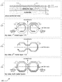
- FIG. 1 shows a layout of an inductor in accordance with an embodiment of the present invention.
- FIG. 2 shows a flow diagram in accordance with an embodiment of the present invention.
- the present invention relates to inductors. While the specification describes several example embodiments of the invention considered favorable modes of practicing the invention, it should be understood that the invention can be implemented in many ways and is not limited to the particular examples described below or to the particular manner in which any features of such examples are implemented. In other instances, well-known details are not shown or described to avoid obscuring aspects of the invention.
- FIG. 1 a layout of an inductor 100 is shown in FIG. 1 .
- the inductor 100 is fabricated on a silicon substrate 113 and includes a first coil of metal trace L 1 , a second coil of metal trace L 2 , and a third coil of metal trace L 3 .
- the first (second, third) coil of metal trace L 1 (L 2 , L 3 ) is simply referred to as L 1 (L 2 , L 3 ).
- L 1 and L 2 are placed within a first metal layer 111
- L 3 is placed within a second metal layer 112 .
- a dielectric slab 114 placed on top of the substrate 113 serves as a housing for securing the placement of L 1 , L 2 , and L 3 .
- L 1 is laid out to be substantially symmetrical with respect to a first axis
- L 2 is laid out to be a mirror image of L 1 with respect to a second axis.
- Both L 1 and L 2 are open loops and each of them has a narrow opening. For L 1 , the narrow opening is on the right hand side. For L 2 , the narrow opening is on the left hand side.
- L 3 is laid out to be substantially symmetrical with respect to both the first axis and the second axis. Unlike L 1 and L 2 , L 3 is a closed loop without an opening. As shown in a top view 140 of both metal layers, L 3 encloses a majority portion of both L 1 and L 2 from the top view perspective, although L 3 is placed in a different metal layer.
- I 1 I even +I odd
- I 2 I even ⁇ I odd
- I even is an even-mode current-mode signal that represents a symmetrical component in I 1 and I 2
- I odd is an odd-mode current-mode signal that represents an anti-symmetrical component in I 1 and I 2 .
- top view 130 of the second metal layer 112 Let a current following along L 3 in a clockwise direction be I 3 . Now refer to the top view 140 of both metal layers, along with referring to the aforementioned definitions of I 1 , I 2 , I 3 , I even , and I odd . According to Lenz law, an increase of I 1 will lead to an increase of I 3 due to a common magnetic flux shared by both L 1 and L 3 . On the other hand, an increase of I 2 will lead to a decrease of I 3 due to a common magnetic flux shared by both L 2 and L 3 .
- a user can use inductor 100 to perform a mode selection function.
- the existence of L 3 has no effect on I even , but a profound effect on I odd .
- the Lenz law will impede a change on I odd due to the existence of L 3 , since a change in a magnetic flux due to a change on I odd will lead to a change on I 3 that will oppose the change in the magnetic flux and thus undermine the change on I odd .
- the change on I odd will be greatly impeded. Therefore, the even mode signal I even can remain intact, while the odd mode signals I odd can be suppressed in the presence of L 3 .
- the undesired magnetic coupling from inductor 100 to an another inductor residing on the same silicon chip will be opposed by the undesired magnetic coupling from L 2 to said another inductor, since I 1 and I 2 are substantially the same (thanks to the aforementioned mode selection function) but they physically flow in opposite directions (i.e. one of them is clockwise, while the other one is counterclockwise).
- the inductor 100 therefore, can effectively mitigate the undesired magnetic coupling, and thus can be highly isolated from other inductances that coexist on the same silicon chip.
- both L 1 and L 2 are of a dimension of 160 ⁇ m by 160 ⁇ m; a trace width is 20 ⁇ m for both L 1 and L 2 ; a physical separation between L 1 and L 2 is 20 ⁇ m; the opening is 20 ⁇ m wide for both L 1 and L 2 ; a trace width of L 3 is 5 ⁇ m; a thickness of the first metal layer 111 is 3.2 ⁇ m; a thickness of the second metal layer 112 is 0.4 ⁇ m; a dielectric constant of the dielectric slab 114 is 4.1.
- the inductor 100 is laid out to be exactly symmetrical (i.e., L 1 is laid out to be exactly symmetrical with respect to the first axis, L 2 is laid out to be an exact mirror image of L 1 with respect to the second axis, and L 3 is laid out to be exactly symmetrical with respect to both the first axis and the second axis), an exact symmetry is desirable but not absolutely necessary.
- An inductor designer might choose to lay out the inductor 100 to be not highly symmetrical for whatever reason, but lack of a high degree of symmetry might lead to an appreciable degradation in the performance of aforementioned functions of mode selection and isolation. To have a reasonably good performance, the layout needs to be at least fairly symmetrical.
- the opening is deliberately configured to be on a side that is farthest away from the second axis.
- Such arrangement helps to minimize an undesired magnetic coupling from inductor 100 to another inductor located at a certain point along the first axis. If said another inductor is placed on the right (left) side of the second axis, the coupling from L 1 (L 2 ) to said another inductor will be greater than the coupling from L 2 (L 1 ) to said another inductor thanks to a shorter distance; the disparity between the two coupling degrades the isolation between inductor 100 and said another inductor.
- the disparity can be minimized.
- an opening of a coil does not generate a magnetic flux due to the absence of metal, and consequently cannot contribute to a magnetic coupling.
- said another inductor is placed on the right (left) side of the second axis, the coupling from L 1 (L 2 ) to said another inductor is minimized due to that the opening of L 1 (L 2 ), which contributes nothing to magnetic coupling, is located at a part of L 1 (L 2 ) that is closest to said another inductor.
- the part of inductor 100 that is closest to said another inductor and thus can potentially make a greatest contribution to the undesired coupling is deliberately deprived of its ability to generate a magnetic flux in the first place.
- a method comprises: (step 210 ) incorporating a first coil of metal trace, configured in an open loop topology, constructed in a first metal layer, and laid out to be fairly symmetrical with respect to a first axis; (step 220 ) incorporating a second coil of metal trace, configured in an open loop topology, constructed in the first metal layer, and laid out to be approximately a mirror image of the first coil of metal trace with respect with a second axis; and (step 230 ) incorporating a third coil of metal trace, configured in a closed loop topology, constructed in a second metal layer, and laid out to be approximately enclosing both the first coil of metal trace and the second coil of metal trace from a top view perspective.
Landscapes
- Engineering & Computer Science (AREA)
- Power Engineering (AREA)
- Coils Or Transformers For Communication (AREA)
- Semiconductor Integrated Circuits (AREA)
- Manufacturing & Machinery (AREA)
Abstract
Description
I 1 =I even +I odd (1)
I 2 =I even −I odd, (2)
I even≡(I 1 +I 2)/2 (3)
I odd≡(I 1 −I 2)/2. (4)
Claims (10)
Priority Applications (3)
| Application Number | Priority Date | Filing Date | Title |
|---|---|---|---|
| US15/481,691 US10522282B2 (en) | 2017-04-07 | 2017-04-07 | High isolation integrated inductor and method thereof |
| TW107110890A TWI685005B (en) | 2017-04-07 | 2018-03-29 | High isolation integrated inductor and manufacturing method thereof |
| CN201810283067.9A CN108695309B (en) | 2017-04-07 | 2018-04-02 | Highly isolated integrated inductor and method of making the same |
Applications Claiming Priority (1)
| Application Number | Priority Date | Filing Date | Title |
|---|---|---|---|
| US15/481,691 US10522282B2 (en) | 2017-04-07 | 2017-04-07 | High isolation integrated inductor and method thereof |
Publications (2)
| Publication Number | Publication Date |
|---|---|
| US20180294089A1 US20180294089A1 (en) | 2018-10-11 |
| US10522282B2 true US10522282B2 (en) | 2019-12-31 |
Family
ID=63711158
Family Applications (1)
| Application Number | Title | Priority Date | Filing Date |
|---|---|---|---|
| US15/481,691 Active 2037-09-16 US10522282B2 (en) | 2017-04-07 | 2017-04-07 | High isolation integrated inductor and method thereof |
Country Status (3)
| Country | Link |
|---|---|
| US (1) | US10522282B2 (en) |
| CN (1) | CN108695309B (en) |
| TW (1) | TWI685005B (en) |
Families Citing this family (7)
| Publication number | Priority date | Publication date | Assignee | Title |
|---|---|---|---|---|
| JP2020156180A (en) * | 2019-03-19 | 2020-09-24 | Tdk株式会社 | Coil unit, wireless power transmission device, wireless power receiving device, and wireless power transmission system |
| US12548707B2 (en) | 2019-09-11 | 2026-02-10 | Realtek Semiconductor Corporation | Inductor device |
| US12062480B2 (en) | 2019-09-11 | 2024-08-13 | Realtek Semiconductor Corporation | Inductor device |
| US11901399B2 (en) * | 2019-09-11 | 2024-02-13 | Realtek Semiconductor Corporation | Enhanced sensing coil for semiconductor device |
| US12488931B2 (en) | 2019-09-11 | 2025-12-02 | Realtek Semiconductor Corporation | Inductor device |
| TWI722946B (en) * | 2019-09-11 | 2021-03-21 | 瑞昱半導體股份有限公司 | Semiconductor device |
| US11869700B2 (en) | 2019-09-11 | 2024-01-09 | Realtek Semiconductor Corporation | Inductor device |
Citations (8)
| Publication number | Priority date | Publication date | Assignee | Title |
|---|---|---|---|---|
| US20060038635A1 (en) * | 2004-08-17 | 2006-02-23 | Dominick Richiuso | Integrated passive filter incorporating inductors and ESD protectors |
| US7327555B2 (en) | 2005-03-29 | 2008-02-05 | Realtek Semiconductor Corp. | Capacitor structure |
| US20080084255A1 (en) * | 2006-09-21 | 2008-04-10 | Samir El Rai | Integrated circuit arrangement and use of connecting lines |
| US7612645B2 (en) | 2005-10-12 | 2009-11-03 | Realtek Semiconductor Corp. | Integrated inductor |
| US20100033290A1 (en) * | 2007-06-08 | 2010-02-11 | Stats Chippac, Ltd. | Miniaturized Wide-Band Baluns for RF Applications |
| US20130249646A1 (en) * | 2012-03-23 | 2013-09-26 | Murata Manufacturing Co., Ltd. | Filter element |
| US20130278372A1 (en) * | 2012-04-20 | 2013-10-24 | Infineon Technologies Austria Ag | Semiconductor Component with Coreless Transformer |
| US20170012601A1 (en) | 2015-07-07 | 2017-01-12 | Realtek Semiconductor Corporation | Structures of planar transformer and balanced-to-unbalanced transformer |
Family Cites Families (4)
| Publication number | Priority date | Publication date | Assignee | Title |
|---|---|---|---|---|
| US7506712B2 (en) * | 2003-04-02 | 2009-03-24 | Yamaha Hatsudoki Kabushiki Kaisha | Off road vehicle with air intake system |
| TWI410986B (en) * | 2011-05-23 | 2013-10-01 | 矽品精密工業股份有限公司 | Symmetric differential inductor structure |
| US9543068B2 (en) * | 2014-06-17 | 2017-01-10 | Qualcomm Technologies International, Ltd. | Inductor structure and application thereof |
| CN106298190B (en) * | 2015-05-25 | 2019-03-15 | 瑞昱半导体股份有限公司 | Inductive device |
-
2017
- 2017-04-07 US US15/481,691 patent/US10522282B2/en active Active
-
2018
- 2018-03-29 TW TW107110890A patent/TWI685005B/en active
- 2018-04-02 CN CN201810283067.9A patent/CN108695309B/en active Active
Patent Citations (8)
| Publication number | Priority date | Publication date | Assignee | Title |
|---|---|---|---|---|
| US20060038635A1 (en) * | 2004-08-17 | 2006-02-23 | Dominick Richiuso | Integrated passive filter incorporating inductors and ESD protectors |
| US7327555B2 (en) | 2005-03-29 | 2008-02-05 | Realtek Semiconductor Corp. | Capacitor structure |
| US7612645B2 (en) | 2005-10-12 | 2009-11-03 | Realtek Semiconductor Corp. | Integrated inductor |
| US20080084255A1 (en) * | 2006-09-21 | 2008-04-10 | Samir El Rai | Integrated circuit arrangement and use of connecting lines |
| US20100033290A1 (en) * | 2007-06-08 | 2010-02-11 | Stats Chippac, Ltd. | Miniaturized Wide-Band Baluns for RF Applications |
| US20130249646A1 (en) * | 2012-03-23 | 2013-09-26 | Murata Manufacturing Co., Ltd. | Filter element |
| US20130278372A1 (en) * | 2012-04-20 | 2013-10-24 | Infineon Technologies Austria Ag | Semiconductor Component with Coreless Transformer |
| US20170012601A1 (en) | 2015-07-07 | 2017-01-12 | Realtek Semiconductor Corporation | Structures of planar transformer and balanced-to-unbalanced transformer |
Also Published As
| Publication number | Publication date |
|---|---|
| CN108695309A (en) | 2018-10-23 |
| CN108695309B (en) | 2021-04-23 |
| TWI685005B (en) | 2020-02-11 |
| US20180294089A1 (en) | 2018-10-11 |
| TW201837931A (en) | 2018-10-16 |
Similar Documents
| Publication | Publication Date | Title |
|---|---|---|
| US10522282B2 (en) | High isolation integrated inductor and method thereof | |
| TWI494957B (en) | Variable inductance | |
| US20190392980A1 (en) | Transformer device | |
| US7312685B1 (en) | Symmetrical inductor | |
| US20050237144A1 (en) | Planar inductance | |
| US8592943B2 (en) | Symmetrical center tap inductor structure | |
| KR20120125669A (en) | Stacked dual inductor structure | |
| US11328859B2 (en) | High isolation integrated inductor and method therof | |
| JPWO2008090995A1 (en) | Inductor | |
| KR20140026421A (en) | Symmetrical center tap inductor structure | |
| US6970064B2 (en) | Center-tap transformers in integrated circuits | |
| US20210297043A1 (en) | Integrated circuit including resonant circuit | |
| US8143696B2 (en) | Integrated circuit inductors with reduced magnetic coupling | |
| US20210065966A1 (en) | Inductor device | |
| JP2006179596A (en) | Semiconductor device | |
| JP2011254439A (en) | High-frequency circuit | |
| US10587312B1 (en) | Transmission interface having noise reduction function | |
| US20180254141A1 (en) | Integrated inductor and fabrication method thereof | |
| CN109950032B (en) | Variable inductance | |
| US11121692B2 (en) | Noise filter circuit | |
| US10943730B2 (en) | Single-ended inductor | |
| US11575359B2 (en) | Multi-port coupled inductor with interference suppression | |
| JP7589531B2 (en) | Inductor Configuration | |
| JP4884405B2 (en) | LC oscillator | |
| CN114171494B (en) | Diode and its semiconductor structure |
Legal Events
| Date | Code | Title | Description |
|---|---|---|---|
| AS | Assignment |
Owner name: REALTEK SEMICONDUCTOR CORP., TAIWAN Free format text: ASSIGNMENT OF ASSIGNORS INTEREST;ASSIGNORS:LEONG, POH-BOON;LIN, CHIA-LIANG (LEON);REEL/FRAME:041928/0916 Effective date: 20170405 |
|
| STPP | Information on status: patent application and granting procedure in general |
Free format text: RESPONSE TO NON-FINAL OFFICE ACTION ENTERED AND FORWARDED TO EXAMINER |
|
| STPP | Information on status: patent application and granting procedure in general |
Free format text: NON FINAL ACTION MAILED |
|
| STPP | Information on status: patent application and granting procedure in general |
Free format text: RESPONSE TO NON-FINAL OFFICE ACTION ENTERED AND FORWARDED TO EXAMINER |
|
| STPP | Information on status: patent application and granting procedure in general |
Free format text: NOTICE OF ALLOWANCE MAILED -- APPLICATION RECEIVED IN OFFICE OF PUBLICATIONS |
|
| STCF | Information on status: patent grant |
Free format text: PATENTED CASE |
|
| MAFP | Maintenance fee payment |
Free format text: PAYMENT OF MAINTENANCE FEE, 4TH YEAR, LARGE ENTITY (ORIGINAL EVENT CODE: M1551); ENTITY STATUS OF PATENT OWNER: LARGE ENTITY Year of fee payment: 4 |