US10510538B2 - Reducing EUV-induced material property changes - Google Patents
Reducing EUV-induced material property changes Download PDFInfo
- Publication number
- US10510538B2 US10510538B2 US15/499,715 US201715499715A US10510538B2 US 10510538 B2 US10510538 B2 US 10510538B2 US 201715499715 A US201715499715 A US 201715499715A US 10510538 B2 US10510538 B2 US 10510538B2
- Authority
- US
- United States
- Prior art keywords
- thickness
- dielectric layer
- layer
- thermal treatment
- compressive stress
- Prior art date
- Legal status (The legal status is an assumption and is not a legal conclusion. Google has not performed a legal analysis and makes no representation as to the accuracy of the status listed.)
- Active
Links
Images


Classifications
-
- H—ELECTRICITY
- H10—SEMICONDUCTOR DEVICES; ELECTRIC SOLID-STATE DEVICES NOT OTHERWISE PROVIDED FOR
- H10P—GENERIC PROCESSES OR APPARATUS FOR THE MANUFACTURE OR TREATMENT OF DEVICES COVERED BY CLASS H10
- H10P76/00—Manufacture or treatment of masks on semiconductor bodies, e.g. by lithography or photolithography
- H10P76/20—Manufacture or treatment of masks on semiconductor bodies, e.g. by lithography or photolithography of masks comprising organic materials
- H10P76/204—Manufacture or treatment of masks on semiconductor bodies, e.g. by lithography or photolithography of masks comprising organic materials of organic photoresist masks
- H10P76/2041—Photolithographic processes
-
- H01L21/0274—
-
- H—ELECTRICITY
- H10—SEMICONDUCTOR DEVICES; ELECTRIC SOLID-STATE DEVICES NOT OTHERWISE PROVIDED FOR
- H10P—GENERIC PROCESSES OR APPARATUS FOR THE MANUFACTURE OR TREATMENT OF DEVICES COVERED BY CLASS H10
- H10P14/00—Formation of materials, e.g. in the shape of layers or pillars
- H10P14/60—Formation of materials, e.g. in the shape of layers or pillars of insulating materials
- H10P14/69—Inorganic materials
- H10P14/692—Inorganic materials composed of oxides, glassy oxides or oxide-based glasses
- H10P14/6921—Inorganic materials composed of oxides, glassy oxides or oxide-based glasses containing silicon
- H10P14/6922—Inorganic materials composed of oxides, glassy oxides or oxide-based glasses containing silicon the material containing Si, O and at least one of H, N, C, F or other non-metal elements, e.g. SiOC, SiOC:H or SiONC
-
- C—CHEMISTRY; METALLURGY
- C23—COATING METALLIC MATERIAL; COATING MATERIAL WITH METALLIC MATERIAL; CHEMICAL SURFACE TREATMENT; DIFFUSION TREATMENT OF METALLIC MATERIAL; COATING BY VACUUM EVAPORATION, BY SPUTTERING, BY ION IMPLANTATION OR BY CHEMICAL VAPOUR DEPOSITION, IN GENERAL; INHIBITING CORROSION OF METALLIC MATERIAL OR INCRUSTATION IN GENERAL
- C23C—COATING METALLIC MATERIAL; COATING MATERIAL WITH METALLIC MATERIAL; SURFACE TREATMENT OF METALLIC MATERIAL BY DIFFUSION INTO THE SURFACE, BY CHEMICAL CONVERSION OR SUBSTITUTION; COATING BY VACUUM EVAPORATION, BY SPUTTERING, BY ION IMPLANTATION OR BY CHEMICAL VAPOUR DEPOSITION, IN GENERAL
- C23C14/00—Coating by vacuum evaporation, by sputtering or by ion implantation of the coating forming material
- C23C14/22—Coating by vacuum evaporation, by sputtering or by ion implantation of the coating forming material characterised by the process of coating
- C23C14/48—Ion implantation
-
- C—CHEMISTRY; METALLURGY
- C23—COATING METALLIC MATERIAL; COATING MATERIAL WITH METALLIC MATERIAL; CHEMICAL SURFACE TREATMENT; DIFFUSION TREATMENT OF METALLIC MATERIAL; COATING BY VACUUM EVAPORATION, BY SPUTTERING, BY ION IMPLANTATION OR BY CHEMICAL VAPOUR DEPOSITION, IN GENERAL; INHIBITING CORROSION OF METALLIC MATERIAL OR INCRUSTATION IN GENERAL
- C23C—COATING METALLIC MATERIAL; COATING MATERIAL WITH METALLIC MATERIAL; SURFACE TREATMENT OF METALLIC MATERIAL BY DIFFUSION INTO THE SURFACE, BY CHEMICAL CONVERSION OR SUBSTITUTION; COATING BY VACUUM EVAPORATION, BY SPUTTERING, BY ION IMPLANTATION OR BY CHEMICAL VAPOUR DEPOSITION, IN GENERAL
- C23C16/00—Chemical coating by decomposition of gaseous compounds, without leaving reaction products of surface material in the coating, i.e. chemical vapour deposition [CVD] processes
- C23C16/22—Chemical coating by decomposition of gaseous compounds, without leaving reaction products of surface material in the coating, i.e. chemical vapour deposition [CVD] processes characterised by the deposition of inorganic material, other than metallic material
- C23C16/30—Deposition of compounds, mixtures or solid solutions, e.g. borides, carbides, nitrides
-
- C—CHEMISTRY; METALLURGY
- C23—COATING METALLIC MATERIAL; COATING MATERIAL WITH METALLIC MATERIAL; CHEMICAL SURFACE TREATMENT; DIFFUSION TREATMENT OF METALLIC MATERIAL; COATING BY VACUUM EVAPORATION, BY SPUTTERING, BY ION IMPLANTATION OR BY CHEMICAL VAPOUR DEPOSITION, IN GENERAL; INHIBITING CORROSION OF METALLIC MATERIAL OR INCRUSTATION IN GENERAL
- C23C—COATING METALLIC MATERIAL; COATING MATERIAL WITH METALLIC MATERIAL; SURFACE TREATMENT OF METALLIC MATERIAL BY DIFFUSION INTO THE SURFACE, BY CHEMICAL CONVERSION OR SUBSTITUTION; COATING BY VACUUM EVAPORATION, BY SPUTTERING, BY ION IMPLANTATION OR BY CHEMICAL VAPOUR DEPOSITION, IN GENERAL
- C23C16/00—Chemical coating by decomposition of gaseous compounds, without leaving reaction products of surface material in the coating, i.e. chemical vapour deposition [CVD] processes
- C23C16/44—Chemical coating by decomposition of gaseous compounds, without leaving reaction products of surface material in the coating, i.e. chemical vapour deposition [CVD] processes characterised by the method of coating
- C23C16/455—Chemical coating by decomposition of gaseous compounds, without leaving reaction products of surface material in the coating, i.e. chemical vapour deposition [CVD] processes characterised by the method of coating characterised by the method used for introducing gases into reaction chamber or for modifying gas flows in reaction chamber
- C23C16/45523—Pulsed gas flow or change of composition over time
- C23C16/45525—Atomic layer deposition [ALD]
-
- C—CHEMISTRY; METALLURGY
- C23—COATING METALLIC MATERIAL; COATING MATERIAL WITH METALLIC MATERIAL; CHEMICAL SURFACE TREATMENT; DIFFUSION TREATMENT OF METALLIC MATERIAL; COATING BY VACUUM EVAPORATION, BY SPUTTERING, BY ION IMPLANTATION OR BY CHEMICAL VAPOUR DEPOSITION, IN GENERAL; INHIBITING CORROSION OF METALLIC MATERIAL OR INCRUSTATION IN GENERAL
- C23C—COATING METALLIC MATERIAL; COATING MATERIAL WITH METALLIC MATERIAL; SURFACE TREATMENT OF METALLIC MATERIAL BY DIFFUSION INTO THE SURFACE, BY CHEMICAL CONVERSION OR SUBSTITUTION; COATING BY VACUUM EVAPORATION, BY SPUTTERING, BY ION IMPLANTATION OR BY CHEMICAL VAPOUR DEPOSITION, IN GENERAL
- C23C16/00—Chemical coating by decomposition of gaseous compounds, without leaving reaction products of surface material in the coating, i.e. chemical vapour deposition [CVD] processes
- C23C16/44—Chemical coating by decomposition of gaseous compounds, without leaving reaction products of surface material in the coating, i.e. chemical vapour deposition [CVD] processes characterised by the method of coating
- C23C16/48—Chemical coating by decomposition of gaseous compounds, without leaving reaction products of surface material in the coating, i.e. chemical vapour deposition [CVD] processes characterised by the method of coating by irradiation, e.g. photolysis, radiolysis, particle radiation
- C23C16/483—Chemical coating by decomposition of gaseous compounds, without leaving reaction products of surface material in the coating, i.e. chemical vapour deposition [CVD] processes characterised by the method of coating by irradiation, e.g. photolysis, radiolysis, particle radiation using coherent light, UV to IR, e.g. lasers
-
- C—CHEMISTRY; METALLURGY
- C23—COATING METALLIC MATERIAL; COATING MATERIAL WITH METALLIC MATERIAL; CHEMICAL SURFACE TREATMENT; DIFFUSION TREATMENT OF METALLIC MATERIAL; COATING BY VACUUM EVAPORATION, BY SPUTTERING, BY ION IMPLANTATION OR BY CHEMICAL VAPOUR DEPOSITION, IN GENERAL; INHIBITING CORROSION OF METALLIC MATERIAL OR INCRUSTATION IN GENERAL
- C23C—COATING METALLIC MATERIAL; COATING MATERIAL WITH METALLIC MATERIAL; SURFACE TREATMENT OF METALLIC MATERIAL BY DIFFUSION INTO THE SURFACE, BY CHEMICAL CONVERSION OR SUBSTITUTION; COATING BY VACUUM EVAPORATION, BY SPUTTERING, BY ION IMPLANTATION OR BY CHEMICAL VAPOUR DEPOSITION, IN GENERAL
- C23C16/00—Chemical coating by decomposition of gaseous compounds, without leaving reaction products of surface material in the coating, i.e. chemical vapour deposition [CVD] processes
- C23C16/44—Chemical coating by decomposition of gaseous compounds, without leaving reaction products of surface material in the coating, i.e. chemical vapour deposition [CVD] processes characterised by the method of coating
- C23C16/50—Chemical coating by decomposition of gaseous compounds, without leaving reaction products of surface material in the coating, i.e. chemical vapour deposition [CVD] processes characterised by the method of coating using electric discharges
-
- C—CHEMISTRY; METALLURGY
- C23—COATING METALLIC MATERIAL; COATING MATERIAL WITH METALLIC MATERIAL; CHEMICAL SURFACE TREATMENT; DIFFUSION TREATMENT OF METALLIC MATERIAL; COATING BY VACUUM EVAPORATION, BY SPUTTERING, BY ION IMPLANTATION OR BY CHEMICAL VAPOUR DEPOSITION, IN GENERAL; INHIBITING CORROSION OF METALLIC MATERIAL OR INCRUSTATION IN GENERAL
- C23C—COATING METALLIC MATERIAL; COATING MATERIAL WITH METALLIC MATERIAL; SURFACE TREATMENT OF METALLIC MATERIAL BY DIFFUSION INTO THE SURFACE, BY CHEMICAL CONVERSION OR SUBSTITUTION; COATING BY VACUUM EVAPORATION, BY SPUTTERING, BY ION IMPLANTATION OR BY CHEMICAL VAPOUR DEPOSITION, IN GENERAL
- C23C16/00—Chemical coating by decomposition of gaseous compounds, without leaving reaction products of surface material in the coating, i.e. chemical vapour deposition [CVD] processes
- C23C16/56—After-treatment
-
- H01L21/02274—
-
- H01L21/0228—
-
- H01L21/02296—
-
- H—ELECTRICITY
- H10—SEMICONDUCTOR DEVICES; ELECTRIC SOLID-STATE DEVICES NOT OTHERWISE PROVIDED FOR
- H10P—GENERIC PROCESSES OR APPARATUS FOR THE MANUFACTURE OR TREATMENT OF DEVICES COVERED BY CLASS H10
- H10P14/00—Formation of materials, e.g. in the shape of layers or pillars
- H10P14/60—Formation of materials, e.g. in the shape of layers or pillars of insulating materials
- H10P14/63—Formation of materials, e.g. in the shape of layers or pillars of insulating materials characterised by the formation processes
- H10P14/6326—Deposition processes
- H10P14/6328—Deposition from the gas or vapour phase
- H10P14/6334—Deposition from the gas or vapour phase using decomposition or reaction of gaseous or vapour phase compounds, i.e. chemical vapour deposition
- H10P14/6336—Deposition from the gas or vapour phase using decomposition or reaction of gaseous or vapour phase compounds, i.e. chemical vapour deposition in the presence of a plasma [PECVD]
-
- H—ELECTRICITY
- H10—SEMICONDUCTOR DEVICES; ELECTRIC SOLID-STATE DEVICES NOT OTHERWISE PROVIDED FOR
- H10P—GENERIC PROCESSES OR APPARATUS FOR THE MANUFACTURE OR TREATMENT OF DEVICES COVERED BY CLASS H10
- H10P14/00—Formation of materials, e.g. in the shape of layers or pillars
- H10P14/60—Formation of materials, e.g. in the shape of layers or pillars of insulating materials
- H10P14/63—Formation of materials, e.g. in the shape of layers or pillars of insulating materials characterised by the formation processes
- H10P14/6326—Deposition processes
- H10P14/6328—Deposition from the gas or vapour phase
- H10P14/6334—Deposition from the gas or vapour phase using decomposition or reaction of gaseous or vapour phase compounds, i.e. chemical vapour deposition
- H10P14/6339—Deposition from the gas or vapour phase using decomposition or reaction of gaseous or vapour phase compounds, i.e. chemical vapour deposition deposition by cyclic CVD, e.g. ALD, ALE or pulsed CVD
-
- H—ELECTRICITY
- H10—SEMICONDUCTOR DEVICES; ELECTRIC SOLID-STATE DEVICES NOT OTHERWISE PROVIDED FOR
- H10P—GENERIC PROCESSES OR APPARATUS FOR THE MANUFACTURE OR TREATMENT OF DEVICES COVERED BY CLASS H10
- H10P14/00—Formation of materials, e.g. in the shape of layers or pillars
- H10P14/60—Formation of materials, e.g. in the shape of layers or pillars of insulating materials
- H10P14/65—Formation of materials, e.g. in the shape of layers or pillars of insulating materials characterised by treatments performed before or after the formation of the materials
- H10P14/6516—Formation of materials, e.g. in the shape of layers or pillars of insulating materials characterised by treatments performed before or after the formation of the materials of treatments performed after formation of the materials
- H10P14/6536—Formation of materials, e.g. in the shape of layers or pillars of insulating materials characterised by treatments performed before or after the formation of the materials of treatments performed after formation of the materials by exposure to radiation, e.g. visible light
- H10P14/6538—Formation of materials, e.g. in the shape of layers or pillars of insulating materials characterised by treatments performed before or after the formation of the materials of treatments performed after formation of the materials by exposure to radiation, e.g. visible light by exposure to UV light
-
- H—ELECTRICITY
- H10—SEMICONDUCTOR DEVICES; ELECTRIC SOLID-STATE DEVICES NOT OTHERWISE PROVIDED FOR
- H10P—GENERIC PROCESSES OR APPARATUS FOR THE MANUFACTURE OR TREATMENT OF DEVICES COVERED BY CLASS H10
- H10P50/00—Etching of wafers, substrates or parts of devices
- H10P50/73—Etching of wafers, substrates or parts of devices using masks for insulating materials
-
- H—ELECTRICITY
- H10—SEMICONDUCTOR DEVICES; ELECTRIC SOLID-STATE DEVICES NOT OTHERWISE PROVIDED FOR
- H10W—GENERIC PACKAGES, INTERCONNECTIONS, CONNECTORS OR OTHER CONSTRUCTIONAL DETAILS OF DEVICES COVERED BY CLASS H10
- H10W20/00—Interconnections in chips, wafers or substrates
- H10W20/01—Manufacture or treatment
- H10W20/071—Manufacture or treatment of dielectric parts thereof
- H10W20/093—Manufacture or treatment of dielectric parts thereof by modifying materials of the dielectric parts
- H10W20/097—Manufacture or treatment of dielectric parts thereof by modifying materials of the dielectric parts by thermally treating
Definitions
- NGL Next generation lithography
- EUVL extreme ultraviolet
- EUVL electron projection lithography
- IPL ion projection lithography
- X-ray lithography X-ray lithography
- FIGS. 1-3 representatively illustrate manufacturing stages for a region of a semiconductor wafer, in accordance with an embodiment.
- FIG. 4 representatively illustrates thermal treatment of a dielectric layer before extreme ultraviolet (EUV) exposure attendant to extreme ultraviolet lithography (EUVL) processing, in accordance with an embodiment.
- EUV extreme ultraviolet lithography
- FIGS. 5-8 representatively illustrate manufacturing stages for a region of a semiconductor wafer, in accordance with another embodiment.
- FIG. 9 representatively illustrates thermal treatment of a dielectric layer before EUV exposure attendant to EUVL processing, in accordance with another embodiment.
- FIG. 10 representatively illustrates a sparsely-(or less-densely-) packed region of SiOC material prior to thermal treatment in accordance with an embodiment.
- FIG. 11 representatively illustrates a more-densely-packed region of SiOC material after thermal treatment, in accordance with an embodiment.
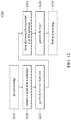
- FIG. 12 is a process flow diagram representatively illustrating a method for preventing or otherwise reducing lithography-induced material property changes to a material layer, in accordance with an embodiment.
- FIG. 13 is a process flow diagram representatively illustrating a method for preventing, or otherwise reducing, EUVL-induced material property changes to a dielectric layer, in accordance with an embodiment.
- FIG. 14 is a process flow diagram representatively illustrating a method for preventing, or otherwise reducing, EUVL-induced thickness shrinkage of a dielectric layer, in accordance with an embodiment.
- Spatially relative terms such as “beneath,” “below,” “lower,” “under,” “above,” “upper,” “over,” “adjacent,” “interposing,” and contextual variants thereof, may be used herein for ease of description to describe an element or feature in relationship to other elements or features representatively illustrated in the Figures. Spatially relative terms are intended to encompass different orientations of a device in use or operation, in addition to orientations representatively illustrated in the Figures. Devices or structures may be otherwise oriented (e.g., rotated 90 degrees, or at other orientations) with spatially relative descriptors used herein being interpreted accordingly.
- Optical lithography processes are used to form device features of integrated circuits on wafers.
- a typical optical lithography process involves applying a photoresist and defining patterns in the photoresist. Transparent or opaque portions of the lithography mask define the pattern in the photoresist.
- the patterns in the photoresist may then be transferred to underlying features with etching, where the patterned photoresist is used as an etching mask. After etching, the patterned photoresist is removed.
- optical proximity effects pose a greater challenge for transferring patterns from a photolithography mask to a wafer.
- optical proximity effects may cause adjacent features to short between one another.
- Double-patterning technology has been introduced for enhancing feature definition to address such challenges.
- Two-pattern-two-etch (2P2E) is one such technology.
- closely-spaced features are separated into two (or more) lithography masks, with separate lithography masks being used to expose the same photoresist or different photoresists such that patterns for closely-spaced features may be subsequently transferred to a same layer.
- distances between features are increased over the distances between the features in the otherwise single-pattern mask so as to be suitably larger than the wavelength of electromagnetic radiation used to expose the pattern.
- the resolution of composite imaging is effectively doubled. Consequently, distances in multi-patterning lithography masks are typically greater than the threshold distances for the onset of optical proximity effects, and hence, substantially reduce challenges associated with such effects.
- Embodiments disclosed herein generally relate to the field of fabricating semiconductor devices with closely-spaced device elements, and more particularly, to methods of stabilizing material of a semiconductor device layer (e.g., a dielectric layer) prior to imaging/patterning with extreme ultraviolet (EUV) lithography (EUVL).
- a semiconductor device layer e.g., a dielectric layer
- EUVL extreme ultraviolet lithography
- Representative embodiments provide treatment processes to strengthen whole bulk film quality for improved heat and radiation resistance, as well as to relieve, or otherwise reduce, film stress for improved film stack assembly.
- a workpiece may comprise a device wafer that includes active devices (e.g., transistors, diodes, and/or the like), and optional passive devices (e.g., capacitors, inductors, resistors, and/or the like).
- the transistors may comprise fin field-effect transistors (FinFETs).
- the transistors may also comprise gate-all-around (GAA) structures. Methods of fabricating transistors, FinFETs, and GAA structures are well known in the art, and will therefore not be discussed here at length in the interest of concision and clarity of description.
- FIG. 1 representatively illustrates a region of a workpiece (e.g., a semiconductor wafer) in accordance with some embodiments.
- the workpiece may include a semiconductor substrate 110 and features formed over a surface of semiconductor substrate 110 .
- the substrate may comprise a silicon substrate.
- the substrate may comprise one or more other suitable elemental semiconductors (e.g., diamond or germanium), a suitable compound semiconductor (e.g., gallium arsenide, silicon carbide, indium arsenide, or indium phosphide), or a suitable alloy semiconductor (e.g., silicon germanium carbide, gallium arsenic phosphide, or gallium indium phosphide).
- suitable elemental semiconductors e.g., diamond or germanium
- a suitable compound semiconductor e.g., gallium arsenide, silicon carbide, indium arsenide, or indium phosphide
- a suitable alloy semiconductor e.g., silicon germanium carbide, gallium ar
- Substrate 110 may further comprise other features, such as various doped regions, a buried layer, an epitaxy layer, and/or insulating regions (not illustrated).
- Substrate 110 may be a silicon on insulator (SOI) or silicon on sapphire.
- substrate 110 may comprise a doped epitaxial layer, a gradient semiconductor layer, and/or may further include a semiconductor layer overlying another semiconductor layer of a different type, such as a silicon layer on a silicon germanium layer.
- a compound semiconductor substrate may comprise a multilayer silicon structure, or a silicon substrate may include a multilayer compound semiconductor structure.
- Shallow trench isolation (STI) regions may be formed in semiconductor substrate 110 to isolate active regions (e.g., transistors) in semiconductor substrate 110 .
- Through-vias may be formed to extend into semiconductor substrate 110 to electrically couple device features on opposing sides of the workpiece.
- dielectric layer 220 may be formed over substrate 110 .
- dielectric layer 220 may be used as a contact etch stop layer (CESL).
- Dielectric layer 220 may comprise an oxide, a nitride, a silicon-carbon based material, a carbon-doped oxide, and/or combinations thereof.
- dielectric layer 220 may comprise one or more of SiOC, SiN, SiON, SiOCN, SiO, or the like.
- Fabrication methods to form dielectric layer 220 may include plasma enhanced chemical vapor deposition (PECVD), or other methods such as high-density plasma CVD (HDPCVD), atomic layer CVD (ALCVD), and/or the like.
- Dielectric layer 220 may be a single layer or may include more than one layer.
- dielectric layer 330 may be formed over dielectric layer 220 .
- dielectric layer 330 may be formed of a low-k dielectric material.
- Dielectric layer 330 may be formed using one or more materials selected from the same or substantially similar materials forming dielectric layer 220 . When selected from similar materials, the materials of dielectric layer 220 and dielectric layer 330 may be the same as or different from each other.
- Dielectric layer 330 may be formed using one or more processes selected from the same or substantially similar processes forming dielectric layer 220 . When selected from similar processes, the processes forming dielectric layer 220 and dielectric layer 330 may be the same as or different from each other.
- dielectric layer 330 may be formed of a low-k dielectric material having a dielectric constant (k-value) lower than about 3.0, lower than about 2.5, or lower than about 1.9.
- Low-k dielectric layer 330 may be formed of Black Diamond® (a registered trademark of Applied Materials, Santa Clara, Calif., USA), a carbon-containing low-k dielectric material, hydrogen silsesquioxane (HSQ), methylsilsesquioxane (MSQ), or the like.
- formation of dielectric layer 330 may include deposition of a porogen-containing dielectric material followed by a curing process to drive out porogen, thereby forming a layer of porous dielectric material.
- dielectric layer 220 may not be present, and therefore not interposed between substrate 110 and dielectric layer 330 .
- EUV exposure attendant to patterning dielectric layer 330 may comprise extreme ultraviolet light having a wavelength of about 13.5 nm.
- Use of extreme ultraviolet light e.g., in the above-described processing context
- immersion UV e.g., employing wavelengths of 193 nm or 199 nm
- the decreased wavelength associated with EUV corresponds to an increased magnitude and depth of energy deposition. With increasing energy, it has been observed that relatively deeply-disposed layers may experience damage or changes to their material properties upon exposure to extreme ultraviolet light.
- EUV exposure may cause a layer thickness shrinkage of about 27%.
- thermal treatment processes are provided to prevent or otherwise reduce material property changes attendant to EUVL pattern imaging.
- dielectric layer 330 has an as-deposited thickness ⁇ .
- Wafer region 400 is subjected to thermal treatment 450 to produce thermally treated wafer region 400 ′.
- thermally treated wafer region 400 ′ comprises thermally treated dielectric layer 330 ′ having a post-treatment thickness ⁇ ′.
- Thermally treated wafer region 400 ′ may thereafter be exposed to EUV radiation attendant to EUVL patterning, where EUV exposure of thermally treated dielectric layer 330 ′ may induce a layer thickness change attendant to EUV exposure.
- ⁇ ′ is less than ⁇
- a post-EUV-exposure thickness of thermally treated dielectric layer 330 ′ may be less than ⁇ ′.
- Same or similar thickness shrinkage considerations may apply for dielectric layer 220 .
- the as-deposited thickness ⁇ may be about 19.24 nm
- the post-treatment thickness ⁇ ′ may be about 18.91 nm
- the post-EUV-exposure thickness may be about 17.45 nm.
- the as-deposited thickness ⁇ may be about 19.3 nm
- the post-treatment thickness ⁇ ′ may be about 19.0 nm
- the post-EUV-exposure thickness may be about 18 nm.
- a ratio of the post-treatment thickness ⁇ ′ to the as-deposited thickness ⁇ may be about 0.98 (e.g., the post-treatment thickness ⁇ ′ being about 98% the value of the as-deposited thickness ⁇ ), and a ratio of the post-EUV-exposure thickness to the post-treatment thickness ⁇ ′ may be about 0.95 (e.g., the post-EUV-exposure thickness being about 95% the value of the post-treatment thickness ⁇ ′). In yet other embodiments, a ratio of the post-EUV-exposure thickness to the as-deposited thickness ⁇ may be about 0.90 (e.g., the post-EUV-exposure thickness being about 90% the value of the as-deposited thickness ⁇ ).
- thermal treatment 450 may comprise heating wafer region 400 to a temperature of up to about 400° C.
- wafer region 400 may be heated to a temperature of about 250° C. for a duration of time between about 30 minutes and about 40 minutes.
- wafer region 400 may be heated to a temperature of about 400° C. for a duration of time between about 10 minutes and about 15 minutes.
- thermal treatment 450 may comprise one or more baking or annealing processes or stages.
- thermal treatment 450 may comprise one or more ultraviolet (UV) radiation treatments (e.g., with wavelengths longer than EUV wavelengths), ion implantations, ion bombardments, plasma treatments, surface baking treatments, surface coating treatments, surface ashing treatments, pulsed laser treatments, or combinations thereof.
- UV radiation treatments e.g., with wavelengths longer than EUV wavelengths
- ion implantations e.g., with wavelengths longer than EUV wavelengths
- ion bombardments plasma treatments
- surface baking treatments e.g., surface coating treatments, surface ashing treatments, pulsed laser treatments, or combinations thereof.
- one or more material layers to be thermally treated prior to EUVL patterning may be thermally treated at any stage of device fabrication.
- Thermal treatment 450 may comprise exposing wafer region 400 to ultraviolet light comprising one or more wavelengths between about 200 nm and about 400 nm.
- wafer region 400 may be exposed to UV light comprising one or more wavelengths between about 200 nm and about 400 nm for a duration of time of about 2 minutes.
- a commercially available UV bulb such as a fusion-type UV bulb (e.g., available from Haraeus Noblelight America, LLC, Plainview, N.Y., USA) may be used to perform thermal treatment 450 .
- Other wavelengths and durations may be alternatively or sequentially employed.
- thermal treatment 450 may comprise one or more UV exposure stages or processes.
- one or more material layers to be thermally treated prior to EUV exposure may be thermally treated at any phase of semiconductor device fabrication.
- a region of a workpiece may include a semiconductor substrate 510 and features formed over a surface of semiconductor substrate 510 .
- substrate 510 may have a same or similar composition as substrate 110 .
- Shallow trench isolation (STI) regions may be formed in substrate 510 to isolate active regions (e.g., transistors) in substrate 510 .
- Through-vias may be formed to extend into substrate 510 and electrically couple device features on opposing sides of the workpiece.
- dielectric layer 620 may be formed over substrate 510 .
- Dielectric layer 620 may have a same or similar composition as dielectric layer 220 .
- Dielectric layer 620 may be formed by a same or similar process as dielectric layer 220 .
- Dielectric layer 620 may be a single layer or may include more than one layer.
- dielectric layer 730 may be formed over dielectric layer 620 .
- Dielectric layer 730 may be formed of a same or similar composition as dielectric layer 330 , and dielectric layer 730 may be formed by a same or similar process as dielectric layer 330 .
- material layer 880 may be deposited over dielectric layer 730 prior to EUV photolithographic processing.
- material layer 880 may comprise one or more layers comprising one or more material compositions known in the art of semiconductor device manufacture.
- dielectric layer 730 has an as-deposited thickness ⁇ .
- Wafer region 900 is subjected to thermal treatment 450 to produce thermally treated wafer region 900 ′.
- thermally treated wafer region 900 ′ comprises thermally treated dielectric layer 730 ′ having a post-treatment thickness ⁇ ′.
- Thermally treated wafer region 900 ′ may thereafter be exposed to EUV radiation attendant to EUVL photolithographic patterning, where EUV exposure of thermally treated dielectric layer 730 ′ may induce a layer thickness change attendant to EUV exposure.
- ⁇ ′ may be less than ⁇
- a post-EUV-exposure thickness of thermally treated dielectric layer 730 ′ may be less than ⁇ ′.
- Same or similar thickness shrinkage considerations may apply to dielectric layer 620 and/or material layer 880 .
- the as-deposited thickness ⁇ may be about 19.24 nm
- the post-treatment thickness ⁇ ′ may be about 18.91 nm
- the post-EUV-exposure thickness may be about 17.45 nm.
- the as-deposited thickness ⁇ may be about 19.3 nm
- the post-treatment thickness ⁇ ′ may be about 19.0 nm
- the post-EUV-exposure thickness may be about 18 nm.
- a ratio of the post-treatment thickness ⁇ ′ to the as-deposited thickness ⁇ may be about 0.98 (e.g., the post-treatment thickness ⁇ ′ being about 98% the value of the as-deposited thickness ⁇ ), and a ratio of the post-EUV-exposure thickness to the post-treatment thickness ⁇ ′ may be about 0.95 (e.g., the post-EUV-exposure thickness being about 95% the value of the post-treatment thickness ⁇ ′). In yet other embodiments, a ratio of the post-EUV-exposure thickness to the as-deposited thickness ⁇ may be about 0.90 (e.g., the post-EUV-exposure thickness being about 90% the value of the as-deposited thickness ⁇ ).
- a tri-layer may be formed over dielectric layer 330 or dielectric layer 730 .
- the tri-layer may include a bottom layer, a middle layer, and an upper layer.
- the middle layer may be disposed over the bottom layer, and the upper layer may be disposed over the middle layer.
- the bottom layer and upper layer may be formed of one or more photoresist materials.
- the middle layer may be formed of a silicon-containing material, which may be a nitride (e.g., SiN), an oxynitride (e.g., SiON), an oxide (e.g., SiO), a carbide (e.g., SiOC), or the like.
- the middle layer generally has a relatively high etch selectivity as compared to the upper layer and the bottom layer. Accordingly, the upper layer may be used as an etching mask for patterning the middle layer. Similarly, the middle layer may be used as an etching mask for patterning the bottom layer.
- an optional antireflective layer (ARL) or nitrogen-free ARL (NFARL) may be deposited over dielectric layer 330 or dielectric layer 730 with, e.g., PECVD.
- Thermal treatment 450 may comprise plural stages. Where thermal treatment 450 comprises more than one stage, various sequencing permutations among and between thermal treatment stages are possible (e.g., alternation or interleaving of heat treatment stages and UV treatment stages).
- a material layer may be thermally treated to densify its structure prior to deposition of one or more layers on or overlying the material layer to be thermally treated. In other embodiments, a material layer may be thermally treated to densify its structure after deposition of one or more other layers on or overlying the material layer to be thermally treated.
- FIG. 10 illustrates a sparsely-packed (or less-densely-packed) arrangement of SiOC material 1000 , in accordance with a representative embodiment.
- some regions (or portions) of SiOC material 1000 may be spatially separated from other regions (or portions) of SiOC material 1000 .
- there may be a relatively low population of closed ring structures (not illustrated in FIG. 10 ).
- FIG. 10 omits depiction of hydrogen atoms and bonds to hydrogen atoms, in accordance with standard practice in the art.
- FIG. 11 illustrates formation of more-densely-packed SiOC material 1100 after application of one or more thermal treatments 450 applied to sparsely-packed SiOC material 1000 , in accordance with representative embodiments.
- thermal treatment(s) 450 is/are applied to sparsely-packed SiOC material 1000 , a more compact Si—O—Si structure is formed resulting from a densified (or more-densely-packed) bonding structure of SiOC material 1100 .
- More-densely-packed SiOC material 1100 will generally exhibit a stronger Si—O—Si bond network with fewer dangling bonds, as compared to sparsely-packed SiOC material 1000 .
- thermal treatment processes may extend densification of the three-dimensional Si—O—Si bond network, thereby reducing the population of dangling bonds otherwise appearing in the structure of sparsely-packed SiOC material 1000 . Additionally, there may be a relatively higher population of closed ring structures in more-densely-packed SiOC material 1100 as compared to sparsely-packed SiOC material 1000 . As representatively illustrated, FIG. 11 also omits depiction of hydrogen atoms and bonds to hydrogen atoms, in accordance with standard practice in the art.
- Reduction of dangling bonds generally contributes to better material layer and bulk film quality.
- Better material layer and bulk film quality generally provides improved resistance to heat-induced and radiation-induced changes in layer/film quality during subsequent EUV photolithographic processing.
- FIG. 10 and FIG. 11 representatively illustrate densification of SiOC material
- various other materials may be similarly processed to reduce the occurrence of dangling bonds or otherwise improve material layer and/or bulk film quality.
- SiOCN, SiN, SiON, SiO, and/or the like may be similarly thermally treated 450 to similarly densify their respective bond network structures.
- FIG. 12 representatively illustrates a method for preventing, or otherwise reducing, electromagnetic radiation-induced property changes to a material layer (e.g., dielectric layer 330 , dielectric layer 220 , dielectric layer 730 , dielectric layer 620 ) attendant to photolithographic patterning, in accordance with an embodiment.
- the method optionally begins with pre-processing step 1210 .
- Pre-processing step 1210 may include various optional steps known in the art semiconductor manufacture for processing substrate 110 , including, e.g., the deposition of one or more materials (e.g., dielectric material 220 ) over substrate 110 , 510 prior to step 1220 .
- a material layer (e.g., dielectric layer 330 ) is deposited over substrate 110 , 510 .
- the material layer is thermally treated 450 (e.g., to at least partially densify or otherwise stabilize a composition of matter comprising the material layer).
- a photosensitive material e.g., photoresist, a tri-layer structure, or the like
- the material layer is exposed to electromagnetic radiation (e.g., attendant to EUVL processing) to pattern the material layer.
- the wafer may be optionally further processed.
- optional post-processing step 1250 may include various process steps known in the art for manufacturing a finished semiconductor device.
- FIG. 13 representatively illustrates a method for preventing or otherwise reducing EUV-induced material property changes to a dielectric layer, in accordance with an embodiment.
- the method begins with a step 1320 of forming a dielectric layer (e.g., SiOC) over a substrate (e.g., semiconductor substrate 110 , semiconductor substrate 510 , or the like).
- a dielectric layer e.g., SiOC
- a substrate e.g., semiconductor substrate 110 , semiconductor substrate 510 , or the like.
- one or more material layers are formed over the dielectric layer (e.g., a layer of photoresist, a tri-layer photoresist, or the like).
- the dielectric layer is thermally treated 450 to produce an at least partially densified bond network structure in material forming the dielectric layer.
- the dielectric layer is exposed to EUV radiation (e.g., attendant to EUVL imaging).
- the dielectric layer is patterned (e.g., with wet etching, dry etching, ablation, and/or the like).
- the dielectric layer may be further processed (e.g., for fabrication of a finished semiconductor device).
- FIG. 14 representatively illustrates a method for preventing or otherwise reducing EUV-induced thickness shrinkage of a dielectric layer (e.g., 220 , 330 , 620 , 730 ), in accordance with an embodiment.
- the method begins with a step 1420 of providing a workpiece comprising an etch stop layer (ESL).
- ESL e.g., dielectric layer 220 , dielectric layer 620 , or the like
- the ESL is thermally treated 450 to densify the bond network structure of material forming the ESL.
- a photosensitive material e.g., photoresist, a tri-layer photoresist, or the like
- one or more material layers may optionally interpose the ESL and the photosensitive material.
- the workpiece including the ESL
- EUV radiation e.g., attendant to EUVL imaging.
- a dielectric layer e.g., 220 , 330 , 620 , 730
- the workpiece is patterned (e.g., with wet etching, dry etching, ablation, and/or the like).
- the workpiece may be further processed (e.g., attendant to fabrication of a finished device die).
- Densifying thermal treatments 450 may be applied to any type of material composition, film, or layer used in any semiconductor fabrication process.
- Representative processes include a front-end-of-line (FEOL) process, a back-end-of-line (BEOL) process, a mid-end-of-line (MEOL) process, and/or the like.
- Representative materials, films, or layers may include a sacrificial layer, a cap layer, a dielectric layer, a low-k dielectric layer, a hard mask layer, an etch stop layer, a contact etch stop layer (CESL), and/or the like.
- Representative material classifications may include oxides, silicon-containing oxides, nitrides, silicon-containing nitrides, carbides, silicon-containing carbides, and/or the like.
- Representative material compositions may include SiOC, SiN, SiON, SiOCN, SiO, poly-Si, and/or the like.
- representatively disclosed embodiments may be employed to prevent or otherwise substantially reduce EUV-induced material property changes to one or more material layers where deposition and processing of one or more protective film layers may otherwise be desired, indicated, or suggested, to alternatively provide protection. Consequently, substantial cost savings may be achieved with various embodiments representatively disclosed herein as they may be associated with eliminating or reducing the use of overlying protective layers. Additionally, EUVL may be employed with relative high intensity and deeper energy deposition while reducing film quality changes in thermally treated ( 450 ) material layers, in accordance with various embodiments.
- representatively disclosed embodiments may be used to eliminate, relieve, or otherwise reduce internal stress (e.g., compressive stress) in a material layer.
- the SiOC film may have an internal compressive stress of about ⁇ 216 MPa as deposited or initially formed. After thermal treatment 450 , the SiOC film may have an internal compressive stress of about ⁇ 42 MPa, corresponding to about a 5.1 fold (i.e., a multiplicative factor of about 5.1) reduction in compressive stress.
- a stress film may be added to a device assembly to further reduce stress to about neutral.
- the stress film may be formed by chemical vapor deposition (CVD), physical vapor deposition (PVD), atomic layer deposition (ALD), high density plasma CVD (HDPCVD), plating, other suitable methods, and/or combinations thereof.
- the stress film may include a dielectric material.
- the stress film may comprise silicon nitride, silicon oxynitride, SiCN, and/or combinations thereof.
- the stress film may include an oxide or a silicon-containing oxide.
- the stress film may have a thickness greater than the thickness of a layer adjoining the stress film.
- the stress film may have a thickness ranging from about 100 ⁇ to about 300 ⁇ .
- the stress film may provide reduction of compressive stress in a subsequent annealing process applied to the stress film.
- a method comprises steps of: depositing a layer over a substrate; performing a thermal treatment to at least partially densify material of the layer; after performing the thermal treatment, forming a photosensitive material over the substrate; and patterning the layer.
- the layer may comprise a dielectric material.
- the dielectric material may comprise a contact etch stop layer (CESL).
- the step of performing the thermal treatment may comprise at least one of: heating the layer to a first temperature of up to about 400° C.; heating the layer to a second temperature of about 250° C. for a first duration of time between about 30 minutes and about 40 minutes; and/or heating the layer to a third temperature of about 400° C. for a second duration of time between about 10 minutes and about 15 minutes.
- the step of performing the thermal treatment may comprise at least one of an annealing treatment, an ultraviolet (UV) radiation treatment, an ion implantation, an ion bombardment, a plasma treatment, a surface baking treatment, a surface coating treatment, a surface ashing treatment, and/or a pulsed laser treatment.
- the step of patterning the layer may comprise exposing the layer to extreme ultraviolet (EUV) radiation having a wavelength of about 13.5 nm.
- EUV extreme ultraviolet
- the layer may have a first thickness prior to performing the thermal treatment, a second thickness after performing the thermal treatment, and a third thickness after exposing the layer to EUV radiation.
- the second thickness may be less than the first thickness
- the third thickness may be less than the second thickness.
- a first ratio of the second thickness to the first thickness may be about 0.98:1.
- a second ratio of the third thickness to the second thickness may be about 0.95:1.
- the layer may have a first average compressive stress prior to performing the thermal treatment, and a second average compressive stress after performing the thermal treatment and after exposing the layer to extreme ultraviolet (EUV) radiation.
- the second average compressive stress may be less than the first average compressive stress.
- a ratio of the first average compressive stress to the second average compressive stress may be about 5:1.
- a method comprises steps of: forming a dielectric layer over a substrate; optionally forming one or more material layers over the dielectric layer; performing a thermal treatment to at least partially stabilize the dielectric layer; and after performing the thermal treatment, exposing the dielectric layer to extreme ultraviolet (EUV) radiation attendant to patterning the dielectric layer.
- the dielectric layer may comprise a material having a first atomic arrangement prior to thermal treatment and a second atomic arrangement after thermal treatment, where the second atomic arrangement is more stable than the first atomic arrangement.
- At least one of the optionally formed one or more material layers may comprise a photoresist layer. Exposing the dielectric layer to EUV radiation may comprise using ultraviolet light having a wavelength of about 13.5 nm.
- the dielectric layer may have a first thickness prior to performing the thermal treatment, a second thickness after performing the thermal treatment, and a third thickness after exposing the dielectric layer to EUV radiation.
- the second thickness may be less than the first thickness
- the third thickness may be less than the second thickness.
- the second thickness may be about 98% the value of the first thickness
- the third thickness may be about 95% the value of the second thickness.
- the dielectric layer may have a first average compressive stress prior to performing the thermal treatment, and a second average compressive stress after performing the thermal treatment and after exposing the dielectric layer to EUV radiation.
- the second average compressive stress may be less than the first average compressive stress.
- the first average compressive stress may be about 5.1 times greater than the second average compressive stress.
- the thermal treatment may comprise at least one of an ultraviolet (UV) radiation treatment, an ion implantation, an ion bombardment, a plasma treatment, a surface baking treatment, a surface coating treatment, a surface ashing treatment, or a pulsed laser treatment.
- UV ultraviolet
- a system comprises a workpiece having a photoresist layer, a dielectric layer, and a substrate.
- the dielectric layer is over the substrate, and the photoresist layer is over the dielectric layer.
- the system further comprises a heat source heating the workpiece for a first duration of time, and an extreme ultraviolet (EUV) radiation source impinging on the workpiece for a second duration of time.
- the dielectric layer has a first thickness prior to heating, a second thickness after heating, and a third thickness after impingement of EUV radiation.
- the second thickness is about 98% the value of the first thickness.
- the third thickness is about 95% the value of the second thickness.
- the dielectric layer has a first average compressive stress prior to impingement of EUV radiation and a second average compressive stress after impingement of EUV radiation, where the first average compressive stress is about five times greater than the second average compressive stress.
Landscapes
- Chemical & Material Sciences (AREA)
- Engineering & Computer Science (AREA)
- Chemical Kinetics & Catalysis (AREA)
- Materials Engineering (AREA)
- Mechanical Engineering (AREA)
- Metallurgy (AREA)
- Organic Chemistry (AREA)
- General Chemical & Material Sciences (AREA)
- Physics & Mathematics (AREA)
- Inorganic Chemistry (AREA)
- Plasma & Fusion (AREA)
- Optics & Photonics (AREA)
- Health & Medical Sciences (AREA)
- Toxicology (AREA)
- Exposure And Positioning Against Photoresist Photosensitive Materials (AREA)
- Drying Of Semiconductors (AREA)
- Electrical Discharge Machining, Electrochemical Machining, And Combined Machining (AREA)
- Formation Of Insulating Films (AREA)
Abstract
Description
Claims (20)
Priority Applications (3)
| Application Number | Priority Date | Filing Date | Title |
|---|---|---|---|
| US15/499,715 US10510538B2 (en) | 2016-11-29 | 2017-04-27 | Reducing EUV-induced material property changes |
| TW106119616A TWI791442B (en) | 2016-11-29 | 2017-06-13 | Method of forming semiconductor device and system |
| CN201710507236.8A CN108122734B (en) | 2016-11-29 | 2017-06-28 | Method of forming semiconductor device |
Applications Claiming Priority (2)
| Application Number | Priority Date | Filing Date | Title |
|---|---|---|---|
| US201662427505P | 2016-11-29 | 2016-11-29 | |
| US15/499,715 US10510538B2 (en) | 2016-11-29 | 2017-04-27 | Reducing EUV-induced material property changes |
Publications (2)
| Publication Number | Publication Date |
|---|---|
| US20180151350A1 US20180151350A1 (en) | 2018-05-31 |
| US10510538B2 true US10510538B2 (en) | 2019-12-17 |
Family
ID=62190988
Family Applications (1)
| Application Number | Title | Priority Date | Filing Date |
|---|---|---|---|
| US15/499,715 Active US10510538B2 (en) | 2016-11-29 | 2017-04-27 | Reducing EUV-induced material property changes |
Country Status (3)
| Country | Link |
|---|---|
| US (1) | US10510538B2 (en) |
| CN (1) | CN108122734B (en) |
| TW (1) | TWI791442B (en) |
Families Citing this family (18)
| Publication number | Priority date | Publication date | Assignee | Title |
|---|---|---|---|---|
| US10796912B2 (en) | 2017-05-16 | 2020-10-06 | Lam Research Corporation | Eliminating yield impact of stochastics in lithography |
| JP7653908B2 (en) | 2018-11-14 | 2025-03-31 | ラム リサーチ コーポレーション | Methods for making hard masks useful in next generation lithography |
| CN120762258A (en) | 2018-12-20 | 2025-10-10 | 朗姆研究公司 | Dry development of resist |
| US12341002B2 (en) | 2019-01-31 | 2025-06-24 | Lam Research Corporation | Low stress films for advanced semiconductor applications |
| TWI849083B (en) * | 2019-03-18 | 2024-07-21 | 美商蘭姆研究公司 | Method and apparatus for processing substrates |
| KR20210149893A (en) | 2019-04-30 | 2021-12-09 | 램 리써치 코포레이션 | Atomic Layer Etching and Selective Deposition Processes for Extreme Ultraviolet Lithography Resist Improvements |
| TWI869221B (en) | 2019-06-26 | 2025-01-01 | 美商蘭姆研究公司 | Photoresist development with halide chemistries |
| FI129628B (en) * | 2019-09-25 | 2022-05-31 | Beneq Oy | Method and apparatus for machining a substrate surface |
| CN110783176B (en) * | 2019-10-30 | 2022-07-12 | 广西大学 | Preparation method of low-stress semiconductor material |
| EP4651192A3 (en) | 2020-01-15 | 2026-03-04 | Lam Research Corporation | Underlayer for photoresist adhesion and dose reduction |
| US12261044B2 (en) | 2020-02-28 | 2025-03-25 | Lam Research Corporation | Multi-layer hardmask for defect reduction in EUV patterning |
| US11232952B2 (en) * | 2020-03-05 | 2022-01-25 | Nanya Technology Corporation | Semiconductor device structure with fine patterns and method for forming the same |
| US12436464B2 (en) | 2020-04-03 | 2025-10-07 | Lam Research Corporation | Pre-exposure photoresist curing to enhance EUV lithographic performance |
| KR102601038B1 (en) | 2020-07-07 | 2023-11-09 | 램 리써치 코포레이션 | Integrated dry processes for patterning radiation photoresist patterning |
| KR102673863B1 (en) | 2020-11-13 | 2024-06-11 | 램 리써치 코포레이션 | Process tool for dry removal of photoresist |
| WO2022125388A1 (en) | 2020-12-08 | 2022-06-16 | Lam Research Corporation | Photoresist development with organic vapor |
| US20250329531A1 (en) * | 2024-04-18 | 2025-10-23 | Applied Materials, Inc. | Selective chemical method for contact hole shrinking |
| US20260068556A1 (en) * | 2024-08-29 | 2026-03-05 | Applied Materials, Inc. | Responsive layer for low frequency line width roughness reduction |
Citations (4)
| Publication number | Priority date | Publication date | Assignee | Title |
|---|---|---|---|---|
| US6144060A (en) * | 1997-07-31 | 2000-11-07 | Samsung Electronics Co., Ltd. | Integrated circuit devices having buffer layers therein which contain metal oxide stabilized by heat treatment under low temperature |
| US20160126088A1 (en) * | 2014-10-31 | 2016-05-05 | Samsung Sdi Co., Ltd. | Method of producing layer structure, layer structure, and method of forming patterns |
| US20170263496A1 (en) * | 2014-12-24 | 2017-09-14 | Intel Corporation | Materials and deposition schemes using photoactive materials for interface chemical control and patterning of predefined structures |
| US20170301542A1 (en) * | 2016-04-18 | 2017-10-19 | Asm Ip Holding B.V. | Combined anneal and selective deposition process |
Family Cites Families (7)
| Publication number | Priority date | Publication date | Assignee | Title |
|---|---|---|---|---|
| US6187616B1 (en) * | 1998-02-13 | 2001-02-13 | Seiko Epson Corporation | Method for fabricating semiconductor device and heat treatment apparatus |
| US20050008789A1 (en) * | 2003-06-26 | 2005-01-13 | Rafac Robert J. | Method and apparatus for stabilizing optical dielectric coatings |
| US7148155B1 (en) * | 2004-10-26 | 2006-12-12 | Novellus Systems, Inc. | Sequential deposition/anneal film densification method |
| US7368377B2 (en) * | 2004-12-09 | 2008-05-06 | Interuniversitair Microelektronica Centrum (Imec) Vzw | Method for selective deposition of a thin self-assembled monolayer |
| CN101855703B (en) * | 2007-12-27 | 2013-03-13 | 夏普株式会社 | Methods for manufacturing semiconductor device |
| US9147574B2 (en) * | 2013-03-14 | 2015-09-29 | Tokyo Electron Limited | Topography minimization of neutral layer overcoats in directed self-assembly applications |
| CN104752327A (en) * | 2013-12-30 | 2015-07-01 | 中芯国际集成电路制造(上海)有限公司 | Interconnection structure forming method |
-
2017
- 2017-04-27 US US15/499,715 patent/US10510538B2/en active Active
- 2017-06-13 TW TW106119616A patent/TWI791442B/en active
- 2017-06-28 CN CN201710507236.8A patent/CN108122734B/en active Active
Patent Citations (4)
| Publication number | Priority date | Publication date | Assignee | Title |
|---|---|---|---|---|
| US6144060A (en) * | 1997-07-31 | 2000-11-07 | Samsung Electronics Co., Ltd. | Integrated circuit devices having buffer layers therein which contain metal oxide stabilized by heat treatment under low temperature |
| US20160126088A1 (en) * | 2014-10-31 | 2016-05-05 | Samsung Sdi Co., Ltd. | Method of producing layer structure, layer structure, and method of forming patterns |
| US20170263496A1 (en) * | 2014-12-24 | 2017-09-14 | Intel Corporation | Materials and deposition schemes using photoactive materials for interface chemical control and patterning of predefined structures |
| US20170301542A1 (en) * | 2016-04-18 | 2017-10-19 | Asm Ip Holding B.V. | Combined anneal and selective deposition process |
Also Published As
| Publication number | Publication date |
|---|---|
| CN108122734B (en) | 2022-01-04 |
| TW201830469A (en) | 2018-08-16 |
| TWI791442B (en) | 2023-02-11 |
| CN108122734A (en) | 2018-06-05 |
| US20180151350A1 (en) | 2018-05-31 |
Similar Documents
| Publication | Publication Date | Title |
|---|---|---|
| US10510538B2 (en) | Reducing EUV-induced material property changes | |
| CN110875176B (en) | Method for forming semiconductor device | |
| KR101910238B1 (en) | Via patterning using multiple photo multiple etch | |
| TWI669780B (en) | Tunable using implantable flowable membrane properties | |
| TWI389259B (en) | Semiconductor device manufacturing method | |
| US9299603B2 (en) | Air gap formation by damascene process | |
| US9356120B2 (en) | Metal gate transistor and method for tuning metal gate profile | |
| US9601344B2 (en) | Method of forming pattern for semiconductor device | |
| US9293341B2 (en) | Mechanisms for forming patterns using multiple lithography processes | |
| US9263277B2 (en) | Metal gate structure of a semiconductor device | |
| US9153440B2 (en) | Method of forming a semiconductor device | |
| US10229918B2 (en) | Methods of forming semiconductor devices using semi-bidirectional patterning | |
| TW201640586A (en) | Semiconductor device and method of forming same | |
| US10861739B2 (en) | Method of patterning low-k materials using thermal decomposition materials | |
| CN103199062A (en) | Integrated circuit resistor fabrication with dummy gate removal | |
| US20190198325A1 (en) | Extreme ultraviolet (euv) lithography patterning methods utilizing euv resist hardening | |
| US8202791B2 (en) | Method for generating two dimensions for different implant energies | |
| JP2008078649A (en) | Patterning method of antireflection coating by partial etching | |
| US20080171269A1 (en) | Method of patterning an organic planarization layer | |
| TW202131412A (en) | Method forming the semiconductor device | |
| US20100317195A1 (en) | Method for fabricating an aperture | |
| US20160322476A1 (en) | Method of manufacturing a fin field effect transistor | |
| US7883835B2 (en) | Method for double patterning a thin film | |
| CN103515228A (en) | Manufacturing method for semiconductor device | |
| TW202125699A (en) | Method of forming semiconductor structure |
Legal Events
| Date | Code | Title | Description |
|---|---|---|---|
| AS | Assignment |
Owner name: TAIWAN SEMICONDUCTOR MANUFACTURING COMPANY, LTD., Free format text: ASSIGNMENT OF ASSIGNORS INTEREST;ASSIGNOR:LI, CHIA-YING;REEL/FRAME:042177/0283 Effective date: 20170424 |
|
| STPP | Information on status: patent application and granting procedure in general |
Free format text: ADVISORY ACTION MAILED |
|
| STPP | Information on status: patent application and granting procedure in general |
Free format text: DOCKETED NEW CASE - READY FOR EXAMINATION |
|
| STPP | Information on status: patent application and granting procedure in general |
Free format text: NON FINAL ACTION MAILED |
|
| STPP | Information on status: patent application and granting procedure in general |
Free format text: RESPONSE TO NON-FINAL OFFICE ACTION ENTERED AND FORWARDED TO EXAMINER |
|
| STPP | Information on status: patent application and granting procedure in general |
Free format text: NOTICE OF ALLOWANCE MAILED -- APPLICATION RECEIVED IN OFFICE OF PUBLICATIONS |
|
| STPP | Information on status: patent application and granting procedure in general |
Free format text: PUBLICATIONS -- ISSUE FEE PAYMENT VERIFIED |
|
| STCF | Information on status: patent grant |
Free format text: PATENTED CASE |
|
| MAFP | Maintenance fee payment |
Free format text: PAYMENT OF MAINTENANCE FEE, 4TH YEAR, LARGE ENTITY (ORIGINAL EVENT CODE: M1551); ENTITY STATUS OF PATENT OWNER: LARGE ENTITY Year of fee payment: 4 |