US10483908B2 - Wearable power management system - Google Patents
Wearable power management system Download PDFInfo
- Publication number
- US10483908B2 US10483908B2 US15/603,450 US201715603450A US10483908B2 US 10483908 B2 US10483908 B2 US 10483908B2 US 201715603450 A US201715603450 A US 201715603450A US 10483908 B2 US10483908 B2 US 10483908B2
- Authority
- US
- United States
- Prior art keywords
- layer
- connection
- disposed above
- management system
- power management
- Prior art date
- Legal status (The legal status is an assumption and is not a legal conclusion. Google has not performed a legal analysis and makes no representation as to the accuracy of the status listed.)
- Expired - Fee Related, expires
Links
- 239000010410 layer Substances 0.000 claims abstract description 234
- 239000011247 coating layer Substances 0.000 claims abstract description 72
- 239000011159 matrix material Substances 0.000 claims description 50
- 239000004642 Polyimide Substances 0.000 claims description 25
- 229920001721 polyimide Polymers 0.000 claims description 25
- RYGMFSIKBFXOCR-UHFFFAOYSA-N Copper Chemical compound [Cu] RYGMFSIKBFXOCR-UHFFFAOYSA-N 0.000 claims description 16
- 239000000956 alloy Substances 0.000 claims description 16
- 229910045601 alloy Inorganic materials 0.000 claims description 16
- 229910052802 copper Inorganic materials 0.000 claims description 16
- 239000010949 copper Substances 0.000 claims description 16
- 229910001316 Ag alloy Inorganic materials 0.000 claims description 7
- HBBGRARXTFLTSG-UHFFFAOYSA-N Lithium ion Chemical compound [Li+] HBBGRARXTFLTSG-UHFFFAOYSA-N 0.000 claims description 7
- 239000002131 composite material Substances 0.000 claims description 7
- YZASAXHKAQYPEH-UHFFFAOYSA-N indium silver Chemical compound [Ag].[In] YZASAXHKAQYPEH-UHFFFAOYSA-N 0.000 claims description 7
- 229910001416 lithium ion Inorganic materials 0.000 claims description 7
- 239000004065 semiconductor Substances 0.000 claims description 7
- 239000000463 material Substances 0.000 abstract description 5
- 238000010586 diagram Methods 0.000 description 6
- 241000238631 Hexapoda Species 0.000 description 2
- 238000000034 method Methods 0.000 description 2
- 238000012986 modification Methods 0.000 description 2
- 230000004048 modification Effects 0.000 description 2
- 239000011664 nicotinic acid Substances 0.000 description 2
Images


Classifications
-
- H—ELECTRICITY
- H02—GENERATION; CONVERSION OR DISTRIBUTION OF ELECTRIC POWER
- H02S—GENERATION OF ELECTRIC POWER BY CONVERSION OF INFRARED RADIATION, VISIBLE LIGHT OR ULTRAVIOLET LIGHT, e.g. USING PHOTOVOLTAIC [PV] MODULES
- H02S40/00—Components or accessories in combination with PV modules, not provided for in groups H02S10/00 - H02S30/00
- H02S40/30—Electrical components
- H02S40/38—Energy storage means, e.g. batteries, structurally associated with PV modules
-
- H01L31/042—
-
- H01L31/048—
-
- H01L31/0481—
-
- H01L31/0508—
-
- H01L31/0512—
-
- H01L31/053—
-
- H—ELECTRICITY
- H01—ELECTRIC ELEMENTS
- H01M—PROCESSES OR MEANS, e.g. BATTERIES, FOR THE DIRECT CONVERSION OF CHEMICAL ENERGY INTO ELECTRICAL ENERGY
- H01M10/00—Secondary cells; Manufacture thereof
- H01M10/05—Accumulators with non-aqueous electrolyte
- H01M10/052—Li-accumulators
- H01M10/0525—Rocking-chair batteries, i.e. batteries with lithium insertion or intercalation in both electrodes; Lithium-ion batteries
-
- H—ELECTRICITY
- H01—ELECTRIC ELEMENTS
- H01M—PROCESSES OR MEANS, e.g. BATTERIES, FOR THE DIRECT CONVERSION OF CHEMICAL ENERGY INTO ELECTRICAL ENERGY
- H01M10/00—Secondary cells; Manufacture thereof
- H01M10/42—Methods or arrangements for servicing or maintenance of secondary cells or secondary half-cells
- H01M10/46—Accumulators structurally combined with charging apparatus
- H01M10/465—Accumulators structurally combined with charging apparatus with solar battery as charging system
-
- H—ELECTRICITY
- H01—ELECTRIC ELEMENTS
- H01M—PROCESSES OR MEANS, e.g. BATTERIES, FOR THE DIRECT CONVERSION OF CHEMICAL ENERGY INTO ELECTRICAL ENERGY
- H01M16/00—Structural combinations of different types of electrochemical generators
-
- H01M2/204—
-
- H—ELECTRICITY
- H10—SEMICONDUCTOR DEVICES; ELECTRIC SOLID-STATE DEVICES NOT OTHERWISE PROVIDED FOR
- H10F—INORGANIC SEMICONDUCTOR DEVICES SENSITIVE TO INFRARED RADIATION, LIGHT, ELECTROMAGNETIC RADIATION OF SHORTER WAVELENGTH OR CORPUSCULAR RADIATION
- H10F19/00—Integrated devices, or assemblies of multiple devices, comprising at least one photovoltaic cell covered by group H10F10/00, e.g. photovoltaic modules
- H10F19/80—Encapsulations or containers for integrated devices, or assemblies of multiple devices, having photovoltaic cells
- H10F19/804—Materials of encapsulations
-
- H—ELECTRICITY
- H10—SEMICONDUCTOR DEVICES; ELECTRIC SOLID-STATE DEVICES NOT OTHERWISE PROVIDED FOR
- H10F—INORGANIC SEMICONDUCTOR DEVICES SENSITIVE TO INFRARED RADIATION, LIGHT, ELECTROMAGNETIC RADIATION OF SHORTER WAVELENGTH OR CORPUSCULAR RADIATION
- H10F19/00—Integrated devices, or assemblies of multiple devices, comprising at least one photovoltaic cell covered by group H10F10/00, e.g. photovoltaic modules
- H10F19/90—Structures for connecting between photovoltaic cells, e.g. interconnections or insulating spacers
- H10F19/902—Structures for connecting between photovoltaic cells, e.g. interconnections or insulating spacers for series or parallel connection of photovoltaic cells
- H10F19/904—Structures for connecting between photovoltaic cells, e.g. interconnections or insulating spacers for series or parallel connection of photovoltaic cells characterised by the shapes of the structures
-
- H—ELECTRICITY
- H10—SEMICONDUCTOR DEVICES; ELECTRIC SOLID-STATE DEVICES NOT OTHERWISE PROVIDED FOR
- H10F—INORGANIC SEMICONDUCTOR DEVICES SENSITIVE TO INFRARED RADIATION, LIGHT, ELECTROMAGNETIC RADIATION OF SHORTER WAVELENGTH OR CORPUSCULAR RADIATION
- H10F19/00—Integrated devices, or assemblies of multiple devices, comprising at least one photovoltaic cell covered by group H10F10/00, e.g. photovoltaic modules
- H10F19/90—Structures for connecting between photovoltaic cells, e.g. interconnections or insulating spacers
- H10F19/902—Structures for connecting between photovoltaic cells, e.g. interconnections or insulating spacers for series or parallel connection of photovoltaic cells
- H10F19/906—Structures for connecting between photovoltaic cells, e.g. interconnections or insulating spacers for series or parallel connection of photovoltaic cells characterised by the materials of the structures
-
- H—ELECTRICITY
- H10—SEMICONDUCTOR DEVICES; ELECTRIC SOLID-STATE DEVICES NOT OTHERWISE PROVIDED FOR
- H10F—INORGANIC SEMICONDUCTOR DEVICES SENSITIVE TO INFRARED RADIATION, LIGHT, ELECTROMAGNETIC RADIATION OF SHORTER WAVELENGTH OR CORPUSCULAR RADIATION
- H10F77/00—Constructional details of devices covered by this subclass
- H10F77/90—Energy storage means directly associated or integrated with photovoltaic cells, e.g. capacitors integrated with photovoltaic cells
-
- H—ELECTRICITY
- H01—ELECTRIC ELEMENTS
- H01M—PROCESSES OR MEANS, e.g. BATTERIES, FOR THE DIRECT CONVERSION OF CHEMICAL ENERGY INTO ELECTRICAL ENERGY
- H01M2220/00—Batteries for particular applications
- H01M2220/30—Batteries in portable systems, e.g. mobile phone, laptop
-
- H—ELECTRICITY
- H01—ELECTRIC ELEMENTS
- H01M—PROCESSES OR MEANS, e.g. BATTERIES, FOR THE DIRECT CONVERSION OF CHEMICAL ENERGY INTO ELECTRICAL ENERGY
- H01M50/00—Constructional details or processes of manufacture of the non-active parts of electrochemical cells other than fuel cells, e.g. hybrid cells
- H01M50/50—Current conducting connections for cells or batteries
- H01M50/502—Interconnectors for connecting terminals of adjacent batteries; Interconnectors for connecting cells outside a battery casing
- H01M50/521—Interconnectors for connecting terminals of adjacent batteries; Interconnectors for connecting cells outside a battery casing characterised by the material
- H01M50/522—Inorganic material
-
- Y—GENERAL TAGGING OF NEW TECHNOLOGICAL DEVELOPMENTS; GENERAL TAGGING OF CROSS-SECTIONAL TECHNOLOGIES SPANNING OVER SEVERAL SECTIONS OF THE IPC; TECHNICAL SUBJECTS COVERED BY FORMER USPC CROSS-REFERENCE ART COLLECTIONS [XRACs] AND DIGESTS
- Y02—TECHNOLOGIES OR APPLICATIONS FOR MITIGATION OR ADAPTATION AGAINST CLIMATE CHANGE
- Y02E—REDUCTION OF GREENHOUSE GAS [GHG] EMISSIONS, RELATED TO ENERGY GENERATION, TRANSMISSION OR DISTRIBUTION
- Y02E10/00—Energy generation through renewable energy sources
- Y02E10/50—Photovoltaic [PV] energy
-
- Y—GENERAL TAGGING OF NEW TECHNOLOGICAL DEVELOPMENTS; GENERAL TAGGING OF CROSS-SECTIONAL TECHNOLOGIES SPANNING OVER SEVERAL SECTIONS OF THE IPC; TECHNICAL SUBJECTS COVERED BY FORMER USPC CROSS-REFERENCE ART COLLECTIONS [XRACs] AND DIGESTS
- Y02—TECHNOLOGIES OR APPLICATIONS FOR MITIGATION OR ADAPTATION AGAINST CLIMATE CHANGE
- Y02E—REDUCTION OF GREENHOUSE GAS [GHG] EMISSIONS, RELATED TO ENERGY GENERATION, TRANSMISSION OR DISTRIBUTION
- Y02E60/00—Enabling technologies; Technologies with a potential or indirect contribution to GHG emissions mitigation
- Y02E60/10—Energy storage using batteries
-
- Y02E60/122—
-
- Y—GENERAL TAGGING OF NEW TECHNOLOGICAL DEVELOPMENTS; GENERAL TAGGING OF CROSS-SECTIONAL TECHNOLOGIES SPANNING OVER SEVERAL SECTIONS OF THE IPC; TECHNICAL SUBJECTS COVERED BY FORMER USPC CROSS-REFERENCE ART COLLECTIONS [XRACs] AND DIGESTS
- Y02—TECHNOLOGIES OR APPLICATIONS FOR MITIGATION OR ADAPTATION AGAINST CLIMATE CHANGE
- Y02E—REDUCTION OF GREENHOUSE GAS [GHG] EMISSIONS, RELATED TO ENERGY GENERATION, TRANSMISSION OR DISTRIBUTION
- Y02E70/00—Other energy conversion or management systems reducing GHG emissions
- Y02E70/30—Systems combining energy storage with energy generation of non-fossil origin
Definitions
- the present patent application generally relates to wearable electronics and more specifically to a wearable power management system.
- a power supply system or a power management system, is an indispensable part of a wearable electronic system. Because the wearable electronic system often needs to contact the skin, the power management system thereof is generally required to be light, thin, soft, and having good flexibility, good ductility, operational stability and long service lifetime.
- Conventional wearable electronic systems usually employ wireless power supply methods, through high frequency radio frequency (RF) signals, transmitting electric power from the outside to the wearable electronic system on the body of a user. While this method is easy to implement, it is not applicable to many application scenarios. Therefore, it is desired to provide a wearable power management system that does not require external power supply, has wide applications, and satisfies the above requirements.
- RF radio frequency
- a wearable power management system includes a bottom coating layer; a bottom center layer disposed above the bottom coating layer; a circuit layer disposed above the bottom center layer; a top center layer disposed above the circuit layer; and a top coating layer disposed above the top center layer.
- the Young's modulus of both the bottom center layer and the top center layer is in the range of 2.5 kPa-4.5 kPa and the thickness of both the bottom center layer and the top center layer is in the range of 250 um-350 um.
- the Young's modulus of both the bottom coating layer and the top coating layer is in the range of 50 kPa-70 kPa and the thickness of both the bottom coating layer and the top coating layer is in the range of 250 um-350 um.
- the circuit layer includes a device layer and a connection layer disposed above the device layer.
- the device layer includes a device matrix and alloy connection wires, the device matrix including a plurality of cells and a plurality of rechargeable batteries. Odd rows of the device matrix include a plurality of solar cells. Even rows of the device matrix comprise a plurality of rechargeable batteries.
- the solar cells are composite semiconductor solar cells with thickness between 30 um-40 um.
- the rechargeable batteries are lithium-ion chip cells with thickness between 180 um-220 um.
- the alloy connection wires are connected and conducting between the device layer and the connection layer, and made of indium silver alloy.
- the connection layer includes a connection wire network, the connection wire network including a plurality of connection wires and overlapping with the device matrix. Each device in the device matrix is connected to an adjacent device in the device matrix through the alloy connection wires and the connection wires of the connection network.
- the connection wires essentially have a shape of sine waveforms.
- the connection layer includes a first polyimide layer, a copper layer disposed above the first polyimide layer, and a second polyimide layer disposed above the copper layer.
- a wearable power management system in another aspect, includes a bottom coating layer; a bottom center layer disposed above the bottom coating layer; a circuit layer disposed above the bottom center layer; a top center layer disposed above the circuit layer, and a top coating layer disposed above the top center layer.
- the bottom center layer and the top center layer may be made of an ultra-low Young's modulus material. The Young's modulus of the bottom coating layer and the top coating layer is greater than the Young's modulus of the bottom center layer and the top center layer.
- the circuit layer includes a device layer and a connection layer disposed above the device layer.
- the device layer includes a device matrix, the device matrix including a plurality of solar cells and a plurality of rechargeable batteries.
- the connection layer includes a connection wire network.
- the connection wire network includes a plurality of connection wires and overlapping with the device matrix. Each device in the device matrix is connected to an adjacent device in the device matrix through the connection wires of the connection network.
- the Young's modulus of both the bottom center layer and the top center layer may be in the range of 2.5 kPa-4.5 kPa and the thickness of both the bottom center layer and the top center layer may be in the range of 250 um-350 um.
- the Young's modulus of both the bottom coating layer and the top coating layer may be in the range of 50 kPa-70 kPa and the thickness of both the bottom coating layer and the top coating layer may be in the range of 250 um-350 um.
- the device layer may include alloy connection wires connecting and conducting the device layer and the connection layer, and being made of indium silver alloy.
- Odd rows of the device matrix may include a plurality of solar cells, while even rows of the device matrix may include a plurality of rechargeable batteries.
- the solar cells may be composite semiconductor solar cells with thickness between 30 um-40 um, while the rechargeable batteries may be lithium-ion chip cells with thickness between 180 um-220 um.
- connection wires essentially may have a shape of sine waveforms.
- the connection layer may include a first polyimide layer, a copper layer disposed above the first polyimide layer, and a second polyimide layer disposed above the copper layer.
- the wearable power management system includes a bottom coating layer; a bottom center layer disposed above the bottom coating layer; a circuit layer disposed above the bottom center layer; a top center layer disposed above the circuit layer, and a top coating layer disposed above the top center layer.
- the bottom center layer and the top center layer are made of an ultra-low Young's modulus material.
- the Young's modulus of the bottom coating layer and the top coating layer is greater than the Young's modulus of the bottom center layer and the top center layer
- the circuit layer includes a device layer and a connection layer disposed above the device layer.
- the device layer may include a device matrix, the device matrix may include a plurality of solar cells and a plurality of rechargeable batteries.
- connection layer may include a connection wire network
- connection wire network may include many connection wires and overlap with the device matrix
- Each device in the device matrix may be connected to an adjacent device in the device matrix through the connection wires of the connection network.
- the Young's modulus of both the bottom center layer and the top center layer may be in the range of 2.5 kPa-4.5 kPa and the thickness of both the bottom center layer and the top center layer may be in the range of 250 um-350 um.
- the Young's modulus of both the bottom coating layer and the top coating layer may be in the range of 50 kPa-70 kPa and the thickness of both the bottom coating layer and the top coating layer may be in the range of 250 um-350 um.
- the device layer may include alloy connection wires connecting and conducting the device layer and the connection layer. Odd rows of the device matrix may include a plurality of solar cells, while even rows of the device matrix may include a plurality of rechargeable batteries.
- the solar cells may be composite semiconductor solar cells with thickness between 30 um-40 um, while the rechargeable batteries may be lithium-ion chip cells with thickness between 180 um-220 um.
- the connection wires essentially may have a shape of sine waveforms.
- connection layer may include a first polyimide layer, a copper layer disposed above the first polyimide layer, and a second polyimide layer disposed above the copper layer.
- the alloy connection wires may be made of indium silver alloy.
- the Young's modulus of both the bottom center layer and the top center layer maybe may be in the range of 2.5 kPa-4.5 kPa and the thickness of both the bottom center layer and the top center layer may be in the range of 250 um-350 um.
- the Young's modulus of both the bottom coating layer and the top coating layer may be in the range of 50 kPa-70 kPa and the thickness of both the bottom coating layer and the top coating layer may be in the range of 250 um-350 um.
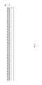
- FIG. 1 is a cross-sectional diagram a wearable power management system in accordance with an embodiment of the present patent application.
- FIG. 2 is a cross-sectional diagram of a circuit layer of the wearable power management system as depicted in FIG. 1 .
- FIG. 3 is a top view of the circuit layer as depicted in FIG. 2 .
- FIG. 4 is a cross-sectional diagram of a connection layer of the circuit layer as depicted in FIG. 2 .
- wearable power management system disclosed in the present patent application is not limited to the precise embodiments described below and that various changes and modifications thereof may be effected by one skilled in the art without departing from the spirit or scope of the protection.
- devices and/or features of different illustrative embodiments may be combined with each other and/or substituted for each other within the scope of this disclosure.
- FIG. 1 is a cross-sectional diagram of a wearable power management system in accordance with an embodiment of the present patent application.
- the wearable power management system includes a bottom coating layer 101 ; a bottom center layer 103 disposed above the bottom coating layer 101 ; a circuit layer 104 disposed above the bottom center layer 103 ; a top center layer 105 disposed above the circuit layer 104 ; and a top coating layer 107 disposed above top center layer 105 .
- the bottom center layer 103 and the top center layer 105 are made of an ultra-low Young's modulus material. In this embodiment, the Young's modulus of the material is in the range of 2.5 kPa-4.5 kPa.
- the thickness of both the bottom center layer and the top center layer is in the range of 250 um-350 um.
- Such configuration enables the circuit layer 104 to move freely in the bottom center 103 and the top center layer 105 so as to avoid being damaged under an external force, because the bottom center layer 103 and the top center layer 105 have relatively good elasticity and ductility.
- the Young's modulus of the bottom coating layer 101 and the top coating layer 107 is greater than the Young's modulus of the bottom center layer 103 and the top center layer 105 .
- the Young's modulus of both the bottom coating layer and the top coating layer is in the range of 50 kPa-70 kPa and the thickness of both the bottom coating layer and the top coating layer is in the range of 250 um-350 um.
- Such configuration makes the bottom coating layer 101 and the top coating layer 107 having a certain strength, so as to protect the bottom center layer 103 , the top center layer 105 and the circuit layer 104 , so that the wearable power management system can work properly in an environment where there are various types of external force.
- FIG. 2 is a cross-sectional diagram of the circuit layer 104 of the wearable power management system as depicted in FIG. 1 .
- the circuit layer 104 includes a device layer 201 ; and a connection layer 203 disposed above the device layer 203 .
- FIG. 3 is a top view of the circuit layer 104 as depicted in FIG. 2 .
- the device layer 201 includes a device matrix, which includes multiple solar cells and multiple rechargeable batteries.
- odd rows of the device matrix includes multiple solar cells 301
- even rows of the device matrix includes multiple rechargeable batteries 303 .
- the solar cells 301 are composite semiconductor solar cells with thickness between 30 um-40 um.
- the rechargeable batteries 303 are lithium-ion chip cells with thickness between 180 um-220 um.
- the device layer 201 further includes multiple alloy connection wires (not shown in FIG. 3 ).
- the alloy connection wires are connected and conducting between the device layer 201 and the connection layer 203 .
- the alloy connection wires are made of indium silver alloy, and therefore having relatively good conductivity and ductility.
- the device matrix structure as described above has a strong fault-tolerant capability. Even if one device is damaged and stops working properly, other devices of the system can continue to work, and therefore the stability of the wearable power management system is relatively high.
- connection layer 203 includes a connection wire network.
- the connection wire network includes multiple connection wires 305 and overlaps with the device matrix. Each device in the device matrix is connected to an adjacent device in the device matrix through the alloy connection wires and the connection wires 305 of the connection network.
- the connection wires essentially have a shape of sine waveforms, so as to maintain a certain flexible ductility. The shape of sine waveforms is similar to the antenna of insects. Such a bionic design can greatly relieve the impact that the connection wire 305 receives under an external force, and thereby further enhance the stability of the system.
- FIG. 4 is a cross-sectional diagram of the connection layer 203 of the circuit layer as depicted in FIG. 2 .
- the connection layer 203 includes a first polyimide layer 401 ; a copper layer 403 disposed above the first polyimide layer 401 ; and a second polyimide layer 405 disposed above copper product layer 403 . Because the density of the first polyimide layer 401 and the second polyimide layer 405 are relatively low, they are relatively light weight. In addition, they not only have relatively good elasticity and ductility, but also can provide a certain extent of strength. As a result, by their protection, the copper layer disposed between them can provide electrical connections continuously and stably under an external force.
- the solar cells 301 transform light energy into electrical energy when light is sufficient and charge the rechargeable batteries 303 , while the rechargeable batteries 303 are providing electric power to the wearable power management system.
- the circuit layer 104 can move freely in the bottom center 103 and the top center layer 105 , which have super low Young's modulus, so as to avoid being damaged, while at the same time obtaining a certain degree of protection provided by the bottom coating layer 101 and the top coating layer 107 , which have a relatively high Young's modulus.
- the device matrix structure as shown in FIG. 3 has a strong fault-tolerant capability. Even if one device is damaged and stops working properly, other devices of the system can continue to work, and therefore the stability of the wearable power management system is relatively high.
- connection wires 305 of the connection layer 205 essentially have a shape of sine waveforms, which is similar to the antenna of insects.
- Such a bionic design can greatly relieve the impact that the connection wire 305 receives under an external force, and thereby further enhance the stability of the system.
- the multilayer structure of the connection layer 203 as shown in FIG. 4 not only has light weight and relatively good elasticity and ductility, but also can provide a certain extent of strength, so that the copper layer disposed between the first polyimide layer 401 and the second polyimide layer 405 can provide electrical connections continuously and stably under an external force. Therefore, the wearable power management system provided in the above embodiment not only does not require any external power supply, therefore satisfying the requirements of the application over a wide range, but also is light, thin, soft, having good flexibility and work stability and long service life.
Landscapes
- Engineering & Computer Science (AREA)
- Chemical & Material Sciences (AREA)
- Electrochemistry (AREA)
- General Chemical & Material Sciences (AREA)
- Chemical Kinetics & Catalysis (AREA)
- Manufacturing & Machinery (AREA)
- Materials Engineering (AREA)
- Life Sciences & Earth Sciences (AREA)
- Sustainable Development (AREA)
- Sustainable Energy (AREA)
- Photovoltaic Devices (AREA)
- Electric Clocks (AREA)
- Power Engineering (AREA)
Abstract
Description
Claims (19)
Priority Applications (2)
| Application Number | Priority Date | Filing Date | Title |
|---|---|---|---|
| US15/603,450 US10483908B2 (en) | 2017-05-24 | 2017-05-24 | Wearable power management system |
| US16/654,033 US20200053867A1 (en) | 2017-05-24 | 2019-10-16 | Wearable power management system |
Applications Claiming Priority (1)
| Application Number | Priority Date | Filing Date | Title |
|---|---|---|---|
| US15/603,450 US10483908B2 (en) | 2017-05-24 | 2017-05-24 | Wearable power management system |
Related Child Applications (1)
| Application Number | Title | Priority Date | Filing Date |
|---|---|---|---|
| US16/654,033 Continuation-In-Part US20200053867A1 (en) | 2017-05-24 | 2019-10-16 | Wearable power management system |
Publications (2)
| Publication Number | Publication Date |
|---|---|
| US20170257060A1 US20170257060A1 (en) | 2017-09-07 |
| US10483908B2 true US10483908B2 (en) | 2019-11-19 |
Family
ID=59723801
Family Applications (1)
| Application Number | Title | Priority Date | Filing Date |
|---|---|---|---|
| US15/603,450 Expired - Fee Related US10483908B2 (en) | 2017-05-24 | 2017-05-24 | Wearable power management system |
Country Status (1)
| Country | Link |
|---|---|
| US (1) | US10483908B2 (en) |
Cited By (1)
| Publication number | Priority date | Publication date | Assignee | Title |
|---|---|---|---|---|
| CN109950351A (en) * | 2019-03-19 | 2019-06-28 | 天津三安光电有限公司 | A kind of bent flexible solar cell and preparation method thereof |
Families Citing this family (1)
| Publication number | Priority date | Publication date | Assignee | Title |
|---|---|---|---|---|
| WO2025073022A1 (en) * | 2023-10-02 | 2025-04-10 | Virgilio Silva Charles | Structural arrangement for a multi-layer photovoltaic module, composed of laminated cells and batteries, for use in panels and/or tiles |
Citations (9)
| Publication number | Priority date | Publication date | Assignee | Title |
|---|---|---|---|---|
| US20090072780A1 (en) * | 2007-09-13 | 2009-03-19 | Joong Kee Lee | Photovoltaic-Charged Secondary Battery System |
| US20100229923A1 (en) * | 2009-03-13 | 2010-09-16 | Sunlight Photonics Inc. | Stretchable photovoltaic devices and carriers |
| US20120300440A1 (en) * | 2010-01-28 | 2012-11-29 | Miyamae Ichiro | Solar battery power supply device |
| WO2013112883A1 (en) * | 2012-01-26 | 2013-08-01 | Dow Corning Corporation | Method of forming a photovoltaic cell module |
| US20140124014A1 (en) * | 2012-11-08 | 2014-05-08 | Cogenra Solar, Inc. | High efficiency configuration for solar cell string |
| US20140318602A1 (en) * | 2013-04-30 | 2014-10-30 | First Solar, Inc. | Integrated power connectors for pv modules and their methods of manufacture |
| US20140367644A1 (en) * | 2013-06-13 | 2014-12-18 | Samsung Display Co., Ltd. | Display apparatus having improved bending properties and method of manufacturing same |
| US20150287860A1 (en) * | 2014-04-07 | 2015-10-08 | Shin-Etsu Chemical Co., Ltd. | Solar cell encapsulant silicone composition and solar cell module |
| US20160218327A1 (en) * | 2015-01-22 | 2016-07-28 | Semiconductor Energy Laboratory Co., Ltd. | Secondary battery and electronic device |
Family Cites Families (1)
| Publication number | Priority date | Publication date | Assignee | Title |
|---|---|---|---|---|
| WO2008038232A2 (en) * | 2006-09-26 | 2008-04-03 | Discovery Holdings Limited | A system and method for rewarding employees of an organisation |
-
2017
- 2017-05-24 US US15/603,450 patent/US10483908B2/en not_active Expired - Fee Related
Patent Citations (9)
| Publication number | Priority date | Publication date | Assignee | Title |
|---|---|---|---|---|
| US20090072780A1 (en) * | 2007-09-13 | 2009-03-19 | Joong Kee Lee | Photovoltaic-Charged Secondary Battery System |
| US20100229923A1 (en) * | 2009-03-13 | 2010-09-16 | Sunlight Photonics Inc. | Stretchable photovoltaic devices and carriers |
| US20120300440A1 (en) * | 2010-01-28 | 2012-11-29 | Miyamae Ichiro | Solar battery power supply device |
| WO2013112883A1 (en) * | 2012-01-26 | 2013-08-01 | Dow Corning Corporation | Method of forming a photovoltaic cell module |
| US20140124014A1 (en) * | 2012-11-08 | 2014-05-08 | Cogenra Solar, Inc. | High efficiency configuration for solar cell string |
| US20140318602A1 (en) * | 2013-04-30 | 2014-10-30 | First Solar, Inc. | Integrated power connectors for pv modules and their methods of manufacture |
| US20140367644A1 (en) * | 2013-06-13 | 2014-12-18 | Samsung Display Co., Ltd. | Display apparatus having improved bending properties and method of manufacturing same |
| US20150287860A1 (en) * | 2014-04-07 | 2015-10-08 | Shin-Etsu Chemical Co., Ltd. | Solar cell encapsulant silicone composition and solar cell module |
| US20160218327A1 (en) * | 2015-01-22 | 2016-07-28 | Semiconductor Energy Laboratory Co., Ltd. | Secondary battery and electronic device |
Cited By (1)
| Publication number | Priority date | Publication date | Assignee | Title |
|---|---|---|---|---|
| CN109950351A (en) * | 2019-03-19 | 2019-06-28 | 天津三安光电有限公司 | A kind of bent flexible solar cell and preparation method thereof |
Also Published As
| Publication number | Publication date |
|---|---|
| US20170257060A1 (en) | 2017-09-07 |
Similar Documents
| Publication | Publication Date | Title |
|---|---|---|
| US10804597B2 (en) | Antenna system and communication terminal | |
| JP6172331B2 (en) | Manufacturing method of electronic equipment | |
| US9871295B2 (en) | Multi-scale, multi-layer diode grid array rectenna | |
| CN110212285B (en) | Near field communication antenna, manufacturing method thereof, display module and display system | |
| WO2015100762A1 (en) | Flexible wearable lithium battery | |
| US10396392B2 (en) | Electrochemical cell | |
| US20230238666A1 (en) | Electrochemical device and electronic device | |
| TW201249000A (en) | Antenna with multiple resonating conditions | |
| US20150145731A1 (en) | Electronic device | |
| US10483908B2 (en) | Wearable power management system | |
| CN104701472A (en) | Tensible and bendable flexible battery structure | |
| CN104282848A (en) | Flexible battery structure | |
| US20200053867A1 (en) | Wearable power management system | |
| GB2562736B (en) | Wearable power management system | |
| JP2021170853A (en) | Antenna and radio communication device | |
| CN105355851A (en) | Flexible electrode with slender holes and battery with electrode | |
| KR101767730B1 (en) | Wearable smart device having flexible semiconductor package on a band | |
| US20040224223A1 (en) | Battery in watchband | |
| CN108770162A (en) | An antistatic device and terminal equipment | |
| CN111149216B (en) | Wearable Power Management System | |
| CN108879101A (en) | Annular circular polarization implanted microstrip antenna | |
| CN102956991B (en) | Antenna | |
| Liang et al. | A printed dipole array antenna for non-contact monitoring system | |
| CN105204323B (en) | Waterproof health monitoring intelligent watch | |
| CN207474772U (en) | A kind of Miniature radio-frequency connector |
Legal Events
| Date | Code | Title | Description |
|---|---|---|---|
| AS | Assignment |
Owner name: MANQING TECHNOLOGY LIMITED, HONG KONG Free format text: ASSIGNMENT OF ASSIGNORS INTEREST;ASSIGNOR:KANG, MAN QING;REEL/FRAME:042484/0443 Effective date: 20170524 |
|
| AS | Assignment |
Owner name: SHENZHEN DANSHA TECHNOLOGY CO., LTD., CHINA Free format text: ASSIGNMENT OF ASSIGNORS INTEREST;ASSIGNOR:MANQING TECHNOLOGY LIMITED;REEL/FRAME:043026/0711 Effective date: 20170717 |
|
| STPP | Information on status: patent application and granting procedure in general |
Free format text: NON FINAL ACTION MAILED |
|
| STPP | Information on status: patent application and granting procedure in general |
Free format text: NOTICE OF ALLOWANCE MAILED -- APPLICATION RECEIVED IN OFFICE OF PUBLICATIONS |
|
| STCF | Information on status: patent grant |
Free format text: PATENTED CASE |
|
| FEPP | Fee payment procedure |
Free format text: MAINTENANCE FEE REMINDER MAILED (ORIGINAL EVENT CODE: REM.); ENTITY STATUS OF PATENT OWNER: MICROENTITY |
|
| LAPS | Lapse for failure to pay maintenance fees |
Free format text: PATENT EXPIRED FOR FAILURE TO PAY MAINTENANCE FEES (ORIGINAL EVENT CODE: EXP.); ENTITY STATUS OF PATENT OWNER: MICROENTITY |
|
| STCH | Information on status: patent discontinuation |
Free format text: PATENT EXPIRED DUE TO NONPAYMENT OF MAINTENANCE FEES UNDER 37 CFR 1.362 |
|
| FP | Lapsed due to failure to pay maintenance fee |
Effective date: 20231119 |