US10475979B2 - Thermoelectric materials, thermoelectric module including thermoelectric materials, and thermoelectric apparatus including thermoelectric modules - Google Patents
Thermoelectric materials, thermoelectric module including thermoelectric materials, and thermoelectric apparatus including thermoelectric modules Download PDFInfo
- Publication number
- US10475979B2 US10475979B2 US15/461,546 US201715461546A US10475979B2 US 10475979 B2 US10475979 B2 US 10475979B2 US 201715461546 A US201715461546 A US 201715461546A US 10475979 B2 US10475979 B2 US 10475979B2
- Authority
- US
- United States
- Prior art keywords
- thermoelectric
- thermoelectric material
- electrode
- group
- layer
- Prior art date
- Legal status (The legal status is an assumption and is not a legal conclusion. Google has not performed a legal analysis and makes no representation as to the accuracy of the status listed.)
- Active, expires
Links
Images


Classifications
-
- H01L35/28—
-
- C—CHEMISTRY; METALLURGY
- C01—INORGANIC CHEMISTRY
- C01B—NON-METALLIC ELEMENTS; COMPOUNDS THEREOF; METALLOIDS OR COMPOUNDS THEREOF NOT COVERED BY SUBCLASS C01C
- C01B19/00—Selenium; Tellurium; Compounds thereof
- C01B19/002—Compounds containing, besides selenium or tellurium, more than one other element, with -O- and -OH not being considered as anions
-
- C—CHEMISTRY; METALLURGY
- C01—INORGANIC CHEMISTRY
- C01G—COMPOUNDS CONTAINING METALS NOT COVERED BY SUBCLASSES C01D OR C01F
- C01G15/00—Compounds of gallium, indium or thallium
- C01G15/006—Compounds containing gallium, indium or thallium, with or without oxygen or hydrogen, and containing two or more other elements
-
- C—CHEMISTRY; METALLURGY
- C01—INORGANIC CHEMISTRY
- C01G—COMPOUNDS CONTAINING METALS NOT COVERED BY SUBCLASSES C01D OR C01F
- C01G17/00—Compounds of germanium
- C01G17/006—Compounds containing germanium, with or without oxygen or hydrogen, and containing two or more other elements
-
- C—CHEMISTRY; METALLURGY
- C01—INORGANIC CHEMISTRY
- C01G—COMPOUNDS CONTAINING METALS NOT COVERED BY SUBCLASSES C01D OR C01F
- C01G19/00—Compounds of tin
- C01G19/006—Compounds containing tin, with or without oxygen or hydrogen, and containing two or more other elements
-
- C—CHEMISTRY; METALLURGY
- C01—INORGANIC CHEMISTRY
- C01G—COMPOUNDS CONTAINING METALS NOT COVERED BY SUBCLASSES C01D OR C01F
- C01G28/00—Compounds of arsenic
- C01G28/002—Compounds containing arsenic, with or without oxygen or hydrogen, and containing two or more other elements
-
- C—CHEMISTRY; METALLURGY
- C01—INORGANIC CHEMISTRY
- C01G—COMPOUNDS CONTAINING METALS NOT COVERED BY SUBCLASSES C01D OR C01F
- C01G29/00—Compounds of bismuth
- C01G29/006—Compounds containing bismuth, with or without oxygen or hydrogen, and containing two or more other elements
-
- C—CHEMISTRY; METALLURGY
- C01—INORGANIC CHEMISTRY
- C01G—COMPOUNDS CONTAINING METALS NOT COVERED BY SUBCLASSES C01D OR C01F
- C01G3/00—Compounds of copper
-
- H01L35/16—
-
- H01L35/26—
-
- H—ELECTRICITY
- H10—SEMICONDUCTOR DEVICES; ELECTRIC SOLID-STATE DEVICES NOT OTHERWISE PROVIDED FOR
- H10N—ELECTRIC SOLID-STATE DEVICES NOT OTHERWISE PROVIDED FOR
- H10N10/00—Thermoelectric devices comprising a junction of dissimilar materials, i.e. devices exhibiting Seebeck or Peltier effects
- H10N10/10—Thermoelectric devices comprising a junction of dissimilar materials, i.e. devices exhibiting Seebeck or Peltier effects operating with only the Peltier or Seebeck effects
-
- H—ELECTRICITY
- H10—SEMICONDUCTOR DEVICES; ELECTRIC SOLID-STATE DEVICES NOT OTHERWISE PROVIDED FOR
- H10N—ELECTRIC SOLID-STATE DEVICES NOT OTHERWISE PROVIDED FOR
- H10N10/00—Thermoelectric devices comprising a junction of dissimilar materials, i.e. devices exhibiting Seebeck or Peltier effects
- H10N10/80—Constructional details
- H10N10/85—Thermoelectric active materials
- H10N10/851—Thermoelectric active materials comprising inorganic compositions
- H10N10/852—Thermoelectric active materials comprising inorganic compositions comprising tellurium, selenium or sulfur
-
- H—ELECTRICITY
- H10—SEMICONDUCTOR DEVICES; ELECTRIC SOLID-STATE DEVICES NOT OTHERWISE PROVIDED FOR
- H10N—ELECTRIC SOLID-STATE DEVICES NOT OTHERWISE PROVIDED FOR
- H10N10/00—Thermoelectric devices comprising a junction of dissimilar materials, i.e. devices exhibiting Seebeck or Peltier effects
- H10N10/80—Constructional details
- H10N10/85—Thermoelectric active materials
- H10N10/857—Thermoelectric active materials comprising compositions changing continuously or discontinuously inside the material
-
- C—CHEMISTRY; METALLURGY
- C01—INORGANIC CHEMISTRY
- C01P—INDEXING SCHEME RELATING TO STRUCTURAL AND PHYSICAL ASPECTS OF SOLID INORGANIC COMPOUNDS
- C01P2006/00—Physical properties of inorganic compounds
- C01P2006/32—Thermal properties
-
- C—CHEMISTRY; METALLURGY
- C01—INORGANIC CHEMISTRY
- C01P—INDEXING SCHEME RELATING TO STRUCTURAL AND PHYSICAL ASPECTS OF SOLID INORGANIC COMPOUNDS
- C01P2006/00—Physical properties of inorganic compounds
- C01P2006/40—Electric properties
-
- Y—GENERAL TAGGING OF NEW TECHNOLOGICAL DEVELOPMENTS; GENERAL TAGGING OF CROSS-SECTIONAL TECHNOLOGIES SPANNING OVER SEVERAL SECTIONS OF THE IPC; TECHNICAL SUBJECTS COVERED BY FORMER USPC CROSS-REFERENCE ART COLLECTIONS [XRACs] AND DIGESTS
- Y02—TECHNOLOGIES OR APPLICATIONS FOR MITIGATION OR ADAPTATION AGAINST CLIMATE CHANGE
- Y02P—CLIMATE CHANGE MITIGATION TECHNOLOGIES IN THE PRODUCTION OR PROCESSING OF GOODS
- Y02P20/00—Technologies relating to chemical industry
- Y02P20/10—Process efficiency
- Y02P20/129—Energy recovery, e.g. by cogeneration, H2recovery or pressure recovery turbines
-
- Y02P20/13—
Definitions
- thermoelectric materials having a high figure-of-merit thermoelectric modules including the thermoelectric materials, and thermoelectric apparatuses including the thermoelectric modules, and more particularly, to dichalcogenide thermoelectric materials having a high Seebeck coefficient, high electrical conductivity, and low thermal conductivity, thermoelectric modules including the thermoelectric materials, and thermoelectric apparatuses including the thermoelectric modules.
- Thermoelectric materials can be applied in active cooling and cogeneration using the Peltier effect and Seebeck effect.
- the Peltier effect refers to a phenomenon whereby, when an external DC voltage is applied as illustrated in FIG. 1 , holes in a p-type material and electrons in an n-type material are transported and thus one end of each of the respective materials absorbs heat and the other end of the materials releases heat.
- the Seebeck effect refers to a phenomenon whereby, when heat is supplied by an external heat source as illustrated in FIG. 2 , electrons and holes are transported and thus current flows in a material, thereby generating power.
- thermoelectric active cooling can improve the thermal stability of a device, does not generate vibration and noise, and does not use a separate condenser or refrigerant.
- thermoelectric active cooling is regarded as an environmentally friendly method of cooling that is suitable for small devices.
- Active cooling with thermoelectric materials can be applied in refrigerators or air conditioners that do not include refrigerants, and various other micro-cooling systems. Further, a uniform, stable temperature may be obtained. Accordingly, the performance of the device may be improved.
- waste heat may be used as an energy source. Accordingly, the energy efficiency of car engines or exhausts may be improved. Also, electrical power may be generated from waste incinerators or from the waste heat of ironworking. In addition, the efficiency of a power source for a medical device, which uses body heat and is installed inside the body, may be increased. Thus waste heat may be collected and used in various applications.
- thermoelectric material A factor for evaluating the performance of a thermoelectric material is a dimensionless figure-of-merit ZT that is defined by Equation 1:
- ZT S 2 ⁇ ⁇ T k Equation ⁇ ⁇ 1
- S is a Seebeck coefficient
- a electrical conductivity
- T is an absolute temperature
- k thermal conductivity
- thermoelectric materials having a high Seebeck coefficient, high electrical conductivity, and low thermal conductivity.
- thermoelectric modules including the thermoelectric materials.
- thermoelectric apparatuses including the thermoelectric modules.
- a thermoelectric material includes a dichalcogenide compound represented by Formula 1: R a T b X 2-n Y n (1) wherein R is a rare earth element, T includes at least one element selected from the group consisting of Group 1 elements, Group 2 elements, and a transition metal, X includes at least one element selected from the group consisting of S, Se, and Te, Y is different from X and includes at least one element selected from the group consisting of S, Se, Te, P, As, Sb, Bi, C, Si, Ge, Sn, B, Al, Ga and In, a is greater than 0 and less than or equal to 1, b is greater than or equal to 0 and less than 1, and n is greater than or equal to 0 and less than 2, wherein a+b is greater than 1 and less than or equal to 2.
- R is a rare earth element
- T includes at least one element selected from the group consisting of Group 1 elements, Group 2 elements, and a transition metal
- X includes at least one element selected from the group
- thermoelectric material may have a disordered structure in an in-plane direction, and may have the structure represented by Formula 1.
- the thermoelectric material having a layered structure may include: a first layer including X, or X and Y; and a second layer including X and R, or X and Y and R, wherein the first layer and the second layer are alternately arranged and T is doped or intercalated between the first layer and the second layer.
- thermoelectric material may exhibit a charge density wave.
- thermoelectric material may have two-dimensional electrical conductivity characteristics.
- thermoelectric material may include a bulk phase.
- thermoelectric material may be polycrystalline or single-crystalline.
- thermoelectric module includes a first electrode, a second electrode, and a dichalcogenide compound represented by Formula 1 interposed between the first electrode and the second electrode.
- thermoelectric apparatus includes the thermoelectric module and a heat source.
- thermoelectric material represented by Formula 1 including a layered structure having a disordered structure in an in-plane direction: R a T b X 2-n Y n (1) wherein R is a rare earth element, T includes at least one element selected from the group consisting of Group 1 elements, Group 2 elements, and a transition metal, X includes at least one element selected from the group consisting of S, Se, and Te, Y is different from X and includes at least one element selected from the group consisting of S, Se, Te, P, As, Sb, Bi, C, Si, Ge, Sn, B, Al, Ga and In, a is greater than 0 and less than or equal to 1, b is greater than or equal to 0 and less than 1, and n is greater than or equal to 0 and less than 2.
- thermoelectric device including: a first electrode; a second electrode; and a thermoelectric material interposed between the first electrode and the second electrode, the thermoelectric material includes a dichalcogenide compound represented by Formula 1: R a T b X 2-n Y n (1) wherein R is a rare earth element, T includes at least one element selected from the group consisting of Group 1 elements, Group 2 elements, and a transition metal, X includes at least one element selected from the group consisting of S, Se, and Te, Y is different from X and includes at least one element selected from the group consisting of S, Se, Te, P, As, Sb, Bi, C, Si, Ge, Sn, B, Al, Ga and In, a is greater than 0 and less than or equal to 1, b is greater than or equal to 0 and less than 1, and n is greater than or equal to 0 and less than 2.
- R is a rare earth element
- T includes at least one element selected from the group consisting of Group 1 elements, Group 2 elements, and a transition
- thermoelectric apparatus includes: a heat source; and a thermoelectric device, the thermoelectric device includes: a first electrode; a second electrode; and a thermoelectric material interposed between the first electrode and the second electrode, the thermoelectric material includes a dichalcogenide compound represented by Formula 1: R a T b X 2-n Y n (1) wherein R is a rare earth element, T includes at least one element selected from the group consisting of Group 1 elements, Group 2 elements, and a transition metal, X includes at least one element selected from the group consisting of S, Se, and Te, Y is different from X and includes at least one element selected from the group consisting of S, Se, Te, P, As, Sb, Bi, C, Si, Ge, Sn, B, Al, Ga and In, a is greater than 0 and less than or equal to 1, b is greater than or equal to 0 and less than 1, and n is greater than or equal to 0 and less than 2.
- R is a rare earth element
- T includes at least one element selected
- FIG. 1 is a schematic diagram illustrating an exemplary embodiment of a thermoelectric cooling system using the Peltier effect
- FIG. 2 is a schematic diagram illustrating an exemplary embodiment of a thermoelectric power generation system using the Seebeck effect
- FIG. 3 is a schematic diagram illustrating the structure of an exemplary embodiment of R a T b X 2-n Y n according to an embodiment
- FIG. 4 is a graph of a thermoelectric module according to an embodiment
- FIG. 5 is a graph illustrating thermal conductivity of Ce 0.9 Cu 0.1 Se 2 measured according to Experimental Example 1;
- FIG. 6 is a graph illustrating a Seebeck coefficient of Ce 0.9 Cu 0.1 Se 2 measured according to Experimental Example 2;
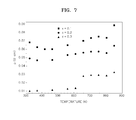
- FIG. 7 is a graph illustrating electrical resistance of Ce 0.9 Cu 0.1 Se 2 , Ce 0.8 Cu 0.2 Se 2 , and Ce 0.7 Cu 0.3 Se 2 measured according to Experimental Example 3;
- FIG. 8 is a graph illustrating a figure-of-merit of Ce 0.9 Cu 0.1 Se 2 calculated according to Experimental Example 4.
- the term “and/or” includes any and all combinations of one or more of the associated listed items. It will be understood that, although the terms first, second, third, etc., can be used herein to describe various elements, components, regions, layers and/or sections, these elements, components, regions, layers and/or sections should not be limited by these terms. These terms are only used to distinguish one element, component, region, layer or section from another region, layer or section. Thus, a first element, component, region, layer or section discussed below could be termed a second element, component, region, layer or section without departing from the teachings of the exemplary embodiments of the invention.
- spatially relative terms such as “below,” “lower,” “upper” and the like, can be used herein for ease of description to describe one element or feature's relationship to another element(s) or feature(s) as illustrated in the figures. It will be understood that the spatially relative terms are intended to encompass different orientations of the device in use or operation in addition to the orientation depicted in the figures. For example, if the device in the figures is turned over, elements described as “below” or “lower” relative to other elements or features would then be oriented “above” relative to the other elements or features. Thus, the exemplary term “below” can encompass both an orientation of above and below. The device can be otherwise oriented (rotated 90 degrees or at other orientations) and the spatially relative descriptors used herein interpreted accordingly.
- Embodiments of the invention are described herein with reference to illustrations that are schematic illustrations of idealized embodiments (and intermediate structures) of the invention. As such, variations from the shapes of the illustrations as a result, for example, of manufacturing techniques and/or tolerances, are to be expected. Thus, embodiments of the invention should not be construed as limited to the particular shapes of regions illustrated herein but are to include deviations in shapes that result, for example, from manufacturing. Thus, the regions illustrated in the figures are schematic in nature and their shapes are not intended to illustrate the actual shape of a region of a device and are not intended to limit the scope of the invention.
- thermoelectric materials may vary according to the structure thereof.
- a thermal conductivity (k tot ) of a material is the sum of a thermal conductivity (k Latt ) with respect to a lattice and a thermal conductivity (k el ) with respect to electrons.
- the thermal conductivity (k el ) with respect to electrons is determined according to the Wiedemann-Franz rule represented by Equation 2 below and thus, cannot be controlled. Accordingly, to reduce the thermal conductivity (k tot ) of the thermoelectric material, the thermal conductivity (k Latt ) with respect to the lattice may be decreased and the decrease may be achieved by controlling a lattice structure.
- thermoelectric material includes a dichalcogenide compound represented by Formula 1: R a T b X 2-n Y n where R is a rare earth element,
- T includes at least one element selected from the group consisting of Group 1 elements, Group 2 elements, and a transition metal
- X includes at least one element selected from the group consisting of S, Se, and Te,
- Y is different from X and includes at least one element selected from the group consisting of S, Se, Te, P, As, Sb, Bi, C, Si, Ge, Sn, B, Al, Ga and In,
- a is greater than 0 and less than or equal to 1,
- b is greater than or equal to 0 and less than 1,
- n is greater than or equal to 0 and less than 2.
- a+b may be greater than 1 and less than or equal to 2.
- the thermoelectric material may have a layered structure in which a first layer and a second layer are alternately disposed, wherein the first layer may include X, or X and Y, and the second layer may include X and R, or X and Y and R.
- first layer and the second layer elements are covalently bonded and irregularly arranged in an in-plane direction, and are thus strongly bonded to each other.
- first layer and the second layer may be bonded to each other by ionic bonding or van der Waals bonding, and are thus may be weakly bonded to each other in a c-axis direction.
- the thermoelectric material may have low thermal conductivity. Also, since electrons are transported through bonded elements, two-dimensional electrical conductivity characteristics may be obtained.
- thermoelectric material conductive electrons of X (S, Se, and Te: chalcogen) of the first layer may strongly interact with 4f orbital function electrons of R (rare earth element) of the second layer, and thus lattice distortion may occur and a charge density wave may be generated.
- T alkali metal, transition metal
- T alkali metal, transition metal
- the thermoelectric material may have high electrical conductivity and a high Seebeck coefficient.
- the intercalation of T may lead to an increase in the binding force in the c-axis direction, thereby enhancing mechanical strength of the thermoelectric material.
- the electrical conductivity and the Seebeck coefficient may also be increased by controlling the type or amount of Y.
- X may be partly substituted with Y in order to generate electrical conductivity in either electrons or holes, thereby controlling the current density of the thermoelectric material.
- thermoelectric material may be polycrystalline or single-crystalline. If the thermoelectric material is grown to be single-crystalline, a single crystal may be easily disposed in the c-axis direction in which thermal conductivity is low. Accordingly, the thermal conductivity may be further lowered and the figure-of-merit may be increased.
- thermoelectric material may have a bulk phase.
- thermoelectric material is polycrystalline
- the thermoelectric material may be prepared using one of the polycrystalline synthesis methods described below. However, the preparation method is not limited to these methods.
- thermoelectric material may be prepared by a method using ampoules, whereby a source material is loaded into a quartz tube, a metal ampoule or the like, and the tube or ampoule is sealed under vacuum, and then the sealed tube or ampoule is heat treated.
- thermoelectric material may be prepared by an arc melting method, whereby a source material is loaded into a chamber and then exposed to an arc discharge under an inactive gas atmosphere in order to melt the source material, thereby preparing a thermoelectric material.
- thermoelectric material may be prepared by a solid state reaction method, whereby a powder is mixed and the mixture is rigidly processed and heat treated, or the mixture is heat treated and then processed and sintered.
- thermoelectric material is single-crystalline
- the thermoelectric material may be prepared using one of the single crystal synthesis methods described below. However, the preparation method is not limited to these methods.
- a metal flux method whereby an element providing a condition under which a source material grows into a crystal at high temperature is loaded into a melting pot and then a heat treatment process is performed thereon at high temperature, thereby growing a crystal.
- a Bridgeman method whereby a source material is loaded into a melting pot and the source material at an end of the melting pot is heated at high temperature until the source material melts, and then, a high temperature zone is slowly shifted in order to locally melt the source material until the entire source material is completely exposed to the high temperature zone, thereby growing a crystal.
- a zone melting method whereby a source material is formed in a seed rod and a feed rod and a portion of the source material is melted by local heating at high temperature, and then the molten zone is slowly moved upward, thereby growing a crystal.
- a vapor transport method whereby a source material is placed at the bottom of a quartz tube and heated, and the top of the quartz tube has a low temperature, wherein, when the source material is evaporated, the evaporated source material is solidified, thereby growing a crystal.
- thermoelectric material may be manufactured using any of the methods described above, and the method is not limited thereto.
- thermoelectric material is polycrystalline
- a compression process may be additionally performed.
- electrical conductivity may be further improved.
- Examples of the compression process include hot pressing method, whereby a powder compound is loaded into a mold having a selected shape and then molding is performed at high temperature, for example, at a temperature of about 300 to about 800° C., and at high pressure, for example, at a pressure of about 30 to about 300 MPa;
- a spark plasma sintering method whereby a power compound is sintered for a short period of time by applying a high current, for example, a current of 50 to 500 A thereto at a high pressure, for example, a pressure of about 30 MPa to about 300 MPa; and a hot forging method, whereby during molding under pressure, a powder is subjected to extruding and sintering at high temperature, for example, at a temperature of about 300 to about 700° C.
- the density of the thermoelectric material reaches about 70 to about 100% of a theory density.
- the theory density is calculated by divining a molecular weight by an atomic volume, and evaluated as a lattice constant.
- the thermoelectric material has a density of about 95 to about 100% and thus has higher electrical conductivity.
- thermoelectric device is obtained by molding the thermoelectric material by, for example, cutting. If the thermoelectric material has a single-crystalline structure, the cutting direction of the thermoelectric material may be perpendicular to a growth direction.
- the thermoelectric device may be a p-type thermoelectric device or n-type thermoelectric device.
- the thermoelectric device is manufactured by forming the thermoelectric material into a selected shape, for example, into a rectangular parallelepiped.
- thermoelectric device may have a cooling effect when combined with an electrode and a current is applied thereto, and also have a power generation effect due to the device or a temperature difference.
- FIG. 4 is a view of a thermoelectric module including a thermoelectric device, according to an embodiment.
- a top electrode 12 and a bottom electrode 22 are patterned on a top insulating substrate 11 and a bottom insulating substrate 21 .
- the top electrode 12 and the bottom electrode 22 contact a p-type thermoelectric component 15 and an n-type thermoelectric component 16 .
- the top and bottom electrodes 12 and 22 are connected to the outside the thermoelectric device by a lead electrode 24 .
- the top and bottom insulating substrates 11 and 21 may be a gallium arsenic GaAs, sapphire, silicon, Firex, or quartz substrate.
- the top and bottom electrodes 12 and 22 may include aluminum, nickel, gold, or titanium, and may have various sizes.
- the top and bottom electrodes 12 and 22 may be formed using any conventional pattering method.
- the top and bottom electrodes 12 and 22 may be formed using a lift-off semiconductor process, a deposition method, or a photolithography technique.
- the thermoelectric module may include, as illustrated in FIGS. 1 and 2 , a first electrode, a second electrode, and the thermoelectric material represented by Formula 1 interposed between the first electrode and the second electrode.
- the thermoelectric module may further include, as illustrated in FIG. 4 , an insulating substrate on which at least one of the first electrode and the second electrode is disposed.
- the insulating substrate may be the insulating substrate that has been described above.
- thermoelectric module either the first electrode or the second electrode may be exposed to a heat source as illustrated in FIGS. 1 and 2 .
- thermoelectric device either the first electrode or the second electrode may be electrically connected to a power supplier illustrated in FIG. 1 , or to the outside the thermoelectric module, for example, an electric device (for example, battery) that consumes or stores electric powder.
- an electric device for example, battery
- thermoelectric module in the thermoelectric module, either the first electrode or the second electrode may be electrically connected to a power supplier illustrated in FIG. 1 .
- thermoelectric module in the thermoelectric module, as illustrated in FIG. 4 , the p-type thermoelectric device and the n-type thermoelectric device may be alternately disposed, and at least one of the p-type thermoelectric device and the n-type thermoelectric device may include the thermoelectric material containing the dichalcogenide compound represented by Formula 1.
- thermoelectric apparatus includes a heat source and the thermoelectric module, wherein the thermoelectric module includes a thermoelectric material that absorbs heat from the heat source and contains the dichalcogenide compound represented by Formula 1, a first electrode, and a second electrode, wherein the second electrode faces the first electrode. Either the first electrode or the second electrode may contact the thermoelectric material.
- thermoelectric apparatus may further include an electric power supplier that is electrically connected to the first electrode and the second electrode. According to another embodiment, the thermoelectric apparatus may further include an electric power supplier that is electrically connected to either the first electrode or the second electrode.
- thermoelectric material, the thermoelectric device, the thermoelectric module, and the thermoelectric apparatus may be, for example, a thermoelectric cooling system or a thermoelectric power generation system, and the thermoelectric cooling system may be a micro cooling system, a conventionally used cooling device, an air conditioner, or a waste heat power generation system, but is not limited thereto.
- thermoelectric cooling system may be a micro cooling system, a conventionally used cooling device, an air conditioner, or a waste heat power generation system, but is not limited thereto.
- the structure and manufacturing method of the thermoelectric cooling system are well known in the art and thus will not be described in detail herein.
- Ce, Se and Cu were quantified in molar ratios of 1:2.3:0.1, 1:2.3:0.2, and 1:2.3:0.3 and then each mixture was placed into an ampoule made of a quartz tube. Each of the ampoules was vacuum-sealed and heat treated at 850° C. for 24 hours, thereby synthesizing Ce 0.9 Cu 0.1 Se 2 , Ce 0.8 Cu 0.2 Se 2 , and Ce 0.7 Cu 0.3 Se 2 . In this case, the molar ratios of the respective compounds were identified by inductively coupled plasma spectroscopy.
- thermoelectric materials synthesized in Example 1 the thermal conductivity of Ce 0.9 Cu 0.1 Se 2 was measured. The results are shown in FIG. 5 .
- the thermal conductivity was evaluated based on thermal relaxation measured using a laser flash method.
- thermoelectric material was as low as about 1.2 W/mK at a temperature of 300 K. Such thermal conductivity is far lower than that of a commercially available thermoelectric material such as Bi 2 Te 3 , or Sb-doped Bi 2 Te 3 .
- thermoelectric material synthesized in Example 1 the Seebeck coefficient of Ce 0.9 Cu 0.1 Se 2 was measured. The results are shown in FIG. 6 .
- the Seebeck coefficient was as high as 320 to 350 ⁇ V/K in a thermoelectric material evaluation temperature region in a range of 300 to 800 K.
- the Seebeck coefficient was measured using a 4-terminal method.
- the electrical resistance of Ce 0.9 Cu 0.1 Se 2 , Ce 0.8 Cu 0.2 Se 2 , and Ce 0.7 Cu 0.3 Se 2 which were synthesized according to Example 1 was measured. The results are shown in FIG. 7 .
- the electrical resistance was measured using a 4-terminal method.
- thermoelectric materials have very low electrical resistance, and as the amount of Cu used is increased, the electrical resistance is reduced.
- the thermoelectric materials have very high electrical conductivity.
- thermoelectric material had a very high figure-of-merit of 0.18 at a temperature of 800 K. Also, as the temperature increased, the figure-of-merit was significantly increased.
- thermoelectric materials according to the one or more of the above embodiments have a high Seebeck coefficient, high electrical conductivity, and low thermal conductivity, and thus have a high figure-of-merit. Accordingly, the thermoelectric materials are useful for refrigerators that do not include refrigerants, air conditioners, waste heat power generation, thermoelectric nuclear power generation for the military, aviation, and space industries, and micro cooling systems.
Landscapes
- Chemical & Material Sciences (AREA)
- Organic Chemistry (AREA)
- Inorganic Chemistry (AREA)
- Powder Metallurgy (AREA)
Abstract
RaTbX2-nYn (1)
wherein R is a rare earth element, T includes at least one element selected from the group consisting of Group 1 elements, Group 2 elements, and a transition metal, X includes at least one element selected from the group consisting of S, Se, and Te, Y is different from X and includes at least one element selected from the group consisting of S, Se, Te, P, As, Sb, Bi, C, Si, Ge, Sn, B, Al, Ga and In, a is greater than 0 and less than or equal to 1, b is greater than or equal to 0 and less than 1, and n is greater than or equal to 0 and less than 2.
Description
where S is a Seebeck coefficient, a is electrical conductivity, T is an absolute temperature, and k is thermal conductivity.
RaTbX2-nYn (1)
wherein R is a rare earth element, T includes at least one element selected from the group consisting of Group 1 elements, Group 2 elements, and a transition metal, X includes at least one element selected from the group consisting of S, Se, and Te, Y is different from X and includes at least one element selected from the group consisting of S, Se, Te, P, As, Sb, Bi, C, Si, Ge, Sn, B, Al, Ga and In, a is greater than 0 and less than or equal to 1, b is greater than or equal to 0 and less than 1, and n is greater than or equal to 0 and less than 2, wherein a+b is greater than 1 and less than or equal to 2.
RaTbX2-nYn (1)
wherein R is a rare earth element, T includes at least one element selected from the group consisting of Group 1 elements, Group 2 elements, and a transition metal, X includes at least one element selected from the group consisting of S, Se, and Te, Y is different from X and includes at least one element selected from the group consisting of S, Se, Te, P, As, Sb, Bi, C, Si, Ge, Sn, B, Al, Ga and In, a is greater than 0 and less than or equal to 1, b is greater than or equal to 0 and less than 1, and n is greater than or equal to 0 and less than 2.
Ked=LT/ρ(L=2.44×10−8 ΩW/K2) Equation 2
RaTbX2-nYn
where R is a rare earth element,
Claims (11)
RaTbX2-nYn (1)
Priority Applications (1)
| Application Number | Priority Date | Filing Date | Title |
|---|---|---|---|
| US15/461,546 US10475979B2 (en) | 2009-01-06 | 2017-03-17 | Thermoelectric materials, thermoelectric module including thermoelectric materials, and thermoelectric apparatus including thermoelectric modules |
Applications Claiming Priority (6)
| Application Number | Priority Date | Filing Date | Title |
|---|---|---|---|
| KR10-2009-0000829 | 2009-01-06 | ||
| KR20090000829 | 2009-01-06 | ||
| KR1020090090224A KR101688529B1 (en) | 2009-01-06 | 2009-09-23 | Thermoelectric materials, and thermoelectric module and thermoelectric apparatus comprising same |
| KR10-2009-0090224 | 2009-09-23 | ||
| US12/683,151 US9653672B2 (en) | 2009-01-06 | 2010-01-06 | Thermoelectric materials, thermoelectric module including thermoelectric materials, and thermoelectric apparatus including thermoelectric modules |
| US15/461,546 US10475979B2 (en) | 2009-01-06 | 2017-03-17 | Thermoelectric materials, thermoelectric module including thermoelectric materials, and thermoelectric apparatus including thermoelectric modules |
Related Parent Applications (1)
| Application Number | Title | Priority Date | Filing Date |
|---|---|---|---|
| US12/683,151 Division US9653672B2 (en) | 2009-01-06 | 2010-01-06 | Thermoelectric materials, thermoelectric module including thermoelectric materials, and thermoelectric apparatus including thermoelectric modules |
Publications (2)
| Publication Number | Publication Date |
|---|---|
| US20170186931A1 US20170186931A1 (en) | 2017-06-29 |
| US10475979B2 true US10475979B2 (en) | 2019-11-12 |
Family
ID=42310922
Family Applications (2)
| Application Number | Title | Priority Date | Filing Date |
|---|---|---|---|
| US12/683,151 Expired - Fee Related US9653672B2 (en) | 2009-01-06 | 2010-01-06 | Thermoelectric materials, thermoelectric module including thermoelectric materials, and thermoelectric apparatus including thermoelectric modules |
| US15/461,546 Active 2030-05-27 US10475979B2 (en) | 2009-01-06 | 2017-03-17 | Thermoelectric materials, thermoelectric module including thermoelectric materials, and thermoelectric apparatus including thermoelectric modules |
Family Applications Before (1)
| Application Number | Title | Priority Date | Filing Date |
|---|---|---|---|
| US12/683,151 Expired - Fee Related US9653672B2 (en) | 2009-01-06 | 2010-01-06 | Thermoelectric materials, thermoelectric module including thermoelectric materials, and thermoelectric apparatus including thermoelectric modules |
Country Status (1)
| Country | Link |
|---|---|
| US (2) | US9653672B2 (en) |
Families Citing this family (7)
| Publication number | Priority date | Publication date | Assignee | Title |
|---|---|---|---|---|
| WO2016191606A1 (en) | 2015-05-26 | 2016-12-01 | Geordge Mason University | Mechanical and thermal electric generators |
| EA030605B1 (en) * | 2017-03-01 | 2018-08-31 | Республиканское Государственное Предприятие На Праве Хозяйственного Ведения "Евразийский Национальный Университет Им. Л.Н. Гумилева" Министерства Образования И Науки Республики Казахстан | NEW THERMOELECTRIC MATERIAL LiCuS |
| KR102122573B1 (en) * | 2017-03-09 | 2020-06-12 | 주식회사 엘지화학 | Compound semiconductors and their application |
| KR102121436B1 (en) | 2017-06-27 | 2020-06-10 | 주식회사 엘지화학 | Chalcogen-containing compound, its preparation method and thermoelectric element comprising the same |
| US11358864B2 (en) | 2017-06-30 | 2022-06-14 | Lg Chem, Ltd. | Chalcogen-containing compound, its preparation method and thermoelectric element comprising the same |
| KR102138937B1 (en) * | 2017-09-29 | 2020-07-28 | 주식회사 엘지화학 | Chalcogen-containing compound, its preparation method and thermoelectric element comprising the same |
| WO2019066580A2 (en) * | 2017-09-29 | 2019-04-04 | 주식회사 엘지화학 | Chalcogen compound, method for preparing same, and thermoelectric element comprising same |
Citations (16)
| Publication number | Priority date | Publication date | Assignee | Title |
|---|---|---|---|---|
| SU351276A1 (en) | С. С. Горелик, А. С. Охотин , Т. Турдалиев | METHOD OF MANUFACTURING THERMOELECTRIC DOMAIN | ||
| US3197410A (en) | 1961-08-28 | 1965-07-27 | Du Pont | Thermoelectric compositions of ta w-se |
| US3223640A (en) | 1963-09-13 | 1965-12-14 | Du Pont | Thermoelectric compositions and process for producing same |
| US3306857A (en) | 1962-03-28 | 1967-02-28 | Du Pont | Solid solution of w-v sc and thermoelectric element consisting of same |
| US3372997A (en) | 1966-12-22 | 1968-03-12 | Du Pont | Ternary copper, zinc, cadmium and manganese dichalcogenides having the pyrite-type crystal structure |
| US3519402A (en) | 1963-01-22 | 1970-07-07 | American Cyanamid Co | Semiconductors and devices employing the same |
| US5039626A (en) | 1988-10-04 | 1991-08-13 | University Of Tokyo | Method for heteroepitaxial growth of a two-dimensional material on a three-dimensional material |
| US5458865A (en) | 1992-04-06 | 1995-10-17 | The United States Of America As Represented By The Secretary Of The Navy | Electrical components formed of lanthanide chalcogenides and method of preparation |
| US5958358A (en) | 1992-07-08 | 1999-09-28 | Yeda Research And Development Co., Ltd. | Oriented polycrystalline thin films of transition metal chalcogenides |
| JP2002270907A (en) | 2001-03-06 | 2002-09-20 | Nec Corp | Thermoelectric conversion material and device using the same |
| US6469227B1 (en) | 1999-12-10 | 2002-10-22 | Lectec Corporation | Antipruritic patch |
| JP2004288841A (en) | 2003-03-20 | 2004-10-14 | Rikogaku Shinkokai | Oxychalcogenides and thermoelectric materials |
| US20070262408A1 (en) | 2004-03-19 | 2007-11-15 | Hidenori Takagi | Thermistor Device |
| EP1930960A1 (en) | 2006-12-04 | 2008-06-11 | Aarhus Universitet | Use of thermoelectric materials for low temperature thermoelectric purposes |
| US20090211619A1 (en) | 2008-02-26 | 2009-08-27 | Marlow Industries, Inc. | Thermoelectric Material and Device Incorporating Same |
| KR20090106320A (en) | 2008-04-04 | 2009-10-08 | 삼성전자주식회사 | Decalcogenide Thermoelectric Materials |
Family Cites Families (1)
| Publication number | Priority date | Publication date | Assignee | Title |
|---|---|---|---|---|
| CA1265922A (en) | 1984-07-27 | 1990-02-20 | Helmut Tributsch | Photoactive pyrite layer and process for making and using same |
-
2010
- 2010-01-06 US US12/683,151 patent/US9653672B2/en not_active Expired - Fee Related
-
2017
- 2017-03-17 US US15/461,546 patent/US10475979B2/en active Active
Patent Citations (17)
| Publication number | Priority date | Publication date | Assignee | Title |
|---|---|---|---|---|
| SU351276A1 (en) | С. С. Горелик, А. С. Охотин , Т. Турдалиев | METHOD OF MANUFACTURING THERMOELECTRIC DOMAIN | ||
| US3197410A (en) | 1961-08-28 | 1965-07-27 | Du Pont | Thermoelectric compositions of ta w-se |
| US3306857A (en) | 1962-03-28 | 1967-02-28 | Du Pont | Solid solution of w-v sc and thermoelectric element consisting of same |
| US3519402A (en) | 1963-01-22 | 1970-07-07 | American Cyanamid Co | Semiconductors and devices employing the same |
| US3223640A (en) | 1963-09-13 | 1965-12-14 | Du Pont | Thermoelectric compositions and process for producing same |
| US3372997A (en) | 1966-12-22 | 1968-03-12 | Du Pont | Ternary copper, zinc, cadmium and manganese dichalcogenides having the pyrite-type crystal structure |
| US5039626A (en) | 1988-10-04 | 1991-08-13 | University Of Tokyo | Method for heteroepitaxial growth of a two-dimensional material on a three-dimensional material |
| US5458865A (en) | 1992-04-06 | 1995-10-17 | The United States Of America As Represented By The Secretary Of The Navy | Electrical components formed of lanthanide chalcogenides and method of preparation |
| US5958358A (en) | 1992-07-08 | 1999-09-28 | Yeda Research And Development Co., Ltd. | Oriented polycrystalline thin films of transition metal chalcogenides |
| US6469227B1 (en) | 1999-12-10 | 2002-10-22 | Lectec Corporation | Antipruritic patch |
| JP2002270907A (en) | 2001-03-06 | 2002-09-20 | Nec Corp | Thermoelectric conversion material and device using the same |
| US20030056819A1 (en) | 2001-03-06 | 2003-03-27 | Nec Corporation | Thermoelectric material and thermoelectric converting element using the same |
| JP2004288841A (en) | 2003-03-20 | 2004-10-14 | Rikogaku Shinkokai | Oxychalcogenides and thermoelectric materials |
| US20070262408A1 (en) | 2004-03-19 | 2007-11-15 | Hidenori Takagi | Thermistor Device |
| EP1930960A1 (en) | 2006-12-04 | 2008-06-11 | Aarhus Universitet | Use of thermoelectric materials for low temperature thermoelectric purposes |
| US20090211619A1 (en) | 2008-02-26 | 2009-08-27 | Marlow Industries, Inc. | Thermoelectric Material and Device Incorporating Same |
| KR20090106320A (en) | 2008-04-04 | 2009-10-08 | 삼성전자주식회사 | Decalcogenide Thermoelectric Materials |
Non-Patent Citations (13)
| Title |
|---|
| "Thermoelectric power generator", Encyclopedia Britannica Online Academic Edition, Encyclopaedia Britannica Inc, 2013. Web Sep. 18, 2013 <http://www.britannica.comEBchecked/topic/591615/therniekectruc-oier-generator>. |
| Aitken et al., "Metamagnetic Transition in EuSe2: A New, Metastable Binary Rare-Earth Polychalcogenide", Chem. Mater. vol. 10, 1998, pp. 3928-3935. |
| Bentien et al "Experimental and theoretical investigations of strongly correlated FeSb2-xSnx", Phys. Rev. B, 74, 205105, 2006. |
| Chiritescu, C. et al., "Ultralow Thermal Conductivity in Disordered, Layered WSe2 Crystals", Science, Jan. 2007, 315: 351-353. |
| Dung et al., "Single-Crystal Structure of Copper Lanthanum Telluride Cu0.28LaTe2: A Disordered Tunnel Structure", Acta Cryst., C39, 1983, pp. 668-670. |
| Gulay et al.., "Crystal structures of the compounds R3CuSiS7 (R=Ce, Pr, Nd, Sm, Tb, Dy and Er) and R3CuSiSe7 (R=La, Ce, Pr, Nd, Sm, Gd, Tb and Dy)", Journal of Alloys and Compounds, vol. 431, 2007, pp. 185-190. |
| Imai, H. et al., "Large thermoelectric power factor in TiS2 crystal with nearly stoichiometric composition", Phys. Rev. B (2001); 64, pp. 241104-1-4. |
| Internet Archive Wayback Machine of thermoelectric power generator article from Encyclopaedia Britannica, accessed Sep. 19, 2013 <http://web.archive.org/web/200805252094500://www.britannica.com/EBchecked/topic/591615/thermoelectric-power-generator>. |
| Qin, X. Y. et al., "The effect of Mg substitution for Ti on transport and thermoelectric properties of TiS2", J. of Applied Physics, vol. 102, Issue 7, pp. 073703-073703-7 (2007). |
| Reid et al., "Electrical Properties of Selected Rare Earth Compounds and Alloys", Journal of the Electrochemical Society, vol. 111, No. 8, Aug. 1964, pp. 943-950. |
| Sams et al., "Doping Studies and Thermoelectric Properties of TiS2", International Conference on Thermoelectrics, 2005, pp. 99-101. |
| Takeshita et al., "Preparation and Thermoelectric Properties of Some Rare Earth chalcogenides", The Rare Earths in Modern Science and Technology, vol. 3,1982, 255-256. |
| Wang et al., "Sulfur SToichiometry Effects in highly spin polarized CoS2 single crystals", App. Phys. Lett, 88, 232509-1-3, Jun. 2006. |
Also Published As
| Publication number | Publication date |
|---|---|
| US20100170553A1 (en) | 2010-07-08 |
| US9653672B2 (en) | 2017-05-16 |
| US20170186931A1 (en) | 2017-06-29 |
Similar Documents
| Publication | Publication Date | Title |
|---|---|---|
| US10475979B2 (en) | Thermoelectric materials, thermoelectric module including thermoelectric materials, and thermoelectric apparatus including thermoelectric modules | |
| US8933318B2 (en) | Thermoelectric material, and thermoelectric module and thermoelectric device including the thermoelectric material | |
| KR101688528B1 (en) | Thermoelectric materials, and thermoelectric module and thermoelectric device comprising same | |
| US8299349B2 (en) | Thermoelectric materials and chalcogenide compounds | |
| US8518287B2 (en) | Dichalcogenide thermoelectric material | |
| JP6401436B2 (en) | Thermoelectric material having strained electronic density of state, manufacturing method thereof, thermoelectric module and thermoelectric device including the same | |
| US9130066B2 (en) | Power factor enhanced thermoelectric material and method of producing same | |
| US9093597B2 (en) | Thermoelectric material, and thermoelectric module and thermoelectric device comprising the thermoelectric material | |
| US10600947B2 (en) | Thermoelectric materials, and thermoelectric element and thermoelectric module comprising the same | |
| KR20140116668A (en) | Natural superlattice structured thermoelectric materials | |
| US20140174494A1 (en) | Thermoelectric material, thermoelectric element and apparatus including the same, and preparation method thereof | |
| KR101688529B1 (en) | Thermoelectric materials, and thermoelectric module and thermoelectric apparatus comprising same | |
| US8986566B2 (en) | Thermoelectric material, thermoelectric device using the same, and method of manufacturing thereof |
Legal Events
| Date | Code | Title | Description |
|---|---|---|---|
| STPP | Information on status: patent application and granting procedure in general |
Free format text: NON FINAL ACTION MAILED |
|
| STPP | Information on status: patent application and granting procedure in general |
Free format text: RESPONSE TO NON-FINAL OFFICE ACTION ENTERED AND FORWARDED TO EXAMINER |
|
| STPP | Information on status: patent application and granting procedure in general |
Free format text: NOTICE OF ALLOWANCE MAILED -- APPLICATION RECEIVED IN OFFICE OF PUBLICATIONS |
|
| STPP | Information on status: patent application and granting procedure in general |
Free format text: PUBLICATIONS -- ISSUE FEE PAYMENT VERIFIED |
|
| STCF | Information on status: patent grant |
Free format text: PATENTED CASE |
|
| MAFP | Maintenance fee payment |
Free format text: PAYMENT OF MAINTENANCE FEE, 4TH YEAR, LARGE ENTITY (ORIGINAL EVENT CODE: M1551); ENTITY STATUS OF PATENT OWNER: LARGE ENTITY Year of fee payment: 4 |