US10468906B2 - Optical charging system with integrated sensor and power receiver - Google Patents
Optical charging system with integrated sensor and power receiver Download PDFInfo
- Publication number
- US10468906B2 US10468906B2 US15/415,055 US201715415055A US10468906B2 US 10468906 B2 US10468906 B2 US 10468906B2 US 201715415055 A US201715415055 A US 201715415055A US 10468906 B2 US10468906 B2 US 10468906B2
- Authority
- US
- United States
- Prior art keywords
- optical
- electronic device
- electrical signal
- photodiode
- led
- Prior art date
- Legal status (The legal status is an assumption and is not a legal conclusion. Google has not performed a legal analysis and makes no representation as to the accuracy of the status listed.)
- Active, expires
Links
Images


Classifications
-
- H02J7/355—
-
- H—ELECTRICITY
- H02—GENERATION; CONVERSION OR DISTRIBUTION OF ELECTRIC POWER
- H02J—CIRCUIT ARRANGEMENTS OR SYSTEMS FOR SUPPLYING OR DISTRIBUTING ELECTRIC POWER; SYSTEMS FOR STORING ELECTRIC ENERGY
- H02J50/00—Circuit arrangements or systems for wireless supply or distribution of electric power
- H02J50/30—Circuit arrangements or systems for wireless supply or distribution of electric power using light, e.g. lasers
-
- H—ELECTRICITY
- H02—GENERATION; CONVERSION OR DISTRIBUTION OF ELECTRIC POWER
- H02J—CIRCUIT ARRANGEMENTS OR SYSTEMS FOR SUPPLYING OR DISTRIBUTING ELECTRIC POWER; SYSTEMS FOR STORING ELECTRIC ENERGY
- H02J50/00—Circuit arrangements or systems for wireless supply or distribution of electric power
- H02J50/80—Circuit arrangements or systems for wireless supply or distribution of electric power involving the exchange of data, concerning supply or distribution of electric power, between transmitting devices and receiving devices
-
- H—ELECTRICITY
- H02—GENERATION; CONVERSION OR DISTRIBUTION OF ELECTRIC POWER
- H02J—CIRCUIT ARRANGEMENTS OR SYSTEMS FOR SUPPLYING OR DISTRIBUTING ELECTRIC POWER; SYSTEMS FOR STORING ELECTRIC ENERGY
- H02J7/00—Circuit arrangements for charging or depolarising batteries or for supplying loads from batteries
- H02J7/00032—Circuit arrangements for charging or depolarising batteries or for supplying loads from batteries characterised by data exchange
- H02J7/00034—Charger exchanging data with an electronic device, i.e. telephone, whose internal battery is under charge
-
- H02J7/0052—
-
- H—ELECTRICITY
- H02—GENERATION; CONVERSION OR DISTRIBUTION OF ELECTRIC POWER
- H02J—CIRCUIT ARRANGEMENTS OR SYSTEMS FOR SUPPLYING OR DISTRIBUTING ELECTRIC POWER; SYSTEMS FOR STORING ELECTRIC ENERGY
- H02J7/00—Circuit arrangements for charging or depolarising batteries or for supplying loads from batteries
- H02J7/007—Regulation of charging or discharging current or voltage
-
- H—ELECTRICITY
- H02—GENERATION; CONVERSION OR DISTRIBUTION OF ELECTRIC POWER
- H02J—CIRCUIT ARRANGEMENTS OR SYSTEMS FOR SUPPLYING OR DISTRIBUTING ELECTRIC POWER; SYSTEMS FOR STORING ELECTRIC ENERGY
- H02J7/00—Circuit arrangements for charging or depolarising batteries or for supplying loads from batteries
- H02J7/34—Parallel operation in networks using both storage and other dc sources, e.g. providing buffering
- H02J7/35—Parallel operation in networks using both storage and other dc sources, e.g. providing buffering with light sensitive cells
-
- H02J2007/0059—
-
- H02J2007/0062—
-
- H—ELECTRICITY
- H02—GENERATION; CONVERSION OR DISTRIBUTION OF ELECTRIC POWER
- H02J—CIRCUIT ARRANGEMENTS OR SYSTEMS FOR SUPPLYING OR DISTRIBUTING ELECTRIC POWER; SYSTEMS FOR STORING ELECTRIC ENERGY
- H02J2207/00—Indexing scheme relating to details of circuit arrangements for charging or depolarising batteries or for supplying loads from batteries
- H02J2207/20—Charging or discharging characterised by the power electronics converter
Definitions
- the disclosure relates generally to the field of wireless charging of electronic devices. More specifically, the disclosure relates to an optical charging system.
- Embodiments of the disclosure can provide an optical charging system with an integrated sensor and power receiver.
- An electronic device e.g., a wearable
- An electronic device can include an optical sensor for performing photometric measurements.
- a photodiode of the sensor can be shared and used for generating an electrical signal when exposed to a light source (e.g., LED) of a light power transmitter.
- the electrical signal can be conditioned by a power management circuit and can be used to charge a device battery.
- the light power transmitter can include a photodiode, which can be used for establishing a connection with the device using an optical signal emitted by a light source of the optical sensor.
- the light power transmitter can be power by, e.g., a USB connection.
- the intensity of the power transmitter light source can be regulated via a feedback signal from the device, based on the battery charging status.
- a method for optical charging of an electronic device can include detecting a current charge level of a battery of the electronic device.
- a feedback signal can be generated based on the current charge level of the battery.
- the feedback signal can be communicated to an optical charger via an optical transmitter of the electronic device.
- a light signal can be received from the optical charger. Intensity of the light signal can be based on the feedback signal.
- the light signal can be converted to an electrical signal.
- the battery can be charged using the electric signal.
- At least one computer-readable storage medium can be provided to include instructions that, when executed on a central processing unit (CPU) of an embedded sensor system, cause the CPU to . . . .
- FIG. 1 depicts an optical charging system with integrated sensor and power receiver, in accordance with an example embodiment.
- FIG. 2 depicts an example wearable device with an optical charging system, in accordance with an example embodiment.
- FIG. 3A depicts an example optical charging system with shared use of a sensor photodiode, in accordance with an example embodiment.
- FIG. 3B depicts an example optical charging system configured to establish a link between a power receiver and a power transmitter via optical communications, in accordance with an example embodiment.
- FIG. 4 illustrates a flow diagram of a method for optical charging of an electronic device, in accordance with an example embodiment.
- an electronic device can include an integrated sensor (e.g., for performing photometric measurements, such as heart rate measurement of a user), which can be shared with a power receiver for optical charging of the device. More specifically, light received from a light power transmitter can be converted to an electrical signal using a photovoltaic cell or a photodiode of the integrated sensor. The electrical signal can be further conditioned (e.g., voltage regulation and impedance matching) and then used for charging a battery of the electronic device.
- a light source within the integrated sensor e.g., a light emitting diode, or LED
- the light power transmitter can include a light source (e.g., LED) and a photodiode (or photovoltaic cell), and can be powered via a separate power source (e.g., via a uniform serial bus (USB) connection).
- the optical communication link between the power receiver and the power transmitter can be further used for communicating battery charge status signals so that the intensity of the light generated by the light power transmitter can be adjusted to control the battery charge.
- device charging can be performed while maintaining a sealed and waterproof device housing and while sharing an existing device sensor system. Additionally, the optical charging system discussed herein is space-efficient as it does not use an inductive coil, and device charging can still take place with a wider tolerance to placement position of the light transmitter in relation to the device.
- FIG. 1 depicts an optical charging system with integrated sensor and power receiver, in accordance with an example embodiment.
- an optical charging system 100 including a power transmitter 102 and a power receiver 104 .
- the power transmitter 102 may comprise suitable circuitry, logic, interfaces and/or code and can be configured for optical communication with the power receiver 104 to provide optical (light) signals for charging the battery (e.g., 130 ) of the power receiver, or to receive feedback signals indicative of the battery charge status.
- the power transmitter can include a power control block 108 , an LED driver block 110 , and an optical data receiver block 112 .
- the power transmitter 102 can further include a light source 114 , such as an LED, and a photodiode (or a photovoltaic cell) 116 .
- the power control block 108 may comprise suitable circuitry, logic, interfaces and/or code, and can be configured to limit amount of current drawn from power port 106 .
- the power port 106 can be a USB port configured to supply power in connection with one or more USB-related protocols, such as USB 1.0, USB 2.0, USB 3.0, or another type of connection protocol.
- the LED driver block 110 may comprise suitable circuitry, logic, interfaces and/or code, and can be configured to adjust current and/or voltage supplied to the LED 114 so as to adjust the transmitted light power density.
- the optical data receiver 112 may comprise suitable circuitry, logic, interfaces and/or code, and can be configured to communicate with the power receiver 104 via the photodiode 116 (e.g., receive feedback information regarding battery status) to activate or deactivate optical charging via the LED 114 , or adjust the transmitted light power density using the LED driver block 110 .
- the optical receiver 112 can include one or more analog-to-digital converters (ADCs), which can be used to monitor voltage signals generated by the photodiode 116 , and generate one or more control signals based on the voltage signals.
- the control signals can be communicated to the LED driver block 110 for, e.g., adjusting voltage and/or current supplied to the LED 114 .
- ADCs analog-to-digital converters
- the power receiver 104 can include a power management block 120 and a photometric front end block 128 .
- the photometric front end 128 can also include a photodiode 132 and an LED 134 .
- the photometric front end 128 and the power management block 120 can be implemented within a battery-powered electronic device with sensor capabilities (e.g., as illustrated in FIG. 2 ).
- the photometric front end 128 can be configured to perform photometric measurements using the LED 134 and the photodiode 132 .
- the photometric measurements can include photoplethysmography measurement to determine a heart rate of a user wearing the electronic device.
- Other types of measurements may be performed by the photometric front end as well, using the LED 134 and the photodiode 132 .
- Other light sources may be used in place of the LED 134 .
- a photovoltaic cell can be used in lieu of the photodiode 132 .
- the photometric front end 128 can also include an optical transmitter (e.g., as illustrated in FIG. 3A , FIG. 3B or FIG. 3C ).
- the optical transmitter may comprise suitable circuitry, logic, interfaces and/or code, and can be configured to generate one or more optical feedback signals for transmission to the power transmitter 102 via the LED 134 .
- the optical transmitter can include one or more digital-to-analog converters (DACs), which can be used to generate the feedback signals (e.g., as explained in greater detail herein below, in reference to FIG. 3B and FIG. 3C ).
- the optical transmitter may be part of the photometric front end 128 or the power management block 120 .
- the impedance matching block 124 may comprise suitable circuitry, logic, interfaces and/or code, and can be configured to perform impedance matching by regulating the voltage of the electrical signal generated by the photodiode 132 to a highest power extracting point so as to capture a maximum amount of energy emitted by the LED 114 .
- the charge management block 126 may comprise suitable circuitry, logic, interfaces and/or code, and can be configured to control charging the battery 130 using the conditioned and impedance matched electrical signal received from the impedance matching block 124 .
- the charge management block 126 can monitor the charge status of the battery 130 to prevent overcharge or over-discharge. In instances when the battery charge status indicates a charge above a first pre-determined threshold, a first control signal may be generated by the charge management block 126 and communicated via the LED 134 of the photometric front end 128 (or the optical transmitter, as illustrated in FIG. 3C ) to the power transmitter 102 to stop illumination by the LED 114 .
- a second control signal may be generated by the charge management block 126 and communicated via the LED 134 of the photometric front end 128 (or the optical transmitter, as illustrated in FIG. 3C ) to the power transmitter 102 to initiate charging by turning the LED 114 ON, or by adjusting the light intensity of the LED 114 .
- the charge management block 126 may also detect one or more operating conditions (e.g., operating temperature variance of the receiver 104 or alignment variance) and generate a control signal for adjusting the intensity of the LED 114 .
- FIG. 2 depicts an example wearable device with an optical charging system, in accordance with an example embodiment.
- the optical charging system 200 can include an electronic device 220 and a light power transmitter (or charger) 208 .
- the electronic device 220 can be a wearable device, such as a smart watch.
- the device 220 can include a power receiver 204 , which can be similar to the power receiver 104 .
- the charger 208 can include a power transmitter 202 , which can be similar to the power transmitter 102 .
- the device 220 can include LEDs 224 and photodiodes 222 , which can be part of a photometric front end (such as photometric front end 128 ) configured to perform photometric measurements.
- the photometric measurements can include photoplethysmography measurement to determine a heart rate of a user wearing the electronic device 220 .
- the photoplethysmography measurement can be performed by illuminating the user's skin (when the user is wearing the device 220 ) by the LEDs 224 , and generating an electric signal using the photodiodes 222 based on a reflection of the light from the LEDs 224 by the user's skin.
- the generated electric signal can be used to detect and measure the user's heart rate.
- the charger 208 can include a power connector 206 (e.g., a USB power connector), powering LED 210 .
- the charger 208 may further include a photodiode 212 .
- power delivery can be achieved when the LED 210 of charger 208 is illuminated and is placed in proximity to the photodiodes 222 of the device 220 .
- the photodiodes 222 can be shared for performing photometric functions or generating electrical signals for charging a device battery when the photodiodes 222 are illuminated by the LED 210 .
- one or more data communication paths may be established between the charger 208 and the device 220 .
- a data communication path from the charger 208 to the device 220 can be established using the LED 210 of the charger and the photodiodes 222 of the device 220 .
- Another data communication path from the device 220 to the charger 208 can be established using the LEDs 224 of the device 220 and the photodiode 212 of the charger 208 .
- the data communication paths can be used for, e.g., establishing an initial communication (such as a wireless “handshake”) as well as to communicate control signals for initiating battery charging or adjusting LED light intensity (for LED 210 ) based on charge status of a device 220 battery.
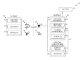
- FIG. 3A depicts an example optical charging system with shared use of a sensor photodiode, in accordance with an example embodiment.
- the optical charging system 300 can include a power transmitter (or transmit power management integrated circuit, “Tx PMIC”) 302 and a power receiver 304 .
- the power transmitter 302 can include similar components and perform similar functionalities as the power transmitter 102 of FIG. 1 .
- the power receiver 304 can include similar components and perform similar functionalities as the power receiver 104 of FIG. 1 .
- the power transmitter 302 can include a power control block 322 , an LED driver block 324 and an optical receiver block 326 , which can have functionalities that are similar to the functionalities performed by the power control block 108 , the LED driver block 110 , and the optical receiver block 112 , respectively.
- the power transmitter may also include an LED 328 and a photodiode (or a photovoltaic cell) 330 .
- the power receiver 304 can include a receiver power management integrated circuit (Rx PMIC) 306 and an optical sensor front end 308 , which can have functionalities that are similar to the functionalities performed by the power management block 120 and the photometric front end 128 , respectively.
- the Rx PMIC 306 can include a voltage regulator block 310 , an impedance matching block 312 , and a charge management block 314 , which can have functionalities that are similar to the functionalities performed by the voltage regulation block 122 , the impedance matching block 124 , and the charge management block 126 , respectively.
- the Rx PMIC 306 can also include an optical transmitter 316 .
- the optical transmitter 316 may comprise suitable circuitry, logic, interfaces and/or code, and can be configured to generate one or more optical signals for transmission to the Tx PMIC 302 via the LED 321 .
- the optical transmitter 316 can include one or more digital-to-analog converters (DACs), which can be used to generate the optical signals.
- DACs digital-to-analog converters
- the optical sensor 308 can include a current sensor block 318 , an LED driver block 320 , a photodiode (or photovoltaic cell) 319 , and an LED 321 .
- the current sensor block 318 may comprise suitable circuitry, logic, interfaces and/or code, and can be configured to sense an electric signal generated by the photodiode 319 .
- the LED driver block 320 may comprise suitable circuitry, logic, interfaces and/or code, and can be configured to adjust current and/or voltage supplied to the LED 321 so as to adjust the transmitted light power density.
- the photodiode 319 of the optical sensor 308 can be used for photometric sensing (e.g., in connection with LED 321 ) or for charging the battery 352 .
- the Tx PMIC 302 can activate the LED 328 , which can be placed in proximity to the photodiode 319 of the power receiver 304 .
- the photodiode 319 can generate an electric signal, which is sensed by the current sensor 318 of the optical sensor front end 308 .
- the electrical signal can be communicated via communication path 332 to the Rx PMIC 306 for further processing (e.g., by the voltage regulator block 310 or the impedance matching block 312 ).
- the charge management block may then use the processed/conditioned electrical signal to charge the battery 352 up to a pre-determined threshold level.
- photometric sensing without charging may be performed by the optical charging system 300 .
- FIG. 3B depicts an example optical charging system configured to establish a link between a power receiver and a power transmitter via optical communications, in accordance with an example embodiment.
- the optical charging system 100 can be configured to use an optical communication link between the Tx PMIC 302 and the power receiver 304 .
- the optical transmitter 316 can use the LED 321 to communicate one or more optical signals to the photodiode 330 in the Tx PMIC 302 via the communication link 342 .
- Communication link 342 may be bi-directional, with the Tx PMIC 302 communicating signals to the Rx PMIC 306 using the LED 328 and the photodiode 319 .
- Example optical signals may include “handshake” signals for establishing an initial communication between the Tx PMIC 302 and the power receiver 304 .
- Other example optical signals may include charging protocol signals associated with a charging protocol used by the Rx PMIC 306 for charging the battery 352 .
- FIG. 3C depicts an example optical charging system with feedback control using optical communications, in accordance with an example embodiment.
- the optical charging system 300 can be configured to use an optical data communication link between the Tx PMIC 302 and the Rx PMIC 306 for power management and control.
- the charge management block 314 can be configured to obtain charge status information 354 indicative of charge status of the battery 352 .
- the charge status information 354 can be communicated to the Tx PMIC 302 via the communication link 356 , established between the LED 321 and the photodiode 330 .
- the optical receiver 326 can receive the charge status information 354 , and can generate a control signal 358 based on the charge status information 354 .
- the control signal 358 can be used by the LED driver block 324 to turn the LED 328 ON, OFF, or adjust the intensity of the LED 328 based on the charge status information 354 .
- the charge status information 354 can indicate that the battery 352 is charged below a threshold amount.
- the control signal 358 can then be used to activate the LED 328 or increase the intensity of the LED 328 .
- the charge status information 354 can indicate that the battery 352 is charged above a threshold amount.
- the control signal 358 can then be used to decrease the intensity of the charging LED 328 (or deactivate the LED 328 ).
- the communication of the charge status information 354 and the generation of the control signal 358 can be performed dynamically, e.g., at a pre-determined time interval.
- FIG. 4 illustrates a flow diagram of a method for optical charging of an electronic device, in accordance with an example embodiment.
- the example method 400 may start at 410 , when a current charge level of a battery of an electronic device can be detected.
- a feedback signal can be generated based on the current charge level of the battery.
- the charge management block 314 can obtain charge status information 354 indicating charge status of the battery 352 .
- the feedback signal can be communicated to an optical charger via an optical transmitter of the electronic device.
- the optical transmitter 316 can communicate the charge status information 354 to the optical receiver 326 via the communication link 356 between the LED 321 and the photodiode 330 .
- Aspect 1 is an electronic device, comprising: a charge storage device; an optical sensor, comprising an LED and a photodiode, the LED configured to emit light in connection with a photometric measurement, and the photodiode configured to: generate a first electrical signal in response to light received in relation to the photometric measurement; and generate a second electrical signal least in part including energy converted from light received from an optical charger; and a power management circuit configured to receive the second electrical signal and charge the charge storage device at least in part using energy from the second electrical signal.
- the subject matter of Aspect 1 optionally includes wherein the photodiode is configured to generate the first electrical signal independently of the second electrical signal.
- the subject matter of any one or more of Aspects 1-2 optionally include wherein the photometric measurement is a photoplethysmography measurement to determine a heart rate of a user wearing the electronic device.
- the subject matter of any one or more of Aspects 1-6 optionally include wherein the power management circuit further comprises a charge management circuit, the charge management circuit configured to adjust voltage and/or current of the second electrical signal to prevent charging the charge storage device above a first threshold level.
- the subject matter of Aspect 7 optionally includes wherein the charge management circuit is further configured to adjust the voltage and/or current of the second electrical signal to prevent discharging of the storage device below a second threshold level.
- any one or more of Aspects 7-8 optionally include wherein the charge management circuit is further configured to generate a charge status signal reflective of a current charge level of the charge storage device.
- the subject matter of Aspect 9 optionally includes wherein the power management circuit further comprises an optical transmitter, the optical transmitter configured to: generate a feedback signal based on the charge status signal, the feedback signal for transmission to the optical charger via an optical communication path for adjusting light intensity of the light generated by the optical charger.
- the subject matter of Aspect 10 optionally includes wherein the LED of the optical sensor is configured to transmit the feedback signal to the optical charger, for reception by a photodiode at the optical charger.
- Aspect 12 is an optical charger, comprising: a light source configured to emit light; an optical data receiver configured to receive a feedback signal from an electronic device, the feedback signal indicative of a charge status of a battery of the electronic device; and a driver circuit configured to activate the light source using a power signal from a power source, the light source having a light intensity based on the received feedback signal.
- the subject matter of Aspect 13 optionally includes wherein the optical data receiver comprises at least one of a photovoltaic film or a photodiode configured to generate the control signal.
- any one or more of Aspects 12-14 optionally include a power control circuit, the power control circuit configured to limit one or both of current level or voltage level of the power signal generated by the power source.
- the subject matter of any one or more of Aspects 12-15 optionally include wherein the power source is a universal serial bus (USB) power source.
- the power source is a universal serial bus (USB) power source.
- Aspect 17 the subject matter of Aspect 16 optionally includes specification.
- Aspect 18 is a method for optical charging of an electronic device, the method comprising: detecting a current charge level of a battery of the electronic device; generating a feedback signal based on the current charge level of the battery; communicating via an optical transmitter of the electronic device, the feedback signal to an optical charger; in response to the communicating, receiving a light signal from the optical charger, wherein intensity of the light signal is based on the feedback signal; converting the light signal to an electrical signal; and charging the battery using the electric signal.
- Aspect 19 the subject matter of Aspect 18 optionally includes adjusting voltage level or current level of the electrical signal to prevent charging the battery above a pre-determined threshold level.
- any one or more of Aspects 18-19 optionally include establishing a communication link with the optical charger using at least another light signal generated by the optical transmitter.
- Method examples described herein can be machine or computer-implemented at least in part. Some examples can include a computer-readable medium or machine-readable medium encoded with instructions operable to configure an electronic device to perform methods as described in the above examples.
- An implementation of such methods can include code, such as microcode, assembly language code, a higher-level language code, or the like. Such code can include computer readable instructions for performing various methods. The code may form portions of computer program products. Further, in an example, the code can be tangibly stored on one or more volatile, non-transitory, or non-volatile tangible computer-readable media, such as during execution or at other times.
- Examples of these tangible computer-readable media can include, but are not limited to, hard disks, removable magnetic disks, removable optical disks (e.g., compact disks and digital video disks), magnetic cassettes, memory cards or sticks, random access memories (RAMS), read only memories (ROMs), and the like.
Landscapes
- Engineering & Computer Science (AREA)
- Power Engineering (AREA)
- Computer Networks & Wireless Communication (AREA)
- Physics & Mathematics (AREA)
- Optics & Photonics (AREA)
- Charge And Discharge Circuits For Batteries Or The Like (AREA)
Abstract
Description
Claims (20)
Applications Claiming Priority (1)
| Application Number | Priority Date | Filing Date | Title |
|---|---|---|---|
| CNPCT/CN2016/112899 | 2016-12-29 |
Related Parent Applications (1)
| Application Number | Title | Priority Date | Filing Date |
|---|---|---|---|
| CNPCT/CN2016/112899 Continuation | 2016-12-29 | 2016-12-29 |
Publications (2)
| Publication Number | Publication Date |
|---|---|
| US20180191192A1 US20180191192A1 (en) | 2018-07-05 |
| US10468906B2 true US10468906B2 (en) | 2019-11-05 |
Family
ID=62711231
Family Applications (1)
| Application Number | Title | Priority Date | Filing Date |
|---|---|---|---|
| US15/415,055 Active 2037-08-07 US10468906B2 (en) | 2016-12-29 | 2017-01-25 | Optical charging system with integrated sensor and power receiver |
Country Status (1)
| Country | Link |
|---|---|
| US (1) | US10468906B2 (en) |
Families Citing this family (5)
| Publication number | Priority date | Publication date | Assignee | Title |
|---|---|---|---|---|
| EP3396871A1 (en) * | 2017-04-25 | 2018-10-31 | ETA SA Manufacture Horlogère Suisse | Method for transmitting data from an electronic apparatus to an electronic device |
| FI128565B (en) * | 2018-05-07 | 2020-08-14 | Oura Health Oy | A system and a method for indicating information representing battery status of an electronic device |
| WO2020056551A1 (en) * | 2018-09-17 | 2020-03-26 | 华为技术有限公司 | Waterproof mobile intelligent terminal, charger and method for controlling light charging |
| CN108964789B (en) * | 2018-10-16 | 2019-12-31 | Oppo(重庆)智能科技有限公司 | Radio frequency interference processing method and device, storage medium and electronic equipment |
| CN112751617B (en) * | 2019-10-31 | 2022-05-20 | Oppo广东移动通信有限公司 | Electronic setting, control method and device thereof, and storage medium |
Citations (5)
| Publication number | Priority date | Publication date | Assignee | Title |
|---|---|---|---|---|
| US6650085B2 (en) | 2001-11-16 | 2003-11-18 | Icp Global Technologies, Inc. | Modular solar battery charger |
| US20030231001A1 (en) | 2002-06-12 | 2003-12-18 | Koninklijke Philips Electronics N.V. | Wireless battery charging |
| US7514899B2 (en) | 2005-11-18 | 2009-04-07 | Avago Technologies Ecbu Ip (Singapore) Pte. Ltd. | Method and apparatus for optical wireless charging |
| US20110050164A1 (en) * | 2008-05-07 | 2011-03-03 | Afshin Partovi | System and methods for inductive charging, and improvements and uses thereof |
| US20140247152A1 (en) * | 2013-03-04 | 2014-09-04 | Hello Inc. | Telemetry system with tracking receiver devices |
-
2017
- 2017-01-25 US US15/415,055 patent/US10468906B2/en active Active
Patent Citations (5)
| Publication number | Priority date | Publication date | Assignee | Title |
|---|---|---|---|---|
| US6650085B2 (en) | 2001-11-16 | 2003-11-18 | Icp Global Technologies, Inc. | Modular solar battery charger |
| US20030231001A1 (en) | 2002-06-12 | 2003-12-18 | Koninklijke Philips Electronics N.V. | Wireless battery charging |
| US7514899B2 (en) | 2005-11-18 | 2009-04-07 | Avago Technologies Ecbu Ip (Singapore) Pte. Ltd. | Method and apparatus for optical wireless charging |
| US20110050164A1 (en) * | 2008-05-07 | 2011-03-03 | Afshin Partovi | System and methods for inductive charging, and improvements and uses thereof |
| US20140247152A1 (en) * | 2013-03-04 | 2014-09-04 | Hello Inc. | Telemetry system with tracking receiver devices |
Non-Patent Citations (6)
Also Published As
| Publication number | Publication date |
|---|---|
| US20180191192A1 (en) | 2018-07-05 |
Similar Documents
| Publication | Publication Date | Title |
|---|---|---|
| US10468906B2 (en) | Optical charging system with integrated sensor and power receiver | |
| CN107872083B (en) | Charging system, method and device | |
| JP6104933B2 (en) | Method and apparatus for charging a battery of a mobile device via a near field communication (NFC) antenna | |
| US11122856B2 (en) | Intelligent temperature controller for shoes and intelligent temperature controlling shoe and intelligent temperature controlling method thereof | |
| US10797489B2 (en) | Smart powering and pairing system and related method | |
| CA2757378A1 (en) | Detachable tip for communicating with adapter and electronic device | |
| CN106671138B (en) | Mobile robot, charging system and charging control method thereof | |
| US9395791B2 (en) | Health care device and power management method therefor | |
| KR102540749B1 (en) | An electronic device determining a power transmission path at least based on a property of a power being supplied from outside of the electronic device and a status of the electronic device and control method thereof | |
| US20180043646A1 (en) | Method of power transmission to contact lens and system using the same | |
| EP3273621A1 (en) | Wearable device | |
| KR20140063404A (en) | Sensor tag and method for providing service using the sensor tag | |
| TWI574486B (en) | Charging Device | |
| JP2022502183A (en) | Power-adaptive, human cavity scanning device | |
| US20210351622A1 (en) | System and a method for indicating information representing battery status of an electronic device | |
| EP3584675A1 (en) | Smart powering and pairing system and related method | |
| TWI610242B (en) | Data carrying device and data carrying device system | |
| US10142027B2 (en) | Communication device and communication system | |
| US20190351245A1 (en) | Communications module for use with a defibrillator | |
| US9997945B2 (en) | Chargeable device and charger thereof | |
| KR102100494B1 (en) | Wearable Device, Processing System and Method for Cosmetic Information using the same | |
| CN208174307U (en) | It is capable of the charger of intelligent recognition battery matching current | |
| US10422690B2 (en) | Methods and devices for ambient light acquisition and analysis | |
| CN217793023U (en) | Non-contact respiration and heartbeat detection lamp based on UWB radar technology | |
| US10644527B2 (en) | Rechargeable wireless mouse, wireless charging device and method thereof |
Legal Events
| Date | Code | Title | Description |
|---|---|---|---|
| AS | Assignment |
Owner name: ANALOG DEVICES GLOBAL, BERMUDA Free format text: ASSIGNMENT OF ASSIGNORS INTEREST;ASSIGNORS:YANG, HUA-JUNG;YAO, SUYI;SIGNING DATES FROM 20170210 TO 20170213;REEL/FRAME:041536/0409 |
|
| STPP | Information on status: patent application and granting procedure in general |
Free format text: NON FINAL ACTION MAILED |
|
| STPP | Information on status: patent application and granting procedure in general |
Free format text: RESPONSE TO NON-FINAL OFFICE ACTION ENTERED AND FORWARDED TO EXAMINER |
|
| STPP | Information on status: patent application and granting procedure in general |
Free format text: NOTICE OF ALLOWANCE MAILED -- APPLICATION RECEIVED IN OFFICE OF PUBLICATIONS |
|
| STPP | Information on status: patent application and granting procedure in general |
Free format text: PUBLICATIONS -- ISSUE FEE PAYMENT VERIFIED |
|
| STCF | Information on status: patent grant |
Free format text: PATENTED CASE |
|
| AS | Assignment |
Owner name: ANALOG DEVICES GLOBAL UNLIMITED COMPANY, BERMUDA Free format text: CHANGE OF NAME;ASSIGNOR:ANALOG DEVICES GLOBAL;REEL/FRAME:059095/0820 Effective date: 20161130 |
|
| AS | Assignment |
Owner name: ANALOG DEVICES INTERNATIONAL UNLIMITED COMPANY, IRELAND Free format text: ASSIGNMENT OF ASSIGNORS INTEREST;ASSIGNOR:ANALOG DEVICES GLOBAL UNLIMITED COMPANY;REEL/FRAME:059106/0921 Effective date: 20181105 |
|
| MAFP | Maintenance fee payment |
Free format text: PAYMENT OF MAINTENANCE FEE, 4TH YEAR, LARGE ENTITY (ORIGINAL EVENT CODE: M1551); ENTITY STATUS OF PATENT OWNER: LARGE ENTITY Year of fee payment: 4 |