US10465287B2 - Semiconductor device and method of forming the same - Google Patents
Semiconductor device and method of forming the same Download PDFInfo
- Publication number
- US10465287B2 US10465287B2 US15/919,191 US201815919191A US10465287B2 US 10465287 B2 US10465287 B2 US 10465287B2 US 201815919191 A US201815919191 A US 201815919191A US 10465287 B2 US10465287 B2 US 10465287B2
- Authority
- US
- United States
- Prior art keywords
- layer
- tungsten
- tungsten layer
- opening
- semiconductor device
- Prior art date
- Legal status (The legal status is an assumption and is not a legal conclusion. Google has not performed a legal analysis and makes no representation as to the accuracy of the status listed.)
- Active
Links
Images


Classifications
-
- C—CHEMISTRY; METALLURGY
- C23—COATING METALLIC MATERIAL; COATING MATERIAL WITH METALLIC MATERIAL; CHEMICAL SURFACE TREATMENT; DIFFUSION TREATMENT OF METALLIC MATERIAL; COATING BY VACUUM EVAPORATION, BY SPUTTERING, BY ION IMPLANTATION OR BY CHEMICAL VAPOUR DEPOSITION, IN GENERAL; INHIBITING CORROSION OF METALLIC MATERIAL OR INCRUSTATION IN GENERAL
- C23C—COATING METALLIC MATERIAL; COATING MATERIAL WITH METALLIC MATERIAL; SURFACE TREATMENT OF METALLIC MATERIAL BY DIFFUSION INTO THE SURFACE, BY CHEMICAL CONVERSION OR SUBSTITUTION; COATING BY VACUUM EVAPORATION, BY SPUTTERING, BY ION IMPLANTATION OR BY CHEMICAL VAPOUR DEPOSITION, IN GENERAL
- C23C16/00—Chemical coating by decomposition of gaseous compounds, without leaving reaction products of surface material in the coating, i.e. chemical vapour deposition [CVD] processes
- C23C16/44—Chemical coating by decomposition of gaseous compounds, without leaving reaction products of surface material in the coating, i.e. chemical vapour deposition [CVD] processes characterised by the method of coating
- C23C16/455—Chemical coating by decomposition of gaseous compounds, without leaving reaction products of surface material in the coating, i.e. chemical vapour deposition [CVD] processes characterised by the method of coating characterised by the method used for introducing gases into reaction chamber or for modifying gas flows in reaction chamber
- C23C16/45523—Pulsed gas flow or change of composition over time
- C23C16/45525—Atomic layer deposition [ALD]
- C23C16/45527—Atomic layer deposition [ALD] characterized by the ALD cycle, e.g. different flows or temperatures during half-reactions, unusual pulsing sequence, use of precursor mixtures or auxiliary reactants or activations
- C23C16/45536—Use of plasma, radiation or electromagnetic fields
- C23C16/4554—Plasma being used non-continuously in between ALD reactions
-
- C—CHEMISTRY; METALLURGY
- C23—COATING METALLIC MATERIAL; COATING MATERIAL WITH METALLIC MATERIAL; CHEMICAL SURFACE TREATMENT; DIFFUSION TREATMENT OF METALLIC MATERIAL; COATING BY VACUUM EVAPORATION, BY SPUTTERING, BY ION IMPLANTATION OR BY CHEMICAL VAPOUR DEPOSITION, IN GENERAL; INHIBITING CORROSION OF METALLIC MATERIAL OR INCRUSTATION IN GENERAL
- C23C—COATING METALLIC MATERIAL; COATING MATERIAL WITH METALLIC MATERIAL; SURFACE TREATMENT OF METALLIC MATERIAL BY DIFFUSION INTO THE SURFACE, BY CHEMICAL CONVERSION OR SUBSTITUTION; COATING BY VACUUM EVAPORATION, BY SPUTTERING, BY ION IMPLANTATION OR BY CHEMICAL VAPOUR DEPOSITION, IN GENERAL
- C23C16/00—Chemical coating by decomposition of gaseous compounds, without leaving reaction products of surface material in the coating, i.e. chemical vapour deposition [CVD] processes
- C23C16/02—Pretreatment of the material to be coated
- C23C16/0272—Deposition of sub-layers, e.g. to promote the adhesion of the main coating
-
- C—CHEMISTRY; METALLURGY
- C23—COATING METALLIC MATERIAL; COATING MATERIAL WITH METALLIC MATERIAL; CHEMICAL SURFACE TREATMENT; DIFFUSION TREATMENT OF METALLIC MATERIAL; COATING BY VACUUM EVAPORATION, BY SPUTTERING, BY ION IMPLANTATION OR BY CHEMICAL VAPOUR DEPOSITION, IN GENERAL; INHIBITING CORROSION OF METALLIC MATERIAL OR INCRUSTATION IN GENERAL
- C23C—COATING METALLIC MATERIAL; COATING MATERIAL WITH METALLIC MATERIAL; SURFACE TREATMENT OF METALLIC MATERIAL BY DIFFUSION INTO THE SURFACE, BY CHEMICAL CONVERSION OR SUBSTITUTION; COATING BY VACUUM EVAPORATION, BY SPUTTERING, BY ION IMPLANTATION OR BY CHEMICAL VAPOUR DEPOSITION, IN GENERAL
- C23C16/00—Chemical coating by decomposition of gaseous compounds, without leaving reaction products of surface material in the coating, i.e. chemical vapour deposition [CVD] processes
- C23C16/06—Chemical coating by decomposition of gaseous compounds, without leaving reaction products of surface material in the coating, i.e. chemical vapour deposition [CVD] processes characterised by the deposition of metallic material
-
- C—CHEMISTRY; METALLURGY
- C23—COATING METALLIC MATERIAL; COATING MATERIAL WITH METALLIC MATERIAL; CHEMICAL SURFACE TREATMENT; DIFFUSION TREATMENT OF METALLIC MATERIAL; COATING BY VACUUM EVAPORATION, BY SPUTTERING, BY ION IMPLANTATION OR BY CHEMICAL VAPOUR DEPOSITION, IN GENERAL; INHIBITING CORROSION OF METALLIC MATERIAL OR INCRUSTATION IN GENERAL
- C23C—COATING METALLIC MATERIAL; COATING MATERIAL WITH METALLIC MATERIAL; SURFACE TREATMENT OF METALLIC MATERIAL BY DIFFUSION INTO THE SURFACE, BY CHEMICAL CONVERSION OR SUBSTITUTION; COATING BY VACUUM EVAPORATION, BY SPUTTERING, BY ION IMPLANTATION OR BY CHEMICAL VAPOUR DEPOSITION, IN GENERAL
- C23C16/00—Chemical coating by decomposition of gaseous compounds, without leaving reaction products of surface material in the coating, i.e. chemical vapour deposition [CVD] processes
- C23C16/22—Chemical coating by decomposition of gaseous compounds, without leaving reaction products of surface material in the coating, i.e. chemical vapour deposition [CVD] processes characterised by the deposition of inorganic material, other than metallic material
- C23C16/30—Deposition of compounds, mixtures or solid solutions, e.g. borides, carbides, nitrides
- C23C16/34—Nitrides
-
- C—CHEMISTRY; METALLURGY
- C23—COATING METALLIC MATERIAL; COATING MATERIAL WITH METALLIC MATERIAL; CHEMICAL SURFACE TREATMENT; DIFFUSION TREATMENT OF METALLIC MATERIAL; COATING BY VACUUM EVAPORATION, BY SPUTTERING, BY ION IMPLANTATION OR BY CHEMICAL VAPOUR DEPOSITION, IN GENERAL; INHIBITING CORROSION OF METALLIC MATERIAL OR INCRUSTATION IN GENERAL
- C23C—COATING METALLIC MATERIAL; COATING MATERIAL WITH METALLIC MATERIAL; SURFACE TREATMENT OF METALLIC MATERIAL BY DIFFUSION INTO THE SURFACE, BY CHEMICAL CONVERSION OR SUBSTITUTION; COATING BY VACUUM EVAPORATION, BY SPUTTERING, BY ION IMPLANTATION OR BY CHEMICAL VAPOUR DEPOSITION, IN GENERAL
- C23C16/00—Chemical coating by decomposition of gaseous compounds, without leaving reaction products of surface material in the coating, i.e. chemical vapour deposition [CVD] processes
- C23C16/44—Chemical coating by decomposition of gaseous compounds, without leaving reaction products of surface material in the coating, i.e. chemical vapour deposition [CVD] processes characterised by the method of coating
- C23C16/455—Chemical coating by decomposition of gaseous compounds, without leaving reaction products of surface material in the coating, i.e. chemical vapour deposition [CVD] processes characterised by the method of coating characterised by the method used for introducing gases into reaction chamber or for modifying gas flows in reaction chamber
- C23C16/45523—Pulsed gas flow or change of composition over time
- C23C16/45525—Atomic layer deposition [ALD]
- C23C16/45527—Atomic layer deposition [ALD] characterized by the ALD cycle, e.g. different flows or temperatures during half-reactions, unusual pulsing sequence, use of precursor mixtures or auxiliary reactants or activations
- C23C16/45531—Atomic layer deposition [ALD] characterized by the ALD cycle, e.g. different flows or temperatures during half-reactions, unusual pulsing sequence, use of precursor mixtures or auxiliary reactants or activations specially adapted for making ternary or higher compositions
-
- C—CHEMISTRY; METALLURGY
- C23—COATING METALLIC MATERIAL; COATING MATERIAL WITH METALLIC MATERIAL; CHEMICAL SURFACE TREATMENT; DIFFUSION TREATMENT OF METALLIC MATERIAL; COATING BY VACUUM EVAPORATION, BY SPUTTERING, BY ION IMPLANTATION OR BY CHEMICAL VAPOUR DEPOSITION, IN GENERAL; INHIBITING CORROSION OF METALLIC MATERIAL OR INCRUSTATION IN GENERAL
- C23C—COATING METALLIC MATERIAL; COATING MATERIAL WITH METALLIC MATERIAL; SURFACE TREATMENT OF METALLIC MATERIAL BY DIFFUSION INTO THE SURFACE, BY CHEMICAL CONVERSION OR SUBSTITUTION; COATING BY VACUUM EVAPORATION, BY SPUTTERING, BY ION IMPLANTATION OR BY CHEMICAL VAPOUR DEPOSITION, IN GENERAL
- C23C16/00—Chemical coating by decomposition of gaseous compounds, without leaving reaction products of surface material in the coating, i.e. chemical vapour deposition [CVD] processes
- C23C16/44—Chemical coating by decomposition of gaseous compounds, without leaving reaction products of surface material in the coating, i.e. chemical vapour deposition [CVD] processes characterised by the method of coating
- C23C16/455—Chemical coating by decomposition of gaseous compounds, without leaving reaction products of surface material in the coating, i.e. chemical vapour deposition [CVD] processes characterised by the method of coating characterised by the method used for introducing gases into reaction chamber or for modifying gas flows in reaction chamber
- C23C16/45523—Pulsed gas flow or change of composition over time
- C23C16/45525—Atomic layer deposition [ALD]
- C23C16/45527—Atomic layer deposition [ALD] characterized by the ALD cycle, e.g. different flows or temperatures during half-reactions, unusual pulsing sequence, use of precursor mixtures or auxiliary reactants or activations
- C23C16/45534—Use of auxiliary reactants other than used for contributing to the composition of the main film, e.g. catalysts, activators or scavengers
-
- C—CHEMISTRY; METALLURGY
- C23—COATING METALLIC MATERIAL; COATING MATERIAL WITH METALLIC MATERIAL; CHEMICAL SURFACE TREATMENT; DIFFUSION TREATMENT OF METALLIC MATERIAL; COATING BY VACUUM EVAPORATION, BY SPUTTERING, BY ION IMPLANTATION OR BY CHEMICAL VAPOUR DEPOSITION, IN GENERAL; INHIBITING CORROSION OF METALLIC MATERIAL OR INCRUSTATION IN GENERAL
- C23C—COATING METALLIC MATERIAL; COATING MATERIAL WITH METALLIC MATERIAL; SURFACE TREATMENT OF METALLIC MATERIAL BY DIFFUSION INTO THE SURFACE, BY CHEMICAL CONVERSION OR SUBSTITUTION; COATING BY VACUUM EVAPORATION, BY SPUTTERING, BY ION IMPLANTATION OR BY CHEMICAL VAPOUR DEPOSITION, IN GENERAL
- C23C16/00—Chemical coating by decomposition of gaseous compounds, without leaving reaction products of surface material in the coating, i.e. chemical vapour deposition [CVD] processes
- C23C16/56—After-treatment
-
- H01L21/28556—
-
- H01L21/3212—
-
- H01L21/7684—
-
- H01L21/76877—
-
- H01L23/544—
-
- H—ELECTRICITY
- H10—SEMICONDUCTOR DEVICES; ELECTRIC SOLID-STATE DEVICES NOT OTHERWISE PROVIDED FOR
- H10P—GENERIC PROCESSES OR APPARATUS FOR THE MANUFACTURE OR TREATMENT OF DEVICES COVERED BY CLASS H10
- H10P14/00—Formation of materials, e.g. in the shape of layers or pillars
- H10P14/40—Formation of materials, e.g. in the shape of layers or pillars of conductive or resistive materials
- H10P14/42—Formation of materials, e.g. in the shape of layers or pillars of conductive or resistive materials using a gas or vapour
- H10P14/43—Chemical deposition, e.g. chemical vapour deposition [CVD]
-
- H—ELECTRICITY
- H10—SEMICONDUCTOR DEVICES; ELECTRIC SOLID-STATE DEVICES NOT OTHERWISE PROVIDED FOR
- H10P—GENERIC PROCESSES OR APPARATUS FOR THE MANUFACTURE OR TREATMENT OF DEVICES COVERED BY CLASS H10
- H10P52/00—Grinding, lapping or polishing of wafers, substrates or parts of devices
- H10P52/40—Chemomechanical polishing [CMP]
- H10P52/403—Chemomechanical polishing [CMP] of conductive or resistive materials
-
- H—ELECTRICITY
- H10—SEMICONDUCTOR DEVICES; ELECTRIC SOLID-STATE DEVICES NOT OTHERWISE PROVIDED FOR
- H10W—GENERIC PACKAGES, INTERCONNECTIONS, CONNECTORS OR OTHER CONSTRUCTIONAL DETAILS OF DEVICES COVERED BY CLASS H10
- H10W20/00—Interconnections in chips, wafers or substrates
- H10W20/01—Manufacture or treatment
- H10W20/031—Manufacture or treatment of conductive parts of the interconnections
- H10W20/056—Manufacture or treatment of conductive parts of the interconnections by filling conductive material into holes, grooves or trenches
-
- H—ELECTRICITY
- H10—SEMICONDUCTOR DEVICES; ELECTRIC SOLID-STATE DEVICES NOT OTHERWISE PROVIDED FOR
- H10W—GENERIC PACKAGES, INTERCONNECTIONS, CONNECTORS OR OTHER CONSTRUCTIONAL DETAILS OF DEVICES COVERED BY CLASS H10
- H10W20/00—Interconnections in chips, wafers or substrates
- H10W20/01—Manufacture or treatment
- H10W20/031—Manufacture or treatment of conductive parts of the interconnections
- H10W20/062—Manufacture or treatment of conductive parts of the interconnections by smoothing of conductive parts, e.g. by planarisation
-
- H—ELECTRICITY
- H10—SEMICONDUCTOR DEVICES; ELECTRIC SOLID-STATE DEVICES NOT OTHERWISE PROVIDED FOR
- H10W—GENERIC PACKAGES, INTERCONNECTIONS, CONNECTORS OR OTHER CONSTRUCTIONAL DETAILS OF DEVICES COVERED BY CLASS H10
- H10W20/00—Interconnections in chips, wafers or substrates
- H10W20/40—Interconnections external to wafers or substrates, e.g. back-end-of-line [BEOL] metallisations or vias connecting to gate electrodes
- H10W20/41—Interconnections external to wafers or substrates, e.g. back-end-of-line [BEOL] metallisations or vias connecting to gate electrodes characterised by their conductive parts
- H10W20/44—Conductive materials thereof
- H10W20/4403—Conductive materials thereof based on metals, e.g. alloys, metal silicides
- H10W20/4437—Conductive materials thereof based on metals, e.g. alloys, metal silicides the principal metal being a transition metal
- H10W20/4441—Conductive materials thereof based on metals, e.g. alloys, metal silicides the principal metal being a transition metal the principal metal being a refractory metal
-
- H—ELECTRICITY
- H10—SEMICONDUCTOR DEVICES; ELECTRIC SOLID-STATE DEVICES NOT OTHERWISE PROVIDED FOR
- H10W—GENERIC PACKAGES, INTERCONNECTIONS, CONNECTORS OR OTHER CONSTRUCTIONAL DETAILS OF DEVICES COVERED BY CLASS H10
- H10W46/00—Marks applied to devices, e.g. for alignment or identification
-
- H—ELECTRICITY
- H10—SEMICONDUCTOR DEVICES; ELECTRIC SOLID-STATE DEVICES NOT OTHERWISE PROVIDED FOR
- H10P—GENERIC PROCESSES OR APPARATUS FOR THE MANUFACTURE OR TREATMENT OF DEVICES COVERED BY CLASS H10
- H10P95/00—Generic processes or apparatus for manufacture or treatments not covered by the other groups of this subclass
-
- H—ELECTRICITY
- H10—SEMICONDUCTOR DEVICES; ELECTRIC SOLID-STATE DEVICES NOT OTHERWISE PROVIDED FOR
- H10W—GENERIC PACKAGES, INTERCONNECTIONS, CONNECTORS OR OTHER CONSTRUCTIONAL DETAILS OF DEVICES COVERED BY CLASS H10
- H10W46/00—Marks applied to devices, e.g. for alignment or identification
- H10W46/301—Marks applied to devices, e.g. for alignment or identification for alignment
-
- H—ELECTRICITY
- H10—SEMICONDUCTOR DEVICES; ELECTRIC SOLID-STATE DEVICES NOT OTHERWISE PROVIDED FOR
- H10W—GENERIC PACKAGES, INTERCONNECTIONS, CONNECTORS OR OTHER CONSTRUCTIONAL DETAILS OF DEVICES COVERED BY CLASS H10
- H10W46/00—Marks applied to devices, e.g. for alignment or identification
- H10W46/501—Marks applied to devices, e.g. for alignment or identification for use before dicing
Definitions
- the present invention relates to a semiconductor device and a method of forming the same, and more particularly, to a semiconductor device having metal lines and a method of forming the same.
- an IC device is produced from dies that are fabricated by conventional semiconductor manufacturing processes.
- the process for manufacturing a die starts with a wafer: first, different regions are marked on the wafer; secondly, conventional semiconductor manufacture processes such as deposition, photolithography, etching or planarization are used to form each circuit trace.
- conventional semiconductor manufacture processes such as deposition, photolithography, etching or planarization are used to form each circuit trace.
- current techniques utilize miniaturized through holes and inter-layer dielectric layers to form a multilayered interconnected wiring structure to electrically connect a metal gate and source/drain regions of a transistor, thereby providing signal input/output pathways for the transistor.
- each region of the wafer is diced to form a die, and the dies are then assembled to form a chip, so as to obtain a complete assembling unit.
- the present invention therefore provides a semiconductor device, in which two tungsten layers are disposed sequentially within an opening.
- a grain size of the top tungsten layer By making a grain size of the top tungsten layer being gradually increased from a bottom surface to a top surface, the grain size of the top tungsten layer may not be over increased with the film thickness, and the rough surface of the tungsten layer may be improved.
- the present invention therefore further provides a semiconductor device, in which a tungsten stacked structure is disposed within an opening.
- the tungsten stacked structure includes two tungsten layers and an interface layer between the two tungsten layers, so that, the grain size of the tungsten layer may not be over increased, and the rough surface of the tungsten layer may be improved.
- the present invention therefore further provides a method of forming a semiconductor device, in which a treatment process is performed between two stepped tungsten depositing processes, to interact with the original grain growth of the tungsten layer.
- a treatment process is performed between two stepped tungsten depositing processes, to interact with the original grain growth of the tungsten layer.
- the tungsten layer may obtain a reduced grain size after the treatment process.
- the present invention provides a semiconductor device, including a substrate, a dielectric layer, a first tungsten layer and a second tungsten layer.
- the dielectric layer is disposed on the substrate and has a first opening and a second opening with a diameter larger than a diameter of the first opening.
- the first tungsten layer is disposed in the first opening and the second opening to fill the first opening.
- the second tungsten layer is disposed on the first tungsten layer, and a grain size of the second tungsten layer is gradually increased from a bottom surface to a top surface of the second tungsten layer.
- the present invention provides a semiconductor device, including a substrate, a dielectric layer, a first tungsten layer and a tungsten stacked structure.
- the dielectric layer is disposed on the substrate and has a first opening and a second opening with a diameter larger than a diameter of the first opening.
- the first tungsten layer fills up the first opening.
- the tungsten stacked structure is disposed in the second opening, and the tungsten stacked structure comprises the first tungsten layer, an interface layer and a second tungsten layer stacked sequentially from bottom to top.
- the present invention provides a method of forming a semiconductor device, including the following steps. First of all, a dielectric layer is formed on a substrate, and the dielectric layer has a first opening and a second opening with a diameter larger than a diameter of the first opening. Next, a first tungsten layer is formed to completely fill the first opening and to partially fill the second opening. Then, a treatment process is performed, to form an interface layer on the first tungsten layer. Finally, a second tungsten layer is formed on the interface layer.
- the present invention utilizes a two-step CVD process to form two tungsten layers, and further utilizes a treatment process between the two CVD processes to inhibit the grain growth of tungsten by introducing a suitable gas or radicals to a top surface of the bottom tungsten layer to interfere with the original crystallization, and to transfer the grain growth of tungsten thereof into amorphous tungsten. That is, the top tungsten layer deposited on the bottom tungsten layer may be recrystallized to obtain a relative smaller grain size instead of continuously extended along the original crystallization of the bottom tungsten layer.
- the forming method of the present invention is capable of improving issues of the oversized grain of the top tungsten layer, and the subsequent processes such as the dicing process will no longer be affected by these issues. In this way, the semiconductor device obtained via aforementioned forming method in the present invention may therefore gain a better element performance.
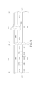
- FIG. 1 to FIG. 3 are schematic diagrams illustrating a method of forming a semiconductor device according to a first preferred embodiment of the present invention, wherein:
- FIG. 1 is a schematic cross-sectional view showing a semiconductor device after forming an opening
- FIG. 2 is a schematic cross-sectional view showing a semiconductor device after forming a tungsten layer
- FIG. 3 is a schematic cross-sectional view showing a semiconductor device after forming a metal layer.
- FIG. 4 to FIG. 6 are schematic diagrams illustrating a method of forming a semiconductor device according to a second preferred embodiment of the present invention, wherein:
- FIG. 4 is a schematic cross-sectional view showing a semiconductor device after forming a tungsten layer
- FIG. 5 is a schematic cross-sectional view showing a semiconductor device after performing a treatment process
- FIG. 6 is a schematic cross-sectional view showing a semiconductor device after forming another tungsten layer.
- FIG. 7 to FIG. 8 are schematic diagrams illustrating a method of forming a semiconductor device according to a third preferred embodiment of the present invention, wherein:
- FIG. 7 is a schematic cross-sectional view showing a semiconductor device after forming an interface layer
- FIG. 8 is a schematic cross-sectional view showing a semiconductor device after forming another tungsten layer.
- FIG. 9 to FIG. 10 are schematic diagrams illustrating a method of forming a semiconductor device according to a fourth preferred embodiment of the present invention, wherein:
- FIG. 9 is a schematic cross-sectional view showing a semiconductor device after forming an interface layer
- FIG. 10 is a schematic cross-sectional view showing a semiconductor device after forming another tungsten layer.
- a substrate 100 for example a semiconductor substrate like a silicon substrate, a silicon containing substrate or a silicon-on-insulator (SOI) substrate is provided, and two regions 101 , 102 are defined on the substrate 100 , to serve as a center region and an edge region respectively, but is not limited thereto.
- the substrate 100 includes at least one conductive region 120 formed within the region 101 , and the conductive region 120 may be any kind of conductive unit or metal contact.
- the conductive region 120 of the present embodiment may be a contact plug, a via plug or a metal line formed in a dielectric layer 110 , as shown in FIG. 1 .
- openings 140 , 160 are respectively formed in the substrate 100 , within the two regions 101 , 102 , to expose a portion of the conductive region 120 from a bottom of each opening 140 , and to expose a portion of the dielectric layer 110 from a bottom of each opening 160 .
- the openings 140 , 160 are formed in a stop layer 130 and a dielectric layer 150 stacked one over another on the substrate.
- the stop layer 130 is formed between the two dielectric layers 110 , 150 , and includes a dielectric material such as silicon oxynitride (SiON) or silicon carbonitride (SiCN), so that, the stop layer 130 may be performed like an etching stop layer while forming the openings 140 , 160 .
- the openings 140 formed in the region 101 have a relative smaller diameter d 1
- the opening 160 formed in the region 102 has a relative larger diameter d 2 , for example being two times or three times larger than the diameter d 1 , but is not limited thereto.
- a chemical vapor deposition (CVD) is performed to form a tungsten (W) layer 170 .
- CVD chemical vapor deposition
- the grain growth of tungsten are extended upwardly along the crystallization thereof, to firstly fill the openings 140 with the smaller diameter d 1 , and to further cover on a top surface of the dielectric layer 150 .
- the formed tungsten layer 170 is partially filled in the opening 160 with a larger diameter d 2 , as shown in FIG. 2 .
- the grain size of tungsten is gradually increased with the film thickness of the tungsten layer 170 .
- the tungsten layer 170 that is close to a bottom surface (namely the surface directly in contact with the conductive region 120 or the dielectric layer 110 ) thereof has a relative smaller grain size of tungsten, for example being about 1 nanometers (nm) to 10 nm
- the tungsten layer 170 that is close to a top surface (namely the surface away from the conductive region 120 or the dielectric layer 110 ) thereof has a relative larger grain size of tungsten, for example being about 80 nm to 100 nm. That is, as shown in FIG. 2 , the comparatively larger grain size of tungsten at the top surface of the tungsten layer 170 leads to a comparatively rough profile and an uneven surface 170 a of the tungsten layer 170 .
- a planarization process such as a chemical mechanical polishing/planarization (CMP) process is performed, to completely remove the tungsten layer 170 formed on the top surface of the dielectric layer 150 .
- CMP chemical mechanical polishing/planarization
- the tungsten layer 170 formed within the openings 140 may therefore obtain a planar top surface, so as to function like metal lines.
- the uneven surface 170 a thereof still remains in the opening 160 without being removed in the aforementioned CMP process.
- the tungsten layer 170 formed within the opening 160 is then functions like an alignment mark in the subsequent process.
- a conductive layer 190 such as an aluminum (Al) layer is formed on the dielectric layer 150 , to cover the tungsten layer 170 within the two regions 101 , 102 .
- the conductive layer 190 formed within the region 102 may also have a comparative rough, uneven surface 190 a due to the uneven surface 170 a of the tungsten layer 170 disposed underneath.
- the conductive layer 190 disposed within the region 101 may be patterned, and a protection layer such as a passivation layer (not shown in the drawings) may be formed then.
- the patterned conductive layer (not shown in the drawings) directly contacts the conductive region 120 underneath, and a portion of the dielectric layer 150 may therefore be exposed from the patterned conductive layer. That is, the protection layer may cover on the entire conductive layer 190 within the region 102 , and the patterned conductive layer and the exposed dielectric layer 150 within the region 101 , with a portion (not shown in the drawings) of the conductive layer 190 being exposed from the protection layer.
- connection element such as a solder bond (not shown in the drawings) may be formed via a package process like surface-mount technology (SMT), to electrically connect the exposed portion of the conductive layer 190 to other elements.
- SMT surface-mount technology
- the tungsten layer 170 and the conductive layer 190 formed within the region 102 are not electrically connected to any element, so as to serve as an alignment mark in a subsequent lithography or dicing process.
- the method of forming a semiconductor device in the first preferred embodiment is completed.
- the CVD process is used to form the tungsten layer 170 , to completely fill the openings 140 with a smaller diameter and to partially fill the opening 160 with a larger diameter.
- the conductive layer is formed after performing the planarization process, to make the tungsten layer 170 disposed within the openings 140 , 160 to function like a metal line and an alignment mark respectively.
- the semiconductor device obtained through the aforementioned forming method includes the dielectric layer 150 disposed on the substrate 100 , the openings 140 , 160 with different diameters in the dielectric layer 150 , the tungsten layer 170 disposed in the openings 140 , 160 , and the conductive layer 190 disposed on the tungsten layer 170 . It is noted that, the tungsten layer 170 completely fills the openings 140 and only partially fills the opening 160 , and the grain size of tungsten is gradually increased from the bottom surface of the tungsten layer 170 to the top surface of the tungsten layer 170 of the tungsten layer 170 .
- the conductive layer 190 disposed on such uneven surface 170 a of the tungsten layer 170 also has the comparatively rough, uneven surface 190 a , and such rough, uneven profile of the conductive layer 190 and the tungsten layer 170 may easily affect the normal function of the alignment mark during the subsequent dicing process.
- the uneven surface may be improved by reducing the film thickness of the conductive layer 190
- the reduced film thickness of the conductive layer 190 may further lead to induced resistance that is harmful to device performance.
- the semiconductor device and the forming method thereof may also have other example, and are not limited to the aforementioned embodiment.
- the following description will detail other different embodiments or variant embodiments of the semiconductor device and the forming method thereof in the present invention. To simplify the description, the following description will detail the dissimilarities among the different embodiments and the identical features will not be redundantly described. In order to compare the differences between the embodiments easily, the identical components in each of the following embodiments are marked with identical symbols.
- FIG. 4 to FIG. 6 a method of forming a semiconductor device according to the second preferred embodiment of the present invention is shown.
- the formal steps in the present embodiment are substantially similar to those shown in FIG. 1 of the first preferred embodiment, and which will not be redundantly described hereinafter.
- the differences between the present embodiment and the aforementioned first preferred embodiment are that, the tungsten layer is formed through a two-step CVD process.
- a first step of CVD process is performed to form a tungsten layer 370 , with the film thickness thereof to completely fill in the openings 140 and further cover on surfaces of the dielectric layer 150 and the opening 160 , as shown in FIG. 4 .
- the grain growth of tungsten are extended upwardly along the crystallization while forming the tungsten layer 370 , and the grain size of tungsten is also gradually increased with the film thickness of the tungsten layer 370 .
- the tungsten layer 370 that is close to a bottom surface (namely the surface directly in contact with the conductive region 120 or the dielectric layer 110 ) thereof has a relative smaller grain size of tungsten, for example being about 1 nm to 10 nm
- the tungsten layer 370 that is close to a top surface (namely the surface away from the conductive region 120 or the dielectric layer 110 ) thereof has a relative larger grain size of tungsten, for example being about 20 nm to 50 nm.
- the tungsten layer 370 of the present embodiment includes a relative smaller thickness in comparison with that of the tungsten layer 170 of the first embodiment.
- the thickness of the tungsten layer 370 is about 50 nm to 100 nm, and which is about a half of the entire thickness of the tungsten layer 170 (such as about 100 nm to 200 nm), but is not limited thereto.
- the grain size of tungsten at the top surface of the tungsten layer 370 is larger than that at any other portion of the tungsten layer 370 , such grain size of tungsten is still smaller than the grain size of tungsten at the top surface of the tungsten layer 170 . That is, the grain size of tungsten at the top surface of the tungsten layer 370 may not lead to comparatively rough profile or an uneven surface of the tungsten layer 370 , as shown in FIG. 4 .
- a treatment process P 1 is performed, to interact with the grain growth of tungsten at the top surface of the tungsten layer 370 .
- a suitable gas or radicals are introduced to the top surface of the tungsten layer 370 , to interfere with the crystallization thereof. With such performance, the grain growth of tungsten at the top surface of the tungsten layer 370 is therefore transformed to amorphous tungsten.
- the gas or the radicals includes an oxygen-containing gas or an oxygen-containing radical
- the oxygen-containing gas is for example selected from one of a group including oxygen (O 2 ), ozone (O 3 ) and nitric oxide (NO)
- the oxygen-containing radical is for example selected from one of a group including oxygen radical and oxygen plasma, nitric oxide radical.
- the gas or the radicals includes an nitrogen-containing gas or an nitrogen-containing radical
- the nitrogen-containing gas is for example selected from one of a group including nitrogen (N 2 ), NO, nitrous oxide (N 2 O), nitric dioxide (NO 2 ), ammonia (NH 3 ) and hydrazine (N 2 H 4 )
- the nitrogen-containing radical is for example selected from one of a group including nitrogen radical, NO radical, NH radical, and NH 2 radical.
- a processing temperature of the treatment process P 1 is set at approximately between 300° C. and 1,000° C., preferably between 300° C.
- the substrate 100 is heated during the treatment process P 1 , so as to maintain the temperature of the substrate 100 at about 300° C. to 1,000° C., but is not limited thereto.
- a second step of CVD process is performed, to form a tungsten layer 375 , and the entire thickness of the two tungsten layers 370 , 375 is substantially equal to the thickness (being about 100 nm to 200 nm) of the tungsten layer 170 in the first embodiment, or slightly slight greater than the thickness of the tungsten layer 170 in the first embodiment, such as being about 250 nm.
- the gas or the radical are completely removed for example by selectively performing a physical or a chemical removing process to clean any residue of the gas or the radicals remained on the tungsten layer 370 , followed by forming the tungsten layer 375 right on the tungsten layer 370 .
- the grain growth of tungsten at the top surface of the tungsten layer 370 has been inhibited and then transformed into amorphous tungsten
- the grain growth of tungsten of the tungsten layer 375 may be recrystallized instead of continuously extending along the original crystallization of the tungsten layer 370 .
- the grain size of tungsten of the tungsten layer 375 may not be continuously increased along the original crystallization of the tungsten layer 370 .
- the tungsten layer 375 that is close to a bottom surface (namely the surface directly in contact with the tungsten layer 370 ) thereof has a relative smaller grain size of tungsten, for example being about 1 nm to 10 nm, and the grain sized of tungsten of the tungsten layer 375 is also gradually increased with the film thickness.
- the tungsten layer 375 that is close to a top surface (namely the surface away from the tungsten layer 370 ) thereof has a relative larger grain size of tungsten, for example being about 50 nm to 70 nm.
- the grain growth of tungsten at the top surface of the tungsten layer 375 may not have issues of the oversized grain, so as to prevent from the comparatively rough profile or an uneven surface, as shown in FIG. 6 .
- the method of forming a semiconductor device in the second preferred embodiment is completed.
- the two-step CVD process is performed to form the tungsten layers 370 , 375 , and the treatment process P 1 is further performed between the two CVD processes to inhibit the grain growth of tungsten at the top surface of the tungsten layer 370 .
- the entire thickness of the two tungsten layers 370 , 375 is substantially equal to that of the tungsten layer 170 , the grain size of tungsten at the top surface of the tungsten layer 375 is sufficiently reduced for avoiding the comparative rough, uneven surface that occurred to the tungsten layer 375 .
- the planarization process, the formation of the conductive layer 190 , and the subsequent package and dicing processes as described in the first preferred embodiment may also be conducted.
- issues of the comparatively rough profile or the uneven surface happened on the tungsten layer 375 and the conductive layer formed thereon may both be improved, so that, the subsequent processes such as the dicing process will no longer be affected by these issues. Then, a better element performance may therefore be achieved.
- the semiconductor device obtained through the aforementioned forming method includes the dielectric layer 150 disposed on the substrate 100 , the openings 140 , 160 with different diameters in the dielectric layer 150 , the tungsten layer 370 disposed in the openings 140 , 160 , and the tungsten layer 375 disposed on the tungsten layer 370 .
- the tungsten layer 370 completely fills the openings 140 and only partially fills the opening 160
- the tungsten layer 375 is directly in contact with the top surface of the tungsten layer 370 to partially fill in the opening 160 .
- the grain sizes of the two tungsten layers 370 , 375 are both gradually increased from the bottom surface to the top surface thereof, and the grain growth of tungsten at the top surface of the tungsten layer 370 is transformed to amorphous tungsten, so as to form an interface layer (not shown in the drawings of the present embodiment) between the two tungsten layers 370 , 375 . That is, the tungsten layer 370 , the interface layer and the tungsten layer 375 stacked one over another in the opening 160 may therefore form a tungsten stacked structure.
- the semiconductor device obtained from the present embodiment is capable of improving the issues of the comparatively rough profile or the uneven surface of the tungsten layer caused by the oversized grain of tungsten, so as to gain better element performance.
- FIG. 7 to FIG. 8 a method of forming a semiconductor device according to the third preferred embodiment of the present invention is shown.
- the formal steps in the present embodiment are substantially similar to those shown in FIG. 1 , FIG. 4 of the aforementioned first and the second preferred embodiments, and which will not be redundantly described hereinafter.
- the differences between the present embodiment and the aforementioned two embodiments are that, the removing process after the treatment process P 1 is omitted or the processing parameters, such as the processing temperature, the processing pressure, the process time for inducing gas or radicals, or the processing gas flow, of the treatment process P 1 are modified to let a portion of the gas or the radicals remain on the top surface of the tungsten layer 370 , to form an interface layer 390 thereby.
- the treatment process P 2 of the present embodiment is also performed to inhibit the grain growth of tungsten at the top surface of the tungsten layer 370 , and to let a portion of the gas or the radicals remain on the tungsten layer 370 to form the interface layer 390 as shown in FIG. 7 .
- the gas or the radicals include the oxygen-containing gas or the oxygen-containing radical
- the interface layer 390 may include an oxygen-containing layer including remaining oxygen, oxygen plasma or oxygen radical.
- the gas or the radicals include the nitrogen-containing gas or the nitrogen-containing radical
- the interface layer 390 may include a nitrogen-containing layer including nitrogen, or nitrogen radical.
- the interface layer 390 includes the gas or the radical residue from the treatment process P 2 , which may further inhibit the grain growth of tungsten at the top surface of the tungsten layer 370 . That is, the grain growth of tungsten of the tungsten layer 375 may be recrystallized instead of continuously extending along the original crystallization of the tungsten layer 370 , so as to obtain a relative smaller grain size.
- the tungsten layer 375 that is close to a bottom surface (namely the surface directly in contact with the interface layer 390 ) thereof has a relative smaller grain size of tungsten, for example being about 1 nm to 10 nm, and the grain sized of tungsten of the tungsten layer 375 is also gradually increased with the film thickness.
- the tungsten layer 375 that is close to a top surface (namely the surface away from the interface layer 390 ) thereof has a relative larger grain size of tungsten, for example being about 50 nm to 70 nm.
- the grain growth of tungsten at the top surface of the tungsten layer 375 may not have issues of the oversized grain, so as to effectively prevent from comparatively rough profile or an uneven surface, as shown in FIG. 8 .
- the method of forming a semiconductor device in the third preferred embodiment is completed.
- the two-step CVD process is performed to form the tungsten layers 370 , 375
- the treatment process P 2 is further performed between the two CVD processes to form the interface layer 390 between the two tungsten layers 370 , 375 .
- the interface layer 390 formed in the present embodiment may further improve the oversized grain of tungsten.
- the interface layer 390 has an extremely small thickness, so that, the entire thickness of the interface layer 390 and the two tungsten layers 370 , 375 is still substantially equal to that of the tungsten layer 170 .
- the planarization process, the formation of the conductive layer 190 , and the subsequent package and dicing processes as described in the first preferred embodiment may also be conducted.
- the issues of the comparatively rough profile or the uneven surface happened on the tungsten layer 375 and the conductive layer formed thereon are both be improved, so that, the subsequent processes such as the dicing process will no longer be affected by these issues. In this way, a better element performance may therefore achieve.
- the semiconductor device obtained through the aforementioned forming method includes the dielectric layer 150 disposed on the substrate 100 , the openings 140 , 160 with different diameters in the dielectric layer 150 , the tungsten layer 370 disposed in the openings 140 , 160 , and the tungsten layer 375 disposed on the tungsten layer 370 .
- the tungsten layer 370 completely fills the openings 140 and only partially fills the opening 160
- the tungsten layer 375 is directly in contact with the top surface of the tungsten layer 370 to partially fill in the opening 160 .
- the grain sizes of the two tungsten layers 370 , 375 are both gradually increased from the bottom surface to the top surface thereof, and the grain growth of tungsten at the top surface of the tungsten layer 370 is transformed to amorphous tungsten, so as to form an interface layer 390 between the two tungsten layers 370 , 375 . That is, the tungsten layer 370 , the interface layer and the tungsten layer 375 stacked one over another in the opening 160 may therefore form a tungsten stacked structure. Also, since the grain size of tungsten at the top surface of the tungsten layer 375 is about 50 nm to 70 nm, the comparatively rough, uneven surface may no longer present on the tungsten layer 375 . Therefore, the semiconductor device obtain from the present embodiment is capable of improving the issues of the comparatively rough profile or the uneven surface of the tungsten layer caused by the oversized grain of tungsten, so as to gain better element performance.
- FIG. 9 to FIG. 10 a method of forming a semiconductor device according to the fourth preferred embodiment of the present invention is shown.
- the formal steps in the present embodiment are substantially similar to those shown in FIG. 1 , FIG. 4 of the aforementioned second preferred embodiment, and which will not be redundantly descried hereinafter.
- the differences between the present embodiment and the aforementioned third embodiment are that, the processing parameters, such as the processing temperature, the processing pressure, the process time for inducing gas or radicals, or the processing gas flow, of the treatment process P 2 are modified to let a portion of the gas or the radicals to react with tungsten at the top surface of the tungsten layer 370 , to form an interface layer 395 thereby.
- the treatment process P 3 of the present embodiment is also performed to inhibit the grain growth of tungsten at the top surface of the tungsten layer 370 , to transform the tungsten into amorphous tungsten, and to let a portion of the gas or the radicals remain on the tungsten layer 370 to form the interface layer 395 as shown in FIG. 9 .
- the gas or the radicals include the oxygen-containing gas or the oxygen-containing radical
- the interface layer 395 may include an oxygen-containing layer for example including tungsten oxide (WO), or tungsten oxynitride (WNO).
- the gas or the radicals include the nitrogen-containing gas or the nitrogen-containing radical
- the interface layer 395 may include a nitrogen-containing layer for example including tungsten nitride (WN) or WNO.
- the grain sizes of WN, WNO, or WO are smaller than that of tungsten, so that, the grain growth of tungsten of the tungsten layer 375 may still be recrystallized instead of continuously extending along the original crystallization of the tungsten layer 370 .
- the tungsten layer 375 that is close to a bottom surface (namely the surface directly in contact with the interface layer 395 ) thereof has a relative smaller grain size of tungsten, for example being about 1 nm to 10 nm, and the grain sized of tungsten of the tungsten layer 375 is also gradually increased with the film thickness.
- the tungsten layer 375 that is close to a top surface (namely the surface away from the interface layer 395 ) thereof has a relative larger grain size of tungsten, for example being about 50 nm to 70 nm.
- the grain growth of tungsten at the top surface of the tungsten layer 375 may not have issues of the oversized grain, so as to effectively prevent the comparatively rough profile or an uneven surface, as shown in FIG. 10 .
- the method of forming a semiconductor device in the fourth preferred embodiment is completed.
- the two-step CVD process is performed to form the tungsten layers 370 , 375
- the treatment process P 3 is further performed between the two CVD processes to form the interface layer 395 between the two tungsten layers 370 , 375 .
- the interface layer 395 formed in the present embodiment may further improve the oversized grain of tungsten.
- the interface layer 395 has a relative smaller thickness in comparison with that of the two tungsten layers 370 , 375 , such as being about 10 angstroms to 20 angstroms, so that, the entire thickness of the interface layer 395 and the two tungsten layers 370 , 375 is still substantially equal to that of the tungsten layer 170 .
- the planarization process, the formation of the conductive layer 190 , and the subsequent package and dicing processes as described in the first preferred embodiment may also be conducted.
- the issues of the comparatively rough profile or the uneven surface that occurred on the tungsten layer 375 and the conductive layer formed thereon are both be improved, so that, the subsequent processes such as the dicing process will no longer be affected by these issues. In this way, a better element performance may therefore be achieved.
- the semiconductor device obtained through the aforementioned forming method includes the dielectric layer 150 disposed on the substrate 100 , the openings 140 , 160 with different diameters in the dielectric layer 150 , the tungsten layer 370 disposed in the openings 140 , 160 , and the tungsten layer 375 disposed on the tungsten layer 370 .
- the openings 140 are completely filled by the tungsten layer 370 , and the interface layer 395 and the tungsten layer 375 are stacked thereon.
- the tungsten layer 370 , the interface layer and the tungsten layer 375 are stacked one over another in the opening 160 , to form a tungsten stacked structure, and the tungsten stacked structure only partially fills the opening 160 . Therefore, the semiconductor device obtained from the present embodiment is capable of improving the issues of the comparatively rough profile or the uneven surface of the tungsten layer caused by the oversized grain of tungsten, so as to gain better element performance.
- the present invention utilizes a two-step CVD process to form two tungsten layers, and further utilizes a treatment process between the two CVD processes to inhibit the grain growth of tungsten by introducing a suitable gas or radicals to a top surface of the bottom tungsten layer to interfere with the original crystallization, and to transfer the grain growth of tungsten thereof into amorphous tungsten. That is, the top tungsten layer deposited on the bottom tungsten layer may be recrystallized to obtain a relative smaller grain size instead of continuously extended along the original crystallization of the bottom tungsten layer.
- the forming method of the present invention is capable of improving issues of the oversized grain of the top tungsten layer, and the subsequent processes such as the dicing process will no longer be affected by these issues. In this way, the semiconductor device obtained via aforementioned forming method in the present invention may therefore gain a better element performance.
Landscapes
- Chemical & Material Sciences (AREA)
- Engineering & Computer Science (AREA)
- General Chemical & Material Sciences (AREA)
- Chemical Kinetics & Catalysis (AREA)
- Metallurgy (AREA)
- Mechanical Engineering (AREA)
- Materials Engineering (AREA)
- Organic Chemistry (AREA)
- Physics & Mathematics (AREA)
- Electromagnetism (AREA)
- Plasma & Fusion (AREA)
- Inorganic Chemistry (AREA)
- Internal Circuitry In Semiconductor Integrated Circuit Devices (AREA)
- Electrodes Of Semiconductors (AREA)
Abstract
Description
Claims (10)
Applications Claiming Priority (3)
| Application Number | Priority Date | Filing Date | Title |
|---|---|---|---|
| CN201810133700 | 2018-02-09 | ||
| CN201810133700.6A CN110137153B (en) | 2018-02-09 | 2018-02-09 | Semiconductor device and method of forming the same |
| CN201810133700.6 | 2018-02-09 |
Publications (2)
| Publication Number | Publication Date |
|---|---|
| US20190249297A1 US20190249297A1 (en) | 2019-08-15 |
| US10465287B2 true US10465287B2 (en) | 2019-11-05 |
Family
ID=67540376
Family Applications (1)
| Application Number | Title | Priority Date | Filing Date |
|---|---|---|---|
| US15/919,191 Active US10465287B2 (en) | 2018-02-09 | 2018-03-12 | Semiconductor device and method of forming the same |
Country Status (2)
| Country | Link |
|---|---|
| US (1) | US10465287B2 (en) |
| CN (1) | CN110137153B (en) |
Families Citing this family (1)
| Publication number | Priority date | Publication date | Assignee | Title |
|---|---|---|---|---|
| WO2016046909A1 (en) * | 2014-09-24 | 2016-03-31 | 株式会社日立国際電気 | Method for manufacturing semiconductor device, substrate processing apparatus, semiconductor device and program |
Citations (22)
| Publication number | Priority date | Publication date | Assignee | Title |
|---|---|---|---|---|
| US5407698A (en) * | 1992-04-29 | 1995-04-18 | Northern Telecom Limited | Deposition of tungsten |
| US5686355A (en) * | 1994-10-27 | 1997-11-11 | Sony Corporation | Method for forming film of refractory metal |
| US5731225A (en) * | 1995-04-27 | 1998-03-24 | Nec Corporation | Method for fabricating semiconductor device having buried contact structure |
| US5804249A (en) * | 1997-02-07 | 1998-09-08 | Lsi Logic Corporation | Multistep tungsten CVD process with amorphization step |
| US5956609A (en) * | 1997-08-11 | 1999-09-21 | Taiwan Semiconductor Manufacturing Company, Ltd. | Method for reducing stress and improving step-coverage of tungsten interconnects and plugs |
| US6331483B1 (en) * | 1998-12-18 | 2001-12-18 | Tokyo Electron Limited | Method of film-forming of tungsten |
| US6413853B2 (en) * | 2000-01-06 | 2002-07-02 | Samsung Electronics Co., Ltd. | Method of forming a tungsten plug in a semiconductor device |
| US6475907B1 (en) * | 1999-04-20 | 2002-11-05 | Nec Corporation | Semiconductor device having a barrier metal layer and method for manufacturing the same |
| US6498095B2 (en) * | 1998-03-16 | 2002-12-24 | Nec Corporation | Cvd method for producing an interconnection film by depositing a lower layer to fill a recess performing a cleaning step to remove dissociated reactant gas, and consequently depositing an upper layer that has a smaller impurity concentration than the lower layer |
| US6524956B1 (en) * | 1999-09-24 | 2003-02-25 | Novelius Systems, Inc. | Method for controlling the grain size of tungsten films |
| US6579788B1 (en) * | 2000-09-18 | 2003-06-17 | Advanced Micro Devices, Inc. | Method of forming conductive interconnections on an integrated circuit device |
| US20030198086A1 (en) * | 2002-04-18 | 2003-10-23 | Shoji Shukuri | Semiconductor integrated circuit device and a method of manufacturing the same |
| US6645863B2 (en) | 2001-05-25 | 2003-11-11 | Mitsubishi Denki Kabushiki Kaisha | Method of manufacturing semiconductor device and semiconductor device |
| US20050029010A1 (en) * | 2003-08-04 | 2005-02-10 | Jeong-Hoon Ahn | Void-free metal interconnection steucture and method of forming the same |
| US20050272258A1 (en) * | 2004-06-04 | 2005-12-08 | Toshiyuki Morita | Method of manufacturing a semiconductor device and semiconductor device |
| US7005372B2 (en) | 2003-01-21 | 2006-02-28 | Novellus Systems, Inc. | Deposition of tungsten nitride |
| US7233073B2 (en) * | 2003-07-31 | 2007-06-19 | Matsushita Electric Industrial Co., Ltd. | Semiconductor device and method for fabricating the same |
| US20090238958A1 (en) * | 2008-03-20 | 2009-09-24 | Nishant Sinha | Methods of Forming Electrically Conductive Structures |
| US7795137B2 (en) * | 2005-08-26 | 2010-09-14 | Hitachi, Ltd. | Manufacturing method of semiconductor device |
| US20170125354A1 (en) * | 2015-11-03 | 2017-05-04 | Semiconductor Manufacturing International Shanghai) Corp | Conductive plug structure and fabrication method thereof |
| US9704919B1 (en) * | 2016-06-24 | 2017-07-11 | Qualcomm Incorporated | High aspect ratio vertical interconnect access (via) interconnections in magnetic random access memory (MRAM) bit cells |
| US10256142B2 (en) * | 2009-08-04 | 2019-04-09 | Novellus Systems, Inc. | Tungsten feature fill with nucleation inhibition |
-
2018
- 2018-02-09 CN CN201810133700.6A patent/CN110137153B/en active Active
- 2018-03-12 US US15/919,191 patent/US10465287B2/en active Active
Patent Citations (22)
| Publication number | Priority date | Publication date | Assignee | Title |
|---|---|---|---|---|
| US5407698A (en) * | 1992-04-29 | 1995-04-18 | Northern Telecom Limited | Deposition of tungsten |
| US5686355A (en) * | 1994-10-27 | 1997-11-11 | Sony Corporation | Method for forming film of refractory metal |
| US5731225A (en) * | 1995-04-27 | 1998-03-24 | Nec Corporation | Method for fabricating semiconductor device having buried contact structure |
| US5804249A (en) * | 1997-02-07 | 1998-09-08 | Lsi Logic Corporation | Multistep tungsten CVD process with amorphization step |
| US5956609A (en) * | 1997-08-11 | 1999-09-21 | Taiwan Semiconductor Manufacturing Company, Ltd. | Method for reducing stress and improving step-coverage of tungsten interconnects and plugs |
| US6498095B2 (en) * | 1998-03-16 | 2002-12-24 | Nec Corporation | Cvd method for producing an interconnection film by depositing a lower layer to fill a recess performing a cleaning step to remove dissociated reactant gas, and consequently depositing an upper layer that has a smaller impurity concentration than the lower layer |
| US6331483B1 (en) * | 1998-12-18 | 2001-12-18 | Tokyo Electron Limited | Method of film-forming of tungsten |
| US6475907B1 (en) * | 1999-04-20 | 2002-11-05 | Nec Corporation | Semiconductor device having a barrier metal layer and method for manufacturing the same |
| US6524956B1 (en) * | 1999-09-24 | 2003-02-25 | Novelius Systems, Inc. | Method for controlling the grain size of tungsten films |
| US6413853B2 (en) * | 2000-01-06 | 2002-07-02 | Samsung Electronics Co., Ltd. | Method of forming a tungsten plug in a semiconductor device |
| US6579788B1 (en) * | 2000-09-18 | 2003-06-17 | Advanced Micro Devices, Inc. | Method of forming conductive interconnections on an integrated circuit device |
| US6645863B2 (en) | 2001-05-25 | 2003-11-11 | Mitsubishi Denki Kabushiki Kaisha | Method of manufacturing semiconductor device and semiconductor device |
| US20030198086A1 (en) * | 2002-04-18 | 2003-10-23 | Shoji Shukuri | Semiconductor integrated circuit device and a method of manufacturing the same |
| US7005372B2 (en) | 2003-01-21 | 2006-02-28 | Novellus Systems, Inc. | Deposition of tungsten nitride |
| US7233073B2 (en) * | 2003-07-31 | 2007-06-19 | Matsushita Electric Industrial Co., Ltd. | Semiconductor device and method for fabricating the same |
| US20050029010A1 (en) * | 2003-08-04 | 2005-02-10 | Jeong-Hoon Ahn | Void-free metal interconnection steucture and method of forming the same |
| US20050272258A1 (en) * | 2004-06-04 | 2005-12-08 | Toshiyuki Morita | Method of manufacturing a semiconductor device and semiconductor device |
| US7795137B2 (en) * | 2005-08-26 | 2010-09-14 | Hitachi, Ltd. | Manufacturing method of semiconductor device |
| US20090238958A1 (en) * | 2008-03-20 | 2009-09-24 | Nishant Sinha | Methods of Forming Electrically Conductive Structures |
| US10256142B2 (en) * | 2009-08-04 | 2019-04-09 | Novellus Systems, Inc. | Tungsten feature fill with nucleation inhibition |
| US20170125354A1 (en) * | 2015-11-03 | 2017-05-04 | Semiconductor Manufacturing International Shanghai) Corp | Conductive plug structure and fabrication method thereof |
| US9704919B1 (en) * | 2016-06-24 | 2017-07-11 | Qualcomm Incorporated | High aspect ratio vertical interconnect access (via) interconnections in magnetic random access memory (MRAM) bit cells |
Also Published As
| Publication number | Publication date |
|---|---|
| CN110137153B (en) | 2021-03-30 |
| US20190249297A1 (en) | 2019-08-15 |
| CN110137153A (en) | 2019-08-16 |
Similar Documents
| Publication | Publication Date | Title |
|---|---|---|
| TWI536497B (en) | Semiconductor device manufacturing method and semiconductor device | |
| US8664769B2 (en) | Semiconductor device | |
| KR101129919B1 (en) | Semiconductor device and method for forming the same | |
| US20200098922A1 (en) | Semiconductor device and method of manufacturing the same | |
| TWI566362B (en) | Semiconductor device and method of manufacturing the same | |
| US12255095B2 (en) | Semiconductor structure and manufacturing method thereof | |
| US10580665B2 (en) | Method for manufacturing package structure having elastic bump | |
| US6541863B1 (en) | Semiconductor device having a reduced signal processing time and a method of fabricating the same | |
| US10199269B2 (en) | Conductive structure and method for manufacturing conductive structure | |
| US20070224797A1 (en) | Method for manufacturing semiconductor device, method for forming alignment mark, and semiconductor device | |
| US10465287B2 (en) | Semiconductor device and method of forming the same | |
| US10276648B1 (en) | Plasma treatment for thin film resistors on integrated circuits | |
| US20160104636A1 (en) | Semiconductor device and method of manufacturing the same | |
| US7897466B2 (en) | Method for manufacturing semiconductor device | |
| TWI576959B (en) | Method of forming semiconductor structure having contact plug | |
| US20070013076A1 (en) | Semiconductor device and method of manufacturing thereof | |
| US10340283B2 (en) | Process for fabricating 3D memory | |
| CN108231666B (en) | Semiconductor device with integrated electronic fuse and method of forming the same | |
| US20160133572A1 (en) | Methods of forming a protective layer on an insulating layer for protection during formation of conductive structures | |
| US9209071B2 (en) | Semiconductor structure with anti-etch structure in via and method for manufacturing the same | |
| US20030036276A1 (en) | Method for forming high resistance resistor with integrated high voltage device process | |
| TWI888982B (en) | Semiconductor device and method for manufacturing semiconductor device | |
| US20250072013A1 (en) | Resistor structure with capping structure on tfr layer | |
| CN115346915A (en) | Method for manufacturing semiconductor device | |
| KR100545900B1 (en) | Semiconductor device manufacturing method |
Legal Events
| Date | Code | Title | Description |
|---|---|---|---|
| AS | Assignment |
Owner name: FUJIAN JINHUA INTEGRATED CIRCUIT CO., LTD., CHINA Free format text: ASSIGNMENT OF ASSIGNORS INTEREST;ASSIGNORS:LIU, CHIH-CHIEN;CHEN, PIN-HONG;CHENG, TSUN-MIN;AND OTHERS;REEL/FRAME:045180/0534 Effective date: 20180307 Owner name: UNITED MICROELECTRONICS CORP., TAIWAN Free format text: ASSIGNMENT OF ASSIGNORS INTEREST;ASSIGNORS:LIU, CHIH-CHIEN;CHEN, PIN-HONG;CHENG, TSUN-MIN;AND OTHERS;REEL/FRAME:045180/0534 Effective date: 20180307 |
|
| FEPP | Fee payment procedure |
Free format text: ENTITY STATUS SET TO UNDISCOUNTED (ORIGINAL EVENT CODE: BIG.); ENTITY STATUS OF PATENT OWNER: LARGE ENTITY |
|
| STPP | Information on status: patent application and granting procedure in general |
Free format text: NOTICE OF ALLOWANCE MAILED -- APPLICATION RECEIVED IN OFFICE OF PUBLICATIONS |
|
| STPP | Information on status: patent application and granting procedure in general |
Free format text: PUBLICATIONS -- ISSUE FEE PAYMENT VERIFIED |
|
| STCF | Information on status: patent grant |
Free format text: PATENTED CASE |
|
| CC | Certificate of correction | ||
| MAFP | Maintenance fee payment |
Free format text: PAYMENT OF MAINTENANCE FEE, 4TH YEAR, LARGE ENTITY (ORIGINAL EVENT CODE: M1551); ENTITY STATUS OF PATENT OWNER: LARGE ENTITY Year of fee payment: 4 |