US10453750B2 - Stacked elongated nanoshapes of different semiconductor materials and structures that incorporate the nanoshapes - Google Patents
Stacked elongated nanoshapes of different semiconductor materials and structures that incorporate the nanoshapes Download PDFInfo
- Publication number
- US10453750B2 US10453750B2 US15/629,884 US201715629884A US10453750B2 US 10453750 B2 US10453750 B2 US 10453750B2 US 201715629884 A US201715629884 A US 201715629884A US 10453750 B2 US10453750 B2 US 10453750B2
- Authority
- US
- United States
- Prior art keywords
- nanoshape
- semiconductor material
- forming
- semiconductor
- substrate
- Prior art date
- Legal status (The legal status is an assumption and is not a legal conclusion. Google has not performed a legal analysis and makes no representation as to the accuracy of the status listed.)
- Active
Links
Images


Classifications
-
- H01L21/823431—
-
- H—ELECTRICITY
- H10—SEMICONDUCTOR DEVICES; ELECTRIC SOLID-STATE DEVICES NOT OTHERWISE PROVIDED FOR
- H10D—INORGANIC ELECTRIC SEMICONDUCTOR DEVICES
- H10D30/00—Field-effect transistors [FET]
- H10D30/01—Manufacture or treatment
- H10D30/021—Manufacture or treatment of FETs having insulated gates [IGFET]
-
- B—PERFORMING OPERATIONS; TRANSPORTING
- B82—NANOTECHNOLOGY
- B82Y—SPECIFIC USES OR APPLICATIONS OF NANOSTRUCTURES; MEASUREMENT OR ANALYSIS OF NANOSTRUCTURES; MANUFACTURE OR TREATMENT OF NANOSTRUCTURES
- B82Y10/00—Nanotechnology for information processing, storage or transmission, e.g. quantum computing or single electron logic
-
- H—ELECTRICITY
- H01—ELECTRIC ELEMENTS
- H01L—SEMICONDUCTOR DEVICES NOT COVERED BY CLASS H10
- H01L21/00—Processes or apparatus adapted for the manufacture or treatment of semiconductor or solid state devices or of parts thereof
- H01L21/02—Manufacture or treatment of semiconductor devices or of parts thereof
- H01L21/02104—Forming layers
- H01L21/02365—Forming inorganic semiconducting materials on a substrate
- H01L21/02436—Intermediate layers between substrates and deposited layers
- H01L21/02439—Materials
- H01L21/02488—Insulating materials
-
- H—ELECTRICITY
- H01—ELECTRIC ELEMENTS
- H01L—SEMICONDUCTOR DEVICES NOT COVERED BY CLASS H10
- H01L21/00—Processes or apparatus adapted for the manufacture or treatment of semiconductor or solid state devices or of parts thereof
- H01L21/02—Manufacture or treatment of semiconductor devices or of parts thereof
- H01L21/02104—Forming layers
- H01L21/02365—Forming inorganic semiconducting materials on a substrate
- H01L21/02518—Deposited layers
- H01L21/02521—Materials
- H01L21/02524—Group 14 semiconducting materials
- H01L21/02532—Silicon, silicon germanium, germanium
-
- H—ELECTRICITY
- H01—ELECTRIC ELEMENTS
- H01L—SEMICONDUCTOR DEVICES NOT COVERED BY CLASS H10
- H01L21/00—Processes or apparatus adapted for the manufacture or treatment of semiconductor or solid state devices or of parts thereof
- H01L21/02—Manufacture or treatment of semiconductor devices or of parts thereof
- H01L21/02104—Forming layers
- H01L21/02365—Forming inorganic semiconducting materials on a substrate
- H01L21/02656—Special treatments
- H01L21/02664—Aftertreatments
-
- H01L21/8221—
-
- H01L21/823437—
-
- H01L21/823807—
-
- H01L27/0688—
-
- H01L27/0886—
-
- H01L27/092—
-
- H01L29/0673—
-
- H01L29/42392—
-
- H01L29/66227—
-
- H01L29/66439—
-
- H01L29/775—
-
- H—ELECTRICITY
- H10—SEMICONDUCTOR DEVICES; ELECTRIC SOLID-STATE DEVICES NOT OTHERWISE PROVIDED FOR
- H10D—INORGANIC ELECTRIC SEMICONDUCTOR DEVICES
- H10D30/00—Field-effect transistors [FET]
- H10D30/01—Manufacture or treatment
- H10D30/014—Manufacture or treatment of FETs having zero-dimensional [0D] or one-dimensional [1D] channels, e.g. quantum wire FETs, single-electron transistors [SET] or Coulomb blockade transistors
-
- H—ELECTRICITY
- H10—SEMICONDUCTOR DEVICES; ELECTRIC SOLID-STATE DEVICES NOT OTHERWISE PROVIDED FOR
- H10D—INORGANIC ELECTRIC SEMICONDUCTOR DEVICES
- H10D30/00—Field-effect transistors [FET]
- H10D30/01—Manufacture or treatment
- H10D30/021—Manufacture or treatment of FETs having insulated gates [IGFET]
- H10D30/024—Manufacture or treatment of FETs having insulated gates [IGFET] of fin field-effect transistors [FinFET]
-
- H—ELECTRICITY
- H10—SEMICONDUCTOR DEVICES; ELECTRIC SOLID-STATE DEVICES NOT OTHERWISE PROVIDED FOR
- H10D—INORGANIC ELECTRIC SEMICONDUCTOR DEVICES
- H10D30/00—Field-effect transistors [FET]
- H10D30/40—FETs having zero-dimensional [0D], one-dimensional [1D] or two-dimensional [2D] charge carrier gas channels
- H10D30/43—FETs having zero-dimensional [0D], one-dimensional [1D] or two-dimensional [2D] charge carrier gas channels having 1D charge carrier gas channels, e.g. quantum wire FETs or transistors having 1D quantum-confined channels
-
- H—ELECTRICITY
- H10—SEMICONDUCTOR DEVICES; ELECTRIC SOLID-STATE DEVICES NOT OTHERWISE PROVIDED FOR
- H10D—INORGANIC ELECTRIC SEMICONDUCTOR DEVICES
- H10D30/00—Field-effect transistors [FET]
- H10D30/60—Insulated-gate field-effect transistors [IGFET]
-
- H—ELECTRICITY
- H10—SEMICONDUCTOR DEVICES; ELECTRIC SOLID-STATE DEVICES NOT OTHERWISE PROVIDED FOR
- H10D—INORGANIC ELECTRIC SEMICONDUCTOR DEVICES
- H10D30/00—Field-effect transistors [FET]
- H10D30/60—Insulated-gate field-effect transistors [IGFET]
- H10D30/62—Fin field-effect transistors [FinFET]
-
- H—ELECTRICITY
- H10—SEMICONDUCTOR DEVICES; ELECTRIC SOLID-STATE DEVICES NOT OTHERWISE PROVIDED FOR
- H10D—INORGANIC ELECTRIC SEMICONDUCTOR DEVICES
- H10D30/00—Field-effect transistors [FET]
- H10D30/60—Insulated-gate field-effect transistors [IGFET]
- H10D30/67—Thin-film transistors [TFT]
- H10D30/6729—Thin-film transistors [TFT] characterised by the electrodes
- H10D30/673—Thin-film transistors [TFT] characterised by the electrodes characterised by the shapes, relative sizes or dispositions of the gate electrodes
- H10D30/6735—Thin-film transistors [TFT] characterised by the electrodes characterised by the shapes, relative sizes or dispositions of the gate electrodes having gates fully surrounding the channels, e.g. gate-all-around
-
- H—ELECTRICITY
- H10—SEMICONDUCTOR DEVICES; ELECTRIC SOLID-STATE DEVICES NOT OTHERWISE PROVIDED FOR
- H10D—INORGANIC ELECTRIC SEMICONDUCTOR DEVICES
- H10D30/00—Field-effect transistors [FET]
- H10D30/60—Insulated-gate field-effect transistors [IGFET]
- H10D30/67—Thin-film transistors [TFT]
- H10D30/6757—Thin-film transistors [TFT] characterised by the structure of the channel, e.g. transverse or longitudinal shape or doping profile
-
- H—ELECTRICITY
- H10—SEMICONDUCTOR DEVICES; ELECTRIC SOLID-STATE DEVICES NOT OTHERWISE PROVIDED FOR
- H10D—INORGANIC ELECTRIC SEMICONDUCTOR DEVICES
- H10D48/00—Individual devices not covered by groups H10D1/00 - H10D44/00
- H10D48/01—Manufacture or treatment
- H10D48/031—Manufacture or treatment of three-or-more electrode devices
-
- H—ELECTRICITY
- H10—SEMICONDUCTOR DEVICES; ELECTRIC SOLID-STATE DEVICES NOT OTHERWISE PROVIDED FOR
- H10D—INORGANIC ELECTRIC SEMICONDUCTOR DEVICES
- H10D62/00—Semiconductor bodies, or regions thereof, of devices having potential barriers
- H10D62/10—Shapes, relative sizes or dispositions of the regions of the semiconductor bodies; Shapes of the semiconductor bodies
- H10D62/117—Shapes of semiconductor bodies
- H10D62/118—Nanostructure semiconductor bodies
- H10D62/119—Nanowire, nanosheet or nanotube semiconductor bodies
- H10D62/121—Nanowire, nanosheet or nanotube semiconductor bodies oriented parallel to substrates
-
- H—ELECTRICITY
- H10—SEMICONDUCTOR DEVICES; ELECTRIC SOLID-STATE DEVICES NOT OTHERWISE PROVIDED FOR
- H10D—INORGANIC ELECTRIC SEMICONDUCTOR DEVICES
- H10D84/00—Integrated devices formed in or on semiconductor substrates that comprise only semiconducting layers, e.g. on Si wafers or on GaAs-on-Si wafers
- H10D84/01—Manufacture or treatment
- H10D84/0123—Integrating together multiple components covered by H10D12/00 or H10D30/00, e.g. integrating multiple IGBTs
- H10D84/0126—Integrating together multiple components covered by H10D12/00 or H10D30/00, e.g. integrating multiple IGBTs the components including insulated gates, e.g. IGFETs
- H10D84/0135—Manufacturing their gate conductors
-
- H—ELECTRICITY
- H10—SEMICONDUCTOR DEVICES; ELECTRIC SOLID-STATE DEVICES NOT OTHERWISE PROVIDED FOR
- H10D—INORGANIC ELECTRIC SEMICONDUCTOR DEVICES
- H10D84/00—Integrated devices formed in or on semiconductor substrates that comprise only semiconducting layers, e.g. on Si wafers or on GaAs-on-Si wafers
- H10D84/01—Manufacture or treatment
- H10D84/0123—Integrating together multiple components covered by H10D12/00 or H10D30/00, e.g. integrating multiple IGBTs
- H10D84/0126—Integrating together multiple components covered by H10D12/00 or H10D30/00, e.g. integrating multiple IGBTs the components including insulated gates, e.g. IGFETs
- H10D84/0158—Integrating together multiple components covered by H10D12/00 or H10D30/00, e.g. integrating multiple IGBTs the components including insulated gates, e.g. IGFETs the components including FinFETs
-
- H—ELECTRICITY
- H10—SEMICONDUCTOR DEVICES; ELECTRIC SOLID-STATE DEVICES NOT OTHERWISE PROVIDED FOR
- H10D—INORGANIC ELECTRIC SEMICONDUCTOR DEVICES
- H10D84/00—Integrated devices formed in or on semiconductor substrates that comprise only semiconducting layers, e.g. on Si wafers or on GaAs-on-Si wafers
- H10D84/01—Manufacture or treatment
- H10D84/0123—Integrating together multiple components covered by H10D12/00 or H10D30/00, e.g. integrating multiple IGBTs
- H10D84/0126—Integrating together multiple components covered by H10D12/00 or H10D30/00, e.g. integrating multiple IGBTs the components including insulated gates, e.g. IGFETs
- H10D84/0165—Integrating together multiple components covered by H10D12/00 or H10D30/00, e.g. integrating multiple IGBTs the components including insulated gates, e.g. IGFETs the components including complementary IGFETs, e.g. CMOS devices
- H10D84/0167—Manufacturing their channels
-
- H—ELECTRICITY
- H10—SEMICONDUCTOR DEVICES; ELECTRIC SOLID-STATE DEVICES NOT OTHERWISE PROVIDED FOR
- H10D—INORGANIC ELECTRIC SEMICONDUCTOR DEVICES
- H10D84/00—Integrated devices formed in or on semiconductor substrates that comprise only semiconducting layers, e.g. on Si wafers or on GaAs-on-Si wafers
- H10D84/01—Manufacture or treatment
- H10D84/02—Manufacture or treatment characterised by using material-based technologies
- H10D84/03—Manufacture or treatment characterised by using material-based technologies using Group IV technology, e.g. silicon technology or silicon-carbide [SiC] technology
- H10D84/038—Manufacture or treatment characterised by using material-based technologies using Group IV technology, e.g. silicon technology or silicon-carbide [SiC] technology using silicon technology, e.g. SiGe
-
- H—ELECTRICITY
- H10—SEMICONDUCTOR DEVICES; ELECTRIC SOLID-STATE DEVICES NOT OTHERWISE PROVIDED FOR
- H10D—INORGANIC ELECTRIC SEMICONDUCTOR DEVICES
- H10D84/00—Integrated devices formed in or on semiconductor substrates that comprise only semiconducting layers, e.g. on Si wafers or on GaAs-on-Si wafers
- H10D84/80—Integrated devices formed in or on semiconductor substrates that comprise only semiconducting layers, e.g. on Si wafers or on GaAs-on-Si wafers characterised by the integration of at least one component covered by groups H10D12/00 or H10D30/00, e.g. integration of IGFETs
- H10D84/82—Integrated devices formed in or on semiconductor substrates that comprise only semiconducting layers, e.g. on Si wafers or on GaAs-on-Si wafers characterised by the integration of at least one component covered by groups H10D12/00 or H10D30/00, e.g. integration of IGFETs of only field-effect components
- H10D84/83—Integrated devices formed in or on semiconductor substrates that comprise only semiconducting layers, e.g. on Si wafers or on GaAs-on-Si wafers characterised by the integration of at least one component covered by groups H10D12/00 or H10D30/00, e.g. integration of IGFETs of only field-effect components of only insulated-gate FETs [IGFET]
- H10D84/834—Integrated devices formed in or on semiconductor substrates that comprise only semiconducting layers, e.g. on Si wafers or on GaAs-on-Si wafers characterised by the integration of at least one component covered by groups H10D12/00 or H10D30/00, e.g. integration of IGFETs of only field-effect components of only insulated-gate FETs [IGFET] comprising FinFETs
-
- H—ELECTRICITY
- H10—SEMICONDUCTOR DEVICES; ELECTRIC SOLID-STATE DEVICES NOT OTHERWISE PROVIDED FOR
- H10D—INORGANIC ELECTRIC SEMICONDUCTOR DEVICES
- H10D84/00—Integrated devices formed in or on semiconductor substrates that comprise only semiconducting layers, e.g. on Si wafers or on GaAs-on-Si wafers
- H10D84/80—Integrated devices formed in or on semiconductor substrates that comprise only semiconducting layers, e.g. on Si wafers or on GaAs-on-Si wafers characterised by the integration of at least one component covered by groups H10D12/00 or H10D30/00, e.g. integration of IGFETs
- H10D84/82—Integrated devices formed in or on semiconductor substrates that comprise only semiconducting layers, e.g. on Si wafers or on GaAs-on-Si wafers characterised by the integration of at least one component covered by groups H10D12/00 or H10D30/00, e.g. integration of IGFETs of only field-effect components
- H10D84/83—Integrated devices formed in or on semiconductor substrates that comprise only semiconducting layers, e.g. on Si wafers or on GaAs-on-Si wafers characterised by the integration of at least one component covered by groups H10D12/00 or H10D30/00, e.g. integration of IGFETs of only field-effect components of only insulated-gate FETs [IGFET]
- H10D84/85—Complementary IGFETs, e.g. CMOS
-
- H—ELECTRICITY
- H10—SEMICONDUCTOR DEVICES; ELECTRIC SOLID-STATE DEVICES NOT OTHERWISE PROVIDED FOR
- H10D—INORGANIC ELECTRIC SEMICONDUCTOR DEVICES
- H10D88/00—Three-dimensional [3D] integrated devices
-
- H—ELECTRICITY
- H10—SEMICONDUCTOR DEVICES; ELECTRIC SOLID-STATE DEVICES NOT OTHERWISE PROVIDED FOR
- H10D—INORGANIC ELECTRIC SEMICONDUCTOR DEVICES
- H10D88/00—Three-dimensional [3D] integrated devices
- H10D88/01—Manufacture or treatment
-
- H10P14/3238—
-
- H10P14/3411—
-
- H10P14/38—
-
- H01L21/823814—
-
- H—ELECTRICITY
- H10—SEMICONDUCTOR DEVICES; ELECTRIC SOLID-STATE DEVICES NOT OTHERWISE PROVIDED FOR
- H10D—INORGANIC ELECTRIC SEMICONDUCTOR DEVICES
- H10D84/00—Integrated devices formed in or on semiconductor substrates that comprise only semiconducting layers, e.g. on Si wafers or on GaAs-on-Si wafers
- H10D84/01—Manufacture or treatment
- H10D84/0123—Integrating together multiple components covered by H10D12/00 or H10D30/00, e.g. integrating multiple IGBTs
- H10D84/0126—Integrating together multiple components covered by H10D12/00 or H10D30/00, e.g. integrating multiple IGBTs the components including insulated gates, e.g. IGFETs
- H10D84/0165—Integrating together multiple components covered by H10D12/00 or H10D30/00, e.g. integrating multiple IGBTs the components including insulated gates, e.g. IGFETs the components including complementary IGFETs, e.g. CMOS devices
- H10D84/017—Manufacturing their source or drain regions, e.g. silicided source or drain regions
Definitions
- the present invention relates to semiconductor structures and, more particularly, to methods of forming semiconductor structures that allow for device size scaling and to the resulting semiconductor structures, which include stacked semiconductor devices (e.g., stacked field effect transistors (FETs) having different type conductivities).
- stacked semiconductor devices e.g., stacked field effect transistors (FETs) having different type conductivities.
- Integrated circuit (IC) design decisions are often driven by device scalability, device density, manufacturing efficiency and costs. For example, size scaling of planar field effect transistors (FETs) resulted in the development of planar FETs with relatively short channel lengths but, unfortunately, the smaller channel lengths resulted in a corresponding increase in short channel effects.
- FETs planar field effect transistors
- a FINFET is a non-planar FET that incorporates a semiconductor fin (i.e., a relatively tall and thin, elongated, rectangular-shaped, semiconductor body) and, within the semiconductor fin, a channel region positioned laterally between source/drain regions.
- a gate structure is positioned adjacent to the top surface and opposing sidewalls of the semiconductor fin at the channel region.
- Such a FINFET exhibits two-dimensional field effects as compared to the single-dimensional field effects exhibited by a planar FET and, thus, exhibits improved gate control over the channel. It should be noted that, because the semiconductor fin is so thin, any field effects exhibited at the top surface are insignificant (i.e., negligible).
- NWFETs nanowire-type FETs
- other similar-type FETs with elongated nanoshape(s) as channel region(s) and wrap-around gate structures have been developed.
- NWFET like a FINFET
- the nanowire(s) can extend laterally between the source/drain regions.
- a gate structure can be formed so that it wraps around the nanowire(s) such that the nanowire(s) can function as channel region(s).
- NWFET exhibits multi-dimensional field effects as compared to the two dimensional field effects exhibited by FINFET and, thus, exhibits improved gate control over the channel region(s).
- stacked elongated nanoshapes e.g., stacked nanowires (NWs), stacked nanosheets, or stacked nanofins
- stacked elongated NSs can be formed above a substrate such that all of the NSs are made of a first semiconductor material.
- These stacked elongated NSs can be oriented parallel to the top surface of the substrate, can be stacked one above the other, and can be physically separated from each other.
- the stacked elongated NSs can include one or more lower NSs (referred to herein as first NS(s)) and one or more upper NSs (referred to herein as second NS(s)) that are above the first NS(s).
- first NS(s) lower NSs
- second NS(s) upper NSs
- the second NS(s) can be selectively processed in order to convert the second NS(s) from the first semiconductor material to a second semiconductor material that is different from the first semiconductor material.
- the first and second NSs can subsequently be used to form first and second devices, respectively, wherein the second device is stacked above the first device.
- stacked field effect transistors FETs
- CMOS complementary metal oxide semiconductor
- stacked elongated nanoshapes can be formed above a substrate, as discussed above, such that all of the NSs are made of first semiconductor material.
- These stacked elongated NSs can be oriented parallel to a top surface of the substrate, can be stacked one above the other, and can be physically separated from each other.
- the stacked elongated NSs can include at least one first NS, which is adjacent to, but physically separated from, the top surface of the substrate, and at least one second NS, which is parallel to and physically separated from the first NS such that the first NS is positioned (i.e., stacked) between the second NS and the top surface of the substrate. More specifically, the stacked elongated NSs can include one or more lower NSs (referred to herein as the first NS(s)) and one or more upper NSs (referred to herein as the second NS(s)) that are above the first NS(s).
- the second NS(s) can be selectively processed in order to convert the second NS(s) from the first semiconductor material to a second semiconductor material that is different from the first semiconductor material.
- the first and second NSs can subsequently be used to form first and second FETs, respectively, wherein the first FET has a first-type conductivity (e.g., N-type conductivity), the second FET has a second-type conductivity (e.g., P-type conductivity) that is different from the first-type conductivity, and the second FET is stacked above the first FET.
- the disclosed methods result in structures that consume less of the available surface area of the substrate and, thereby allow for further size scaling.
- a semiconductor structure that includes substrate and stacked elongated nanoshapes (NSs) above the substrate. These stacked elongated NSs can be oriented parallel to the top surface of the substrate, can be stacked one above the other, and can be physically separated from each other.
- the stacked elongated NSs can include at least one first NS, which is adjacent to, but physically separated from, the top surface of the substrate, and at least one second NS, which is parallel to and physically separated from the first NS such that the first NS is positioned (i.e., stacked) between the second NS and the top surface of the substrate.
- the stacked elongated NSs can include one or more lower NSs (referred to herein as the first NS(s)) made of a first semiconductor material and one or more upper NSs (referred to herein as the second NS(s)) that are above the first NS(s) and made of a second semiconductor material, which is different from the first semiconductor material.
- first NS(s) lower NSs
- second NS(s) upper NSs
- this semiconductor structure can include a first device, which is formed using the first NS(s), and a second device, which is formed using the second NS(s).
- the second device is stacked above the first device (i.e., the first device is between the second device and the top surface of the substrate).
- this semiconductor structure can include a first field effect transistor (FET) and a second FET stacked above the first FET.
- the first FET can have a first-type conductivity (e.g., N-type conductivity) and can incorporate the first NS(s) as channel region(s).
- the second FET can have a second-type conductivity (e.g., P-type conductivity) and can incorporate the second NS(s) as channel regions.
- FIG. 1 is a flow diagram illustrating the disclosed methods
- FIG. 2 is a cross-section diagram illustrating partially completed structure formed according to the flow diagram of FIG. 1 ;
- FIGS. 3A and 3B are different cross-section diagrams illustrating a partially completed structure formed according to the flow diagram of FIG. 1 ;
- FIGS. 3C and 3D are alternative top view diagrams of the partially completed structure shown in FIGS. 3A and 3B ;
- FIGS. 4A and 4B are different cross-section diagrams illustrating a partially completed structure formed according to the flow diagram of FIG. 1 ;
- FIG. 4C is a top view diagram of the partially completed structure shown in FIGS. 4A and 4B ;
- FIGS. 5A and 5B are different cross-section diagrams illustrating a partially completed structure formed according to the flow diagram of FIG. 1 ;
- FIGS. 6A and 6B are different cross-section diagrams illustrating a partially completed structure formed according to the flow diagram of FIG. 1 ;
- FIGS. 7A and 7B are different cross-section diagrams illustrating a partially completed structure formed according to the flow diagram of FIG. 1 ;
- FIGS. 8A and 8B are different cross-section diagrams illustrating a partially completed structure formed according to the flow diagram of FIG. 1 ;
- FIGS. 9A and 9B are different cross-section diagrams illustrating a partially completed structure formed according to the flow diagram of FIG. 1 ;
- FIGS. 10A and 10B are different cross-section diagrams illustrating a semiconductor structure 200 formed according to the flow diagram of FIG. 1 ;
- FIGS. 10C and 10D are alternative top view diagrams of the partially completed structure shown in FIGS. 10A and 10B ;
- FIGS. 11A and 11B are different cross-section diagrams illustrating a semiconductor structure 260 formed according to the flow diagram of FIG. 1 and using the semiconductor structure 200 of FIGS. 10A-10B and either 10 C or 10 D.
- scalability is an on-going consideration in integrated circuit (IC) design and changing the design of current state-of-the art nanowire-type or other similar-type field effect transistor (FET) structures and/or the methods by which they are formed may allow for further size scaling.
- IC integrated circuit
- FET field effect transistor
- stacked elongated nanoshapes e.g., stacked nanowires (NWs), nanosheets or nanofins
- NWs stacked nanowires
- FETs stacked field effect transistors
- CMOS complementary metal oxide semiconductor circuitry
- stacked elongated NSs made of the same first semiconductor material can be formed above a substrate.
- the stacked elongated NSs can include at least a first NS and a second NS above the first NS.
- the second NS can then be selectively processed in order to convert the second NS from the first semiconductor material to a second semiconductor material.
- the first and second NSs can subsequently be used to form first and second devices, respectively, wherein the second device is stacked above the first device.
- the first and second devices can be, for example, first and second FETs, respectively.
- NSs stacked elonaged nanoshapes
- FETs stacked field effect transistors
- an elongated nanoshape refers to a feature having a length that is relatively long as compared to its thickness (also referred to herein as its height) and/or its width (also referred to herein as its depth) and further having its thickness and/or its width dimensions constrained to tens of nanometers or less (i.e., constrained to 100 nm or less).
- a nanowire (NW) refers to a nanoshape having both its thickness (or height) and its width dimensions constrained to tens of nanometers or less (i.e., constrained to 100 nm or less) and preferably having the ratio of the thickness dimension to the width dimension being, for example, approximately 1 to 1.
- a nanosheet refers to a nanoshape having its thickness dimension (or height) constrained to tens of nanometers or less (i.e., constrained to 100 nm or less), having its width dimension above 100 nm, and having the ratio of the thickness dimension to the width dimension being, for example, significantly over 1 to 1 (e.g., 2 to 1, 5 to 1, 10 to 1, 100 to 1, etc.). That is, a nanosheet is relatively short and wide.
- a nanofin refers to a nanoshape having its width dimension constrained to tens of nanometers or less (i.e., constrained to 100 nm or less), having its thickness (or height) dimension being greater than 100 nm and having the ratio of the thickness dimension to the width dimension being, for example, significantly less than 1 to 1 (e.g., 1 to 2, 1 to 5, 1 to 10, 1 to 100, etc.). That is, a nanofin is relatively tall and thin.
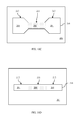
- the methods begin with a substrate 201 (see process 102 and FIG. 2 ).
- the substrate 201 can be a bulk semiconductor substrate, as illustrated.
- the bulk semiconductor substrate can, for example, be made of a first semiconductor material (e.g., silicon).
- the bulk semiconductor substrate can optionally include ground plane doping in the form of well region(s) (not shown) in order to prevent through-substrate leakage from subsequently formed devices thereon.
- the substrate 201 can be a semiconductor-on-insulator substrate, which includes a semiconductor substrate, an insulator layer on the semiconductor substrate and a semiconductor layer on the insulator layer.
- the substrate 201 can be a silicon-on-insulator (SOI) substrate, which includes a silicon substrate, a silicon dioxide (SiO 2 ) insulator layer on the silicon substrate and a silicon layer on the insulator layer.
- SOI silicon-on-insulator
- NSs Stacked elongated nanoshapes
- NWs nanowires
- nanosheets or nanofins can be formed above the substrate 201 such that all of the NSs are made of the first semiconductor material (e.g., silicon) (see process 104 ).
- first semiconductor material e.g., silicon
- alternating layers 202 of a sacrificial material 203 and the first semiconductor material 204 can be formed on the top surface of the substrate 201 (see process 106 and FIG. 2 ). For purposes of illustration, four alternating layers 202 including two layers of the sacrificial material 203 and two layers of the first semiconductor material 204 are shown.
- the first semiconductor material 204 can, for example, be silicon.
- the sacrificial material 203 can be any suitable sacrificial material that is different from the first semiconductor material 204 and can be selectively etched over that first semiconductor material 204 .
- the sacrificial material 203 can be a sacrificial semiconductor material and, particularly, a different semiconductor material from the first semiconductor material 204 , such as silicon germanium, silicon carbide, etc.
- the sacrificial material could be a sacrificial dielectric material.
- the lower layer(s) of the first semiconductor material 204 and upper layer(s) of the first semiconductor material 204 within the alternating layers 202 can be doped so as to different type conductivities to ensure that lower NS(s) and upper NS(s), which will be formed using portions of the layers of the first semiconductor material 204 will have different type conductivities, respectively.
- the upper layer(s) of the first semiconductor material 204 can be doped so as to have a first-type conductivity at a relatively low conductivity (e.g., N ⁇ conductivity) and the lower layer(s) of the first semiconductor material 204 can be doped so as to have a second-type conductivity at a relatively low conductivity level (e.g., P ⁇ conductivity).
- the first semiconductor material 204 within the alternating layers 202 can remain undoped.
- the alternating layers 202 can subsequently be patterned to form a multi-layer semiconductor body 210 on the substrate 201 (see process 108 and FIGS. 3A-3D ). Specifically, lithographic patterning and etch processes (or any other suitable patterning and etch processes) can be performed in order to pattern the alternating layers 202 into a multi-layer semiconductor body 210 .
- This multi-layer semiconductor body 210 can have a first portion 211 with a first width 213 a and can further having second portions 212 with a second width 213 b .
- the first portion 211 can be positioned laterally between the second portions 212 .
- FIG. 3C is an exemplary top view of the partially completed structure shown in FIGS.
- FIG. 3D is an alternative exemplary top view of the partially completed structure shown in FIGS. 3A-3B illustrating that the multi-layer semiconductor body 210 can be a multi-layer semiconductor fin (i.e., a relatively thin, elongated, essentially rectangular-shaped semiconductor body), wherein the first width 213 a of the first portion 211 is approximately equal to the second width 213 b of the second portions 212 .
- the first portion 211 can be patterned into multiple parallel sections positioned side-by side and extending laterally between the second portions 212 (not shown).
- each layer of the first semiconductor material 204 within the first portion 211 of the multi-layer semiconductor body 210 will subsequently be made into an elongated nanoshape (NS) (as defined above)
- the thickness of each layer of the first semiconductor material 204 and/or the first width 213 a of the first portion 211 of the multi-layer semiconductor body 210 should be constrained to tens of nanometers or less (i.e., constrained to 100 nm or less), as discussed in detail above.
- a mask 215 can be formed over the multi-layer semiconductor body 210 and patterned so as to have discrete sections, which cover and protect the top surfaces and sidewalls of the second portions 212 of the multi-layer semiconductor body 210 , and an opening 216 , which is positioned laterally between the sections and which exposes the top surface and sidewalls of the first portion 211 of the multi-layer semiconductor body 210 (see process 110 and FIGS. 4A-4C ).
- a hardmask layer such as a silicon nitride hardmask layer can be deposited over the multi-layer semiconductor body 210 . Lithographic patterning and etch processes can subsequently be performed in order to form the mask 215 with the opening 216 which exposes the top surface and sidewalls of the first portion 211 of the multi-layer semiconductor body 210 .
- exposed sections of the sacrificial material 203 can be selectively removed from the first portion of the multi-layer semiconductor body 210 (see process 112 and FIGS. 5A-5B ).
- an isotropic selective etch process can be performed in order to selectively etch the sacrificial material 203 over the first semiconductor material 204 and the mask 215 .
- a selective etch process is an etch processes wherein one material is selectively etched and, more particularly, etched at a significantly faster rate than one or more other materials so as to remove that one material without significantly impacting the other material(s).
- the silicon germanium can be selectively etched using any of the following exemplary processes: a thermal etch process (e.g., using gaseous hydrochloric acid (HCl)), a dry plasma etch process, or wet etch process with process specifications designed to ensure the selective etch of silicon germanium over silicon and silicon nitride.
- a thermal etch process e.g., using gaseous hydrochloric acid (HCl)
- HCl gaseous hydrochloric acid
- wet etch process with process specifications designed to ensure the selective etch of silicon germanium over silicon and silicon nitride.
- any other suitable isotropic selective etch process could be used.
- this process 112 results in the creation of multiple stacked elongated NSs all made of the first semiconductor material 204 .
- the elongated NSs are shown as NWs. However, it should be understood that, alternatively, these elongated NSs could be nanosheets or nanofins, as described above.
- the number of stacked elongated NSs will depend upon the number of alternating layers 202 of the sacrificial material 203 and the first semiconductor material 204 formed at process 106 above. For example, four alternating layers will result in two elongated NSs, as shown. However, six alternating layers will result in three elongated NSs, eight alternating layers 202 will result in four elongated NSs, and so on. In any case, the stacked NSs will be oriented parallel to the top surface of the substrate 201 , will be stacked one above the other, and will be physically separated from each other.
- the stacked elongated NSs will include at least a lower NS (referred to herein as a first NS 221 ) adjacent to and physically separated from the top surface of the substrate 201 and an upper NS (referred to herein as a second NS 222 ) that is above the first NS(s) 221 (i.e., that is essentially parallel to and physically separated from the first NS 221 such that the first NS is between the second NS 222 and the top surface of the substrate).
- a lower NS referred to herein as a first NS 221
- an upper NS referred to herein as a second NS 222
- the stacked elongated NSs can include multiple lower NSs (i.e., multiple firsts NS 221 ) that are stacked one above the other and/or more than multiple upper NSs (i.e., multiple second NSs 222 ) above the first NS(s) 221 and stacked one above the other.
- the multi-layer semiconductor body 210 is patterned such that the first portion 211 has multiple parallel sections positioned side-by-side and extending laterally between the second portions 212 , the process 112 of removing exposed sections of the sacrificial material from the first portion 211 will result in multiple, parallel, essentially identical, stacks of elongated NSs that are positioned side-by-side (not shown).
- the first NS(s) 221 can have a first-type conductivity at a relatively low conductivity (e.g., N ⁇ conductivity) and the second NS(s) 221 can have a second-type conductivity at a relatively low conductivity level (e.g., P ⁇ conductivity).
- the first NS(s) 221 and the second NS(s) 222 can be undoped.
- the second NS(s) 222 can be selectively processed in order to convert the second NS(s) 222 from the first semiconductor material 204 to a second semiconductor material that is different from the first semiconductor material 204 (see process 114 ).
- a dielectric layer 217 can be deposited so as to fill the opening 216 , optionally polished (e.g., using a chemical mechanical polishing (CMP) process to expose the top surface of the mask 215 , and then recessed to expose the second NS(s) 222 (see processes 116 - 118 and FIGS. 6A-6B ).
- CMP chemical mechanical polishing
- the dielectric layer 217 deposited at process 116 can specifically be made of a different material than the mask 215 .
- the dielectric layer 217 can be made of silicon dioxide, silicon oxycarbide, silicon carbon nitride, silicon boron carbon, or some other dielectric material that can be selectively etch over the first semiconductor material 204 of the elongated NSs 221 / 222 and the mask 215 .
- This dielectric layer 217 can then be recessed at process 118 using a selective etch process to a level below the second NS(s) 222 and above the first NS(s) 221 .
- a third semiconductor material 205 can be conformally deposited on the second NS(s) 222 (see process 120 and FIGS. 7A-7B ).
- the third semiconductor material 205 can be epitaxially grown on exposed surfaces of the second NS(s) 222 so as to wrap completely around each of the second NS(s) 222 individually.
- the third semiconductor material 205 can be, for example, germanium.
- a thermal anneal process can be performed in order to covert the second NS(s) 222 from the first semiconductor material 204 to a second semiconductor material 206 , which is an alloy of the first semiconductor material 204 and the third semiconductor material 205 (see process 122 and FIGS. 8A-8B ).
- the thermal anneal process will result in a second semiconductor material 206 and, particularly, silicon germanium.
- Exemplary thermal anneal processes that can be used to covert silicon and germanium into silicon germanium at process 112 include one or two-step germanium condensation processes performed at temperature ranges of 900° C. to 1200° C. for 10 seconds up to 10 minutes in an ambient atmosphere or a nitrogen (N 2 ) atmosphere. It should be understood that the volume of germanium deposited onto a silicon NS as compared to the volume of the silicon NS itself will determined the ratio of germanium to silicon in the resulting silicon germanium alloy NS.
- the result will be second NS(s) 222 made of an alloy of 50% germanium and 50% silicon. If, however, a lesser volume or a greater volume of germanium is deposited, then the result will be second NS(s) 222 made of an alloy having a greater or lesser ratio of germanium to silicon, respectively. In any case, the preferred thickness of the germanium layer would range from 2 to 5 nms.
- the dielectric layer 217 can be recessed to expose the first NS(s) 221 (see process 124 and FIGS. 9A-9B ). That is, the dielectric layer 217 can be selectively etched over the second semiconductor material 206 of the second NS(s) 222 , the first semiconductor material 204 of the first NS(s) 221 and the mask 215 in order to recess the dielectric layer 217 to a level below the first NS(s) 221 and above the top surface of the substrate 201 . Following recessing of the dielectric layer 217 , the mask 215 can be selectively removed (see process 126 and FIGS. 10A-10B and either FIG. 10C or 10D ).
- FIGS. 10A-10B are cross-section illustrations of the resulting semiconductor structure 200 and FIGS. 10C and 10D are alternative top view illustrations of the same semiconductor structure 200 ,
- this semiconductor structure 200 can include a substrate 201 .
- the substrate 201 can be a bulk semiconductor substrate, as illustrated, with optional ground plane doping in the form of well region(s) (not shown) in order to prevent through-substrate leakage from devices formed thereon.
- the substrate 201 can be a semiconductor layer (e.g., a silicon layer) of a semiconductor-on-insulator substrate (e.g., a silicon-on-insulator (SOI) substrate).
- SOI silicon-on-insulator
- the semiconductor structure 200 can further include a semiconductor body 210 .
- the semiconductor body 210 can have a first portion 211 and second portions 212 , wherein the first portion 211 is positioned laterally between the second portions 212 .
- the first portion 211 can have a first width 213 a and the second portions 212 can have a second width 213 b .
- the first width 213 a can be less than the second width 213 b .
- the first width 213 a can be approximately equal to the second width 213 b.
- the first portion 211 can include stacked elongated nanoshapes (NSs) 221 / 222 (e.g., nanowires (NWs), nanosheets or nanofins), which are above the substrate 201 and which extend laterally between the second portions 212 .
- NSs nanoshapes
- These stacked NSs 221 / 222 can be oriented parallel to the top surface of the substrate 201 , can be stacked one above the other, and can be physically separated from each other.
- the stacked NSs can include one or more lower NSs (referred to herein as first NS(s) 221 ), which are made of a first semiconductor material 204 , and one or more upper NSs (referred to herein as second NS(s) 222 ), which are above the first NS(s) 221 and which are made of a second semiconductor material 206 that is different from the first semiconductor material 204 .
- first semiconductor material 204 of the first NS(s) 221 can be silicon and the second semiconductor material 206 of the second NS(s) 222 can be silicon germanium.
- each NS 221 / 222 and the width of each NS 221 / 222 (which corresponds to the first width 213 a ) can be constrained to tens of nanometers or less (i.e., constrained to 100 nm or less), as discussed in detail above.
- the semiconductor structure 200 of FIGS. 10A-10B and FIG. 10C or FIG. 10D can be used to form multiple stacked devices.
- the first NS(s) 221 and the second NS(s) 222 can be used to form one or more stacked first devices 251 and one or more stacked second devices 252 , respectively, wherein the second device(s) 252 is/are stacked above the first device(s) 251 such that the first device(s) 251 are positioned between the second device(s) 252 and the top surface of the substrate 201 (see process 128 ).
- the semiconductor structure 200 can be further processed in order to form an additional semiconductor structure 260 , which includes at least one first field effect transistor (FET) 251 (e.g., an N-type FET) that incorporates one or more of the first NS(s) 221 as channel region(s) and at least one second FET 252 (e.g., a P-type FET) that incorporates one or more of the second NS(s) 222 as channel region(s), wherein the FET devices are stacked with the second FET(s) 252 being above the first FET(s) 251 such that the first FET(s) 251 are between the second FET(s) 252 and the top surface of the substrate 201 (see FIGS. 11A-11B ).
- FET field effect transistor
- a sacrificial gate structure having a sacrificial gate cap, can be formed adjacent to the first portion 211 of the semiconductor body 210 such that it wraps around the first NS(s) 221 and the second NS(s) 222 .
- a gate sidewall spacer 239 can be formed adjacent to the sacrificial gate structure.
- Source/drain recesses can be formed in the second portions 212 of the semiconductor body 210 on opposing sides of the sacrificial gate structure. The source/drain recesses can, for example, extend to or partially into the substrate 201 . Alternatively, the source/drain recesses can extend to or into the lowest layer of the sacrificial material 203 within the second portions 212 .
- first source/drain regions 241 with a first-type conductivity at a relatively high conductivity level can be formed (e.g., by epitaxial deposition and in-situ doping) in lower portions of the source/drain recesses such that the first NS(s) 221 is/are positioned laterally between the first source/drain regions 241 .
- a relatively high conductivity level e.g., N+ conductivity
- Second source/drain regions 242 with a second-type conductivity at a relatively high conductivity level can be formed (e.g., by epitaxial deposition and in-situ doping) in upper portions of the source/drain recesses above the first source/drain regions 241 such that the second NS(s) 222 is/are positioned laterally between the second source/drain regions 242 .
- the epitaxial semiconductor material used for the first source/drain regions 241 and the second source/drain regions 242 can be the same semiconductor material (e.g., silicon), which is simply in-situ doped so as to have the different type conductivities.
- the epitaxial semiconductor materials used for the first source/drain regions 241 and the second source/drain regions 242 can be different semiconductor materials, which are pre-selected to provide optimal mobility in the NWFET channel regions.
- isolation region(s) 243 e.g., a dielectric isolation region, such as a silicon dioxide isolation region; etc.
- first source/drain regions 241 can be formed on one or both of the first source/drain regions 241 to provide electrical isolation between adjacent first and second source/drain regions.
- processes should be performed to prevent isolation material from forming on exposed vertical surface(s) of the second NS(s) 222 and/or to remove isolation material that has formed on the exposed vertical surface(s) of the second NS(s) prior to formation of the second source/drain regions 242 .
- isolation region(s) 243 are formed above first source/drain region(s) 241
- the second source/drain region(s) 242 can be formed above the isolation region(s) 243 by lateral epitaxial deposition on the exposed vertical surface(s) of the second NS(s) 222 .
- interlayer dielectric (ILD) material 245 can be deposited.
- the ILD material 245 can be, for example, silicon dioxide or some other suitable ILD material (e.g., borophosphosilicate glass (BPSG), tetraethyl orthosilicate (TEOS), fluorinated tetraethyl orthosilicate (FTEOS), etc.).
- BPSG borophosphosilicate glass
- TEOS tetraethyl orthosilicate
- FTEOS fluorinated tetraethyl orthosilicate
- the ILD material 245 can subsequently be polished (e.g., using a CMP process) to expose the top surface of the sacrificial gate structure and the sacrificial gate structure can be selectively removed, thereby creating a second opening (i.e., a gate opening) that is bounded by the gate sidewall spacer 239 and that exposes the stacked elongated NSs including the lower NS(s) (i.e., the first NS(s) 221 ) and the upper NS(s) (i.e., the second NS(s) 222 ).
- a second opening i.e., a gate opening
- a first replacement metal gate (RMG) structure 231 having a first work function
- a second RMG structure 232 having a second work function that is different from the first work function
- Exemplary processes that can be used to form the RMGs 231 / 232 can include conformally depositing a gate dielectric layer into the second opening such that it lines the second opening and wraps around each elongated NS 221 / 222 .
- a first work function metal layer 234 for the first RMG 231 can be deposited onto the gate dielectric layer and etched back so that it wraps around the first NS(s) 221 but not the second NS(s) 222 .
- the first work function metal layer 234 can be a conformal work function metal layer and a conductive fill material (not shown) can be deposited and recessed so that it fills remaining space within the lower portion of the second opening below the level of the second NS(s) 222 .
- a second work function metal layer 235 for the second RMG 232 can be deposited in the upper portion of the second opening such that it wraps around the second NS(s) 222 .
- the second work function metal layer 235 can be a conformal work function metal layer and a conductive fill material (not shown) can be deposited to fill any remaining space within the upper portion of the second opening.
- the second RMG 232 can then be recessed slightly to enable formation of a dielectric gate cap 236 within the second opening above the second RMG 232 .
- a dielectric gate cap layer can be deposited into a recess formed above the second RMG 232 and a polishing process (e.g., a CMP process) can be performed in order to remove the dielectric gate cap material from above the ILD material 245 , thereby forming the dielectric gate cap 236 .
- an isolation region 233 e.g., a dielectric isolation region, such as a silicon dioxide isolation region
- a dielectric isolation region such as a silicon dioxide isolation region
- the exemplary method embodiment described above uses replacement metal gate (RMG) processing to form the first RMG 231 of the first FET 251 and the second RMG 232 of the second FET 252 .
- RMG replacement metal gate
- this description is not intended to be limiting and that, alternatively, gate-first gate processing could be used to form the first gate structure 231 and the second gate structure 232 .
- Additional processing can then be performed in order to complete the semiconductor structure 260 , which includes the first FET 251 and the second FET 252 stacked above the first FET 251 .
- the additional processing can include, but is not limited to, the formation of middle of the line (MOL) contacts to the gate structures 231 / 232 and to the source/drain regions 241 / 242 and back end of the line (BEOL) processes.
- MOL middle of the line
- BEOL back end of the line
- an isolation region 233 is formed between the first and second RMGs 231 / 232 or if isolation region(s) 243 are formed between adjacent first and second source/drain regions 241 / 242 , processes should be performed in order to ensure that the MOL contacts to the lower RMG (i.e., to the first RMG 231 ) and to the lower source/drain region(s) (i.e., to the first source/drain region(s) 241 ) are electrically isolated from the upper RMG (i.e., the second RMG 232 ) and from the upper source/drain region(s) (i.e., the second source/drain region(s) 242 ).
- These processes can include, for example, ensuring that the first RMG 231 extends laterally beyond the second RMG 232 so that the contact to the first RMG 231 can extend vertically through dielectric material and land on the first RMG 231 without contacting the second RMG 232 .
- These processes can also include, for example, ensuring that the first source/drain regions 241 extends laterally beyond the second source/drain regions 242 so that the contacts to the first source/drain regions 241 can extend vertically through dielectric material and land on the first source/drain regions 241 without contacting the second source/drain regions 242 .
- these processes can include the formation of the MOL contacts to the first RMG 231 and the first source/drain regions 241 such that the sidewalls of these contacts are lined with isolation material.
- this method is described above and illustrated in the figures with respect to the formation of only a single first FET 251 that incorporates a single first NS 221 and, stacked above the first FET 251 , a single second FET 252 that incorporates a single second NS 222 .
- additional embodiments of the method could include any of the following: (a) the formation of a single first FET 251 that incorporates multiple first NSs 221 , which are stacked and/or side-by-side, as channel regions and, stacked above the first FET 251 , a single second FET 252 that incorporates a single second NS 222 as a channel region; (b) the formation of a single first FET 251 that incorporates a single first NS 221 as a channel region and, stacked above the first FET 251 , a single second FET 252 that incorporates multiple second NSs 222 , which are stacked and/or side-by-side, as channel regions; (c) the formation of a single first FET 251 that incorporates multiple first NSs 221 , which are stacked and/or side-by-side, as channel regions and, stacked above the first FET 251 , a single second FET 252 that incorporates multiple second NSs
- stacked FETs with the same type conductivity can share a gate structure and/or source/drain regions or can have discrete gate structures (e.g., electrically isolated by isolation regions) and/or discrete source/drain regions (e.g., electrically isolated by isolation regions).
- the resulting semiconductor structure 260 of FIGS. 11A-11B can include a substrate 201 .
- the substrate 201 can be a bulk semiconductor substrate, as illustrated, with optional ground plane doping in the form of well region(s) (not shown) in order to prevent through-substrate leakage from devices formed thereon.
- the substrate 201 can be a semiconductor layer (e.g., a silicon layer) of a semiconductor-on-insulator substrate (e.g., a silicon-on-insulator (SOI) substrate).
- SOI silicon-on-insulator
- the semiconductor structure 260 can further include, above a top surface of the substrate, at least one first field effect transistor (FET) 251 , which has has a first-type conductivity (e.g., an N-type FET) and which incorporates one or more first nanoshapes (NSs) 221 as channel region(s).
- FET field effect transistor
- the semiconductor structure 260 can further include at least one second FET 252 , which has a second-type conductivity (e.g., a P-type NWFET) and which incorporates one or more second NS(s) 222 as channel region(s).
- the FETs 251 / 522 can be arranged in a stack one above the other with the second FET(s) 252 being above the first FET(s) 251 such that the first FET(s) 251 are between the second FET(s) 252 and the top surface of the substrate 201 .
- the semiconductor structure 260 can include stacked elongated nanoshapes (NSs) 221 / 222 that are oriented parallel to the top surface of the substrate 201 , that are stacked one above the other, and that are physically separated from each other.
- the stacked elongated NSs can include one or more lower NSs (referred to herein as first NS(s) 221 , as discussed in detail above with regard to the methods), which are either undoped or have the second-type conductivity at a relatively low conductivity level (e.g., P ⁇ conductivity), which function as first channel region(s) for the first FET(s) 251 and which are made of a first semiconductor material 204 .
- the stacked elongated NSs can also include one or more upper NSs (referred to herein as second NS(s) 222 , as discussed in detail above with regard to the methods), which function as second channel region(s) for the second FET(s) 252 , which are above the first NS(s) 221 , and which are made of a second semiconductor material 206 that is different from the first semiconductor material 204 .
- the first semiconductor material 204 can be, for example, silicon and the second semiconductor material 206 can be, for example, silicon germanium.
- These stacked elongated NSs can be nanowires (NWs), nanosheets or nanofins.
- each elongated NS 221 / 222 and/or the width (also referred to as the depth) of each elongated NS 221 / 222 can be constrained to tens of nanometers or less (i.e., constrained to 100 nm or less), as discussed in detail above.
- the first FET 251 can further include first source/drain regions 241 and one or more first NS(s) 221 (i.e., first channel region(s)) that can extend laterally between the first source/drain regions 241 .
- the first FET 251 can further include a first gate structure 231 (e.g., a first replacement metal gate (RMG) structure), which has a first work function and which is wrapped around the first NS(s) 221 .
- RMG replacement metal gate
- the first FET 251 can have the first-type conductivity (e.g., N-type conductivity).
- the first source/drain regions 241 can have the first-type conductivity at a relatively high conductivity level (e.g., N+ conductivity).
- the second FET 252 can further include second source/drain regions 242 .
- the second source/drain regions 242 can be above the first source/drain regions 241 and one or more second NS(s) 222 (i.e., second channel region(s)) can be positioned laterally between the second source/drain regions 242 .
- the second FET 252 can further include a second gate structure 232 (e.g., a second replacement metal gate (RMG) structure) above the first gate structure 231 and wrapped around the second NS(s) 222 .
- the second FET 252 can have the first-type conductivity (e.g., P-type conductivity).
- the second source/drain regions 242 can have the second-type conductivity at a relatively high conductivity level (e.g., P+ conductivity).
- the semiconductor structure 260 can further include any of the following: an isolation region 233 electrically isolating the first gate structure 231 from the second gate structure 232 and/or one or more additional isolation regions 243 , wherein each isolation region 243 electrically isolates a first source/drain region 241 from the second source/drain region 242 above.
- the stacked first FETs can share the same first gate structure or can have discrete first gate structures (e.g., electrically isolated by isolation regions) and/or can share first source/drain regions or can have discrete first source/drain regions (e.g., electrically isolated by isolation regions).
- the stacked second FETs can share the same second gate structure or can have discrete second gate structures (e.g., electrically isolated by isolation regions) and/or can share second source/drain regions or can have discrete second source/drain regions (e.g., electrically isolated by isolation regions).
- the disclosed methods result in semiconductor structures 200 and 260 that consume less of the available surface area of the substrate and, thereby allow for further size scaling.
- the first FET 251 has the first-type conductivity (e.g., is an N-type FET) and the second FET 252 has a second-type conductivity (e.g., is a P-type FET).
- the channel region(s) can have P-type conductivity at a relatively low conductivity level (or can be undoped) and the source/drain regions can have N-type conductivity and a relatively high conductivity level; whereas, for a P-type FET, the channel region(s) can have N-type conductivity at a relatively low conductivity level (or can be undoped) and the source/drain regions can have P-type conductivity at a relatively high conductivity level.
- different dopants can be used to achieve the different conductivity types and that the dopants may vary depending upon the different semiconductor materials used.
- a silicon-based semiconductor material e.g., silicon, silicon germanium, etc.
- N-type dopant e.g., a Group V dopant, such as arsenic (As), phosphorous (P) or antimony (Sb)
- P-type dopant e.g., a Group III dopant, such as boron (B) or indium (In)
- GaN gallium nitride
- Si silicon
- the first FET 251 can have a first gate structure 231 with a first work function and the second FET 252 can have a second gate structure 232 with a second work function.
- the gate dielectric layer can be a silicon dioxide gate dielectric layer.
- the gate dielectric layer can be a high-K gate dielectric layer.
- the high-K gate dielectric layer can be, for example, a dielectric material with a dielectric constant that is greater than the dielectric constant of silicon dioxide (i.e., greater than 3.9).
- Exemplary high-K dielectric materials include, but are not limited to, hafnium (Hf)-based dielectrics (e.g., hafnium oxide, hafnium silicon oxide, hafnium silicon oxynitride, hafnium aluminum oxide, etc.) or other suitable high-k dielectrics (e.g., aluminum oxide, tantalum oxide, zirconium oxide, etc.).
- the work function metal of the RMG can include a metal material or metal alloy material that is preselected in order to achieve the optimal gate conductor work function given the conductivity type of the FET.
- the optimal gate conductor work function of the N-type FET 251 will be, for example, between 3.9 eV and about 4.2 eV.
- Exemplary metals (and metal alloys) having a work function within this range include, but are not limited to, hafnium, zirconium, titanium, tantalum, aluminum, and alloys thereof, such as, hafnium carbide, zirconium carbide, titanium carbide, tantalum carbide, and aluminum carbide.
- the optimal gate conductor work function for the P-type FET 252 will be, for example, between about 4.9 eV and about 5.2 eV.
- Exemplary metals (and metal alloys) having a work function within this range include, but are not limited to, ruthenium, palladium, platinum, cobalt, and nickel, as well as metal oxides (aluminum carbon oxide, aluminum titanium carbon oxide, etc.) and metal nitrides (e.g., titanium nitride, titanium silicon nitride, tantalum silicon nitride, titanium aluminum nitride, tantalum aluminum nitride, etc.).
- Any conductive fill material used can be a fill metal or fill metal alloy, such as tungsten, a tungsten alloy (e.g., tungsten silicide or titanium tungsten), cobalt, aluminum or any other suitable fill metal or fill metal alloy.
- laterally is used herein to describe the relative locations of elements and, more particularly, to indicate that an element is positioned to the side of another element as opposed to above or below the other element, as those elements are oriented and illustrated in the drawings.
- an element that is positioned laterally adjacent to another element will be beside the other element
- an element that is positioned laterally immediately adjacent to another element will be directly beside the other element
- an element that laterally surrounds another element will be adjacent to and border the outer sidewalls of the other element.
- stacked elongated nanoshapes e.g., nanowires (NWs)
- NWs nanowires
- stacked devices e.g., stacked field effect transistors (FETs) with different type conductivities for complementary metal oxide semiconductor (CMOS) circuitry
- FETs stacked field effect transistors
- CMOS complementary metal oxide semiconductor
- stacked elongated NSs made of the same first semiconductor material can be formed above a substrate.
- the stacked elongated NSs can include at least a first NS and a second NS above the first NS.
- the second NS can then be selectively processed in order to convert the second NS from the first semiconductor material to a second semiconductor material.
- the first and second NSs can subsequently be used to form first and second devices, respectively, wherein the second device is stacked above the first device.
- the first and second devices can be, for example, first and second FETs, respectively, having different type conductivities.
Landscapes
- Engineering & Computer Science (AREA)
- Chemical & Material Sciences (AREA)
- Nanotechnology (AREA)
- Physics & Mathematics (AREA)
- Theoretical Computer Science (AREA)
- Crystallography & Structural Chemistry (AREA)
- Mathematical Physics (AREA)
- Condensed Matter Physics & Semiconductors (AREA)
- General Physics & Mathematics (AREA)
- Manufacturing & Machinery (AREA)
- Computer Hardware Design (AREA)
- Microelectronics & Electronic Packaging (AREA)
- Power Engineering (AREA)
- Metal-Oxide And Bipolar Metal-Oxide Semiconductor Integrated Circuits (AREA)
- Thin Film Transistor (AREA)
Abstract
Description
Claims (18)
Priority Applications (3)
| Application Number | Priority Date | Filing Date | Title |
|---|---|---|---|
| US15/629,884 US10453750B2 (en) | 2017-06-22 | 2017-06-22 | Stacked elongated nanoshapes of different semiconductor materials and structures that incorporate the nanoshapes |
| TW106145999A TWI705040B (en) | 2017-06-22 | 2017-12-27 | Stacked elongated nanoshapes of different semiconductor materials, structures that incorporate the nanoshapes and methods of forming the same |
| CN201810239670.7A CN109119340B (en) | 2017-06-22 | 2018-03-22 | Stacked strip nano-shape composed of different semiconductor materials and structure thereof |
Applications Claiming Priority (1)
| Application Number | Priority Date | Filing Date | Title |
|---|---|---|---|
| US15/629,884 US10453750B2 (en) | 2017-06-22 | 2017-06-22 | Stacked elongated nanoshapes of different semiconductor materials and structures that incorporate the nanoshapes |
Publications (2)
| Publication Number | Publication Date |
|---|---|
| US20180374753A1 US20180374753A1 (en) | 2018-12-27 |
| US10453750B2 true US10453750B2 (en) | 2019-10-22 |
Family
ID=64692734
Family Applications (1)
| Application Number | Title | Priority Date | Filing Date |
|---|---|---|---|
| US15/629,884 Active US10453750B2 (en) | 2017-06-22 | 2017-06-22 | Stacked elongated nanoshapes of different semiconductor materials and structures that incorporate the nanoshapes |
Country Status (3)
| Country | Link |
|---|---|
| US (1) | US10453750B2 (en) |
| CN (1) | CN109119340B (en) |
| TW (1) | TWI705040B (en) |
Cited By (3)
| Publication number | Priority date | Publication date | Assignee | Title |
|---|---|---|---|---|
| US11183574B2 (en) | 2019-05-24 | 2021-11-23 | Taiwan Semiconductor Manufacturing Co., Ltd. | Work function layers for transistor gate electrodes |
| US11315938B1 (en) | 2020-12-18 | 2022-04-26 | International Business Machines Corporation | Stacked nanosheet rom |
| US11973082B2 (en) | 2020-12-24 | 2024-04-30 | Samsung Electronics Co., Ltd. | Integrated circuit devices |
Families Citing this family (13)
| Publication number | Priority date | Publication date | Assignee | Title |
|---|---|---|---|---|
| US10381438B2 (en) * | 2017-11-02 | 2019-08-13 | International Business Machines Corporation | Vertically stacked NFETS and PFETS with gate-all-around structure |
| US11335807B2 (en) * | 2018-06-29 | 2022-05-17 | Intel Corporation | Isolation schemes for gate-all-around transistor devices |
| US10510622B1 (en) | 2018-07-27 | 2019-12-17 | Globalfoundries Inc. | Vertically stacked complementary-FET device with independent gate control |
| US10916629B2 (en) * | 2018-07-31 | 2021-02-09 | International Business Machines Corporation | Nanosheet-CMOS EPROM device with epitaxial oxide charge storage region |
| US10892328B2 (en) * | 2019-03-04 | 2021-01-12 | International Business Machines Corporation | Source/drain extension regions and air spacers for nanosheet field-effect transistor structures |
| US11676966B2 (en) | 2019-03-15 | 2023-06-13 | Intel Corporation | Stacked transistors having device strata with different channel widths |
| DE102020106252A1 (en) | 2019-04-12 | 2020-10-15 | Taiwan Semiconductor Manufacturing Co., Ltd. | INTEGRATED CIRCUIT |
| US10971630B2 (en) * | 2019-04-24 | 2021-04-06 | Taiwan Semiconductor Manufacturing Co., Ltd. | Semiconductor structure having both gate-all-around devices and planar devices |
| US11769836B2 (en) * | 2019-05-07 | 2023-09-26 | Intel Corporation | Gate-all-around integrated circuit structures having nanowires with tight vertical spacing |
| US11296199B2 (en) * | 2019-10-29 | 2022-04-05 | Taiwan Semiconductor Manufacturing Company, Ltd. | Semiconductor devices and methods |
| US11621197B2 (en) | 2021-02-15 | 2023-04-04 | Taiwan Semiconductor Manufacturing Company, Ltd. | Semiconductor device with gate cut feature and method for forming the same |
| US12176345B2 (en) | 2021-09-23 | 2024-12-24 | International Business Machines Corporation | Stacked FET with independent gate control |
| US20240355929A1 (en) * | 2023-04-19 | 2024-10-24 | Applied Materials, Inc. | Dual gate structure for memory device |
Citations (13)
| Publication number | Priority date | Publication date | Assignee | Title |
|---|---|---|---|---|
| US20030139000A1 (en) | 2002-01-23 | 2003-07-24 | International Business Machines Corporation | Method of creating high-quality relaxed SiGe-on-insulator for strained Si CMOS applications |
| TW200616051A (en) | 2004-09-14 | 2006-05-16 | Ibm | Structure and method for enhanced uni-directional diffusion of cobalt silicide |
| US20080135949A1 (en) | 2006-12-08 | 2008-06-12 | Agency For Science, Technology And Research | Stacked silicon-germanium nanowire structure and method of forming the same |
| TW200826161A (en) | 2006-12-13 | 2008-06-16 | Siltronic Ag | Verfahren zur herstellung von SGOI-und GeOI-halbleiterstrukturen |
| TWI304622B (en) | 2003-09-03 | 2008-12-21 | Ibm | Use of thin soi to inhibit relaxation of sige layers |
| US7601570B2 (en) | 2006-08-25 | 2009-10-13 | Commissariat A L'energie Atomique | Method for producing a device comprising a structure equipped with one or more microwires or nanowires based on a Si and Ge compound by germanium condensation |
| US8173993B2 (en) | 2009-12-04 | 2012-05-08 | International Business Machines Corporation | Gate-all-around nanowire tunnel field effect transistors |
| US8679902B1 (en) | 2012-09-27 | 2014-03-25 | International Business Machines Corporation | Stacked nanowire field effect transistor |
| US9425293B1 (en) * | 2015-12-30 | 2016-08-23 | International Business Machines Corporation | Stacked nanowires with multi-threshold voltage solution for pFETs |
| US9437501B1 (en) | 2015-09-22 | 2016-09-06 | International Business Machines Corporation | Stacked nanowire device width adjustment by gas cluster ion beam (GCIB) |
| US20170005190A1 (en) | 2015-06-30 | 2017-01-05 | International Business Machines Corporation | Local germanium condensation for suspended nanowire and finfet devices |
| US20170077232A1 (en) | 2015-09-11 | 2017-03-16 | International Business Machines Corporation | STRAINED STACKED NANOWIRE FIELD-EFFECT TRANSISTORS (FETs) |
| US20180277628A1 (en) * | 2017-03-27 | 2018-09-27 | International Business Machines Corporation | Nanosheet cmos transistors |
Family Cites Families (3)
| Publication number | Priority date | Publication date | Assignee | Title |
|---|---|---|---|---|
| KR101824971B1 (en) * | 2011-12-23 | 2018-02-05 | 인텔 코포레이션 | Semiconductor structures having modulated nanowire counts and methods for fabricating the same |
| US9263520B2 (en) * | 2013-10-10 | 2016-02-16 | Globalfoundries Inc. | Facilitating fabricating gate-all-around nanowire field-effect transistors |
| US9502518B2 (en) * | 2014-06-23 | 2016-11-22 | Stmicroelectronics, Inc. | Multi-channel gate-all-around FET |
-
2017
- 2017-06-22 US US15/629,884 patent/US10453750B2/en active Active
- 2017-12-27 TW TW106145999A patent/TWI705040B/en active
-
2018
- 2018-03-22 CN CN201810239670.7A patent/CN109119340B/en active Active
Patent Citations (13)
| Publication number | Priority date | Publication date | Assignee | Title |
|---|---|---|---|---|
| US20030139000A1 (en) | 2002-01-23 | 2003-07-24 | International Business Machines Corporation | Method of creating high-quality relaxed SiGe-on-insulator for strained Si CMOS applications |
| TWI304622B (en) | 2003-09-03 | 2008-12-21 | Ibm | Use of thin soi to inhibit relaxation of sige layers |
| TW200616051A (en) | 2004-09-14 | 2006-05-16 | Ibm | Structure and method for enhanced uni-directional diffusion of cobalt silicide |
| US7601570B2 (en) | 2006-08-25 | 2009-10-13 | Commissariat A L'energie Atomique | Method for producing a device comprising a structure equipped with one or more microwires or nanowires based on a Si and Ge compound by germanium condensation |
| US20080135949A1 (en) | 2006-12-08 | 2008-06-12 | Agency For Science, Technology And Research | Stacked silicon-germanium nanowire structure and method of forming the same |
| TW200826161A (en) | 2006-12-13 | 2008-06-16 | Siltronic Ag | Verfahren zur herstellung von SGOI-und GeOI-halbleiterstrukturen |
| US8173993B2 (en) | 2009-12-04 | 2012-05-08 | International Business Machines Corporation | Gate-all-around nanowire tunnel field effect transistors |
| US8679902B1 (en) | 2012-09-27 | 2014-03-25 | International Business Machines Corporation | Stacked nanowire field effect transistor |
| US20170005190A1 (en) | 2015-06-30 | 2017-01-05 | International Business Machines Corporation | Local germanium condensation for suspended nanowire and finfet devices |
| US20170077232A1 (en) | 2015-09-11 | 2017-03-16 | International Business Machines Corporation | STRAINED STACKED NANOWIRE FIELD-EFFECT TRANSISTORS (FETs) |
| US9437501B1 (en) | 2015-09-22 | 2016-09-06 | International Business Machines Corporation | Stacked nanowire device width adjustment by gas cluster ion beam (GCIB) |
| US9425293B1 (en) * | 2015-12-30 | 2016-08-23 | International Business Machines Corporation | Stacked nanowires with multi-threshold voltage solution for pFETs |
| US20180277628A1 (en) * | 2017-03-27 | 2018-09-27 | International Business Machines Corporation | Nanosheet cmos transistors |
Non-Patent Citations (8)
| Title |
|---|
| Davide Sacchetto et al.,"Vertically-stacked gate-all-around polysilicon nanowire FETs with sub-Im gates patterned by nanostencil lithography", Microelectronic Engineering 98, Jul. 25, 2012, pp. 355-358. |
| Gaillardon et al., "Nanowire systems: technology and design", Phil. Trans. R. Soc. A 372, Jan. 2, 2013, pp. 1-15. |
| Peng Zheng et al., "FinFET Evolution Toward Stacked-Nanowire FET for CMOS Technology Scaling", IEEE.org, Oct. 27, 2015, pp. 1-4. |
| Provided by IMEC, APA citation: "World's first vertically stacked gate-all-around Si nanowire CMOS transistors" (Dec. 23, 2016) retrieved Jun. 14, 2017 from https://phys.org/news/2016-12-world-vertically-stacked-gateall-around-si.html, pp. 1-2. |
| Taiwanese Application No. 106145999, Examination Report dated Feb. 21, 2019 and Search Report dated Feb. 9, 2019, pp. 1-6. |
| Taiwanese Application No. 106145999, Rejection Decision dated Jul. 17, 2019, pp. 1-13. |
| Wilfried Vandervorst et al., "Fabrication of (Silicon)-Germanium on Insulator Substrates by the Germanium Condensation Technique", Katholieke Universiteit Leuven-Faculteit Wetenschap & Technologie Arenbergkasteel, B-3001 Heverlee (Belgie), Apr. 2012, pp. 1-2, and 24-72. |
| Wilfried Vandervorst et al., "Fabrication of (Silicon)-Germanium on Insulator Substrates by the Germanium Condensation Technique", Katholieke Universiteit Leuven—Faculteit Wetenschap & Technologie Arenbergkasteel, B-3001 Heverlee (Belgie), Apr. 2012, pp. 1-2, and 24-72. |
Cited By (5)
| Publication number | Priority date | Publication date | Assignee | Title |
|---|---|---|---|---|
| US11183574B2 (en) | 2019-05-24 | 2021-11-23 | Taiwan Semiconductor Manufacturing Co., Ltd. | Work function layers for transistor gate electrodes |
| US12132091B2 (en) | 2019-05-24 | 2024-10-29 | Taiwan Semiconductor Manufacturing Co., Ltd. | Work function layers for transistor gate electrodes |
| US11315938B1 (en) | 2020-12-18 | 2022-04-26 | International Business Machines Corporation | Stacked nanosheet rom |
| US11973082B2 (en) | 2020-12-24 | 2024-04-30 | Samsung Electronics Co., Ltd. | Integrated circuit devices |
| US12396260B2 (en) | 2020-12-24 | 2025-08-19 | Samsung Electronics Co., Ltd. | Metal-oxide-semiconductor field effect transistors including a plurality of nanosheets |
Also Published As
| Publication number | Publication date |
|---|---|
| TW201904864A (en) | 2019-02-01 |
| US20180374753A1 (en) | 2018-12-27 |
| CN109119340A (en) | 2019-01-01 |
| CN109119340B (en) | 2021-09-10 |
| TWI705040B (en) | 2020-09-21 |
Similar Documents
| Publication | Publication Date | Title |
|---|---|---|
| US10453750B2 (en) | Stacked elongated nanoshapes of different semiconductor materials and structures that incorporate the nanoshapes | |
| US10192819B1 (en) | Integrated circuit structure incorporating stacked field effect transistors | |
| US20230028568A1 (en) | Source/drain contacts for non-planar transistors | |
| US10431663B2 (en) | Method of forming integrated circuit with gate-all-around field effect transistor and the resulting structure | |
| US10580897B2 (en) | Methods of forming a bulk field effect transistor (FET) with sub-source/drain isolation layers and the resulting structures | |
| US10326021B2 (en) | Source/drain profile for FinFeT | |
| US10304832B1 (en) | Integrated circuit structure incorporating stacked field effect transistors and method | |
| CN108878535B (en) | Fin field effect transistor with single diffusion interrupt and method | |
| US10276689B2 (en) | Method of forming a vertical field effect transistor (VFET) and a VFET structure | |
| US10355101B2 (en) | Vertical field effect transistor (VFET) having a self-aligned gate/gate extension structure and method | |
| US10283621B2 (en) | Method of forming vertical field effect transistors with self-aligned gates and gate extensions and the resulting structure | |
| US20190103319A1 (en) | Method of forming vertical field effect transistors with different gate lengths and a resulting structure | |
| US10217846B1 (en) | Vertical field effect transistor formation with critical dimension control | |
| US10014296B1 (en) | Fin-type field effect transistors with single-diffusion breaks and method | |
| US12349410B2 (en) | Nanostructure field-effect transistor (NANO-FET) with gates including a seam in p-type work function metal between nanostructures and methods of forming | |
| US12191393B2 (en) | Low Ge isolated epitaxial layer growth over nano-sheet architecture design for RP reduction | |
| KR101696998B1 (en) | Semiconductor device including a semiconductor sheet unit interconnecting a source and a drain |
Legal Events
| Date | Code | Title | Description |
|---|---|---|---|
| AS | Assignment |
Owner name: GLOBALFOUNDRIES INC., CAYMAN ISLANDS Free format text: ASSIGNMENT OF ASSIGNORS INTEREST;ASSIGNORS:PAWLAK, BARTLOMIEJ J.;BOUCHE, GUILLAUME;JACOB, AJEY P.;REEL/FRAME:042782/0463 Effective date: 20170621 |
|
| STPP | Information on status: patent application and granting procedure in general |
Free format text: RESPONSE TO NON-FINAL OFFICE ACTION ENTERED AND FORWARDED TO EXAMINER |
|
| STPP | Information on status: patent application and granting procedure in general |
Free format text: RESPONSE AFTER FINAL ACTION FORWARDED TO EXAMINER |
|
| STPP | Information on status: patent application and granting procedure in general |
Free format text: NOTICE OF ALLOWANCE MAILED -- APPLICATION RECEIVED IN OFFICE OF PUBLICATIONS |
|
| STPP | Information on status: patent application and granting procedure in general |
Free format text: PUBLICATIONS -- ISSUE FEE PAYMENT RECEIVED |
|
| STCF | Information on status: patent grant |
Free format text: PATENTED CASE |
|
| AS | Assignment |
Owner name: GLOBALFOUNDRIES U.S. INC., CALIFORNIA Free format text: ASSIGNMENT OF ASSIGNORS INTEREST;ASSIGNOR:GLOBALFOUNDRIES INC.;REEL/FRAME:054633/0001 Effective date: 20201022 |
|
| AS | Assignment |
Owner name: GLOBALFOUNDRIES U.S. INC., NEW YORK Free format text: RELEASE BY SECURED PARTY;ASSIGNOR:WILMINGTON TRUST, NATIONAL ASSOCIATION;REEL/FRAME:056987/0001 Effective date: 20201117 Owner name: GLOBALFOUNDRIES U.S. INC., NEW YORK Free format text: RELEASE OF SECURITY INTEREST;ASSIGNOR:WILMINGTON TRUST, NATIONAL ASSOCIATION;REEL/FRAME:056987/0001 Effective date: 20201117 |
|
| MAFP | Maintenance fee payment |
Free format text: PAYMENT OF MAINTENANCE FEE, 4TH YEAR, LARGE ENTITY (ORIGINAL EVENT CODE: M1551); ENTITY STATUS OF PATENT OWNER: LARGE ENTITY Year of fee payment: 4 |