US10446760B2 - Organic compound, organic optoelectric diode, and display device - Google Patents
Organic compound, organic optoelectric diode, and display device Download PDFInfo
- Publication number
- US10446760B2 US10446760B2 US15/117,457 US201515117457A US10446760B2 US 10446760 B2 US10446760 B2 US 10446760B2 US 201515117457 A US201515117457 A US 201515117457A US 10446760 B2 US10446760 B2 US 10446760B2
- Authority
- US
- United States
- Prior art keywords
- group
- unsubstituted
- substituted
- organic
- compound
- Prior art date
- Legal status (The legal status is an assumption and is not a legal conclusion. Google has not performed a legal analysis and makes no representation as to the accuracy of the status listed.)
- Active, expires
Links
- 0 C**CC(C*1CCCC1)I Chemical compound C**CC(C*1CCCC1)I 0.000 description 22
- ZMANZCXQSJIPKH-UHFFFAOYSA-N CCN(CC)CC Chemical compound CCN(CC)CC ZMANZCXQSJIPKH-UHFFFAOYSA-N 0.000 description 3
- GFMQTZBVQABMIQ-UHFFFAOYSA-N C1=CC=C(C2(C3=CC(N(C4=CC5=C(C=C4)C4=C(C=C5)C=CC5=C4OC4=C5C=CC=C4)C4=C5C=CC=CC5=C5C=CC=CC5=C4)=CC=C3)C3=C(C=CC=C3)C3=C2C=CC=C3)C=C1.C1=CC=C(C2(C3=CC(N(C4=CC=C(C5=CC=CC6=C5OC5=C6C=CC=C5)C=C4)C4=CC5=C(C=C4)C4=C(C=C5)C=CC5=C4OC4=C5C=CC=C4)=CC=C3)C3=C(C=CC=C3)C3=C2C=CC=C3)C=C1.C1=CC=C(C2=CC=C(N(C3=CC=C(C4(C5=CC=CC=C5)C5=C(C=CC=C5)C5=C4C=CC=C5)C=C3)C3=CC4=C(C=C3)C3=C(C=C4)C=CC4=C3OC3=C4C=CC=C3)C=C2)C=C1 Chemical compound C1=CC=C(C2(C3=CC(N(C4=CC5=C(C=C4)C4=C(C=C5)C=CC5=C4OC4=C5C=CC=C4)C4=C5C=CC=CC5=C5C=CC=CC5=C4)=CC=C3)C3=C(C=CC=C3)C3=C2C=CC=C3)C=C1.C1=CC=C(C2(C3=CC(N(C4=CC=C(C5=CC=CC6=C5OC5=C6C=CC=C5)C=C4)C4=CC5=C(C=C4)C4=C(C=C5)C=CC5=C4OC4=C5C=CC=C4)=CC=C3)C3=C(C=CC=C3)C3=C2C=CC=C3)C=C1.C1=CC=C(C2=CC=C(N(C3=CC=C(C4(C5=CC=CC=C5)C5=C(C=CC=C5)C5=C4C=CC=C5)C=C3)C3=CC4=C(C=C3)C3=C(C=C4)C=CC4=C3OC3=C4C=CC=C3)C=C2)C=C1 GFMQTZBVQABMIQ-UHFFFAOYSA-N 0.000 description 2
- GCDVCNDXBOYJSF-UHFFFAOYSA-N C1=CC=C(C2(C3=CC(N(C4=CC5=C(C=C4)C4=C(C=C5)C=CC5=C4OC4=C5C=CC=C4)C4=CC5=C(C=C4)C4=C(C=C5)C=CC5=C4OC4=C5C=CC=C4)=CC=C3)C3=C(C=CC=C3)C3=C2C=CC=C3)C=C1.C1=CC=C(C2(C3=CC(N(C4=CC5=C(C=C4)C4=C(C=C5)C=CC5=C4SC4=C5C=CC=C4)C4=CC5=C(C=C4)C4=C(C=C5)C=CC5=C4SC4=C5C=CC=C4)=CC=C3)C3=C(C=CC=C3)C3=C2C=CC=C3)C=C1.C1=CC=C(C2=CC(C3=CC=CC=C3)=CC(N(C3=CC=C4C(=C3)C=CC3=C4C4=C(C=C3)C3=C(C=CC=C3)S4)C3=CC4=C(C=C3)C3=C(C=C4)C=CC4=C3OC3=C4C=CC=C3)=C2)C=C1 Chemical compound C1=CC=C(C2(C3=CC(N(C4=CC5=C(C=C4)C4=C(C=C5)C=CC5=C4OC4=C5C=CC=C4)C4=CC5=C(C=C4)C4=C(C=C5)C=CC5=C4OC4=C5C=CC=C4)=CC=C3)C3=C(C=CC=C3)C3=C2C=CC=C3)C=C1.C1=CC=C(C2(C3=CC(N(C4=CC5=C(C=C4)C4=C(C=C5)C=CC5=C4SC4=C5C=CC=C4)C4=CC5=C(C=C4)C4=C(C=C5)C=CC5=C4SC4=C5C=CC=C4)=CC=C3)C3=C(C=CC=C3)C3=C2C=CC=C3)C=C1.C1=CC=C(C2=CC(C3=CC=CC=C3)=CC(N(C3=CC=C4C(=C3)C=CC3=C4C4=C(C=C3)C3=C(C=CC=C3)S4)C3=CC4=C(C=C3)C3=C(C=C4)C=CC4=C3OC3=C4C=CC=C3)=C2)C=C1 GCDVCNDXBOYJSF-UHFFFAOYSA-N 0.000 description 2
- JJFJPVGUGKEIHI-UHFFFAOYSA-N C1=CC=C(C2(C3=CC(N(C4=CC5=C(C=C4)C4=C(C=C5)C=CC5=C4OC4=C5C=CC=C4)C4=CC5=C(C=C4)C4=C(C=C5)C=CC5=C4SC4=C5C=CC=C4)=CC=C3)C3=C(C=CC=C3)C3=C2C=CC=C3)C=C1.C1=CC=C(C2(C3=CC=C(N(C4=CC5=C(C=C4)C4=C(C=C5)C=CC5=C4OC4=C5C=CC=C4)C4=CC5=C(C=C4)C4=C(C=C5)C=CC5=C4OC4=C5C=CC=C4)C=C3)C3=C(C=CC=C3)C3=C2C=CC=C3)C=C1.C1=CC=C(C2(C3=CC=C(N(C4=CC5=C(C=C4)C4=C(C=C5)C=CC5=C4SC4=C5C=CC=C4)C4=CC5=C(C=C4)C4=C(C=C5)C=CC5=C4SC4=C5C=CC=C4)C=C3)C3=C(C=CC=C3)C3=C2C=CC=C3)C=C1 Chemical compound C1=CC=C(C2(C3=CC(N(C4=CC5=C(C=C4)C4=C(C=C5)C=CC5=C4OC4=C5C=CC=C4)C4=CC5=C(C=C4)C4=C(C=C5)C=CC5=C4SC4=C5C=CC=C4)=CC=C3)C3=C(C=CC=C3)C3=C2C=CC=C3)C=C1.C1=CC=C(C2(C3=CC=C(N(C4=CC5=C(C=C4)C4=C(C=C5)C=CC5=C4OC4=C5C=CC=C4)C4=CC5=C(C=C4)C4=C(C=C5)C=CC5=C4OC4=C5C=CC=C4)C=C3)C3=C(C=CC=C3)C3=C2C=CC=C3)C=C1.C1=CC=C(C2(C3=CC=C(N(C4=CC5=C(C=C4)C4=C(C=C5)C=CC5=C4SC4=C5C=CC=C4)C4=CC5=C(C=C4)C4=C(C=C5)C=CC5=C4SC4=C5C=CC=C4)C=C3)C3=C(C=CC=C3)C3=C2C=CC=C3)C=C1 JJFJPVGUGKEIHI-UHFFFAOYSA-N 0.000 description 2
- HMMPQNRHIXHBPV-UHFFFAOYSA-N C1=CC=C(C2(C3=CC(N(C4=CC=C5C=CC=CC5=C4)C4=CC5=C(C=C4)C4=C(C=C5)C=CC5=C4OC4=C5C=CC=C4)=CC=C3)C3=C(C=CC=C3)C3=C2C=CC=C3)C=C1.C1=CC=C(C2=CC=CC(C3=CC=C(N(C4=CC=CC(C5(C6=CC=CC=C6)C6=C(C=CC=C6)C6=C5C=CC=C6)=C4)C4=CC5=C(C=C4)C4=C(C=C5)C=CC5=C4OC4=C5C=CC=C4)C=C3)=C2)C=C1.C1=CC=C(C2=CC=CC(N(C3=CC=CC(C4(C5=CC=CC=C5)C5=C(C=CC=C5)C5=C4C=CC=C5)=C3)C3=CC4=C(C=C3)C3=C(C=C4)C=CC4=C3OC3=C4C=CC=C3)=C2)C=C1 Chemical compound C1=CC=C(C2(C3=CC(N(C4=CC=C5C=CC=CC5=C4)C4=CC5=C(C=C4)C4=C(C=C5)C=CC5=C4OC4=C5C=CC=C4)=CC=C3)C3=C(C=CC=C3)C3=C2C=CC=C3)C=C1.C1=CC=C(C2=CC=CC(C3=CC=C(N(C4=CC=CC(C5(C6=CC=CC=C6)C6=C(C=CC=C6)C6=C5C=CC=C6)=C4)C4=CC5=C(C=C4)C4=C(C=C5)C=CC5=C4OC4=C5C=CC=C4)C=C3)=C2)C=C1.C1=CC=C(C2=CC=CC(N(C3=CC=CC(C4(C5=CC=CC=C5)C5=C(C=CC=C5)C5=C4C=CC=C5)=C3)C3=CC4=C(C=C3)C3=C(C=C4)C=CC4=C3OC3=C4C=CC=C3)=C2)C=C1 HMMPQNRHIXHBPV-UHFFFAOYSA-N 0.000 description 2
- GARGHMCFLHVDIV-UHFFFAOYSA-N C1=CC=C(C2=CC(C3=CC=C(N(C4=CC5=C(C=C4)C4=C(C=C5)C=CC5=C4OC4=C5C=CC=C4)C4=C5C=CC=CC5=CC=C4)C=C3)=CC=C2)C=C1.C1=CC=C(C2=CC=C(C3=CC=CC(N(C4=CC5=C(C=C4)C4=C(C=C5)C=CC5=C4OC4=C5C=CC=C4)C4=C5C=CC=CC5=CC=C4)=C3)C=C2)C=C1.C1=CC=C(C2=CC=CC(N(C3=CC4=C(C=C3)C3=C(C=C4)C=CC4=C3OC3=C4C=CC=C3)C3=C4C=CC=CC4=CC=C3)=C2)C=C1 Chemical compound C1=CC=C(C2=CC(C3=CC=C(N(C4=CC5=C(C=C4)C4=C(C=C5)C=CC5=C4OC4=C5C=CC=C4)C4=C5C=CC=CC5=CC=C4)C=C3)=CC=C2)C=C1.C1=CC=C(C2=CC=C(C3=CC=CC(N(C4=CC5=C(C=C4)C4=C(C=C5)C=CC5=C4OC4=C5C=CC=C4)C4=C5C=CC=CC5=CC=C4)=C3)C=C2)C=C1.C1=CC=C(C2=CC=CC(N(C3=CC4=C(C=C3)C3=C(C=C4)C=CC4=C3OC3=C4C=CC=C3)C3=C4C=CC=CC4=CC=C3)=C2)C=C1 GARGHMCFLHVDIV-UHFFFAOYSA-N 0.000 description 2
- WYESTPAVZHGIFB-UHFFFAOYSA-N C1=CC=C(C2=CC(C3=CC=C(N(C4=CC=C(C5=CC=CC(C6=CC=CC=C6)=C5)C=C4)C4=CC5=C(C=C4)C4=C(C=C5)C=CC5=C4OC4=C5C=CC=C4)C=C3)=CC=C2)C=C1.C1=CC=C(C2=CC=C(N(C3=CC=C(C4=CC=CC5=C4C=CC=C5)C=C3)C3=CC4=C(C=C3)C3=C(C=C4)C=CC4=C3OC3=C4C=CC=C3)C=C2)C=C1.C1=CC=C(N(C2=CC=C(C3=CC=CC4=C3C=CC=C4)C=C2)C2=CC3=C(C=C2)C2=C(C=C3)C=CC3=C2OC2=C3C=CC=C2)C=C1 Chemical compound C1=CC=C(C2=CC(C3=CC=C(N(C4=CC=C(C5=CC=CC(C6=CC=CC=C6)=C5)C=C4)C4=CC5=C(C=C4)C4=C(C=C5)C=CC5=C4OC4=C5C=CC=C4)C=C3)=CC=C2)C=C1.C1=CC=C(C2=CC=C(N(C3=CC=C(C4=CC=CC5=C4C=CC=C5)C=C3)C3=CC4=C(C=C3)C3=C(C=C4)C=CC4=C3OC3=C4C=CC=C3)C=C2)C=C1.C1=CC=C(N(C2=CC=C(C3=CC=CC4=C3C=CC=C4)C=C2)C2=CC3=C(C=C2)C2=C(C=C3)C=CC3=C2OC2=C3C=CC=C2)C=C1 WYESTPAVZHGIFB-UHFFFAOYSA-N 0.000 description 2
- ZSRKNJIVSZNJAS-UHFFFAOYSA-N C1=CC=C(C2=CC=C(C3=CC=C(N(C4=CC5=C(C=C4)C4=C(C=C5)C=CC5=C4OC4=C5C=CC=C4)C4=C5C=CC=CC5=CC=C4)C=C3)C=C2)C=C1.C1=CC=C(C2=CC=C(N(C3=CC4=C(C=C3)C3=C(C=C4)C=CC4=C3OC3=C4C=CC=C3)C3=C4C=CC=CC4=CC=C3)C=C2)C=C1.C1=CC=C(C2=CC=C(N(C3=CC4=C(C=CC=C4)C=C3)C3=CC4=C(C=C3)C3=C(C=C4)C=CC4=C3OC3=C4C=CC=C3)C=C2)C=C1 Chemical compound C1=CC=C(C2=CC=C(C3=CC=C(N(C4=CC5=C(C=C4)C4=C(C=C5)C=CC5=C4OC4=C5C=CC=C4)C4=C5C=CC=CC5=CC=C4)C=C3)C=C2)C=C1.C1=CC=C(C2=CC=C(N(C3=CC4=C(C=C3)C3=C(C=C4)C=CC4=C3OC3=C4C=CC=C3)C3=C4C=CC=CC4=CC=C3)C=C2)C=C1.C1=CC=C(C2=CC=C(N(C3=CC4=C(C=CC=C4)C=C3)C3=CC4=C(C=C3)C3=C(C=C4)C=CC4=C3OC3=C4C=CC=C3)C=C2)C=C1 ZSRKNJIVSZNJAS-UHFFFAOYSA-N 0.000 description 2
- JVMOHKGKMUVUBS-UHFFFAOYSA-N C1=CC=C(C2=CC=C(C3=CC=C(N(C4=CC5=C(C=C4)C4=C(C=C5)C=CC5=C4OC4=C5C=CC=C4)C4=CC5=C(C=C4)C4=C(C=CC=C4)C5(C4=CC=CC=C4)C4=CC=CC=C4)C=C3)C=C2)C=C1.C1=CC=C(C2=CC=C(N(C3=CC4=C(C=C3)C3=C(C=C4)C=CC4=C3OC3=C4C=CC=C3)C3=CC4=C(C=C3)C3=C(C=CC=C3)C4(C3=CC=CC=C3)C3=CC=CC=C3)C=C2)C=C1.C1=CC=C(N(C2=CC3=C(C=C2)C2=C(C=C3)C=CC3=C2OC2=C3C=CC=C2)C2=CC3=C(C=C2)C2=C(C=CC=C2)C3(C2=CC=CC=C2)C2=CC=CC=C2)C=C1 Chemical compound C1=CC=C(C2=CC=C(C3=CC=C(N(C4=CC5=C(C=C4)C4=C(C=C5)C=CC5=C4OC4=C5C=CC=C4)C4=CC5=C(C=C4)C4=C(C=CC=C4)C5(C4=CC=CC=C4)C4=CC=CC=C4)C=C3)C=C2)C=C1.C1=CC=C(C2=CC=C(N(C3=CC4=C(C=C3)C3=C(C=C4)C=CC4=C3OC3=C4C=CC=C3)C3=CC4=C(C=C3)C3=C(C=CC=C3)C4(C3=CC=CC=C3)C3=CC=CC=C3)C=C2)C=C1.C1=CC=C(N(C2=CC3=C(C=C2)C2=C(C=C3)C=CC3=C2OC2=C3C=CC=C2)C2=CC3=C(C=C2)C2=C(C=CC=C2)C3(C2=CC=CC=C2)C2=CC=CC=C2)C=C1 JVMOHKGKMUVUBS-UHFFFAOYSA-N 0.000 description 2
- GKXJYABJPQNBQK-UHFFFAOYSA-N C1=CC=C(C2=CC=C(C3=CC=C(N(C4=CC=C5C(=C4)C=CC4=C5C5=C(C=C4)C4=C(C=CC=C4)O5)C4=CC5=C(C=C4)C4=C(C=C5)C=CC5=C4OC4=C5C=CC=C4)C=C3)C=C2)C=C1.C1=CC=C(C2=CC=C(C3=CC=CC(N(C4=CC=C5C(=C4)C=CC4=C5C5=C(C=C4)C4=C(C=CC=C4)O5)C4=CC5=C(C=C4)C4=C(C=C5)C=CC5=C4OC4=C5C=CC=C4)=C3)C=C2)C=C1.C1=CC=C(C2=CC=C(N(C3=CC=C4C(=C3)C=CC3=C4C4=C(C=C3)C3=C(C=CC=C3)S4)C3=CC4=C(C=C3)C3=C(C=C4)C=CC4=C3SC3=C4C=CC=C3)C=C2)C=C1 Chemical compound C1=CC=C(C2=CC=C(C3=CC=C(N(C4=CC=C5C(=C4)C=CC4=C5C5=C(C=C4)C4=C(C=CC=C4)O5)C4=CC5=C(C=C4)C4=C(C=C5)C=CC5=C4OC4=C5C=CC=C4)C=C3)C=C2)C=C1.C1=CC=C(C2=CC=C(C3=CC=CC(N(C4=CC=C5C(=C4)C=CC4=C5C5=C(C=C4)C4=C(C=CC=C4)O5)C4=CC5=C(C=C4)C4=C(C=C5)C=CC5=C4OC4=C5C=CC=C4)=C3)C=C2)C=C1.C1=CC=C(C2=CC=C(N(C3=CC=C4C(=C3)C=CC3=C4C4=C(C=C3)C3=C(C=CC=C3)S4)C3=CC4=C(C=C3)C3=C(C=C4)C=CC4=C3SC3=C4C=CC=C3)C=C2)C=C1 GKXJYABJPQNBQK-UHFFFAOYSA-N 0.000 description 2
- KXKRAYCIUBPRRC-UHFFFAOYSA-N C1=CC=C(C2=CC=C(C3=CC=C(N(C4=CC=C5C(=C4)C=CC4=C5C5=C(C=C4)C4=C(C=CC=C4)S5)C4=CC5=C(C=C4)C4=C(C=C5)C=CC5=C4SC4=C5C=CC=C4)C=C3)C=C2)C=C1.C1=CC=C(C2=CC=C(N(C3=CC=C4C(=C3)C=CC3=C4C4=C(C=C3)C3=C(C=CC=C3)S4)C3=CC4=C(C=C3)C3=C(C=C4)C=CC4=C3OC3=C4C=CC=C3)C=C2)C=C1.CC1(C)C2=C(C=CC=C2)C2=C1C=C(N(C1=CC=C3C(=C1)C=CC1=C3C3=C(C=C1)C1=C(C=CC=C1)S3)C1=CC3=C(C=C1)C1=C(C=C3)C=CC3=C1OC1=C3C=CC=C1)C=C2 Chemical compound C1=CC=C(C2=CC=C(C3=CC=C(N(C4=CC=C5C(=C4)C=CC4=C5C5=C(C=C4)C4=C(C=CC=C4)S5)C4=CC5=C(C=C4)C4=C(C=C5)C=CC5=C4SC4=C5C=CC=C4)C=C3)C=C2)C=C1.C1=CC=C(C2=CC=C(N(C3=CC=C4C(=C3)C=CC3=C4C4=C(C=C3)C3=C(C=CC=C3)S4)C3=CC4=C(C=C3)C3=C(C=C4)C=CC4=C3OC3=C4C=CC=C3)C=C2)C=C1.CC1(C)C2=C(C=CC=C2)C2=C1C=C(N(C1=CC=C3C(=C1)C=CC1=C3C3=C(C=C1)C1=C(C=CC=C1)S3)C1=CC3=C(C=C1)C1=C(C=C3)C=CC3=C1OC1=C3C=CC=C1)C=C2 KXKRAYCIUBPRRC-UHFFFAOYSA-N 0.000 description 2
- UDZXSEPJPXPIAP-UHFFFAOYSA-N C1=CC=C(C2=CC=C(C3=CC=C(N(C4=CC=CC=C4)C4=CC5=C(C=C4)C4=C(C=C5)C=CC5=C4OC4=C5C=CC=C4)C=C3)C=C2)C=C1.C1=CC=C(C2=CC=C(N(C3=CC=C(C4=CC=CC=C4)C=C3)C3=CC4=C(C=C3)C3=C(C=C4)C=CC4=C3OC3=C4C=CC=C3)C=C2)C=C1.C1=CC=C(C2=CC=C(N(C3=CC=CC=C3)C3=CC4=C(C=C3)C3=C(C=C4)C=CC4=C3OC3=C4C=CC=C3)C=C2)C=C1 Chemical compound C1=CC=C(C2=CC=C(C3=CC=C(N(C4=CC=CC=C4)C4=CC5=C(C=C4)C4=C(C=C5)C=CC5=C4OC4=C5C=CC=C4)C=C3)C=C2)C=C1.C1=CC=C(C2=CC=C(N(C3=CC=C(C4=CC=CC=C4)C=C3)C3=CC4=C(C=C3)C3=C(C=C4)C=CC4=C3OC3=C4C=CC=C3)C=C2)C=C1.C1=CC=C(C2=CC=C(N(C3=CC=CC=C3)C3=CC4=C(C=C3)C3=C(C=C4)C=CC4=C3OC3=C4C=CC=C3)C=C2)C=C1 UDZXSEPJPXPIAP-UHFFFAOYSA-N 0.000 description 2
- MXPVWFFTNBXXOI-UHFFFAOYSA-N C1=CC=C(C2=CC=C(N(C3=CC=C(C4=CC5=C(C=C4)C4=C(C=C5)C=CC5=C4OC4=C5C=CC=C4)C=C3)C3=CC(C4=CC=CC=C4)=CC=C3)C=C2)C=C1.C1=CC=C(C2=CC=C(N(C3=CC=C4C(=C3)C=CC3=C4C4=C(C=C3)C3=C(C=CC=C3)O4)C3=CC4=C(C=C3)C3=C(C=C4)C=CC4=C3OC3=C4C=CC=C3)C=C2)C=C1.C1=CC=C(N(C2=CC=C3C(=C2)C=CC2=C3C3=C(C=C2)C2=C(C=CC=C2)O3)C2=CC3=C(C=C2)C2=C(C=C3)C=CC3=C2OC2=C3C=CC=C2)C=C1 Chemical compound C1=CC=C(C2=CC=C(N(C3=CC=C(C4=CC5=C(C=C4)C4=C(C=C5)C=CC5=C4OC4=C5C=CC=C4)C=C3)C3=CC(C4=CC=CC=C4)=CC=C3)C=C2)C=C1.C1=CC=C(C2=CC=C(N(C3=CC=C4C(=C3)C=CC3=C4C4=C(C=C3)C3=C(C=CC=C3)O4)C3=CC4=C(C=C3)C3=C(C=C4)C=CC4=C3OC3=C4C=CC=C3)C=C2)C=C1.C1=CC=C(N(C2=CC=C3C(=C2)C=CC2=C3C3=C(C=C2)C2=C(C=CC=C2)O3)C2=CC3=C(C=C2)C2=C(C=C3)C=CC3=C2OC2=C3C=CC=C2)C=C1 MXPVWFFTNBXXOI-UHFFFAOYSA-N 0.000 description 2
- VGMRNVAMQHMPBF-UHFFFAOYSA-N C1=CC=C(C2=CC=C(N(C3=CC=C(C4=CC=CC=C4)C=C3)C3=CC=C(C4=CC5=C(C=C4)C4=C(C=C5)C=CC5=C4OC4=C5C=CC=C4)C=C3)C=C2)C=C1.CC1(C)C2=C(C=CC=C2)C2=C1C=C(N(C1=CC3=C(C=C1)C1=C(C=C3)C=CC3=C1OC1=C3C=CC=C1)C1=CC3=C(C=CC=C3)C3=C1C=CC=C3)C=C2.CC1(C)C2=C(C=CC=C2)C2=C1C=C(N(C1=CC=C(C3=CC=CC=C3)C=C1)C1=CC=C(C3=CC4=C(C=C3)C3=C(C=C4)C=CC4=C3OC3=C4C=CC=C3)C=C1)C=C2 Chemical compound C1=CC=C(C2=CC=C(N(C3=CC=C(C4=CC=CC=C4)C=C3)C3=CC=C(C4=CC5=C(C=C4)C4=C(C=C5)C=CC5=C4OC4=C5C=CC=C4)C=C3)C=C2)C=C1.CC1(C)C2=C(C=CC=C2)C2=C1C=C(N(C1=CC3=C(C=C1)C1=C(C=C3)C=CC3=C1OC1=C3C=CC=C1)C1=CC3=C(C=CC=C3)C3=C1C=CC=C3)C=C2.CC1(C)C2=C(C=CC=C2)C2=C1C=C(N(C1=CC=C(C3=CC=CC=C3)C=C1)C1=CC=C(C3=CC4=C(C=C3)C3=C(C=C4)C=CC4=C3OC3=C4C=CC=C3)C=C1)C=C2 VGMRNVAMQHMPBF-UHFFFAOYSA-N 0.000 description 2
- FFQJLSBKPGXRJI-UHFFFAOYSA-N CC1(C)C2=C(C=CC=C2)C2=C1C=C(N(C1=CC=C(C3=CC4=C(C=C3)C3=C(C=C4)C=CC4=C3OC3=C4C=CC=C3)C=C1)C1=CC=C3C=CC=CC3=C1)C=C2.CC1(C)C2=C(C=CC=C2)C2=C1C=C(N(C1=CC=C(C3=CC4=C(C=C3)C3=C(C=C4)C=CC4=C3OC3=C4C=CC=C3)C=C1)C1=CC=CC3=C1C=CC=C3)C=C2.CC1(C)C2=C(C=CC=C2)C2=C1C=C(N(C1=CC=CC=C1)C1=CC=C(C3=CC4=C(C=C3)C3=C(C=C4)C=CC4=C3OC3=C4C=CC=C3)C=C1)C=C2 Chemical compound CC1(C)C2=C(C=CC=C2)C2=C1C=C(N(C1=CC=C(C3=CC4=C(C=C3)C3=C(C=C4)C=CC4=C3OC3=C4C=CC=C3)C=C1)C1=CC=C3C=CC=CC3=C1)C=C2.CC1(C)C2=C(C=CC=C2)C2=C1C=C(N(C1=CC=C(C3=CC4=C(C=C3)C3=C(C=C4)C=CC4=C3OC3=C4C=CC=C3)C=C1)C1=CC=CC3=C1C=CC=C3)C=C2.CC1(C)C2=C(C=CC=C2)C2=C1C=C(N(C1=CC=CC=C1)C1=CC=C(C3=CC4=C(C=C3)C3=C(C=C4)C=CC4=C3OC3=C4C=CC=C3)C=C1)C=C2 FFQJLSBKPGXRJI-UHFFFAOYSA-N 0.000 description 2
- XMALTMMEJQZQCL-UHFFFAOYSA-N CC1(C)C2=C(C=CC=C2)C2=C1C=C(N(C1=CC=C(C3=CC=C(C4=CC=CC=C4)C=C3)C=C1)C1=CC3=C(C=C1)C1=C(C=C3)C=CC3=C1OC1=C3C=CC=C1)C=C2.CC1(C)C2=C(C=CC=C2)C2=C1C=C(N(C1=CC=C(C3=CC=CC=C3)C=C1)C1=CC3=C(C=C1)C1=C(C=C3)C=CC3=C1OC1=C3C=CC=C1)C=C2.CC1(C)C2=C(C=CC=C2)C2=C1C=C(N(C1=CC=CC=C1)C1=CC3=C(C=C1)C1=C(C=C3)C=CC3=C1OC1=C3C=CC=C1)C=C2 Chemical compound CC1(C)C2=C(C=CC=C2)C2=C1C=C(N(C1=CC=C(C3=CC=C(C4=CC=CC=C4)C=C3)C=C1)C1=CC3=C(C=C1)C1=C(C=C3)C=CC3=C1OC1=C3C=CC=C1)C=C2.CC1(C)C2=C(C=CC=C2)C2=C1C=C(N(C1=CC=C(C3=CC=CC=C3)C=C1)C1=CC3=C(C=C1)C1=C(C=C3)C=CC3=C1OC1=C3C=CC=C1)C=C2.CC1(C)C2=C(C=CC=C2)C2=C1C=C(N(C1=CC=CC=C1)C1=CC3=C(C=C1)C1=C(C=C3)C=CC3=C1OC1=C3C=CC=C1)C=C2 XMALTMMEJQZQCL-UHFFFAOYSA-N 0.000 description 2
- QSZVMJTYAQPQLB-UHFFFAOYSA-N c(cc1)cc2c1[s]c1c2ccc(ccc2c3)c1c2ccc3-c(cc1)ccc1N(c1cccc2c1cccc2)c1cc2ccccc2c2ccccc12 Chemical compound c(cc1)cc2c1[s]c1c2ccc(ccc2c3)c1c2ccc3-c(cc1)ccc1N(c1cccc2c1cccc2)c1cc2ccccc2c2ccccc12 QSZVMJTYAQPQLB-UHFFFAOYSA-N 0.000 description 2
- NCXOMPPNFCGSJQ-UHFFFAOYSA-N c(cc1)ccc1-c(cc1)ccc1N(c(cc1)ccc1-[n]1c2ccccc2c2c1cccc2)c1ccc2c(c3c(cc4)c5ccccc5[o]3)c4ccc2c1 Chemical compound c(cc1)ccc1-c(cc1)ccc1N(c(cc1)ccc1-[n]1c2ccccc2c2c1cccc2)c1ccc2c(c3c(cc4)c5ccccc5[o]3)c4ccc2c1 NCXOMPPNFCGSJQ-UHFFFAOYSA-N 0.000 description 2
- MEJFSJGXKZXNEM-UHFFFAOYSA-N c(cc1)ccc1-c(cc1)ccc1N(c(cc1)ccc1-c1ccccc1)c1ccc2c(c3c(cc4)c(cccc5)c5[s]3)c4ccc2c1 Chemical compound c(cc1)ccc1-c(cc1)ccc1N(c(cc1)ccc1-c1ccccc1)c1ccc2c(c3c(cc4)c(cccc5)c5[s]3)c4ccc2c1 MEJFSJGXKZXNEM-UHFFFAOYSA-N 0.000 description 2
- QTUNQYHDVLHZNP-UHFFFAOYSA-N BrC1=CC=C(C2=CC=CC=C2)C=C1.C1=CC=C(C2=CC=C(N(C3=CC4=C(C=C3)C3=C(C=C4)C=CC4=C3OC3=CC=CC=C34)C3=CC4=C(C=C3)C3=C(C=C4)C=CC4=C3OC3=C4C=CC=C3)C=C2)C=C1.C1=CC=C2C(=C1)OC1=C2C=CC2=C1C1=C(C=C2)C=C(NC2=CC3=C(C=C2)C2=C(C=C3)C=CC3=C2OC2=C3C=CC=C2)C=C1.[BH5-2].[KH5-4] Chemical compound BrC1=CC=C(C2=CC=CC=C2)C=C1.C1=CC=C(C2=CC=C(N(C3=CC4=C(C=C3)C3=C(C=C4)C=CC4=C3OC3=CC=CC=C34)C3=CC4=C(C=C3)C3=C(C=C4)C=CC4=C3OC3=C4C=CC=C3)C=C2)C=C1.C1=CC=C2C(=C1)OC1=C2C=CC2=C1C1=C(C=C2)C=C(NC2=CC3=C(C=C2)C2=C(C=C3)C=CC3=C2OC2=C3C=CC=C2)C=C1.[BH5-2].[KH5-4] QTUNQYHDVLHZNP-UHFFFAOYSA-N 0.000 description 1
- HIYGDMIATUQCFE-UHFFFAOYSA-N BrC1=CC=C(N(C2=CC=C(C3=CC=CC=C3)C=C2)C2=CC=C(C3=CC=CC=C3)C=C2)C=C1.CC1(C)OB(C2=CC=C(N(C3=CC=C(C4=CC=CC=C4)C=C3)C3=CC=C(C4=CC=CC=C4)C=C3)C=C2)OC1(C)C Chemical compound BrC1=CC=C(N(C2=CC=C(C3=CC=CC=C3)C=C2)C2=CC=C(C3=CC=CC=C3)C=C2)C=C1.CC1(C)OB(C2=CC=C(N(C3=CC=C(C4=CC=CC=C4)C=C3)C3=CC=C(C4=CC=CC=C4)C=C3)C=C2)OC1(C)C HIYGDMIATUQCFE-UHFFFAOYSA-N 0.000 description 1
- HSYSNVCXPJSQQQ-UHFFFAOYSA-N BrC1=CC=C(N(C2=CC=CC=C2)C2=CC=C(C3=CC=CC=C3)C=C2)C=C1.CC1(C)OB(C2=CC=C(N(C3=CC=CC=C3)C3=CC=C(C4=CC=CC=C4)C=C3)C=C2)OC1(C)C Chemical compound BrC1=CC=C(N(C2=CC=CC=C2)C2=CC=C(C3=CC=CC=C3)C=C2)C=C1.CC1(C)OB(C2=CC=C(N(C3=CC=CC=C3)C3=CC=C(C4=CC=CC=C4)C=C3)C=C2)OC1(C)C HSYSNVCXPJSQQQ-UHFFFAOYSA-N 0.000 description 1
- LIZCDTKTUZRTGL-UHFFFAOYSA-N BrC1=CC=CC(C2=CC=CC=C2)=C1.ClC1=CC=C(N(C2=CC=CC(C3=CC=CC=C3)=C2)C2=CC=CC(C3=CC=CC=C3)=C2)C=C1.NC1=CC=C(Cl)C=C1 Chemical compound BrC1=CC=CC(C2=CC=CC=C2)=C1.ClC1=CC=C(N(C2=CC=CC(C3=CC=CC=C3)=C2)C2=CC=CC(C3=CC=CC=C3)=C2)C=C1.NC1=CC=C(Cl)C=C1 LIZCDTKTUZRTGL-UHFFFAOYSA-N 0.000 description 1
- JPCKFXUYVPFDEJ-UHFFFAOYSA-N C.C1=CC2=C(C=C1)C(N(C1=CC=C(C3=CC4=C(C=C3)C3=C(C=C4)C=CC4=C3OC3=C4C=CC=C3)C=C1)C1=CC=CC3=C1C=CC=C3)=CC=C2.C1=CC2=CC=C(N(C3=CC=C(C4=CC5=C(C=C4)C4=C(C=C5)C=CC5=C4OC4=C5C=CC=C4)C=C3)C3=CC=C4C=CC=CC4=C3)C=C2C=C1.CC1(C)C2=C(C=CC(C3=CC4=C(C=C3)C3=C(C=C4)C=CC4=C3OC3=C4C=CC=C3)=C2)C2=C1C=C(N(C1=CC=C(C3=CC=CC=C3)C=C1)C1=CC=C(C3=CC=CC=C3)C=C1)C=C2 Chemical compound C.C1=CC2=C(C=C1)C(N(C1=CC=C(C3=CC4=C(C=C3)C3=C(C=C4)C=CC4=C3OC3=C4C=CC=C3)C=C1)C1=CC=CC3=C1C=CC=C3)=CC=C2.C1=CC2=CC=C(N(C3=CC=C(C4=CC5=C(C=C4)C4=C(C=C5)C=CC5=C4OC4=C5C=CC=C4)C=C3)C3=CC=C4C=CC=CC4=C3)C=C2C=C1.CC1(C)C2=C(C=CC(C3=CC4=C(C=C3)C3=C(C=C4)C=CC4=C3OC3=C4C=CC=C3)=C2)C2=C1C=C(N(C1=CC=C(C3=CC=CC=C3)C=C1)C1=CC=C(C3=CC=CC=C3)C=C1)C=C2 JPCKFXUYVPFDEJ-UHFFFAOYSA-N 0.000 description 1
- MBNYGHBRNUNDEQ-UHFFFAOYSA-N C.C1=CC2=C(C=C1)C(N(C1=CC=C(C3=CC4=C(C=C3)C3=C(C=C4)C=CC4=C3SC3=C4C=CC=C3)C=C1)C1=CC=CC3=C1C=CC=C3)=CC=C2.C1=CC2=CC=C(N(C3=CC=C(C4=CC5=C(C=C4)C4=C(C=C5)C=CC5=C4SC4=C5C=CC=C4)C=C3)C3=CC=C4C=CC=CC4=C3)C=C2C=C1.CC1(C)C2=C(C=CC(C3=CC4=C(C=C3)C3=C(C=C4)C=CC4=C3SC3=C4C=CC=C3)=C2)C2=C1C=C(N(C1=CC=C(C3=CC=CC=C3)C=C1)C1=CC=C(C3=CC=CC=C3)C=C1)C=C2 Chemical compound C.C1=CC2=C(C=C1)C(N(C1=CC=C(C3=CC4=C(C=C3)C3=C(C=C4)C=CC4=C3SC3=C4C=CC=C3)C=C1)C1=CC=CC3=C1C=CC=C3)=CC=C2.C1=CC2=CC=C(N(C3=CC=C(C4=CC5=C(C=C4)C4=C(C=C5)C=CC5=C4SC4=C5C=CC=C4)C=C3)C3=CC=C4C=CC=CC4=C3)C=C2C=C1.CC1(C)C2=C(C=CC(C3=CC4=C(C=C3)C3=C(C=C4)C=CC4=C3SC3=C4C=CC=C3)=C2)C2=C1C=C(N(C1=CC=C(C3=CC=CC=C3)C=C1)C1=CC=C(C3=CC=CC=C3)C=C1)C=C2 MBNYGHBRNUNDEQ-UHFFFAOYSA-N 0.000 description 1
- ISOORNNLNIWYBR-QFDOLECKSA-N C.C1=CC2=CC=C(C3=C4C=CC=CC4=C(C4=CC=C5C=CC=CC5=C4)C4=C3C=CC=C4)C=C2C=C1.CC(C)(C)C1=CC2=CC(C(C)(C)C)=CC3=C2C(=C1)/C1=C/C(C(C)(C)C)=C\C2=C1C3=CC(C(C)(C)C)=C2.CC1=CC=CC(N(C2=CC=C(N(C3=CC=CC=C3)C3=CC=C(C4=CC=C(N(C5=CC=CC=C5)C5=CC=C(N(C6=CC=CC(C)=C6)C6=CC(C)=CC=C6)C=C5)C=C4)C=C3)C=C2)C2=CC=CC(C)=C2)=C1.[2H]PN([2H])[3H] Chemical compound C.C1=CC2=CC=C(C3=C4C=CC=CC4=C(C4=CC=C5C=CC=CC5=C4)C4=C3C=CC=C4)C=C2C=C1.CC(C)(C)C1=CC2=CC(C(C)(C)C)=CC3=C2C(=C1)/C1=C/C(C(C)(C)C)=C\C2=C1C3=CC(C(C)(C)C)=C2.CC1=CC=CC(N(C2=CC=C(N(C3=CC=CC=C3)C3=CC=C(C4=CC=C(N(C5=CC=CC=C5)C5=CC=C(N(C6=CC=CC(C)=C6)C6=CC(C)=CC=C6)C=C5)C=C4)C=C3)C=C2)C2=CC=CC(C)=C2)=C1.[2H]PN([2H])[3H] ISOORNNLNIWYBR-QFDOLECKSA-N 0.000 description 1
- CWWIJRQRBVFXCG-UHFFFAOYSA-N C.C1=CC=C(C2=CC=C(N(C3=CC=C(C4=CC5=C(C=C4)C4=C(C=C5)C=CC5=C4OC4=C5C=CC=C4)C=C3)C3=CC4=C(C=C3)C3=C(C=CC=C3)C4(C3=CC=CC=C3)C3=CC=CC=C3)C=C2)C=C1.CC1(C)C2=C(C=CC(C3=CC4=C(C=C3)C3=C(C=C4)C=CC4=C3OC3=C4C=CC=C3)=C2)C2=C1C=C(N(C1=CC=CC=C1)C1=CC=CC=C1)C=C2 Chemical compound C.C1=CC=C(C2=CC=C(N(C3=CC=C(C4=CC5=C(C=C4)C4=C(C=C5)C=CC5=C4OC4=C5C=CC=C4)C=C3)C3=CC4=C(C=C3)C3=C(C=CC=C3)C4(C3=CC=CC=C3)C3=CC=CC=C3)C=C2)C=C1.CC1(C)C2=C(C=CC(C3=CC4=C(C=C3)C3=C(C=C4)C=CC4=C3OC3=C4C=CC=C3)=C2)C2=C1C=C(N(C1=CC=CC=C1)C1=CC=CC=C1)C=C2 CWWIJRQRBVFXCG-UHFFFAOYSA-N 0.000 description 1
- AIFXQIXDHFRJCN-UHFFFAOYSA-N C.C1=CC=C(C2=CC=C(N(C3=CC=C(C4=CC5=C(C=C4)C4=C(C=C5)C=CC5=C4SC4=C5C=CC=C4)C=C3)C3=CC4=C(C=C3)C3=C(C=CC=C3)C4(C3=CC=CC=C3)C3=CC=CC=C3)C=C2)C=C1.CC1(C)C2=C(C=CC(C3=CC4=C(C=C3)C3=C(C=C4)C=CC4=C3SC3=C4C=CC=C3)=C2)C2=C1C=C(N(C1=CC=CC=C1)C1=CC=CC=C1)C=C2.CC1(C)C2=C(C=CC=C2)C2=C1C=C(N(C1=CC=C(C3=CC4=C(C=C3)C3=C(C=C4)C=CC4=C3SC3=C4C=CC=C3)C=C1)C1=CC=C3C=CC=CC3=C1)C=C2 Chemical compound C.C1=CC=C(C2=CC=C(N(C3=CC=C(C4=CC5=C(C=C4)C4=C(C=C5)C=CC5=C4SC4=C5C=CC=C4)C=C3)C3=CC4=C(C=C3)C3=C(C=CC=C3)C4(C3=CC=CC=C3)C3=CC=CC=C3)C=C2)C=C1.CC1(C)C2=C(C=CC(C3=CC4=C(C=C3)C3=C(C=C4)C=CC4=C3SC3=C4C=CC=C3)=C2)C2=C1C=C(N(C1=CC=CC=C1)C1=CC=CC=C1)C=C2.CC1(C)C2=C(C=CC=C2)C2=C1C=C(N(C1=CC=C(C3=CC4=C(C=C3)C3=C(C=C4)C=CC4=C3SC3=C4C=CC=C3)C=C1)C1=CC=C3C=CC=CC3=C1)C=C2 AIFXQIXDHFRJCN-UHFFFAOYSA-N 0.000 description 1
- QNSMFDNPBHHQNN-UHFFFAOYSA-N C.CC1(C)OB(C2=CC3=C(C=C2)C2=C(C=C3)C=CC3=C2OC2=C3C=CC=C2)OC1(C)C.ClC1=CC=C(N(C2=CC=C(C3=CC=CC=C3)C=C2)C2=CC(C3=CC=CC=C3)=CC=C2)C=C1.[C+6]1=CC(N(C2=CC=C(C3=CC=CC=C3)C=C2)C2=CC=CC(C3=CC=CC=C3)=C2)=CC=C1C1=CC2=C(C=C1)C1=C(C=C2)C=CC2=C1OC1=C2C=CC=C1.[C-11].[KH] Chemical compound C.CC1(C)OB(C2=CC3=C(C=C2)C2=C(C=C3)C=CC3=C2OC2=C3C=CC=C2)OC1(C)C.ClC1=CC=C(N(C2=CC=C(C3=CC=CC=C3)C=C2)C2=CC(C3=CC=CC=C3)=CC=C2)C=C1.[C+6]1=CC(N(C2=CC=C(C3=CC=CC=C3)C=C2)C2=CC=CC(C3=CC=CC=C3)=C2)=CC=C1C1=CC2=C(C=C1)C1=C(C=C2)C=CC2=C1OC1=C2C=CC=C1.[C-11].[KH] QNSMFDNPBHHQNN-UHFFFAOYSA-N 0.000 description 1
- VBXPZBQPBIJVDJ-UHFFFAOYSA-N C1=CC2=C(C=C1)C(N(C1=CC=C(C3=CC4=C(C=C3)C3=C(C=C4)C=CC4=C3OC3=C4C=CC=C3)C=C1)C1=CC3=C(C=CC=C3)C3=C1C=CC=C3)=CC=C2.C1=CC2=C(C=C1)C1=C(C=CC=C1)C(N(C1=CC=C(C3=CC4=C(C=C3)C3=C(C=C4)C=CC4=C3OC3=C4C=CC=C3)C=C1)C1=CC3=C(C=CC=C3)C3=C1C=CC=C3)=C2 Chemical compound C1=CC2=C(C=C1)C(N(C1=CC=C(C3=CC4=C(C=C3)C3=C(C=C4)C=CC4=C3OC3=C4C=CC=C3)C=C1)C1=CC3=C(C=CC=C3)C3=C1C=CC=C3)=CC=C2.C1=CC2=C(C=C1)C1=C(C=CC=C1)C(N(C1=CC=C(C3=CC4=C(C=C3)C3=C(C=C4)C=CC4=C3OC3=C4C=CC=C3)C=C1)C1=CC3=C(C=CC=C3)C3=C1C=CC=C3)=C2 VBXPZBQPBIJVDJ-UHFFFAOYSA-N 0.000 description 1
- DJLBQPVQVDVFFD-UHFFFAOYSA-N C1=CC2=C(C=C1)C(N(C1=CC=C(C3=CC4=C(C=C3)C3=C(C=C4)C=CC4=C3OC3=C4C=CC=C3)C=C1)C1=CC3=C(C=CC=C3)C3=C1C=CC=C3)=CC=C2.C1=CC2=C(C=C1)C1=C(C=CC=C1)C(N(C1=CC=C(C3=CC4=C(C=C3)C3=C(C=C4)C=CC4=C3OC3=C4C=CC=C3)C=C1)C1=CC3=C(C=CC=C3)C3=C1C=CC=C3)=C2.C1=CC=C(C2=CC=CC(N(C3=CC=C(C4=CC5=C(C=C4)C4=C(C=C5)C=CC5=C4OC4=C5C=CC=C4)C=C3)C3=CC=CC(C4=CC=CC=C4)=C3)=C2)C=C1 Chemical compound C1=CC2=C(C=C1)C(N(C1=CC=C(C3=CC4=C(C=C3)C3=C(C=C4)C=CC4=C3OC3=C4C=CC=C3)C=C1)C1=CC3=C(C=CC=C3)C3=C1C=CC=C3)=CC=C2.C1=CC2=C(C=C1)C1=C(C=CC=C1)C(N(C1=CC=C(C3=CC4=C(C=C3)C3=C(C=C4)C=CC4=C3OC3=C4C=CC=C3)C=C1)C1=CC3=C(C=CC=C3)C3=C1C=CC=C3)=C2.C1=CC=C(C2=CC=CC(N(C3=CC=C(C4=CC5=C(C=C4)C4=C(C=C5)C=CC5=C4OC4=C5C=CC=C4)C=C3)C3=CC=CC(C4=CC=CC=C4)=C3)=C2)C=C1 DJLBQPVQVDVFFD-UHFFFAOYSA-N 0.000 description 1
- UEPHUIUUUXMVIB-UHFFFAOYSA-N C1=CC2=C(C=C1)C(N(C1=CC=C(C3=CC4=C(C=C3)C3=C(C=C4)C=CC4=C3OC3=C4C=CC=C3)C=C1)C1=CC=CC3=C1C=CC=C3)=CC=C2.C1=CC2=CC=C(N(C3=CC=C(C4=CC5=C(C=C4)C4=C(C=C5)C=CC5=C4OC4=C5C=CC=C4)C=C3)C3=CC=C4C=CC=CC4=C3)C=C2C=C1.CC1(C)C2=C(C=CC(C3=CC4=C(C=C3)C3=C(C=C4)C=CC4=C3OC3=C4C=CC=C3)=C2)C2=C1C=C(N(C1=CC=C(C3=CC=CC=C3)C=C1)C1=CC=C(C3=CC=CC=C3)C=C1)C=C2 Chemical compound C1=CC2=C(C=C1)C(N(C1=CC=C(C3=CC4=C(C=C3)C3=C(C=C4)C=CC4=C3OC3=C4C=CC=C3)C=C1)C1=CC=CC3=C1C=CC=C3)=CC=C2.C1=CC2=CC=C(N(C3=CC=C(C4=CC5=C(C=C4)C4=C(C=C5)C=CC5=C4OC4=C5C=CC=C4)C=C3)C3=CC=C4C=CC=CC4=C3)C=C2C=C1.CC1(C)C2=C(C=CC(C3=CC4=C(C=C3)C3=C(C=C4)C=CC4=C3OC3=C4C=CC=C3)=C2)C2=C1C=C(N(C1=CC=C(C3=CC=CC=C3)C=C1)C1=CC=C(C3=CC=CC=C3)C=C1)C=C2 UEPHUIUUUXMVIB-UHFFFAOYSA-N 0.000 description 1
- RVFAEIFOPONXCT-UHFFFAOYSA-N C1=CC2=C(C=C1)C(N(C1=CC=C(C3=CC4=C(C=C3)C3=C(C=C4)C=CC4=C3SC3=C4C=CC=C3)C=C1)C1=CC3=C(C=CC=C3)C3=C1C=CC=C3)=CC=C2.C1=CC=C(C2=CC=C(N(C3=CC=C(N4C5=C(C=CC=C5)C5=C4C=CC=C5)C=C3)C3=CC4=C(C=C3)C3=C(C=C4)C=CC4=C3OC3=C4C=CC=C3)C=C2)C=C1.C1=CC=C(N(C2=CC=C(N3C4=C(C=CC=C4)C4=C3C=CC=C4)C=C2)C2=CC3=C(C=C2)C2=C(C=C3)C=CC3=C2OC2=C3C=CC=C2)C=C1 Chemical compound C1=CC2=C(C=C1)C(N(C1=CC=C(C3=CC4=C(C=C3)C3=C(C=C4)C=CC4=C3SC3=C4C=CC=C3)C=C1)C1=CC3=C(C=CC=C3)C3=C1C=CC=C3)=CC=C2.C1=CC=C(C2=CC=C(N(C3=CC=C(N4C5=C(C=CC=C5)C5=C4C=CC=C5)C=C3)C3=CC4=C(C=C3)C3=C(C=C4)C=CC4=C3OC3=C4C=CC=C3)C=C2)C=C1.C1=CC=C(N(C2=CC=C(N3C4=C(C=CC=C4)C4=C3C=CC=C4)C=C2)C2=CC3=C(C=C2)C2=C(C=C3)C=CC3=C2OC2=C3C=CC=C2)C=C1 RVFAEIFOPONXCT-UHFFFAOYSA-N 0.000 description 1
- HFDLZVJRQHHYCS-UHFFFAOYSA-N C1=CC2=C(C=C1)C(N(C1=CC=C(C3=CC4=C(C=C3)C3=C(C=C4)C=CC4=C3SC3=C4C=CC=C3)C=C1)C1=CC=CC3=C1C=CC=C3)=CC=C2.C1=CC2=CC=C(N(C3=CC=C(C4=CC5=C(C=C4)C4=C(C=C5)C=CC5=C4SC4=C5C=CC=C4)C=C3)C3=CC=C4C=CC=CC4=C3)C=C2C=C1.CC1(C)C2=C(C=CC(C3=CC4=C(C=C3)C3=C(C=C4)C=CC4=C3SC3=C4C=CC=C3)=C2)C2=C1C=C(N(C1=CC=C(C3=CC=CC=C3)C=C1)C1=CC=C(C3=CC=CC=C3)C=C1)C=C2 Chemical compound C1=CC2=C(C=C1)C(N(C1=CC=C(C3=CC4=C(C=C3)C3=C(C=C4)C=CC4=C3SC3=C4C=CC=C3)C=C1)C1=CC=CC3=C1C=CC=C3)=CC=C2.C1=CC2=CC=C(N(C3=CC=C(C4=CC5=C(C=C4)C4=C(C=C5)C=CC5=C4SC4=C5C=CC=C4)C=C3)C3=CC=C4C=CC=CC4=C3)C=C2C=C1.CC1(C)C2=C(C=CC(C3=CC4=C(C=C3)C3=C(C=C4)C=CC4=C3SC3=C4C=CC=C3)=C2)C2=C1C=C(N(C1=CC=C(C3=CC=CC=C3)C=C1)C1=CC=C(C3=CC=CC=C3)C=C1)C=C2 HFDLZVJRQHHYCS-UHFFFAOYSA-N 0.000 description 1
- VCAWLIAQOHRIAI-UHFFFAOYSA-N C1=CC2=C(C=C1)C(N(C1=CC=C(N3C4=C(C=CC=C4)C4=C3C=CC=C4)C=C1)C1=CC3=C(C=C1)C1=C(C=C3)C=CC3=C1OC1=C3C=CC=C1)=CC=C2.C1=CC2=C(C=C1)C1=C(C=CC=C1)C(N(C1=CC=C(N3C4=C(C=CC=C4)C4=C3C=CC=C4)C=C1)C1=CC3=C(C=C1)C1=C(C=C3)C=CC3=C1OC1=C3C=CC=C1)=C2.C1=CC=C(C2=CC=C(N(C3=CC=CC(C4(C5=CC=CC=C5)C5=C(C=CC=C5)C5=C4C=CC=C5)=C3)C3=CC4=C(C=C3)C3=C(C=C4)C=CC4=C3OC3=C4C=CC=C3)C=C2)C=C1 Chemical compound C1=CC2=C(C=C1)C(N(C1=CC=C(N3C4=C(C=CC=C4)C4=C3C=CC=C4)C=C1)C1=CC3=C(C=C1)C1=C(C=C3)C=CC3=C1OC1=C3C=CC=C1)=CC=C2.C1=CC2=C(C=C1)C1=C(C=CC=C1)C(N(C1=CC=C(N3C4=C(C=CC=C4)C4=C3C=CC=C4)C=C1)C1=CC3=C(C=C1)C1=C(C=C3)C=CC3=C1OC1=C3C=CC=C1)=C2.C1=CC=C(C2=CC=C(N(C3=CC=CC(C4(C5=CC=CC=C5)C5=C(C=CC=C5)C5=C4C=CC=C5)=C3)C3=CC4=C(C=C3)C3=C(C=C4)C=CC4=C3OC3=C4C=CC=C3)C=C2)C=C1 VCAWLIAQOHRIAI-UHFFFAOYSA-N 0.000 description 1
- MAUSUOFCHKFYTN-UHFFFAOYSA-N C1=CC2=C(C=C1)C1=C(O2)C2=C(C=CC3=C2C=CC(N(C2=CC=C(C4=C5SC6=C(C=CC=C6)C5=CC=C4)C=C2)C2=C4SC5=C(C=CC=C5)C4=CC=C2)=C3)C=C1.C1=CC2=C(C=C1)C1=CC=CC(C3=CC=C(N(C4=CC5=C(C=C4)C4=C(C=C5)C=CC5=C4OC4=C5C=CC=C4)C4=C5OC6=C(C=CC=C6)C5=CC=C4)C=C3)=C1O2.CC1(C)C2=C(C=CC=C2)C2=C1C=C(N(C1=CC=C(C3=C4SC5=C(C=CC=C5)C4=CC=C3)C=C1)C1=CC3=C(C=C1)C1=C(C=C3)C=CC3=C1OC1=C3C=CC=C1)C=C2 Chemical compound C1=CC2=C(C=C1)C1=C(O2)C2=C(C=CC3=C2C=CC(N(C2=CC=C(C4=C5SC6=C(C=CC=C6)C5=CC=C4)C=C2)C2=C4SC5=C(C=CC=C5)C4=CC=C2)=C3)C=C1.C1=CC2=C(C=C1)C1=CC=CC(C3=CC=C(N(C4=CC5=C(C=C4)C4=C(C=C5)C=CC5=C4OC4=C5C=CC=C4)C4=C5OC6=C(C=CC=C6)C5=CC=C4)C=C3)=C1O2.CC1(C)C2=C(C=CC=C2)C2=C1C=C(N(C1=CC=C(C3=C4SC5=C(C=CC=C5)C4=CC=C3)C=C1)C1=CC3=C(C=C1)C1=C(C=C3)C=CC3=C1OC1=C3C=CC=C1)C=C2 MAUSUOFCHKFYTN-UHFFFAOYSA-N 0.000 description 1
- UADPAOFMYCOLMU-UHFFFAOYSA-N C1=CC2=C(C=C1)C1=C(O2)C2=C(C=CC3=C2C=CC(N(C2=CC=C(C4=CC=C(N5C6=C(C=CC=C6)C6=C5C=CC=C6)C=C4)C=C2)C2=CC=C(N4C5=C(C=CC=C5)C5=C4C=CC=C5)C=C2)=C3)C=C1.C1=CC=C(C2=CC=C(N(C3=CC=C(C4=CC=C(N5C6=C(C=CC=C6)C6=C5C=CC=C6)C=C4)C=C3)C3=CC4=C(C=C3)C3=C(C=C4)C=CC4=C3OC3=C4C=CC=C3)C=C2)C=C1.C1=CC=C(N(C2=CC=C(C3=CC=C(N4C5=C(C=CC=C5)C5=C4C=CC=C5)C=C3)C=C2)C2=CC3=C(C=C2)C2=C(C=C3)C=CC3=C2OC2=C3C=CC=C2)C=C1 Chemical compound C1=CC2=C(C=C1)C1=C(O2)C2=C(C=CC3=C2C=CC(N(C2=CC=C(C4=CC=C(N5C6=C(C=CC=C6)C6=C5C=CC=C6)C=C4)C=C2)C2=CC=C(N4C5=C(C=CC=C5)C5=C4C=CC=C5)C=C2)=C3)C=C1.C1=CC=C(C2=CC=C(N(C3=CC=C(C4=CC=C(N5C6=C(C=CC=C6)C6=C5C=CC=C6)C=C4)C=C3)C3=CC4=C(C=C3)C3=C(C=C4)C=CC4=C3OC3=C4C=CC=C3)C=C2)C=C1.C1=CC=C(N(C2=CC=C(C3=CC=C(N4C5=C(C=CC=C5)C5=C4C=CC=C5)C=C3)C=C2)C2=CC3=C(C=C2)C2=C(C=C3)C=CC3=C2OC2=C3C=CC=C2)C=C1 UADPAOFMYCOLMU-UHFFFAOYSA-N 0.000 description 1
- GCQRRGHOUOTAMA-UHFFFAOYSA-N C1=CC2=C(C=C1)C1=C(O2)C2=C(C=CC3=C2C=CC(N(C2=CC=C4C(=C2)/C=C\C2=C4C4=C(C=C2)C2=C(C=CC=C2)O4)C2=CC4=C(C=C2)C2=C(C=C4)C=CC4=C2OC2=C4C=CC=C2)=C3)C=C1.C1=CC2=C(C=C1)C1=C(O2)C2=C(C=CC3=C2C=CC(N(C2=CC=C4C(=C2)/C=C\C2=C4C4=C(C=C2)C2=C(C=CC=C2)S4)C2=CC4=C(C=C2)C2=C(C=C4)C=CC4=C2SC2=C4C=CC=C2)=C3)C=C1.C1=CC=C(C2=CC=C(N(C3=CC4=C(C=C3)C3=C(C=C4)C=CC4=C3SC3=C4C=CC=C3)C3=CC4=C(C=C3)C3=C(C=C4)C=CC4=C3SC3=C4C=CC=C3)C=C2)N=C1 Chemical compound C1=CC2=C(C=C1)C1=C(O2)C2=C(C=CC3=C2C=CC(N(C2=CC=C4C(=C2)/C=C\C2=C4C4=C(C=C2)C2=C(C=CC=C2)O4)C2=CC4=C(C=C2)C2=C(C=C4)C=CC4=C2OC2=C4C=CC=C2)=C3)C=C1.C1=CC2=C(C=C1)C1=C(O2)C2=C(C=CC3=C2C=CC(N(C2=CC=C4C(=C2)/C=C\C2=C4C4=C(C=C2)C2=C(C=CC=C2)S4)C2=CC4=C(C=C2)C2=C(C=C4)C=CC4=C2SC2=C4C=CC=C2)=C3)C=C1.C1=CC=C(C2=CC=C(N(C3=CC4=C(C=C3)C3=C(C=C4)C=CC4=C3SC3=C4C=CC=C3)C3=CC4=C(C=C3)C3=C(C=C4)C=CC4=C3SC3=C4C=CC=C3)C=C2)N=C1 GCQRRGHOUOTAMA-UHFFFAOYSA-N 0.000 description 1
- TVOURFOPUWRGBZ-UHFFFAOYSA-N C1=CC2=C(C=C1)C1=C(O2)C2=C(C=CC3=C2C=CC(NC2=CC4=C(C=C2)C2=C(C=C4)C=CC4=C2OC2=C4C=CC=C2)=C3)C=C1.ClC1=CC2=C(C=C1)C1=C(C=C2)C=CC2=C1OC1=C2C=CC=C1.[KH3-2].[KH5-4] Chemical compound C1=CC2=C(C=C1)C1=C(O2)C2=C(C=CC3=C2C=CC(NC2=CC4=C(C=C2)C2=C(C=C4)C=CC4=C2OC2=C4C=CC=C2)=C3)C=C1.ClC1=CC2=C(C=C1)C1=C(C=C2)C=CC2=C1OC1=C2C=CC=C1.[KH3-2].[KH5-4] TVOURFOPUWRGBZ-UHFFFAOYSA-N 0.000 description 1
- AAVXGERFVZUPDO-UHFFFAOYSA-N C1=CC2=CC(N(C3=CC=C(C4=C5OC6=C(C=CC=C6)C5=CC=C4)C=C3)C3=CC4=C(C=C3)C3=C(C=C4)C=CC4=C3OC3=C4C=CC=C3)=C3C=CC=CC3=C2C=C1.C1=CC=C(C2=CC=C(N(C3=CC=C(C4=CC=CC=C4)C=C3)C3=CC4=C(C=C3)C3=C(C=C4)C=CC4=C3SC3=C4C=CC=C3)C=C2)C=C1.C1=CC=C(C2=CC=C(N(C3=CC=CC=C3)C3=CC4=C(C=C3)C3=C(C=C4)C=CC4=C3SC3=C4C=CC=C3)C=C2)C=C1 Chemical compound C1=CC2=CC(N(C3=CC=C(C4=C5OC6=C(C=CC=C6)C5=CC=C4)C=C3)C3=CC4=C(C=C3)C3=C(C=C4)C=CC4=C3OC3=C4C=CC=C3)=C3C=CC=CC3=C2C=C1.C1=CC=C(C2=CC=C(N(C3=CC=C(C4=CC=CC=C4)C=C3)C3=CC4=C(C=C3)C3=C(C=C4)C=CC4=C3SC3=C4C=CC=C3)C=C2)C=C1.C1=CC=C(C2=CC=C(N(C3=CC=CC=C3)C3=CC4=C(C=C3)C3=C(C=C4)C=CC4=C3SC3=C4C=CC=C3)C=C2)C=C1 AAVXGERFVZUPDO-UHFFFAOYSA-N 0.000 description 1
- UVXVAQCRYXFRQZ-UHFFFAOYSA-N C1=CC2=CC=C(N(C3=CC=C(C4=C5OC6=C(C=CC=C6)C5=CC=C4)C=C3)C3=CC4=C(C=C3)C3=C(C=C4)C=CC4=C3OC3=C4C=CC=C3)C=C2C=C1.C1=CC2=CC=CC(N(C3=CC=C(C4=C5OC6=C(C=CC=C6)C5=CC=C4)C=C3)C3=CC4=C(C=C3)C3=C(C=C4)C=CC4=C3OC3=C4C=CC=C3)=C2C=C1.C1=CC=C(C2=CC=CC(N(C3=CC=C(C4=C5OC6=C(C=CC=C6)C5=CC=C4)C=C3)C3=CC4=C(C=C3)C3=C(C=C4)C=CC4=C3OC3=C4C=CC=C3)=C2)C=C1 Chemical compound C1=CC2=CC=C(N(C3=CC=C(C4=C5OC6=C(C=CC=C6)C5=CC=C4)C=C3)C3=CC4=C(C=C3)C3=C(C=C4)C=CC4=C3OC3=C4C=CC=C3)C=C2C=C1.C1=CC2=CC=CC(N(C3=CC=C(C4=C5OC6=C(C=CC=C6)C5=CC=C4)C=C3)C3=CC4=C(C=C3)C3=C(C=C4)C=CC4=C3OC3=C4C=CC=C3)=C2C=C1.C1=CC=C(C2=CC=CC(N(C3=CC=C(C4=C5OC6=C(C=CC=C6)C5=CC=C4)C=C3)C3=CC4=C(C=C3)C3=C(C=C4)C=CC4=C3OC3=C4C=CC=C3)=C2)C=C1 UVXVAQCRYXFRQZ-UHFFFAOYSA-N 0.000 description 1
- VDSAIODVUVPWGW-UHFFFAOYSA-N C1=CC=C(C2(C3=CC=C(N(C4=CC5=C(C=C4)C4=C(C=C5)C=CC5=C4OC4=C5C=CC=C4)C4=CC5=C(C=C4)C4=C(C=C5)C=CC5=C4SC4=C5C=CC=C4)C=C3)C3=C(C=CC=C3)C3=C2C=CC=C3)C=C1 Chemical compound C1=CC=C(C2(C3=CC=C(N(C4=CC5=C(C=C4)C4=C(C=C5)C=CC5=C4OC4=C5C=CC=C4)C4=CC5=C(C=C4)C4=C(C=C5)C=CC5=C4SC4=C5C=CC=C4)C=C3)C3=C(C=CC=C3)C3=C2C=CC=C3)C=C1 VDSAIODVUVPWGW-UHFFFAOYSA-N 0.000 description 1
- MNSXQZLAHXZZQL-UHFFFAOYSA-N C1=CC=C(C2(C3=CC=C(N(C4=CC5=C(C=C4)C4=C(C=C5)C=CC5=C4OC4=C5C=CC=C4)C4=CC5=C(C=C4)C4=C(C=C5)C=CC5=C4SC4=C5C=CC=C4)C=C3)C3=C(C=CC=C3)C3=C2C=CC=C3)C=C1.C1=CC=C(C2=CC=C(N(C3=CC4=C(C=C3)C3=C(C=C4)C=CC4=C3OC3=C4C=CC=C3)C3=CC4=C(C=C3)C3=C(C=C4)C=CC4=C3OC3=C4C=CC=C3)C=C2)N=C1.C1=CC=C(C2=CC=C(N(C3=CC4=C(C=C3)C3=C(C=C4)C=CC4=C3OC3=C4C=CC=C3)C3=CC4=C(C=C3)C3=C(C=C4)C=CC4=C3OC3=C4C=CC=C3)C=N2)C=C1 Chemical compound C1=CC=C(C2(C3=CC=C(N(C4=CC5=C(C=C4)C4=C(C=C5)C=CC5=C4OC4=C5C=CC=C4)C4=CC5=C(C=C4)C4=C(C=C5)C=CC5=C4SC4=C5C=CC=C4)C=C3)C3=C(C=CC=C3)C3=C2C=CC=C3)C=C1.C1=CC=C(C2=CC=C(N(C3=CC4=C(C=C3)C3=C(C=C4)C=CC4=C3OC3=C4C=CC=C3)C3=CC4=C(C=C3)C3=C(C=C4)C=CC4=C3OC3=C4C=CC=C3)C=C2)N=C1.C1=CC=C(C2=CC=C(N(C3=CC4=C(C=C3)C3=C(C=C4)C=CC4=C3OC3=C4C=CC=C3)C3=CC4=C(C=C3)C3=C(C=C4)C=CC4=C3OC3=C4C=CC=C3)C=N2)C=C1 MNSXQZLAHXZZQL-UHFFFAOYSA-N 0.000 description 1
- GYPQYQRMPNMZIM-UHFFFAOYSA-N C1=CC=C(C2(C3=CC=C(N(C4=CC5=C(C=CC=C5)C=C4)C4=CC5=C(C=C4)C4=C(C=C5)C=CC5=C4OC4=C5C=CC=C4)C=C3)C3=C(C=CC=C3)C3=C2C=CC=C3)C=C1 Chemical compound C1=CC=C(C2(C3=CC=C(N(C4=CC5=C(C=CC=C5)C=C4)C4=CC5=C(C=C4)C4=C(C=C5)C=CC5=C4OC4=C5C=CC=C4)C=C3)C3=C(C=CC=C3)C3=C2C=CC=C3)C=C1 GYPQYQRMPNMZIM-UHFFFAOYSA-N 0.000 description 1
- IOZATOQAXILRGX-UHFFFAOYSA-N C1=CC=C(C2(C3=CC=C(N(C4=CC5=C(C=CC=C5)C=C4)C4=CC5=C(C=C4)C4=C(C=C5)C=CC5=C4OC4=C5C=CC=C4)C=C3)C3=C(C=CC=C3)C3=C2C=CC=C3)C=C1.C1=CC=C(C2=CC=C(N(C3=CC=C(C4(C5=CC=CC=C5)C5=C(C=CC=C5)C5=C4C=CC=C5)C=C3)C3=CC4=C(C=C3)C3=C(C=C4)C=CC4=C3SC3=C4C=CC=C3)C=C2)C=C1.C1=CC=C(C2=CC=C(N(C3=CC=C(C4=NC=CC=C4)C=C3)C3=CC4=C(C=C3)C3=C(C=C4)C=CC4=C3OC3=C4C=CC=C3)C=C2)C=C1 Chemical compound C1=CC=C(C2(C3=CC=C(N(C4=CC5=C(C=CC=C5)C=C4)C4=CC5=C(C=C4)C4=C(C=C5)C=CC5=C4OC4=C5C=CC=C4)C=C3)C3=C(C=CC=C3)C3=C2C=CC=C3)C=C1.C1=CC=C(C2=CC=C(N(C3=CC=C(C4(C5=CC=CC=C5)C5=C(C=CC=C5)C5=C4C=CC=C5)C=C3)C3=CC4=C(C=C3)C3=C(C=C4)C=CC4=C3SC3=C4C=CC=C3)C=C2)C=C1.C1=CC=C(C2=CC=C(N(C3=CC=C(C4=NC=CC=C4)C=C3)C3=CC4=C(C=C3)C3=C(C=C4)C=CC4=C3OC3=C4C=CC=C3)C=C2)C=C1 IOZATOQAXILRGX-UHFFFAOYSA-N 0.000 description 1
- UHPWZGBTUNZBEW-UHFFFAOYSA-N C1=CC=C(C2(C3=CC=CC=C3)C3=C(C=CC=C3)C3=C2C=C(N(C2=CC=C(C4=C5OC6=C(C=CC=C6)C5=CC=C4)C=C2)C2=CC4=C(C=C2)C2=C(C=C4)C=CC4=C2OC2=C4C=CC=C2)C=C3)C=C1.C1=CC=C(C2=CC=C(N(C3=CC=C(C4=C5SC6=C(C=CC=C6)C5=CC=C4)C=C3)C3=CC4=C(C=C3)C3=C(C=C4)C=CC4=C3OC3=C4C=CC=C3)C=C2)C=C1.C1=CC=C(N(C2=CC=C(C3=C4SC5=C(C=CC=C5)C4=CC=C3)C=C2)C2=CC3=C(C=C2)C2=C(C=C3)C=CC3=C2OC2=C3C=CC=C2)C=C1 Chemical compound C1=CC=C(C2(C3=CC=CC=C3)C3=C(C=CC=C3)C3=C2C=C(N(C2=CC=C(C4=C5OC6=C(C=CC=C6)C5=CC=C4)C=C2)C2=CC4=C(C=C2)C2=C(C=C4)C=CC4=C2OC2=C4C=CC=C2)C=C3)C=C1.C1=CC=C(C2=CC=C(N(C3=CC=C(C4=C5SC6=C(C=CC=C6)C5=CC=C4)C=C3)C3=CC4=C(C=C3)C3=C(C=C4)C=CC4=C3OC3=C4C=CC=C3)C=C2)C=C1.C1=CC=C(N(C2=CC=C(C3=C4SC5=C(C=CC=C5)C4=CC=C3)C=C2)C2=CC3=C(C=C2)C2=C(C=C3)C=CC3=C2OC2=C3C=CC=C2)C=C1 UHPWZGBTUNZBEW-UHFFFAOYSA-N 0.000 description 1
- ZHVSXPYXODKCGH-UHFFFAOYSA-N C1=CC=C(C2(C3=CC=CC=C3)C3=C(C=CC=C3)C3=C2C=C(N(C2=CC=C4C(=C2)C=CC2=C4C4=C(C=C2)C2=C(C=CC=C2)O4)C2=CC4=C(C=C2)C2=C(C=C4)C=CC4=C2OC2=C4C=CC=C2)C=C3)C=C1.C1=CC=C(C2=CC(C3=CC=CC=C3)=CC(N(C3=CC=C4C(=C3)C=CC3=C4C4=C(C=C3)C3=C(C=CC=C3)O4)C3=CC4=C(C=C3)C3=C(C=C4)C=CC4=C3OC3=C4C=CC=C3)=C2)C=C1.CC1(C)C2=C(C=CC=C2)C2=C1C=C(N(C1=CC=C3C(=C1)C=CC1=C3C3=C(C=C1)C1=C(C=CC=C1)O3)C1=CC3=C(C=C1)C1=C(C=C3)C=CC3=C1OC1=C3C=CC=C1)C=C2 Chemical compound C1=CC=C(C2(C3=CC=CC=C3)C3=C(C=CC=C3)C3=C2C=C(N(C2=CC=C4C(=C2)C=CC2=C4C4=C(C=C2)C2=C(C=CC=C2)O4)C2=CC4=C(C=C2)C2=C(C=C4)C=CC4=C2OC2=C4C=CC=C2)C=C3)C=C1.C1=CC=C(C2=CC(C3=CC=CC=C3)=CC(N(C3=CC=C4C(=C3)C=CC3=C4C4=C(C=C3)C3=C(C=CC=C3)O4)C3=CC4=C(C=C3)C3=C(C=C4)C=CC4=C3OC3=C4C=CC=C3)=C2)C=C1.CC1(C)C2=C(C=CC=C2)C2=C1C=C(N(C1=CC=C3C(=C1)C=CC1=C3C3=C(C=C1)C1=C(C=CC=C1)O3)C1=CC3=C(C=C1)C1=C(C=C3)C=CC3=C1OC1=C3C=CC=C1)C=C2 ZHVSXPYXODKCGH-UHFFFAOYSA-N 0.000 description 1
- DSLQEEBACKXHQX-UHFFFAOYSA-N C1=CC=C(C2(C3=CC=CC=C3)C3=C(C=CC=C3)C3=C2C=C(N(C2=CC=C4C(=C2)C=CC2=C4C4=C(C=C2)C2=C(C=CC=C2)O4)C2=CC4=C(C=C2)C2=C(C=C4)C=CC4=C2OC2=C4C=CC=C2)C=C3)C=C1.CC1(C)C2=C(C=CC=C2)C2=C1C=C(N(C1=CC=C3C(=C1)C=CC1=C3C3=C(C=C1)C1=C(C=CC=C1)O3)C1=CC3=C(C=C1)C1=C(C=C3)C=CC3=C1OC1=C3C=CC=C1)C=C2 Chemical compound C1=CC=C(C2(C3=CC=CC=C3)C3=C(C=CC=C3)C3=C2C=C(N(C2=CC=C4C(=C2)C=CC2=C4C4=C(C=C2)C2=C(C=CC=C2)O4)C2=CC4=C(C=C2)C2=C(C=C4)C=CC4=C2OC2=C4C=CC=C2)C=C3)C=C1.CC1(C)C2=C(C=CC=C2)C2=C1C=C(N(C1=CC=C3C(=C1)C=CC1=C3C3=C(C=C1)C1=C(C=CC=C1)O3)C1=CC3=C(C=C1)C1=C(C=C3)C=CC3=C1OC1=C3C=CC=C1)C=C2 DSLQEEBACKXHQX-UHFFFAOYSA-N 0.000 description 1
- YYPUXNBKSVMIKL-UHFFFAOYSA-N C1=CC=C(C2(C3=CC=CC=C3)C3=C(C=CC=C3)C3=C2C=C(N(C2=CC=C4C(=C2)C=CC2=C4C4=C(C=C2)C2=C(C=CC=C2)S4)C2=CC4=C(C=C2)C2=C(C=C4)C=CC4=C2SC2=C4C=CC=C2)C=C3)C=C1.C1=CC=C(C2=CC(C3=CC=CC=C3)=CC(N(C3=CC=C4C(=C3)C=CC3=C4C4=C(C=C3)C3=C(C=CC=C3)S4)C3=CC4=C(C=C3)C3=C(C=C4)C=CC4=C3SC3=C4C=CC=C3)=C2)C=C1.CC1(C)C2=C(C=CC=C2)C2=C1C=C(N(C1=CC=C3C(=C1)C=CC1=C3C3=C(C=C1)C1=C(C=CC=C1)S3)C1=CC3=C(C=C1)C1=C(C=C3)C=CC3=C1SC1=C3C=CC=C1)C=C2 Chemical compound C1=CC=C(C2(C3=CC=CC=C3)C3=C(C=CC=C3)C3=C2C=C(N(C2=CC=C4C(=C2)C=CC2=C4C4=C(C=C2)C2=C(C=CC=C2)S4)C2=CC4=C(C=C2)C2=C(C=C4)C=CC4=C2SC2=C4C=CC=C2)C=C3)C=C1.C1=CC=C(C2=CC(C3=CC=CC=C3)=CC(N(C3=CC=C4C(=C3)C=CC3=C4C4=C(C=C3)C3=C(C=CC=C3)S4)C3=CC4=C(C=C3)C3=C(C=C4)C=CC4=C3SC3=C4C=CC=C3)=C2)C=C1.CC1(C)C2=C(C=CC=C2)C2=C1C=C(N(C1=CC=C3C(=C1)C=CC1=C3C3=C(C=C1)C1=C(C=CC=C1)S3)C1=CC3=C(C=C1)C1=C(C=C3)C=CC3=C1SC1=C3C=CC=C1)C=C2 YYPUXNBKSVMIKL-UHFFFAOYSA-N 0.000 description 1
- NRFFCBOPDZGVIB-UHFFFAOYSA-N C1=CC=C(C2(C3=CC=CC=C3)C3=C(C=CC=C3)C3=C2C=C(N(C2=CC=C4C(=C2)C=CC2=C4C4=C(C=C2)C2=C(C=CC=C2)S4)C2=CC4=C(C=C2)C2=C(C=C4)C=CC4=C2SC2=C4C=CC=C2)C=C3)C=C1.C1=CC=C(C2=CC=C(N(C3=CC=C4C(=C3)C=CC3=C4C4=C(C=C3)C3=C(C=CC=C3)S4)C3=CC4=C(C=C3)C3=C(C=C4)C=CC4=C3SC3=C4C=CC=C3)C=C2)C=C1.CC1(C)C2=C(C=CC=C2)C2=C1C=C(N(C1=CC=C3C(=C1)C=CC1=C3C3=C(C=C1)C1=C(C=CC=C1)S3)C1=CC3=C(C=C1)C1=C(C=C3)C=CC3=C1SC1=C3C=CC=C1)C=C2 Chemical compound C1=CC=C(C2(C3=CC=CC=C3)C3=C(C=CC=C3)C3=C2C=C(N(C2=CC=C4C(=C2)C=CC2=C4C4=C(C=C2)C2=C(C=CC=C2)S4)C2=CC4=C(C=C2)C2=C(C=C4)C=CC4=C2SC2=C4C=CC=C2)C=C3)C=C1.C1=CC=C(C2=CC=C(N(C3=CC=C4C(=C3)C=CC3=C4C4=C(C=C3)C3=C(C=CC=C3)S4)C3=CC4=C(C=C3)C3=C(C=C4)C=CC4=C3SC3=C4C=CC=C3)C=C2)C=C1.CC1(C)C2=C(C=CC=C2)C2=C1C=C(N(C1=CC=C3C(=C1)C=CC1=C3C3=C(C=C1)C1=C(C=CC=C1)S3)C1=CC3=C(C=C1)C1=C(C=C3)C=CC3=C1SC1=C3C=CC=C1)C=C2 NRFFCBOPDZGVIB-UHFFFAOYSA-N 0.000 description 1
- DSCAWMQLDGFMSL-UHFFFAOYSA-N C1=CC=C(C2=CC(C3=CC=C(N(C4=CC5=C(C=C4)C4=C(C=C5)C=CC5=C4SC4=C5C=CC=C4)C4=C5C=CC=CC5=CC=C4)C=C3)=CC=C2)C=C1.C1=CC=C(C2=CC=C(C3=CC=CC(N(C4=CC5=C(C=C4)C4=C(C=C5)C=CC5=C4SC4=C5C=CC=C4)C4=C5C=CC=CC5=CC=C4)=C3)C=C2)C=C1.C1=CC=C(C2=CC=CC(N(C3=CC4=C(C=C3)C3=C(C=C4)C=CC4=C3SC3=C4C=CC=C3)C3=C4C=CC=CC4=CC=C3)=C2)C=C1 Chemical compound C1=CC=C(C2=CC(C3=CC=C(N(C4=CC5=C(C=C4)C4=C(C=C5)C=CC5=C4SC4=C5C=CC=C4)C4=C5C=CC=CC5=CC=C4)C=C3)=CC=C2)C=C1.C1=CC=C(C2=CC=C(C3=CC=CC(N(C4=CC5=C(C=C4)C4=C(C=C5)C=CC5=C4SC4=C5C=CC=C4)C4=C5C=CC=CC5=CC=C4)=C3)C=C2)C=C1.C1=CC=C(C2=CC=CC(N(C3=CC4=C(C=C3)C3=C(C=C4)C=CC4=C3SC3=C4C=CC=C3)C3=C4C=CC=CC4=CC=C3)=C2)C=C1 DSCAWMQLDGFMSL-UHFFFAOYSA-N 0.000 description 1
- BEULZAIFBZOPIY-UHFFFAOYSA-N C1=CC=C(C2=CC(C3=CC=C(N(C4=CC5=C(C=C4)C4=C(C=C5)C=CC5=C4SC4=C5C=CC=C4)C4=C5C=CC=CC5=CC=C4)C=C3)=CC=C2)C=C1.C1=CC=C(C2=CC=C(N(C3=CC(C4=CC=CC=C4)=CC(C4=CC=CC=C4)=C3)C3=CC4=C(C=C3)C3=C(C=C4)C=CC4=C3SC3=C4C=CC=C3)C=C2)C=C1.C1=CC=C(C2=CC=C(N(C3=CC=CC(C4=CC=CC=C4)=C3)C3=CC4=C(C=C3)C3=C(C=C4)C=CC4=C3SC3=C4C=CC=C3)C=C2)C=C1 Chemical compound C1=CC=C(C2=CC(C3=CC=C(N(C4=CC5=C(C=C4)C4=C(C=C5)C=CC5=C4SC4=C5C=CC=C4)C4=C5C=CC=CC5=CC=C4)C=C3)=CC=C2)C=C1.C1=CC=C(C2=CC=C(N(C3=CC(C4=CC=CC=C4)=CC(C4=CC=CC=C4)=C3)C3=CC4=C(C=C3)C3=C(C=C4)C=CC4=C3SC3=C4C=CC=C3)C=C2)C=C1.C1=CC=C(C2=CC=C(N(C3=CC=CC(C4=CC=CC=C4)=C3)C3=CC4=C(C=C3)C3=C(C=C4)C=CC4=C3SC3=C4C=CC=C3)C=C2)C=C1 BEULZAIFBZOPIY-UHFFFAOYSA-N 0.000 description 1
- GUEGSASNAJQYSR-UHFFFAOYSA-N C1=CC=C(C2=CC(C3=CC=C(N(C4=CC=C(C5=NC=CC=C5)C=C4)C4=CC5=C(C=C4)C4=C(C=C5)C=CC5=C4OC4=C5C=CC=C4)C=C3)=CC=C2)C=C1.C1=CC=C(C2=CC=C(N(C3=CC=CC=C3)C3=CC=C(C4=CC5=C(C=C4)C4=C(C=C5)C=CC5=C4OC4=C5C=CC=C4)C=C3)C=C2)C=C1.C1=CC=C(C2=CN=C(N(C3=CC(C4=CC=CC=C4)=CC(C4=CC=CC=C4)=C3)C3=CC4=C(C=C3)C3=C(C=C4)C=CC4=C3OC3=C4C=CC=C3)C=C2)C=C1 Chemical compound C1=CC=C(C2=CC(C3=CC=C(N(C4=CC=C(C5=NC=CC=C5)C=C4)C4=CC5=C(C=C4)C4=C(C=C5)C=CC5=C4OC4=C5C=CC=C4)C=C3)=CC=C2)C=C1.C1=CC=C(C2=CC=C(N(C3=CC=CC=C3)C3=CC=C(C4=CC5=C(C=C4)C4=C(C=C5)C=CC5=C4OC4=C5C=CC=C4)C=C3)C=C2)C=C1.C1=CC=C(C2=CN=C(N(C3=CC(C4=CC=CC=C4)=CC(C4=CC=CC=C4)=C3)C3=CC4=C(C=C3)C3=C(C=C4)C=CC4=C3OC3=C4C=CC=C3)C=C2)C=C1 GUEGSASNAJQYSR-UHFFFAOYSA-N 0.000 description 1
- ZTKFKIPHHYHKNO-UHFFFAOYSA-N C1=CC=C(C2=CC(C3=CC=C(N(C4=CC=CC=C4)C4=CC5=C(C=C4)C4=C(C=C5)C=CC5=C4OC4=C5C=CC=C4)C=C3)=CC=C2)C=C1.C1=CC=C(C2=CC=C(N(C3=CC(C4=CC=CC=C4)=CC(C4=CC=CC=C4)=C3)C3=CC4=C(C=C3)C3=C(C=C4)C=CC4=C3OC3=C4C=CC=C3)C=C2)C=C1.C1=CC=C(C2=CC=C(N(C3=CC=CC(C4=CC=CC=C4)=C3)C3=CC4=C(C=C3)C3=C(C=C4)C=CC4=C3OC3=C4C=CC=C3)C=C2)C=C1 Chemical compound C1=CC=C(C2=CC(C3=CC=C(N(C4=CC=CC=C4)C4=CC5=C(C=C4)C4=C(C=C5)C=CC5=C4OC4=C5C=CC=C4)C=C3)=CC=C2)C=C1.C1=CC=C(C2=CC=C(N(C3=CC(C4=CC=CC=C4)=CC(C4=CC=CC=C4)=C3)C3=CC4=C(C=C3)C3=C(C=C4)C=CC4=C3OC3=C4C=CC=C3)C=C2)C=C1.C1=CC=C(C2=CC=C(N(C3=CC=CC(C4=CC=CC=C4)=C3)C3=CC4=C(C=C3)C3=C(C=C4)C=CC4=C3OC3=C4C=CC=C3)C=C2)C=C1 ZTKFKIPHHYHKNO-UHFFFAOYSA-N 0.000 description 1
- KNXPAKBLYZGEHA-UHFFFAOYSA-N C1=CC=C(C2=CC(C3=CC=C(N(C4=CC=CC=C4)C4=CC5=C(C=C4)C4=C(C=C5)C=CC5=C4OC4=C5C=CC=C4)C=C3)=CC=C2)C=C1.C1=CC=C(C2=CC=C(N(C3=CC=C(C4=CC=CC(C5=CC=CC=C5)=C4)C=C3)C3=CC4=C(C=C3)C3=C(C=C4)C=CC4=C3OC3=C4C=CC=C3)C=C2)C=C1 Chemical compound C1=CC=C(C2=CC(C3=CC=C(N(C4=CC=CC=C4)C4=CC5=C(C=C4)C4=C(C=C5)C=CC5=C4OC4=C5C=CC=C4)C=C3)=CC=C2)C=C1.C1=CC=C(C2=CC=C(N(C3=CC=C(C4=CC=CC(C5=CC=CC=C5)=C4)C=C3)C3=CC4=C(C=C3)C3=C(C=C4)C=CC4=C3OC3=C4C=CC=C3)C=C2)C=C1 KNXPAKBLYZGEHA-UHFFFAOYSA-N 0.000 description 1
- HQFUKHFZQLKVDS-UHFFFAOYSA-N C1=CC=C(C2=CC(C3=CC=C(N(C4=CC=CC=C4)C4=CC5=C(C=C4)C4=C(C=C5)C=CC5=C4SC4=C5C=CC=C4)C=C3)=CC=C2)C=C1.C1=CC=C(C2=CC=C(N(C3=CC=C(C4=CC=CC(C5=CC=CC=C5)=C4)C=C3)C3=CC4=C(C=C3)C3=C(C=C4)C=CC4=C3SC3=C4C=CC=C3)C=C2)C=C1 Chemical compound C1=CC=C(C2=CC(C3=CC=C(N(C4=CC=CC=C4)C4=CC5=C(C=C4)C4=C(C=C5)C=CC5=C4SC4=C5C=CC=C4)C=C3)=CC=C2)C=C1.C1=CC=C(C2=CC=C(N(C3=CC=C(C4=CC=CC(C5=CC=CC=C5)=C4)C=C3)C3=CC4=C(C=C3)C3=C(C=C4)C=CC4=C3SC3=C4C=CC=C3)C=C2)C=C1 HQFUKHFZQLKVDS-UHFFFAOYSA-N 0.000 description 1
- QBNHJQFAIXMXCZ-UHFFFAOYSA-N C1=CC=C(C2=CC(C3=CC=CC=C3)=CC(C3=CC=C(N(C4=CC=C(N5C6=C(C=CC=C6)C6=C5C=CC=C6)C=C4)C4=CC5=C(C=C4)C4=C(C=C5)C=CC5=C4OC4=C5C=CC=C4)C=C3)=C2)C=C1.C1=CC=C(C2=CC=CC(C3=CC=C(N(C4=CC=C(N5C6=C(C=CC=C6)C6=C5C=CC=C6)C=C4)C4=CC5=C(C=C4)C4=C(C=C5)C=CC5=C4OC4=C5C=CC=C4)C=C3)=C2)C=C1.C1=CC=C(C2=CC=CC(N(C3=CC=C(N4C5=C(C=CC=C5)C5=C4C=CC=C5)C=C3)C3=CC4=C(C=C3)C3=C(C=C4)C=CC4=C3OC3=C4C=CC=C3)=C2)C=C1 Chemical compound C1=CC=C(C2=CC(C3=CC=CC=C3)=CC(C3=CC=C(N(C4=CC=C(N5C6=C(C=CC=C6)C6=C5C=CC=C6)C=C4)C4=CC5=C(C=C4)C4=C(C=C5)C=CC5=C4OC4=C5C=CC=C4)C=C3)=C2)C=C1.C1=CC=C(C2=CC=CC(C3=CC=C(N(C4=CC=C(N5C6=C(C=CC=C6)C6=C5C=CC=C6)C=C4)C4=CC5=C(C=C4)C4=C(C=C5)C=CC5=C4OC4=C5C=CC=C4)C=C3)=C2)C=C1.C1=CC=C(C2=CC=CC(N(C3=CC=C(N4C5=C(C=CC=C5)C5=C4C=CC=C5)C=C3)C3=CC4=C(C=C3)C3=C(C=C4)C=CC4=C3OC3=C4C=CC=C3)=C2)C=C1 QBNHJQFAIXMXCZ-UHFFFAOYSA-N 0.000 description 1
- KBHQHLMRLZQRNF-UHFFFAOYSA-N C1=CC=C(C2=CC(C3=CC=CC=C3)=CC(N(C3=CC4=C(C=C3)C3=C(C=C4)C=CC4=C3OC3=C4C=CC=C3)C3=CC4=C(C=CC=C4)C4=C3C=CC=C4)=C2)C=C1.C1=CC=C(C2=CC(N(C3=CC4=C(C=C3)C3=C(C=C4)C=CC4=C3OC3=C4C=CC=C3)C3=CC4=C(C=CC=C4)C4=C3C=CC=C4)=CC=C2)C=C1.C1=CC=C(C2=CC=C(N(C3=CC4=C(C=C3)C3=C(C=C4)C=CC4=C3OC3=C4C=CC=C3)C3=CC4=C(C=CC=C4)C4=C3C=CC=C4)C=C2)C=C1 Chemical compound C1=CC=C(C2=CC(C3=CC=CC=C3)=CC(N(C3=CC4=C(C=C3)C3=C(C=C4)C=CC4=C3OC3=C4C=CC=C3)C3=CC4=C(C=CC=C4)C4=C3C=CC=C4)=C2)C=C1.C1=CC=C(C2=CC(N(C3=CC4=C(C=C3)C3=C(C=C4)C=CC4=C3OC3=C4C=CC=C3)C3=CC4=C(C=CC=C4)C4=C3C=CC=C4)=CC=C2)C=C1.C1=CC=C(C2=CC=C(N(C3=CC4=C(C=C3)C3=C(C=C4)C=CC4=C3OC3=C4C=CC=C3)C3=CC4=C(C=CC=C4)C4=C3C=CC=C4)C=C2)C=C1 KBHQHLMRLZQRNF-UHFFFAOYSA-N 0.000 description 1
- BMCIDMVTRMNWLO-UHFFFAOYSA-N C1=CC=C(C2=CC(C3=CC=CC=C3)=CC(N(C3=CC=C(C4=CC5=C(C=C4)C4=C(C=C5)C=CC5=C4OC4=C5C=CC=C4)C=C3)C3=CC(C4=CC=CC=C4)=CC(C4=CC=CC=C4)=C3)=C2)C=C1.C1=CC=C(C2=CC=CC(N(C3=CC=C(C4=CC5=C(C=C4)C4=C(C=C5)C=CC5=C4OC4=C5C=CC=C4)C=C3)C3=CC=CC(C4=CC=CC=C4)=C3)=C2)C=C1 Chemical compound C1=CC=C(C2=CC(C3=CC=CC=C3)=CC(N(C3=CC=C(C4=CC5=C(C=C4)C4=C(C=C5)C=CC5=C4OC4=C5C=CC=C4)C=C3)C3=CC(C4=CC=CC=C4)=CC(C4=CC=CC=C4)=C3)=C2)C=C1.C1=CC=C(C2=CC=CC(N(C3=CC=C(C4=CC5=C(C=C4)C4=C(C=C5)C=CC5=C4OC4=C5C=CC=C4)C=C3)C3=CC=CC(C4=CC=CC=C4)=C3)=C2)C=C1 BMCIDMVTRMNWLO-UHFFFAOYSA-N 0.000 description 1
- XATDIQQMPNCIER-UHFFFAOYSA-N C1=CC=C(C2=CC(C3=CC=CC=C3)=CC(N3C4=CC=C(C5=CC=C(N(C6=CC=CC=C6)C6=CC=C(C7=CC=CC8=C7OC7=C8C=CC=C7)C=C6)C=C5)C=C4C4=C3C=CC=C4)=C2)C=C1.C1=CC=C(C2=CC=C(N3C4=CC=C(C5=CC=C(N(C6=CC=C(C7=CC(C8=CC=CC=C8)=CC=C7)C=C6)C6=CC=C(C7=CC=CC8=C7SC7=C8C=CC=C7)C=C6)C=C5)C=C4C4=C3C=CC=C4)C=C2)C=C1.CC1=CC2=C(C=C1)N(C1=CC=CC=C1)C1=CC=C(C3=CC=C(N(C4=CC=C(C5=CC=CC6=C5OC5=C6C=CC=C5)C=C4)C4=CC5=C(C=C4)C4=C(C=CC=C4)C4=C5C=CC=C4)C=C3)C=C12.CC1=CC=CC(N2C3=CC=C(C4=CC=C(N(C5=CC=C(C6=CC=CC7=C6SC6=C7C=CC=C6)C=C5)C5=CC6=C(C=C5)C5C=CC=CC5C6(C)C)C=C4)C=C3C3=C2C=CC=C3)=C1 Chemical compound C1=CC=C(C2=CC(C3=CC=CC=C3)=CC(N3C4=CC=C(C5=CC=C(N(C6=CC=CC=C6)C6=CC=C(C7=CC=CC8=C7OC7=C8C=CC=C7)C=C6)C=C5)C=C4C4=C3C=CC=C4)=C2)C=C1.C1=CC=C(C2=CC=C(N3C4=CC=C(C5=CC=C(N(C6=CC=C(C7=CC(C8=CC=CC=C8)=CC=C7)C=C6)C6=CC=C(C7=CC=CC8=C7SC7=C8C=CC=C7)C=C6)C=C5)C=C4C4=C3C=CC=C4)C=C2)C=C1.CC1=CC2=C(C=C1)N(C1=CC=CC=C1)C1=CC=C(C3=CC=C(N(C4=CC=C(C5=CC=CC6=C5OC5=C6C=CC=C5)C=C4)C4=CC5=C(C=C4)C4=C(C=CC=C4)C4=C5C=CC=C4)C=C3)C=C12.CC1=CC=CC(N2C3=CC=C(C4=CC=C(N(C5=CC=C(C6=CC=CC7=C6SC6=C7C=CC=C6)C=C5)C5=CC6=C(C=C5)C5C=CC=CC5C6(C)C)C=C4)C=C3C3=C2C=CC=C3)=C1 XATDIQQMPNCIER-UHFFFAOYSA-N 0.000 description 1
- UPBKCIWLBXRGMF-UHFFFAOYSA-N C1=CC=C(C2=CC(N(C3=CC4=C(C=C3)C3=C(C=C4)C=CC4=C3OC3=C4C=CC=C3)C3=CC4=C(C=CC=C4)C4=C3C=CC=C4)=CC=C2)C=C1.C1=CC=C(C2=CC=C(N(C3=CC4=C(C=C3)C3=C(C=C4)C=CC4=C3OC3=C4C=CC=C3)C3=CC4=C(C=CC=C4)C4=C3C=CC=C4)C=C2)C=C1 Chemical compound C1=CC=C(C2=CC(N(C3=CC4=C(C=C3)C3=C(C=C4)C=CC4=C3OC3=C4C=CC=C3)C3=CC4=C(C=CC=C4)C4=C3C=CC=C4)=CC=C2)C=C1.C1=CC=C(C2=CC=C(N(C3=CC4=C(C=C3)C3=C(C=C4)C=CC4=C3OC3=C4C=CC=C3)C3=CC4=C(C=CC=C4)C4=C3C=CC=C4)C=C2)C=C1 UPBKCIWLBXRGMF-UHFFFAOYSA-N 0.000 description 1
- AQLRSEYDASRGGV-UHFFFAOYSA-N C1=CC=C(C2=CC(N(C3=CC=C(C4=CC5=C(C=C4)C4=C(C=C5)C=CC5=C4OC4=C5C=CC=C4)C=C3)C3=CC=CC(C4=CC=CC=C4)=C3)=CC=C2)C=C1.CC1(C)OB(C2=CC3=C(C=C2)C2=C(C=C3)C=CC3=C2OC2=C3C=CC=C2)OC1(C)C.ClC1=CC=C(N(C2=CC(C3=CC=CC=C3)=CC=C2)C2=CC(C3=CC=CC=C3)=CC=C2)C=C1.[C-38].[KH7-6] Chemical compound C1=CC=C(C2=CC(N(C3=CC=C(C4=CC5=C(C=C4)C4=C(C=C5)C=CC5=C4OC4=C5C=CC=C4)C=C3)C3=CC=CC(C4=CC=CC=C4)=C3)=CC=C2)C=C1.CC1(C)OB(C2=CC3=C(C=C2)C2=C(C=C3)C=CC3=C2OC2=C3C=CC=C2)OC1(C)C.ClC1=CC=C(N(C2=CC(C3=CC=CC=C3)=CC=C2)C2=CC(C3=CC=CC=C3)=CC=C2)C=C1.[C-38].[KH7-6] AQLRSEYDASRGGV-UHFFFAOYSA-N 0.000 description 1
- HJEQOVLRHAEHRI-UHFFFAOYSA-N C1=CC=C(C2=CC(N(C3=CC=CC=C3)C3=CC4=C(C=C3)C3=C(C=C4)C=CC4=C3SC3=C4C=CC=C3)=CC=C2)C=C1.C1=CC=C(C2=CC=C(N(C3=CC=C(C4=CC5=C(C=C4)C4=C(C=C5)C=CC5=C4SC4=C5C=CC=C4)C=C3)C3=CC=CC4=C3C=CC=C4)C=C2)C=C1.CC1(C)C2=C(C=CC=C2)C2=C1C=C(N(C1=CC=CC=C1)C1=CC=C(C3=CC4=C(C=C3)C3=C(C=C4)C=CC4=C3SC3=C4C=CC=C3)C=C1)C=C2 Chemical compound C1=CC=C(C2=CC(N(C3=CC=CC=C3)C3=CC4=C(C=C3)C3=C(C=C4)C=CC4=C3SC3=C4C=CC=C3)=CC=C2)C=C1.C1=CC=C(C2=CC=C(N(C3=CC=C(C4=CC5=C(C=C4)C4=C(C=C5)C=CC5=C4SC4=C5C=CC=C4)C=C3)C3=CC=CC4=C3C=CC=C4)C=C2)C=C1.CC1(C)C2=C(C=CC=C2)C2=C1C=C(N(C1=CC=CC=C1)C1=CC=C(C3=CC4=C(C=C3)C3=C(C=C4)C=CC4=C3SC3=C4C=CC=C3)C=C1)C=C2 HJEQOVLRHAEHRI-UHFFFAOYSA-N 0.000 description 1
- PTTISABOARDGNM-UHFFFAOYSA-N C1=CC=C(C2=CC=C(C3=CC=C(N(C4=CC5=C(C=C4)C4=C(C=C5)C=CC5=C4SC4=C5C=CC=C4)C4=C5C=CC=CC5=CC=C4)C=C3)C=C2)C=C1.C1=CC=C(C2=CC=C(C3=CC=CC(N(C4=CC5=C(C=C4)C4=C(C=C5)C=CC5=C4SC4=C5C=CC=C4)C4=C5C=CC=CC5=CC=C4)=C3)C=C2)C=C1.C1=CC=C(C2=CC=CC(N(C3=CC4=C(C=C3)C3=C(C=C4)C=CC4=C3SC3=C4C=CC=C3)C3=C4C=CC=CC4=CC=C3)=C2)C=C1 Chemical compound C1=CC=C(C2=CC=C(C3=CC=C(N(C4=CC5=C(C=C4)C4=C(C=C5)C=CC5=C4SC4=C5C=CC=C4)C4=C5C=CC=CC5=CC=C4)C=C3)C=C2)C=C1.C1=CC=C(C2=CC=C(C3=CC=CC(N(C4=CC5=C(C=C4)C4=C(C=C5)C=CC5=C4SC4=C5C=CC=C4)C4=C5C=CC=CC5=CC=C4)=C3)C=C2)C=C1.C1=CC=C(C2=CC=CC(N(C3=CC4=C(C=C3)C3=C(C=C4)C=CC4=C3SC3=C4C=CC=C3)C3=C4C=CC=CC4=CC=C3)=C2)C=C1 PTTISABOARDGNM-UHFFFAOYSA-N 0.000 description 1
- SXIUATMNIKUGDH-UHFFFAOYSA-N C1=CC=C(C2=CC=C(C3=CC=C(N(C4=CC5=C(C=C4)C4=C(C=C5)C=CC5=C4SC4=C5C=CC=C4)C4=C5C=CC=CC5=CC=C4)C=C3)C=C2)C=C1.C1=CC=C(C2=CC=C(N(C3=CC4=C(C=C3)C3=C(C=C4)C=CC4=C3SC3=C4C=CC=C3)C3=C4C=CC=CC4=CC=C3)C=C2)C=C1.C1=CC=C(C2=CC=C(N(C3=CC4=C(C=CC=C4)C=C3)C3=CC4=C(C=C3)C3=C(C=C4)C=CC4=C3SC3=C4C=CC=C3)C=C2)C=C1 Chemical compound C1=CC=C(C2=CC=C(C3=CC=C(N(C4=CC5=C(C=C4)C4=C(C=C5)C=CC5=C4SC4=C5C=CC=C4)C4=C5C=CC=CC5=CC=C4)C=C3)C=C2)C=C1.C1=CC=C(C2=CC=C(N(C3=CC4=C(C=C3)C3=C(C=C4)C=CC4=C3SC3=C4C=CC=C3)C3=C4C=CC=CC4=CC=C3)C=C2)C=C1.C1=CC=C(C2=CC=C(N(C3=CC4=C(C=CC=C4)C=C3)C3=CC4=C(C=C3)C3=C(C=C4)C=CC4=C3SC3=C4C=CC=C3)C=C2)C=C1 SXIUATMNIKUGDH-UHFFFAOYSA-N 0.000 description 1
- SDNZIYSYZSDTBG-UHFFFAOYSA-N C1=CC=C(C2=CC=C(C3=CC=C(N(C4=CC5=C(C=C4)C4=C(C=C5)C=CC5=C4SC4=C5C=CC=C4)C4=CC5=C(C=C4)C4=C(C=CC=C4)C5(C4=CC=CC=C4)C4=CC=CC=C4)C=C3)C=C2)C=C1.C1=CC=C(C2=CC=C(N(C3=CC4=C(C=C3)C3=C(C=C4)C=CC4=C3SC3=C4C=CC=C3)C3=C4C=CC=CC4=CC=C3)C=C2)C=C1.C1=CC=C(C2=CC=C(N(C3=CC4=C(C=CC=C4)C=C3)C3=CC4=C(C=C3)C3=C(C=C4)C=CC4=C3SC3=C4C=CC=C3)C=C2)C=C1 Chemical compound C1=CC=C(C2=CC=C(C3=CC=C(N(C4=CC5=C(C=C4)C4=C(C=C5)C=CC5=C4SC4=C5C=CC=C4)C4=CC5=C(C=C4)C4=C(C=CC=C4)C5(C4=CC=CC=C4)C4=CC=CC=C4)C=C3)C=C2)C=C1.C1=CC=C(C2=CC=C(N(C3=CC4=C(C=C3)C3=C(C=C4)C=CC4=C3SC3=C4C=CC=C3)C3=C4C=CC=CC4=CC=C3)C=C2)C=C1.C1=CC=C(C2=CC=C(N(C3=CC4=C(C=CC=C4)C=C3)C3=CC4=C(C=C3)C3=C(C=C4)C=CC4=C3SC3=C4C=CC=C3)C=C2)C=C1 SDNZIYSYZSDTBG-UHFFFAOYSA-N 0.000 description 1
- GPHKOOAIOHMSER-UHFFFAOYSA-N C1=CC=C(C2=CC=C(C3=CC=C(N(C4=CC5=C(C=C4)C4=C(C=C5)C=CC5=C4SC4=C5C=CC=C4)C4=CC5=C(C=C4)C4=C(C=CC=C4)C5(C4=CC=CC=C4)C4=CC=CC=C4)C=C3)C=C2)C=C1.C1=CC=C(C2=CC=C(N(C3=CC4=C(C=C3)C3=C(C=C4)C=CC4=C3SC3=C4C=CC=C3)C3=CC4=C(C=C3)C3=C(C=CC=C3)C4(C3=CC=CC=C3)C3=CC=CC=C3)C=C2)C=C1.C1=CC=C(N(C2=CC3=C(C=C2)C2=C(C=C3)C=CC3=C2SC2=C3C=CC=C2)C2=CC3=C(C=C2)C2=C(C=CC=C2)C3(C2=CC=CC=C2)C2=CC=CC=C2)C=C1 Chemical compound C1=CC=C(C2=CC=C(C3=CC=C(N(C4=CC5=C(C=C4)C4=C(C=C5)C=CC5=C4SC4=C5C=CC=C4)C4=CC5=C(C=C4)C4=C(C=CC=C4)C5(C4=CC=CC=C4)C4=CC=CC=C4)C=C3)C=C2)C=C1.C1=CC=C(C2=CC=C(N(C3=CC4=C(C=C3)C3=C(C=C4)C=CC4=C3SC3=C4C=CC=C3)C3=CC4=C(C=C3)C3=C(C=CC=C3)C4(C3=CC=CC=C3)C3=CC=CC=C3)C=C2)C=C1.C1=CC=C(N(C2=CC3=C(C=C2)C2=C(C=C3)C=CC3=C2SC2=C3C=CC=C2)C2=CC3=C(C=C2)C2=C(C=CC=C2)C3(C2=CC=CC=C2)C2=CC=CC=C2)C=C1 GPHKOOAIOHMSER-UHFFFAOYSA-N 0.000 description 1
- KQSBXDJYZDOEAS-UHFFFAOYSA-N C1=CC=C(C2=CC=C(C3=CC=C(N(C4=CC=C(C5=CC=CC=C5)C=C4)C4=CC=C(C5=CC=C6C(=C5)C5=C(C7=C(C=CC=C7)C=C5)N6C5=CC=CC=C5)C=C4)C=C3)C=C2)C=C1.C1=CC=C(C2=CC=CC(C3=CC=C(N(C4=CC=C(C5=CC=C6C(=C5)C5=C(C=CC7=C5C=CC=C7)N6C5=CC=CCC5)C=C4)C4=CC=CC5=C4C=CC=C5)C=C3)=C2)C=C1.CC1=CC=CC(N2C3=CC=C(C4=CC=C(N(C5=CC=C(C6=CC=CC=C6)C=C5)C5=CC=C6C(=C5)C(C)(C)C5=C6C=CC=C5)C=C4)C=C3C3=C2C=CC2=C3C=CC=C2)=C1 Chemical compound C1=CC=C(C2=CC=C(C3=CC=C(N(C4=CC=C(C5=CC=CC=C5)C=C4)C4=CC=C(C5=CC=C6C(=C5)C5=C(C7=C(C=CC=C7)C=C5)N6C5=CC=CC=C5)C=C4)C=C3)C=C2)C=C1.C1=CC=C(C2=CC=CC(C3=CC=C(N(C4=CC=C(C5=CC=C6C(=C5)C5=C(C=CC7=C5C=CC=C7)N6C5=CC=CCC5)C=C4)C4=CC=CC5=C4C=CC=C5)C=C3)=C2)C=C1.CC1=CC=CC(N2C3=CC=C(C4=CC=C(N(C5=CC=C(C6=CC=CC=C6)C=C5)C5=CC=C6C(=C5)C(C)(C)C5=C6C=CC=C5)C=C4)C=C3C3=C2C=CC2=C3C=CC=C2)=C1 KQSBXDJYZDOEAS-UHFFFAOYSA-N 0.000 description 1
- OATKSZLJVWIZKS-UHFFFAOYSA-N C1=CC=C(C2=CC=C(C3=CC=C(N(C4=CC=C(C5=CC=CC=C5)C=C4)C4=CC=C(C5=CC=C6C(=C5)C5=C(C=CC=C5)N6C5=CC=CC=C5)C=C4)C=C3)C=C2)C=C1.C1=CC=C(C2=CC=CC(C3=CC=C(N(C4=CC=C(C5=CC=C6C(=C5)C5=C(C=CC=C5)N6C5=CC=CC=C5)C=C4)C4=CC=CC5=C4C=CC=C5)C=C3)=C2)C=C1.CC1(C)C2=CC(N(C3=CC=C(C4=CC=CC=C4)C=C3)C3=CC=C(C4=CC=C5C(=C4)C4=C(C=CC=C4)N5C4=CC=CC=C4)C=C3)=CC=C2C2=C1C=CC=C2.CC1C2=CC(N(C3=CC=CC=C3)C3=CC=C(C4=CC=C5C(=C4)C4=C(C=CC=C4)N5C4=CC=CC=C4)C=C3)=CC=C2C2=C1C=CC=C2 Chemical compound C1=CC=C(C2=CC=C(C3=CC=C(N(C4=CC=C(C5=CC=CC=C5)C=C4)C4=CC=C(C5=CC=C6C(=C5)C5=C(C=CC=C5)N6C5=CC=CC=C5)C=C4)C=C3)C=C2)C=C1.C1=CC=C(C2=CC=CC(C3=CC=C(N(C4=CC=C(C5=CC=C6C(=C5)C5=C(C=CC=C5)N6C5=CC=CC=C5)C=C4)C4=CC=CC5=C4C=CC=C5)C=C3)=C2)C=C1.CC1(C)C2=CC(N(C3=CC=C(C4=CC=CC=C4)C=C3)C3=CC=C(C4=CC=C5C(=C4)C4=C(C=CC=C4)N5C4=CC=CC=C4)C=C3)=CC=C2C2=C1C=CC=C2.CC1C2=CC(N(C3=CC=CC=C3)C3=CC=C(C4=CC=C5C(=C4)C4=C(C=CC=C4)N5C4=CC=CC=C4)C=C3)=CC=C2C2=C1C=CC=C2 OATKSZLJVWIZKS-UHFFFAOYSA-N 0.000 description 1
- JQXUGIIMRKOKDC-UHFFFAOYSA-N C1=CC=C(C2=CC=C(C3=CC=C(N(C4=CC=CC=C4)C4=CC5=C(C=C4)C4=C(C=C5)C=CC5=C4SC4=C5C=CC=C4)C=C3)C=C2)C=C1.C1=CC=C(C2=CC=C(N(C3=CC=CC=C3)C3=CC4=C(C=C3)C3=C(C=C4)C=CC4=C3SC3=C4C=CC=C3)C=C2)C=C1 Chemical compound C1=CC=C(C2=CC=C(C3=CC=C(N(C4=CC=CC=C4)C4=CC5=C(C=C4)C4=C(C=C5)C=CC5=C4SC4=C5C=CC=C4)C=C3)C=C2)C=C1.C1=CC=C(C2=CC=C(N(C3=CC=CC=C3)C3=CC4=C(C=C3)C3=C(C=C4)C=CC4=C3SC3=C4C=CC=C3)C=C2)C=C1 JQXUGIIMRKOKDC-UHFFFAOYSA-N 0.000 description 1
- JSZOSRIWKGXSSU-UHFFFAOYSA-N C1=CC=C(C2=CC=C(C3=CC=C(N(C4=CC=CC=C4)C4=CC5=C(C=C4)C4=C(C=C5)C=CC5=C4SC4=C5C=CC=C4)C=C3)C=C2)C=C1.CC1(C)C2=C(C=CC=C2)C2=C1C=C(N(C1=CC=C(C3=CC=CC=C3)C=C1)C1=CC3=C(C=C1)C1=C(C=C3)C=CC3=C1SC1=C3C=CC=C1)C=C2.CC1(C)C2=C(C=CC=C2)C2=C1C=C(N(C1=CC=CC=C1)C1=CC3=C(C=C1)C1=C(C=C3)C=CC3=C1SC1=C3C=CC=C1)C=C2 Chemical compound C1=CC=C(C2=CC=C(C3=CC=C(N(C4=CC=CC=C4)C4=CC5=C(C=C4)C4=C(C=C5)C=CC5=C4SC4=C5C=CC=C4)C=C3)C=C2)C=C1.CC1(C)C2=C(C=CC=C2)C2=C1C=C(N(C1=CC=C(C3=CC=CC=C3)C=C1)C1=CC3=C(C=C1)C1=C(C=C3)C=CC3=C1SC1=C3C=CC=C1)C=C2.CC1(C)C2=C(C=CC=C2)C2=C1C=C(N(C1=CC=CC=C1)C1=CC3=C(C=C1)C1=C(C=C3)C=CC3=C1SC1=C3C=CC=C1)C=C2 JSZOSRIWKGXSSU-UHFFFAOYSA-N 0.000 description 1
- GFHLGMICZSDMGD-UHFFFAOYSA-N C1=CC=C(C2=CC=C(CC3=CC=CC(C4=CC=CC=C4)=C3)C=C2)C=C1.ClC1=CC=C(Br)C=C1.ClC1=CC=C(N(C2=CC=C(C3=CC=CC=C3)C=C2)C2=CC=CC(C3=CC=CC=C3)=C2)C=C1 Chemical compound C1=CC=C(C2=CC=C(CC3=CC=CC(C4=CC=CC=C4)=C3)C=C2)C=C1.ClC1=CC=C(Br)C=C1.ClC1=CC=C(N(C2=CC=C(C3=CC=CC=C3)C=C2)C2=CC=CC(C3=CC=CC=C3)=C2)C=C1 GFHLGMICZSDMGD-UHFFFAOYSA-N 0.000 description 1
- YBPPYWNFUVQWET-UHFFFAOYSA-N C1=CC=C(C2=CC=C(N(C3=CC4=C(C=C3)C3=C(C=C4)C=CC4=C3OC3=C4C=CC=C3)C3=NC=C(C4=CC=CC=C4)C=C3)C=C2)C=C1.C1=CC=C(C2=CC=C(N(C3=CC=C(C4=CC=CC=C4)C=C3)C3=CN=C(C4=CC5=C(C=C4)C4=C(C=C5)C=CC5=C4OC4=C5C=CC=C4)C=C3)C=C2)C=C1.CC1(C)C2=C(C=CC=C2)C2=C1C=C(N(C1=CC=C(C3=CN=CC=C3)C=C1)C1=CC3=C(C=C1)C1=C(C=C3)C=CC3=C1OC1=C3C=CC=C1)C=C2 Chemical compound C1=CC=C(C2=CC=C(N(C3=CC4=C(C=C3)C3=C(C=C4)C=CC4=C3OC3=C4C=CC=C3)C3=NC=C(C4=CC=CC=C4)C=C3)C=C2)C=C1.C1=CC=C(C2=CC=C(N(C3=CC=C(C4=CC=CC=C4)C=C3)C3=CN=C(C4=CC5=C(C=C4)C4=C(C=C5)C=CC5=C4OC4=C5C=CC=C4)C=C3)C=C2)C=C1.CC1(C)C2=C(C=CC=C2)C2=C1C=C(N(C1=CC=C(C3=CN=CC=C3)C=C1)C1=CC3=C(C=C1)C1=C(C=C3)C=CC3=C1OC1=C3C=CC=C1)C=C2 YBPPYWNFUVQWET-UHFFFAOYSA-N 0.000 description 1
- CJBUOTJWEGMUTH-UHFFFAOYSA-N C1=CC=C(C2=CC=C(N(C3=CC4=C(C=C3)C3=C(C=C4)C=CC4=C3SC3=C4C=CC=C3)C3=CC4=C(C=C3)C3=C(C=CC=C3)C4(C3=CC=CC=C3)C3=CC=CC=C3)C=C2)C=C1.C1=CC=C(N(C2=CC3=C(C=C2)C2=C(C=C3)C=CC3=C2SC2=C3C=CC=C2)C2=CC3=C(C=C2)C2=C(C=CC=C2)C3(C2=CC=CC=C2)C2=CC=CC=C2)C=C1.CC1(C)C2=C(C=CC=C2)C2=C1C=C(N(C1=CC=C(C3=CC=C(C4=CC=CC=C4)C=C3)C=C1)C1=CC3=C(C=C1)C1=C(C=C3)C=CC3=C1SC1=C3C=CC=C1)C=C2 Chemical compound C1=CC=C(C2=CC=C(N(C3=CC4=C(C=C3)C3=C(C=C4)C=CC4=C3SC3=C4C=CC=C3)C3=CC4=C(C=C3)C3=C(C=CC=C3)C4(C3=CC=CC=C3)C3=CC=CC=C3)C=C2)C=C1.C1=CC=C(N(C2=CC3=C(C=C2)C2=C(C=C3)C=CC3=C2SC2=C3C=CC=C2)C2=CC3=C(C=C2)C2=C(C=CC=C2)C3(C2=CC=CC=C2)C2=CC=CC=C2)C=C1.CC1(C)C2=C(C=CC=C2)C2=C1C=C(N(C1=CC=C(C3=CC=C(C4=CC=CC=C4)C=C3)C=C1)C1=CC3=C(C=C1)C1=C(C=C3)C=CC3=C1SC1=C3C=CC=C1)C=C2 CJBUOTJWEGMUTH-UHFFFAOYSA-N 0.000 description 1
- WJPYFRXVWNAHIV-UHFFFAOYSA-N C1=CC=C(C2=CC=C(N(C3=CC=C(C4=C5OC6=C(C=CC=C6)C5=CC=C4)C=C3)C3=CC4=C(C=C3)C3=C(C=C4)C=CC4=C3OC3=C4C=CC=C3)C=C2)C=C1.C1=CC=C(N(C2=CC=C(C3=C4OC5=C(C=CC=C5)C4=CC=C3)C=C2)C2=CC3=C(C=C2)C2=C(C=C3)C=CC3=C2OC2=C3C=CC=C2)C=C1.CC1(C)C2=C(C=CC=C2)C2=C1C=C(N(C1=CC=C(C3=C4OC5=C(C=CC=C5)C4=CC=C3)C=C1)C1=CC3=C(C=C1)C1=C(C=C3)C=CC3=C1OC1=C3C=CC=C1)C=C2 Chemical compound C1=CC=C(C2=CC=C(N(C3=CC=C(C4=C5OC6=C(C=CC=C6)C5=CC=C4)C=C3)C3=CC4=C(C=C3)C3=C(C=C4)C=CC4=C3OC3=C4C=CC=C3)C=C2)C=C1.C1=CC=C(N(C2=CC=C(C3=C4OC5=C(C=CC=C5)C4=CC=C3)C=C2)C2=CC3=C(C=C2)C2=C(C=C3)C=CC3=C2OC2=C3C=CC=C2)C=C1.CC1(C)C2=C(C=CC=C2)C2=C1C=C(N(C1=CC=C(C3=C4OC5=C(C=CC=C5)C4=CC=C3)C=C1)C1=CC3=C(C=C1)C1=C(C=C3)C=CC3=C1OC1=C3C=CC=C1)C=C2 WJPYFRXVWNAHIV-UHFFFAOYSA-N 0.000 description 1
- GUMAHXQSIOXDRJ-UHFFFAOYSA-N C1=CC=C(C2=CC=C(N(C3=CC=C(C4=CC5=C(C=C4)C4=C(C=C5)C=CC5=C4OC4=C5C=CC=C4)C=C3)C3=CC4=C(C=C3)C3=C(C=CC=C3)C4(C3=CC=CC=C3)C3=CC=CC=C3)C=C2)C=C1.CC1(C)C2=C(C=CC(C3=CC4=C(C=C3)C3=C(C=C4)C=CC4=C3OC3=C4C=CC=C3)=C2)C2=C1C=C(N(C1=CC=CC=C1)C1=CC=CC=C1)C=C2 Chemical compound C1=CC=C(C2=CC=C(N(C3=CC=C(C4=CC5=C(C=C4)C4=C(C=C5)C=CC5=C4OC4=C5C=CC=C4)C=C3)C3=CC4=C(C=C3)C3=C(C=CC=C3)C4(C3=CC=CC=C3)C3=CC=CC=C3)C=C2)C=C1.CC1(C)C2=C(C=CC(C3=CC4=C(C=C3)C3=C(C=C4)C=CC4=C3OC3=C4C=CC=C3)=C2)C2=C1C=C(N(C1=CC=CC=C1)C1=CC=CC=C1)C=C2 GUMAHXQSIOXDRJ-UHFFFAOYSA-N 0.000 description 1
- ZFYWRIYHCFNXKT-UHFFFAOYSA-N C1=CC=C(C2=CC=C(N(C3=CC=C(C4=CC5=C(C=C4)C4=C(C=C5)C=CC5=C4SC4=C5C=CC=C4)C=C3)C3=CC4=C(C=C3)C3=C(C=CC=C3)C4(C3=CC=CC=C3)C3=CC=CC=C3)C=C2)C=C1.CC1(C)C2=C(C=CC(C3=CC4=C(C=C3)C3=C(C=C4)C=CC4=C3SC3=C4C=CC=C3)=C2)C2=C1C=C(N(C1=CC=CC=C1)C1=CC=CC=C1)C=C2 Chemical compound C1=CC=C(C2=CC=C(N(C3=CC=C(C4=CC5=C(C=C4)C4=C(C=C5)C=CC5=C4SC4=C5C=CC=C4)C=C3)C3=CC4=C(C=C3)C3=C(C=CC=C3)C4(C3=CC=CC=C3)C3=CC=CC=C3)C=C2)C=C1.CC1(C)C2=C(C=CC(C3=CC4=C(C=C3)C3=C(C=C4)C=CC4=C3SC3=C4C=CC=C3)=C2)C2=C1C=C(N(C1=CC=CC=C1)C1=CC=CC=C1)C=C2 ZFYWRIYHCFNXKT-UHFFFAOYSA-N 0.000 description 1
- TWRYKRPIFULUCH-UHFFFAOYSA-N C1=CC=C(C2=CC=C(N(C3=CC=C(C4=CC5=C(C=C4)N(C4=CC=CC=C4)C4=C5C=CC=C4)C=C3)C3=CC4=C(C=C3)C3=C(C=C4)C=CC4=C3OC3=C4C=CC=C3)C=C2)C=C1.C1=CC=C(C2=CC=C(N(C3=CC=C(N4C5=C(C=CC=C5)C5=C4C=CC=C5)C=C3)C3=CC4=C(C=C3)C3=C(C=C4)C=CC4=C3OC3=C4C=CC=C3)C=C2)C=C1.CC1(C)C2=CC(N(C3=CC=C(N4C5=C(C=CC=C5)C5=C4C=CC=C5)C=C3)C3=CC4=C(C=C3)C3=C(C=C4)C=CC4=C3OC3=C4C=CC=C3)=CC=C2C2=C1C=CC=C2 Chemical compound C1=CC=C(C2=CC=C(N(C3=CC=C(C4=CC5=C(C=C4)N(C4=CC=CC=C4)C4=C5C=CC=C4)C=C3)C3=CC4=C(C=C3)C3=C(C=C4)C=CC4=C3OC3=C4C=CC=C3)C=C2)C=C1.C1=CC=C(C2=CC=C(N(C3=CC=C(N4C5=C(C=CC=C5)C5=C4C=CC=C5)C=C3)C3=CC4=C(C=C3)C3=C(C=C4)C=CC4=C3OC3=C4C=CC=C3)C=C2)C=C1.CC1(C)C2=CC(N(C3=CC=C(N4C5=C(C=CC=C5)C5=C4C=CC=C5)C=C3)C3=CC4=C(C=C3)C3=C(C=C4)C=CC4=C3OC3=C4C=CC=C3)=CC=C2C2=C1C=CC=C2 TWRYKRPIFULUCH-UHFFFAOYSA-N 0.000 description 1
- NKNIMOIIHSLJCD-UHFFFAOYSA-N C1=CC=C(C2=CC=C(N(C3=CC=C(C4=CC=C5C(=C4)C4=C(C6=C(C=CC=C6)C=C4)N5C4=CC=CC=C4)C=C3)C3=CC4=C(C=C3)C3=C(C=CC=C3)C4(C3=CC=CC=C3)C3=CC=CC=C3)C=C2)C=C1.C1=CC=C(C2=CC=C(N(C3=CC=C(C4=CC=C5C(=C4)C4=C(C=CC6=C4C=CC=C6)N5C4C=CC=CC4)C=C3)C3=CC4=C(C=C3)C3=C(C=CC=C3)C4(C3=CC=CC=C3)C3=CC=CC=C3)C=C2)C=C1.CC1(C)C2=CC(C3=CC=C(N(C4=CC=C(C5=CC=C6C(=C5)C5=C(C=CC7=C5C=CC=C7)N6C5=CC=CC=C5)C=C4)C4=C5C=CC=CC5=CC=C4)C=C3)=CC=C2C2=C1C=CC=C2.CC1(C)C2=CC(C3=CC=C(N(C4=CC=CC=C4)C4=CC=C(C5=CC=C6C(=C5)C5=C(C7=C(C=CC=C7)C=C5)N6C5=CC=CC=C5)C=C4)C=C3)=CC=C2C2=C1C=CC=C2 Chemical compound C1=CC=C(C2=CC=C(N(C3=CC=C(C4=CC=C5C(=C4)C4=C(C6=C(C=CC=C6)C=C4)N5C4=CC=CC=C4)C=C3)C3=CC4=C(C=C3)C3=C(C=CC=C3)C4(C3=CC=CC=C3)C3=CC=CC=C3)C=C2)C=C1.C1=CC=C(C2=CC=C(N(C3=CC=C(C4=CC=C5C(=C4)C4=C(C=CC6=C4C=CC=C6)N5C4C=CC=CC4)C=C3)C3=CC4=C(C=C3)C3=C(C=CC=C3)C4(C3=CC=CC=C3)C3=CC=CC=C3)C=C2)C=C1.CC1(C)C2=CC(C3=CC=C(N(C4=CC=C(C5=CC=C6C(=C5)C5=C(C=CC7=C5C=CC=C7)N6C5=CC=CC=C5)C=C4)C4=C5C=CC=CC5=CC=C4)C=C3)=CC=C2C2=C1C=CC=C2.CC1(C)C2=CC(C3=CC=C(N(C4=CC=CC=C4)C4=CC=C(C5=CC=C6C(=C5)C5=C(C7=C(C=CC=C7)C=C5)N6C5=CC=CC=C5)C=C4)C=C3)=CC=C2C2=C1C=CC=C2 NKNIMOIIHSLJCD-UHFFFAOYSA-N 0.000 description 1
- XAFCXWSMWXCAHV-UHFFFAOYSA-N C1=CC=C(C2=CC=C(N(C3=CC=C(C4=CC=C5C(=C4)C4=C(C6=C(C=CC=C6)C=C4)N5C4=CC=CC=C4)C=C3)C3=CC=C4C(=C3)C3=C(C=CC=C3)C3=C4C=CC=C3)C=C2)C=C1.CC1(C)C2=C(C=CC=C2)C2=C1C=C(N(C1=CC=C(C3=CC=C4C(=C3)C3=C(C=C5C=CC=CC5=C3)N4C3=CC(C4=CC=CC=C4)=CC=C3)C=C1)C1=CC=C3C(=C1)C1=C(C=CC=C1)C1=C3C=CC=C1)C=C2.CC1=CC=CC(N(C2=CC=C(C3=CC=C4C(=C3)C3=C(C=CC5=C3C=CC=C5)N4C3=CC=CC=C3)C=C2)C2=CC=C(C3=CC=CC4=C3OC3=C4C=CC=C3)C=C2)=C1.CC1=CC=CC(N(C2=CC=C(C3=CC=C4C(=C3)C3=C(C=CC5=C3C=CC=C5)N4C3=CC=CC=C3)C=C2)C2=CC=C3C(=C2)C2=C(C=CC=C2)C2=C3C=CC=C2)=C1 Chemical compound C1=CC=C(C2=CC=C(N(C3=CC=C(C4=CC=C5C(=C4)C4=C(C6=C(C=CC=C6)C=C4)N5C4=CC=CC=C4)C=C3)C3=CC=C4C(=C3)C3=C(C=CC=C3)C3=C4C=CC=C3)C=C2)C=C1.CC1(C)C2=C(C=CC=C2)C2=C1C=C(N(C1=CC=C(C3=CC=C4C(=C3)C3=C(C=C5C=CC=CC5=C3)N4C3=CC(C4=CC=CC=C4)=CC=C3)C=C1)C1=CC=C3C(=C1)C1=C(C=CC=C1)C1=C3C=CC=C1)C=C2.CC1=CC=CC(N(C2=CC=C(C3=CC=C4C(=C3)C3=C(C=CC5=C3C=CC=C5)N4C3=CC=CC=C3)C=C2)C2=CC=C(C3=CC=CC4=C3OC3=C4C=CC=C3)C=C2)=C1.CC1=CC=CC(N(C2=CC=C(C3=CC=C4C(=C3)C3=C(C=CC5=C3C=CC=C5)N4C3=CC=CC=C3)C=C2)C2=CC=C3C(=C2)C2=C(C=CC=C2)C2=C3C=CC=C2)=C1 XAFCXWSMWXCAHV-UHFFFAOYSA-N 0.000 description 1
- PMPCQMNAACWPOH-UHFFFAOYSA-N C1=CC=C(C2=CC=C(N(C3=CC=C(C4=CC=C5C(=C4)C4=C(C=CC(C6=CC=CC=C6)=C4)N5C4=CC=CC=C4)C=C3)C3=CC4=C(C=C3)C3=C(C=CC=C3)C4C(C3=CC=CC=C3)C3=CC=CC=C3)C=C2)C=C1.CC1(C)C2=CC(C3=CC=C(N(C4=CC=CC=C4)C4=CC=C(C5=CC=C6C(=C5)C5=C(C=CC=C5)N6C5=CC(C6=CC=CC=C6)=CC=C5)C=C4)C=C3)=CC=C2C2=C1C=CC=C2.CC1=CC2=C(C=C1)N(C1=CC=CC=C1)C1=CC=C(C3=CC=C(N(C4=CC=CC=C4)C4=CC5=C(C=C4)C4=C(C=CC=C4)C5C(C4=CC=CC=C4)C4=CC=CCC4)C=C3)C=C12.CC1=CC=CC(N2C3=CC=C(C4=CC=C(N(C5=CC=C(C6=CC=CC=C6)C=C5)C5=CC6=C(C=C5)C5=C(C=CC=C5)C65C6=CC=CC=C6C6=C5C=CC=C6)C=C4)C=C3C3=C2C=CC=C3)=C1 Chemical compound C1=CC=C(C2=CC=C(N(C3=CC=C(C4=CC=C5C(=C4)C4=C(C=CC(C6=CC=CC=C6)=C4)N5C4=CC=CC=C4)C=C3)C3=CC4=C(C=C3)C3=C(C=CC=C3)C4C(C3=CC=CC=C3)C3=CC=CC=C3)C=C2)C=C1.CC1(C)C2=CC(C3=CC=C(N(C4=CC=CC=C4)C4=CC=C(C5=CC=C6C(=C5)C5=C(C=CC=C5)N6C5=CC(C6=CC=CC=C6)=CC=C5)C=C4)C=C3)=CC=C2C2=C1C=CC=C2.CC1=CC2=C(C=C1)N(C1=CC=CC=C1)C1=CC=C(C3=CC=C(N(C4=CC=CC=C4)C4=CC5=C(C=C4)C4=C(C=CC=C4)C5C(C4=CC=CC=C4)C4=CC=CCC4)C=C3)C=C12.CC1=CC=CC(N2C3=CC=C(C4=CC=C(N(C5=CC=C(C6=CC=CC=C6)C=C5)C5=CC6=C(C=C5)C5=C(C=CC=C5)C65C6=CC=CC=C6C6=C5C=CC=C6)C=C4)C=C3C3=C2C=CC=C3)=C1 PMPCQMNAACWPOH-UHFFFAOYSA-N 0.000 description 1
- JQYRQMXJQNMCTJ-UHFFFAOYSA-N C1=CC=C(C2=CC=C(N(C3=CC=C(C4=CC=C5C(=C4)C4=C(C=CC6=C4C=CC=C6)N5C4=CC=CC=C4)C=C3)C3=CC=C(C4=CC=CC5=C4SC4=C5C=CC=C4)C=C3)C=C2)C=C1.C1=CC=C(C2=CC=CC(C3=CC=C(N(C4=CC=C(C5=CC=CC6=C5OC5=C6C=CC=C5)C=C4)C4=CC=C(C5=C6C=CC=CC6=C6C(=C5)C5=C(C=CC=C5)N6C5=CC=CC=C5)C=C4)C=C3)=C2)C=C1.C1=CC=C(N2C3=CC=C(C4=CC=C(N(C5=CC=C(C6=CC=CC7=C6OC6=C7C=CC=C6)C=C5)C5=CC6=C(C=C5)C5=C(C=CC=C5)C5=C6C=CC=C5)C=C4)C=C3C3=C2C2=C(C=CC=C2)C=C3)C=C1.CC1(C)C2=C(C=CC=C2)C2=C1C=C(N(C1=CC=C(C3=CC=C4C(=C3)C3=C(C=CC5=C3C=CC=C5)N4C3=CC=CC=C3)C=C1)C1=CC=C(C3=CC=CC4=C3OC3=C4C=CC=C3)C=C1)C=C2 Chemical compound C1=CC=C(C2=CC=C(N(C3=CC=C(C4=CC=C5C(=C4)C4=C(C=CC6=C4C=CC=C6)N5C4=CC=CC=C4)C=C3)C3=CC=C(C4=CC=CC5=C4SC4=C5C=CC=C4)C=C3)C=C2)C=C1.C1=CC=C(C2=CC=CC(C3=CC=C(N(C4=CC=C(C5=CC=CC6=C5OC5=C6C=CC=C5)C=C4)C4=CC=C(C5=C6C=CC=CC6=C6C(=C5)C5=C(C=CC=C5)N6C5=CC=CC=C5)C=C4)C=C3)=C2)C=C1.C1=CC=C(N2C3=CC=C(C4=CC=C(N(C5=CC=C(C6=CC=CC7=C6OC6=C7C=CC=C6)C=C5)C5=CC6=C(C=C5)C5=C(C=CC=C5)C5=C6C=CC=C5)C=C4)C=C3C3=C2C2=C(C=CC=C2)C=C3)C=C1.CC1(C)C2=C(C=CC=C2)C2=C1C=C(N(C1=CC=C(C3=CC=C4C(=C3)C3=C(C=CC5=C3C=CC=C5)N4C3=CC=CC=C3)C=C1)C1=CC=C(C3=CC=CC4=C3OC3=C4C=CC=C3)C=C1)C=C2 JQYRQMXJQNMCTJ-UHFFFAOYSA-N 0.000 description 1
- KTXJGHMEWFJWLM-UHFFFAOYSA-N C1=CC=C(C2=CC=C(N(C3=CC=C(C4=CC=C5C(=C4)C4=C(C=CC=C4)N5C4=C5C=CC=CC5=CC=C4)C=C3)C3=CC=C4C(=C3)C3=C(C=CC=C3)C3=C4C=CC=C3)C=C2)C=C1.C1=CC=CC=C1.CC1=CC2=C(C=C1)N(C1=CC=CC=C1)C1=CC=C(C3=CC=C(N(C4=CC=C(C5=CC=CC(C6=CC=CC=C6)=C5)C=C4)C4=CC5=C(C=C4)C4=C(C=CC=C4)C5(C)C4=CC=CC=C4)C=C3)C=C12.CC1=CC=CC(N(C2=CC=C(C3=CC=C4C(=C3)C3=C(C=CC=C3)N4C3=CC(C4=CC=CC=C4)=CC=C3)C=C2)C2=CC=C3C(=C2)C2=C(C=CC=C2)C2=C3C=CC=C2)=C1.CC1=CC=CC(N2C3=CC=C(C4=CC=C(N(C5=CC=C(C6=CC=CC=C6)C=C5)C5=CC6=C(C=C5)C5=C(C=CC=C5)C6C)C=C4)C=C3C3=C2C=CC=C3)=C1 Chemical compound C1=CC=C(C2=CC=C(N(C3=CC=C(C4=CC=C5C(=C4)C4=C(C=CC=C4)N5C4=C5C=CC=CC5=CC=C4)C=C3)C3=CC=C4C(=C3)C3=C(C=CC=C3)C3=C4C=CC=C3)C=C2)C=C1.C1=CC=CC=C1.CC1=CC2=C(C=C1)N(C1=CC=CC=C1)C1=CC=C(C3=CC=C(N(C4=CC=C(C5=CC=CC(C6=CC=CC=C6)=C5)C=C4)C4=CC5=C(C=C4)C4=C(C=CC=C4)C5(C)C4=CC=CC=C4)C=C3)C=C12.CC1=CC=CC(N(C2=CC=C(C3=CC=C4C(=C3)C3=C(C=CC=C3)N4C3=CC(C4=CC=CC=C4)=CC=C3)C=C2)C2=CC=C3C(=C2)C2=C(C=CC=C2)C2=C3C=CC=C2)=C1.CC1=CC=CC(N2C3=CC=C(C4=CC=C(N(C5=CC=C(C6=CC=CC=C6)C=C5)C5=CC6=C(C=C5)C5=C(C=CC=C5)C6C)C=C4)C=C3C3=C2C=CC=C3)=C1 KTXJGHMEWFJWLM-UHFFFAOYSA-N 0.000 description 1
- QJJFYUBXYUYODG-UHFFFAOYSA-N C1=CC=C(C2=CC=C(N(C3=CC=C(C4=CC=C5C(=C4)C4=C(C=CC=C4)N5C4=C5C=CC=CC5=CC=C4)C=C3)C3=CC=C4C(=C3)C3=C(C=CC=C3)C3=C4C=CC=C3)C=C2)C=C1.CC1=CC2=C(C=C1)N(C1=CC=CC=C1)C1=CC=C(C3=CC=C(N(C4=CC=C(C5=CC=CC(C6=CC=CC=C6)=C5)C=C4)C4=CC5=C(C=C4)C4=C(C=CC=C4)C5(C)C4=CC=CC=C4)C=C3)C=C12.CC1=CC=CC(N(C2=CC=C(C3=CC=C4C(=C3)C3=C(C=CC=C3)N4C3=CC(C4=CC=CC=C4)=CC=C3)C=C2)C2=CC=C3C(=C2)C2=C(C=CC=C2)C2=C3C=CC=C2)=C1.CC1=CC=CC(N2C3=CC=C(C4=CC=C(N(C5=CC=C6C(=C5)C5=C(C=CC=C5)C5=C6C=CC=C5)C5=CC6=C(C=C5)C5=C(CCC=C5)C6(C)C)C=C4)C=C3C3=C2C=CC=C3)=C1 Chemical compound C1=CC=C(C2=CC=C(N(C3=CC=C(C4=CC=C5C(=C4)C4=C(C=CC=C4)N5C4=C5C=CC=CC5=CC=C4)C=C3)C3=CC=C4C(=C3)C3=C(C=CC=C3)C3=C4C=CC=C3)C=C2)C=C1.CC1=CC2=C(C=C1)N(C1=CC=CC=C1)C1=CC=C(C3=CC=C(N(C4=CC=C(C5=CC=CC(C6=CC=CC=C6)=C5)C=C4)C4=CC5=C(C=C4)C4=C(C=CC=C4)C5(C)C4=CC=CC=C4)C=C3)C=C12.CC1=CC=CC(N(C2=CC=C(C3=CC=C4C(=C3)C3=C(C=CC=C3)N4C3=CC(C4=CC=CC=C4)=CC=C3)C=C2)C2=CC=C3C(=C2)C2=C(C=CC=C2)C2=C3C=CC=C2)=C1.CC1=CC=CC(N2C3=CC=C(C4=CC=C(N(C5=CC=C6C(=C5)C5=C(C=CC=C5)C5=C6C=CC=C5)C5=CC6=C(C=C5)C5=C(CCC=C5)C6(C)C)C=C4)C=C3C3=C2C=CC=C3)=C1 QJJFYUBXYUYODG-UHFFFAOYSA-N 0.000 description 1
- LIWAXIANQPQKLN-UHFFFAOYSA-N C1=CC=C(C2=CC=C(N(C3=CC=C(C4=CC=C5C(=C4)C4=C(C=CC=C4)N5C4=C5C=CC=CC5=CC=C4)C=C3)C3=CC=CC4=C3C=CC=C4)C=C2)C=C1.C1=CC=C(C2=CC=CC(C3=CC=C(N(C4=CC=C(C5=CC=C6C(=C5)C5=C(C=CC=C5)N6C5=CC(C6=CC=CC=C6)=CC=C5)C=C4)C4=CC=CC5=C4C=CC=C5)C=C3)=C2)C=C1.CC1=CC=CC(N2C3=CC=C(C4=CC=C(N(C5=CC=C(C6=CC=CC=C6)C=C5)C5=CC=C(C6=CC=C(C7=CC=CC=C7)C=C6)C=C5)C=C4)C=C3C3=C2C=CC=C3)=C1.CC1C2=CC(N(C3=CC=CC=C3)C3=CC=C(C4=CC=C5C(=C4)C4=C(C=CC=C4)N5C4=CC=CC=C4)C4=C3C=CC=C4)=CC=C2C2=C1C=CC=C2 Chemical compound C1=CC=C(C2=CC=C(N(C3=CC=C(C4=CC=C5C(=C4)C4=C(C=CC=C4)N5C4=C5C=CC=CC5=CC=C4)C=C3)C3=CC=CC4=C3C=CC=C4)C=C2)C=C1.C1=CC=C(C2=CC=CC(C3=CC=C(N(C4=CC=C(C5=CC=C6C(=C5)C5=C(C=CC=C5)N6C5=CC(C6=CC=CC=C6)=CC=C5)C=C4)C4=CC=CC5=C4C=CC=C5)C=C3)=C2)C=C1.CC1=CC=CC(N2C3=CC=C(C4=CC=C(N(C5=CC=C(C6=CC=CC=C6)C=C5)C5=CC=C(C6=CC=C(C7=CC=CC=C7)C=C6)C=C5)C=C4)C=C3C3=C2C=CC=C3)=C1.CC1C2=CC(N(C3=CC=CC=C3)C3=CC=C(C4=CC=C5C(=C4)C4=C(C=CC=C4)N5C4=CC=CC=C4)C4=C3C=CC=C4)=CC=C2C2=C1C=CC=C2 LIWAXIANQPQKLN-UHFFFAOYSA-N 0.000 description 1
- KRNNLDORYVWHGQ-UHFFFAOYSA-N C1=CC=C(C2=CC=C(N(C3=CC=C(C4=CC=C5C(=C4)C4=C(C=CC=C4)N5C4=CC=CC=C4)C=C3)C3=CC4=C(C=C3)C3=C(C=CC=C3)C4(C3=CC=CC=C3)C3=CC=CC=C3)C=C2)C=C1.C1=CC=C(C2=CC=C(N(C3=CC=C(C4=CC=C5C(=C4)C4=C(C=CC=C4)N5C4=CC=CC=C4)C=C3)C3=CC4=C(C=C3)C3=C(C=CC=C3)C4(C3=CC=CC=C3)C3=CC=CC=C3)C=C2)C=C1.CC1(C)C2=CC(C3=CC=C(N(C4=CC=C(C5=CC=C6C(=C5)C5=C(C=CC=C5)N6C5=CC=CC=C5)C=C4)C4=C5C=CC=CC5=CC=C4)C=C3)=CC=C2C2=C1C=CC=C2.CC1(C)C2=CC(C3=CC=C(N(C4=CC=CC=C4)C4=CC=C(C5=CC=C6C(=C5)C5=C(C=CC=C5)N6C5=CC=CC=C5)C=C4)C=C3)=CC=C2C2=C1C=CC=C2 Chemical compound C1=CC=C(C2=CC=C(N(C3=CC=C(C4=CC=C5C(=C4)C4=C(C=CC=C4)N5C4=CC=CC=C4)C=C3)C3=CC4=C(C=C3)C3=C(C=CC=C3)C4(C3=CC=CC=C3)C3=CC=CC=C3)C=C2)C=C1.C1=CC=C(C2=CC=C(N(C3=CC=C(C4=CC=C5C(=C4)C4=C(C=CC=C4)N5C4=CC=CC=C4)C=C3)C3=CC4=C(C=C3)C3=C(C=CC=C3)C4(C3=CC=CC=C3)C3=CC=CC=C3)C=C2)C=C1.CC1(C)C2=CC(C3=CC=C(N(C4=CC=C(C5=CC=C6C(=C5)C5=C(C=CC=C5)N6C5=CC=CC=C5)C=C4)C4=C5C=CC=CC5=CC=C4)C=C3)=CC=C2C2=C1C=CC=C2.CC1(C)C2=CC(C3=CC=C(N(C4=CC=CC=C4)C4=CC=C(C5=CC=C6C(=C5)C5=C(C=CC=C5)N6C5=CC=CC=C5)C=C4)C=C3)=CC=C2C2=C1C=CC=C2 KRNNLDORYVWHGQ-UHFFFAOYSA-N 0.000 description 1
- RMKKBFJHZLUQFS-UHFFFAOYSA-N C1=CC=C(C2=CC=C(N(C3=CC=C(C4=CC=C5C(=C4)C4=C(C=CC=C4)N5C4=CC=CC=C4)C=C3)C3=CC=C(C4=CC=CC5=C4OC4=C5C=CC=C4)C=C3)C=C2)C=C1.C1=CC=C(N2C3=CC=C(C4=CC=C(N(C5=CC=C(C6=CC=CC7=C6OC6=C7C=CC=C6)C=C5)C5=CC=CC6=C5C=CC=C6)C=C4)C=C3C3=C2C=CC=C3)C=C1.C1=CC=C(N2C3=CC=C(C4=CC=C(N(C5=CC=C(C6=CC=CC7=C6SC6=C7C=CC=C6)C=C5)C5=CC=CC6=C5C=CC=C6)C=C4)C=C3C3=C2C=CC=C3)C=C1.CC1=CC=CC(N(C2=CC=C(C3=CC=C4C(=C3)C3=C(C=CC=C3)N4C3=CC=CC=C3)C=C2)C2=CC=C(C3=CC=CC4=C3SC3=C4C=CC=C3)C=C2)=C1 Chemical compound C1=CC=C(C2=CC=C(N(C3=CC=C(C4=CC=C5C(=C4)C4=C(C=CC=C4)N5C4=CC=CC=C4)C=C3)C3=CC=C(C4=CC=CC5=C4OC4=C5C=CC=C4)C=C3)C=C2)C=C1.C1=CC=C(N2C3=CC=C(C4=CC=C(N(C5=CC=C(C6=CC=CC7=C6OC6=C7C=CC=C6)C=C5)C5=CC=CC6=C5C=CC=C6)C=C4)C=C3C3=C2C=CC=C3)C=C1.C1=CC=C(N2C3=CC=C(C4=CC=C(N(C5=CC=C(C6=CC=CC7=C6SC6=C7C=CC=C6)C=C5)C5=CC=CC6=C5C=CC=C6)C=C4)C=C3C3=C2C=CC=C3)C=C1.CC1=CC=CC(N(C2=CC=C(C3=CC=C4C(=C3)C3=C(C=CC=C3)N4C3=CC=CC=C3)C=C2)C2=CC=C(C3=CC=CC4=C3SC3=C4C=CC=C3)C=C2)=C1 RMKKBFJHZLUQFS-UHFFFAOYSA-N 0.000 description 1
- SRGXHOKONXWPPI-UHFFFAOYSA-N C1=CC=C(C2=CC=C(N(C3=CC=C(C4=CC=C5C(=C4)C4=C(C=CC=C4)N5C4=CC=CC=C4)C=C3)C3=CC=C(C4=CC=CC5=C4SC4=C5C=CC=C4)C=C3)C=C2)C=C1.C1=CC=C(C2=CC=CC(C3=CC=C(N(C4=CC=C(C5=CC=C6C(=C5)C5=C(C=CC=C5)N6C5=CC=CC=C5)C=C4)C4=CC=C(C5=CC=CC6=C5OC5=C6C=CC=C5)C=C4)C=C3)=C2)C=C1.C1=CC=C(N2C3=CC=C(C4=CC=C(N(C5=CC=C(C6=CC=CC7=C6OC6=C7C=CC=C6)C=C5)C5=CC6=C(C=C5)C5=C(C=CC=C5)C5=C6C=CC=C5)C=C4)C=C3C3=C2C=CC=C3)C=C1.CC1(C)C2=C(C=CC=C2)C2=C1C=C(N(C1=CC=C(C3=CC=C4C(=C3)C3=C(C=CC=C3)N4C3=CC=CC=C3)C=C1)C1=CC=C(C3=CC=CC4=C3OC3=C4C=CC=C3)C=C1)C=C2 Chemical compound C1=CC=C(C2=CC=C(N(C3=CC=C(C4=CC=C5C(=C4)C4=C(C=CC=C4)N5C4=CC=CC=C4)C=C3)C3=CC=C(C4=CC=CC5=C4SC4=C5C=CC=C4)C=C3)C=C2)C=C1.C1=CC=C(C2=CC=CC(C3=CC=C(N(C4=CC=C(C5=CC=C6C(=C5)C5=C(C=CC=C5)N6C5=CC=CC=C5)C=C4)C4=CC=C(C5=CC=CC6=C5OC5=C6C=CC=C5)C=C4)C=C3)=C2)C=C1.C1=CC=C(N2C3=CC=C(C4=CC=C(N(C5=CC=C(C6=CC=CC7=C6OC6=C7C=CC=C6)C=C5)C5=CC6=C(C=C5)C5=C(C=CC=C5)C5=C6C=CC=C5)C=C4)C=C3C3=C2C=CC=C3)C=C1.CC1(C)C2=C(C=CC=C2)C2=C1C=C(N(C1=CC=C(C3=CC=C4C(=C3)C3=C(C=CC=C3)N4C3=CC=CC=C3)C=C1)C1=CC=C(C3=CC=CC4=C3OC3=C4C=CC=C3)C=C1)C=C2 SRGXHOKONXWPPI-UHFFFAOYSA-N 0.000 description 1
- DLTUCPLLOJNHMU-UHFFFAOYSA-N C1=CC=C(C2=CC=C(N(C3=CC=C(C4=CC=C5C(=C4)C4=C(C=CC=C4)N5C4=CC=CC=C4)C=C3)C3=CC=C4C(=C3)C3=C(C=CC=C3)C3=C4C=CC=C3)C=C2)C=C1.CC1(C)C2=C(C=CC=C2)C2=C1C=C(N(C1=CC=C(C3=CC=C4C(=C3)C3=C(C=CC=C3)N4C3=CC=CC=C3)C=C1)C1=CC=C3C(=C1)C1=C(C=CC=C1)C1=C3C=CC=C1)C=C2.CC1=CC=CC(N(C2=CC=C(C3=CC=C4C(=C3)C3=C(C=CC=C3)N4C3=CC=CC=C3)C=C2)C2=CC=C(C3=CC=CC4=C3OC3=C4C=CC=C3)C=C2)=C1.CC1=CC=CC(N(C2=CC=C(C3=CC=C4C(=C3)C3=C(C=CC=C3)N4C3=CC=CC=C3)C=C2)C2=CC=C3C(=C2)C2=C(C=CC=C2)C2=C3C=CC=C2)=C1 Chemical compound C1=CC=C(C2=CC=C(N(C3=CC=C(C4=CC=C5C(=C4)C4=C(C=CC=C4)N5C4=CC=CC=C4)C=C3)C3=CC=C4C(=C3)C3=C(C=CC=C3)C3=C4C=CC=C3)C=C2)C=C1.CC1(C)C2=C(C=CC=C2)C2=C1C=C(N(C1=CC=C(C3=CC=C4C(=C3)C3=C(C=CC=C3)N4C3=CC=CC=C3)C=C1)C1=CC=C3C(=C1)C1=C(C=CC=C1)C1=C3C=CC=C1)C=C2.CC1=CC=CC(N(C2=CC=C(C3=CC=C4C(=C3)C3=C(C=CC=C3)N4C3=CC=CC=C3)C=C2)C2=CC=C(C3=CC=CC4=C3OC3=C4C=CC=C3)C=C2)=C1.CC1=CC=CC(N(C2=CC=C(C3=CC=C4C(=C3)C3=C(C=CC=C3)N4C3=CC=CC=C3)C=C2)C2=CC=C3C(=C2)C2=C(C=CC=C2)C2=C3C=CC=C2)=C1 DLTUCPLLOJNHMU-UHFFFAOYSA-N 0.000 description 1
- XWUPQELKYWJQSM-UHFFFAOYSA-N C1=CC=C(C2=CC=C(N(C3=CC=C(C4=CC=C5C(=C4)C4=C(C=CC=C4)N5C4=CC=CC=C4)C=C3)C3=CC=CC4=C3C=CC=C4)C=C2)C=C1.C1=CC=C(C2=CC=C(N(C3=CC=C(C4=CC=CC=C4)C=C3)C3=CC=C(C4=CC=C5C(=C4)C4=C(C=CC=C4)N5C4=CC=CC=C4)C=C3)C=C2)C=C1.C1=CC=C(C2=CC=C(N(C3=CC=CC=C3)C3=CC=C(C4=CC=C5C(=C4)C4=C(C=CC=C4)N5C4=CC=CC=C4)C=C3)C=C2)C=C1.C1=CC=C(N(C2=CC=C(C3=CC=C4C(=C3)C3=C(C=CC=C3)N4C3=CC=CC=C3)C=C2)C2=CC=CC3=C2C=CC=C3)C=C1.CC1=CC=CC(N(C2=CC=CC=C2)C2=CC=C(C3=CC=C4C(=C3)C3=C(C=CC=C3)N4C3=CC=CC=C3)C=C2)=C1 Chemical compound C1=CC=C(C2=CC=C(N(C3=CC=C(C4=CC=C5C(=C4)C4=C(C=CC=C4)N5C4=CC=CC=C4)C=C3)C3=CC=CC4=C3C=CC=C4)C=C2)C=C1.C1=CC=C(C2=CC=C(N(C3=CC=C(C4=CC=CC=C4)C=C3)C3=CC=C(C4=CC=C5C(=C4)C4=C(C=CC=C4)N5C4=CC=CC=C4)C=C3)C=C2)C=C1.C1=CC=C(C2=CC=C(N(C3=CC=CC=C3)C3=CC=C(C4=CC=C5C(=C4)C4=C(C=CC=C4)N5C4=CC=CC=C4)C=C3)C=C2)C=C1.C1=CC=C(N(C2=CC=C(C3=CC=C4C(=C3)C3=C(C=CC=C3)N4C3=CC=CC=C3)C=C2)C2=CC=CC3=C2C=CC=C3)C=C1.CC1=CC=CC(N(C2=CC=CC=C2)C2=CC=C(C3=CC=C4C(=C3)C3=C(C=CC=C3)N4C3=CC=CC=C3)C=C2)=C1 XWUPQELKYWJQSM-UHFFFAOYSA-N 0.000 description 1
- VZSCESZQFUWIEG-UHFFFAOYSA-N C1=CC=C(C2=CC=C(N(C3=CC=C(C4=CC=C5OC6=C(C=CC=C6)C5=C4)C=C3)C3=CC=C(C4=CC=C5C(=C4)C4=C(C=CC=C4)N5C4=CC=CC=C4)C=C3)C=C2)C=C1.C1=CC=C(N2C3=CC=C(C4=CC=C(N(C5=CC=C(C6=CC=C7OC8=C(C=CC=C8)C7=C6)C=C5)C5=CC=CC6=C5C=CC=C6)C=C4)C=C3C3=C2C=CC=C3)C=C1.C1=CC=C(N2C3=CC=C(C4=CC=C(N(C5=CC=C(C6=CC=C7SC8=C(C=CC=C8)C7=C6)C=C5)C5=CC=CC6=C5C=CC=C6)C=C4)C=C3C3=C2C=CC=C3)C=C1.CC1(C)C2=C(C=CC=C2)C2=C1C=C(N(C1=CC=C(C3=CC=C4SC5=C(C=CC=C5)C4=C3)C=C1)C1=CC=C(C3=CC=C4C(=C3)C3=C(C=CC=C3)N4C3=CC=CC=C3)C=C1)C=C2 Chemical compound C1=CC=C(C2=CC=C(N(C3=CC=C(C4=CC=C5OC6=C(C=CC=C6)C5=C4)C=C3)C3=CC=C(C4=CC=C5C(=C4)C4=C(C=CC=C4)N5C4=CC=CC=C4)C=C3)C=C2)C=C1.C1=CC=C(N2C3=CC=C(C4=CC=C(N(C5=CC=C(C6=CC=C7OC8=C(C=CC=C8)C7=C6)C=C5)C5=CC=CC6=C5C=CC=C6)C=C4)C=C3C3=C2C=CC=C3)C=C1.C1=CC=C(N2C3=CC=C(C4=CC=C(N(C5=CC=C(C6=CC=C7SC8=C(C=CC=C8)C7=C6)C=C5)C5=CC=CC6=C5C=CC=C6)C=C4)C=C3C3=C2C=CC=C3)C=C1.CC1(C)C2=C(C=CC=C2)C2=C1C=C(N(C1=CC=C(C3=CC=C4SC5=C(C=CC=C5)C4=C3)C=C1)C1=CC=C(C3=CC=C4C(=C3)C3=C(C=CC=C3)N4C3=CC=CC=C3)C=C1)C=C2 VZSCESZQFUWIEG-UHFFFAOYSA-N 0.000 description 1
- AHHVGQLQWYXTMY-UHFFFAOYSA-N C1=CC=C(C2=CC=C(N(C3=CC=C(C4=CC=C5SC6=C(C=CC=C6)C5=C4)C=C3)C3=CC=C(C4=C5C=CC=CC5=C5C(=C4)C4=C(C=CC=C4)N5C4=CC=CC=C4)C=C3)C=C2)C=C1.C1=CC=C(N2C3=CC=C(C4=CC=C(N(C5=CC=C(C6=CC7=C(C=C6)OC6=C7C=CC=C6)C=C5)C5=CC=C(C6=CC=CC7=C6OC6=C7C=CC=C6)C=C5)C=C4)C=C3C3=C2C2=C(C=CC=C2)C=C3)C=C1.C1=CC=C(N2C3=CC=C(C4=CC=C(N(C5=CC=C(C6=CC=C7OC8=C(C=CC=C8)C7=C6)C=C5)C5=CC=C(C6=CC7=C(C=C6)SC6=C7C=CC=C6)C=C5)C=C4)C=C3C3=C2C2=C(C=CC=C2)C=C3)C=C1.C1=CC=C(N2C3=CC=C(C4=CC=C(N(C5=CC=C(C6=CC=CC7=C6SC6=C7C=CC=C6)C=C5)C5=CC=C(C6=C7OC8=C(C=CC=C8)C7=CC=C6)C=C5)C=C4)C=C3C3=C2C=CC2=C3C=CC=C2)C=C1 Chemical compound C1=CC=C(C2=CC=C(N(C3=CC=C(C4=CC=C5SC6=C(C=CC=C6)C5=C4)C=C3)C3=CC=C(C4=C5C=CC=CC5=C5C(=C4)C4=C(C=CC=C4)N5C4=CC=CC=C4)C=C3)C=C2)C=C1.C1=CC=C(N2C3=CC=C(C4=CC=C(N(C5=CC=C(C6=CC7=C(C=C6)OC6=C7C=CC=C6)C=C5)C5=CC=C(C6=CC=CC7=C6OC6=C7C=CC=C6)C=C5)C=C4)C=C3C3=C2C2=C(C=CC=C2)C=C3)C=C1.C1=CC=C(N2C3=CC=C(C4=CC=C(N(C5=CC=C(C6=CC=C7OC8=C(C=CC=C8)C7=C6)C=C5)C5=CC=C(C6=CC7=C(C=C6)SC6=C7C=CC=C6)C=C5)C=C4)C=C3C3=C2C2=C(C=CC=C2)C=C3)C=C1.C1=CC=C(N2C3=CC=C(C4=CC=C(N(C5=CC=C(C6=CC=CC7=C6SC6=C7C=CC=C6)C=C5)C5=CC=C(C6=C7OC8=C(C=CC=C8)C7=CC=C6)C=C5)C=C4)C=C3C3=C2C=CC2=C3C=CC=C2)C=C1 AHHVGQLQWYXTMY-UHFFFAOYSA-N 0.000 description 1
- XCTIZDCDOBSCJX-UHFFFAOYSA-N C1=CC=C(C2=CC=C(N(C3=CC=C(C4=CC=C5SC6=C(C=CC=C6)C5=C4)C=C3)C3=CC=C(C4=C5C=CC=CC5=C5C(=C4)C4=C(C=CC=C4)N5C4=CC=CC=C4)C=C3)C=C2)C=C1.C1=CC=C(N2C3=CC=C(C4=CC=C(N(C5=CC=C(C6=CC=C7OC8=C(C=CC=C8)C7=C6)C=C5)C5=CC=CC6=C5C=CC=C6)C=C4)C=C3C3=C2C2=C(C=CC=C2)C=C3)C=C1.C1=CC=C(N2C3=CC=C(C4=CC=C(N(C5=CC=C(C6=CC=C7SC8=C(C=CC=C8)C7=C6)C=C5)C5=CC=CC6=C5C=CC=C6)C=C4)C=C3C3=C2C2=C(C=CC=C2)C=C3)C=C1.CC1(C)C2=C(C=CC=C2)C2=C1C=C(N(C1=CC=C(C3=CC=C4SC5=C(C=CC=C5)C4=C3)C=C1)C1=CC=C(C3=CC=C4C(=C3)C3=C(C=CC5=C3C=CC=C5)N4C3=CC=CC=C3)C=C1)C=C2 Chemical compound C1=CC=C(C2=CC=C(N(C3=CC=C(C4=CC=C5SC6=C(C=CC=C6)C5=C4)C=C3)C3=CC=C(C4=C5C=CC=CC5=C5C(=C4)C4=C(C=CC=C4)N5C4=CC=CC=C4)C=C3)C=C2)C=C1.C1=CC=C(N2C3=CC=C(C4=CC=C(N(C5=CC=C(C6=CC=C7OC8=C(C=CC=C8)C7=C6)C=C5)C5=CC=CC6=C5C=CC=C6)C=C4)C=C3C3=C2C2=C(C=CC=C2)C=C3)C=C1.C1=CC=C(N2C3=CC=C(C4=CC=C(N(C5=CC=C(C6=CC=C7SC8=C(C=CC=C8)C7=C6)C=C5)C5=CC=CC6=C5C=CC=C6)C=C4)C=C3C3=C2C2=C(C=CC=C2)C=C3)C=C1.CC1(C)C2=C(C=CC=C2)C2=C1C=C(N(C1=CC=C(C3=CC=C4SC5=C(C=CC=C5)C4=C3)C=C1)C1=CC=C(C3=CC=C4C(=C3)C3=C(C=CC5=C3C=CC=C5)N4C3=CC=CC=C3)C=C1)C=C2 XCTIZDCDOBSCJX-UHFFFAOYSA-N 0.000 description 1
- UDGPSDGXJSBYGY-UHFFFAOYSA-N C1=CC=C(C2=CC=C(N(C3=CC=C(C4=CC=C5SC6=C(C=CC=C6)C5=C4)C=C3)C3=CC=C(C4=CC=C5C(=C4)C4=C(C=CC=C4)N5C4=CC=CC=C4)C=C3)C=C2)C=C1.C1=CC=C(N2C3=CC=C(C4=CC=C(N(C5=CC=C(C6=CC7=C(C=C6)OC6=C7C=CC=C6)C=C5)C5=CC=C(C6=CC=CC7=C6OC6=C7C=CC=C6)C=C5)C=C4)C=C3C3=C2C=CC=C3)C=C1.C1=CC=C(N2C3=CC=C(C4=CC=C(N(C5=CC=C(C6=CC=C7OC8=C(C=CC=C8)C7=C6)C=C5)C5=CC=C(C6=CC7=C(C=C6)OC6=C7C=CC=C6)C=C5)C=C4)C=C3C3=C2C=CC=C3)C=C1.C1=CC=C(N2C3=CC=C(C4=CC=C(N(C5=CC=C(C6=CC=CC7=C6SC6=C7C=CC=C6)C=C5)C5=CC=C(C6=C7OC8=C(C=CC=C8)C7=CC=C6)C=C5)C=C4)C=C3C3=C2C=CC=C3)C=C1 Chemical compound C1=CC=C(C2=CC=C(N(C3=CC=C(C4=CC=C5SC6=C(C=CC=C6)C5=C4)C=C3)C3=CC=C(C4=CC=C5C(=C4)C4=C(C=CC=C4)N5C4=CC=CC=C4)C=C3)C=C2)C=C1.C1=CC=C(N2C3=CC=C(C4=CC=C(N(C5=CC=C(C6=CC7=C(C=C6)OC6=C7C=CC=C6)C=C5)C5=CC=C(C6=CC=CC7=C6OC6=C7C=CC=C6)C=C5)C=C4)C=C3C3=C2C=CC=C3)C=C1.C1=CC=C(N2C3=CC=C(C4=CC=C(N(C5=CC=C(C6=CC=C7OC8=C(C=CC=C8)C7=C6)C=C5)C5=CC=C(C6=CC7=C(C=C6)OC6=C7C=CC=C6)C=C5)C=C4)C=C3C3=C2C=CC=C3)C=C1.C1=CC=C(N2C3=CC=C(C4=CC=C(N(C5=CC=C(C6=CC=CC7=C6SC6=C7C=CC=C6)C=C5)C5=CC=C(C6=C7OC8=C(C=CC=C8)C7=CC=C6)C=C5)C=C4)C=C3C3=C2C=CC=C3)C=C1 UDGPSDGXJSBYGY-UHFFFAOYSA-N 0.000 description 1
- FYMHXPSYFVGTEN-UHFFFAOYSA-N C1=CC=C(C2=CC=C(N(C3=CC=C(C4=CC=CC5=C4OC4=C5C=CC=C4)C=C3)C3=CC=C(C4=C5C=CC=CC5=C5C(=C4)C4=C(C=CC=C4)N5C4=CC=CC=C4)C=C3)C=C2)C=C1.C1=CC=C(N2C3=CC=C(C4=CC=C(N(C5=CC=C(C6=CC=CC7=C6OC6=C7C=CC=C6)C=C5)C5=CC=CC6=C5C=CC=C6)C=C4)C=C3C3=C2C2=C(C=CC=C2)C=C3)C=C1.C1=CC=C(N2C3=CC=C(C4=CC=C(N(C5=CC=C(C6=CC=CC7=C6SC6=C7C=CC=C6)C=C5)C5=CC=CC6=C5C=CC=C6)C=C4)C=C3C3=C2C2=C(C=CC=C2)C=C3)C=C1.CC1=CC=CC(N(C2=CC=C(C3=CC=CC4=C3SC3=C4C=CC=C3)C=C2)C2=CC=C(C3=C4C=CC=CC4=C4C(=C3)C3=C(C=CC=C3)N4C3=CC=CC=C3)C=C2)=C1 Chemical compound C1=CC=C(C2=CC=C(N(C3=CC=C(C4=CC=CC5=C4OC4=C5C=CC=C4)C=C3)C3=CC=C(C4=C5C=CC=CC5=C5C(=C4)C4=C(C=CC=C4)N5C4=CC=CC=C4)C=C3)C=C2)C=C1.C1=CC=C(N2C3=CC=C(C4=CC=C(N(C5=CC=C(C6=CC=CC7=C6OC6=C7C=CC=C6)C=C5)C5=CC=CC6=C5C=CC=C6)C=C4)C=C3C3=C2C2=C(C=CC=C2)C=C3)C=C1.C1=CC=C(N2C3=CC=C(C4=CC=C(N(C5=CC=C(C6=CC=CC7=C6SC6=C7C=CC=C6)C=C5)C5=CC=CC6=C5C=CC=C6)C=C4)C=C3C3=C2C2=C(C=CC=C2)C=C3)C=C1.CC1=CC=CC(N(C2=CC=C(C3=CC=CC4=C3SC3=C4C=CC=C3)C=C2)C2=CC=C(C3=C4C=CC=CC4=C4C(=C3)C3=C(C=CC=C3)N4C3=CC=CC=C3)C=C2)=C1 FYMHXPSYFVGTEN-UHFFFAOYSA-N 0.000 description 1
- ZUNZUMVGEYUBGA-UHFFFAOYSA-N C1=CC=C(C2=CC=C(N(C3=CC=C(C4=CC=CC=C4)C=C3)C3=CC4=C(C5=C3C=CC=C5)C3=C(C=C4)C4=C(C=CC=C4)O3)C=C2)C=C1.C1=CC=C(C2=CC=C(N(C3=CC=C(C4=CC=CC=C4)C=C3)C3=CC4=C(C=C3)C3=C(C=C4)C=CC4=C3OC3=C4C=CC=C3)C=C2)C=C1 Chemical compound C1=CC=C(C2=CC=C(N(C3=CC=C(C4=CC=CC=C4)C=C3)C3=CC4=C(C5=C3C=CC=C5)C3=C(C=C4)C4=C(C=CC=C4)O3)C=C2)C=C1.C1=CC=C(C2=CC=C(N(C3=CC=C(C4=CC=CC=C4)C=C3)C3=CC4=C(C=C3)C3=C(C=C4)C=CC4=C3OC3=C4C=CC=C3)C=C2)C=C1 ZUNZUMVGEYUBGA-UHFFFAOYSA-N 0.000 description 1
- VXCHXFOVEJFGRI-UHFFFAOYSA-N C1=CC=C(C2=CC=C(N(C3=CC=C(C4=CC=CC=C4)C=C3)C3=CC4=C(C=C3)C3=C(C=C4)C=CC4=C3OC3=CC=CC=C34)C=C2)C=C1.C1=CC=C(C2=CC=C(NC3=CC=C(C4=CC=CC=C4)C=C3)C=C2)C=C1.ClC1=CC2=C(C=C1)C1=C(C=C2)C=CC2=C1OC1=C2C=CC=C1.[CH3-].[KH3-2] Chemical compound C1=CC=C(C2=CC=C(N(C3=CC=C(C4=CC=CC=C4)C=C3)C3=CC4=C(C=C3)C3=C(C=C4)C=CC4=C3OC3=CC=CC=C34)C=C2)C=C1.C1=CC=C(C2=CC=C(NC3=CC=C(C4=CC=CC=C4)C=C3)C=C2)C=C1.ClC1=CC2=C(C=C1)C1=C(C=C2)C=CC2=C1OC1=C2C=CC=C1.[CH3-].[KH3-2] VXCHXFOVEJFGRI-UHFFFAOYSA-N 0.000 description 1
- HJJOAOYNVXQKSJ-UHFFFAOYSA-N C1=CC=C(C2=CC=C(N(C3=CC=C(C4=CC=CC=C4)C=C3)C3=CC=C(C4=CC5=C(C=C4)C4=C(C=C5)C=CC5=C4OC4=C5C=CC=C4)C=C3)C=C2)C=C1.CC1(C)OB(C2=CC=C(N(C3=CC=C(C4=CC=CC=C4)C=C3)C3=CC=C(C4=CC=CC=C4)C=C3)C=C2)OC1(C)C.ClC1=CC2=C(C=C1)C1=C(C=C2)C=CC2=C1OC1=C2C=CC=C1.[C-26].[KH3-2].[KH6-5] Chemical compound C1=CC=C(C2=CC=C(N(C3=CC=C(C4=CC=CC=C4)C=C3)C3=CC=C(C4=CC5=C(C=C4)C4=C(C=C5)C=CC5=C4OC4=C5C=CC=C4)C=C3)C=C2)C=C1.CC1(C)OB(C2=CC=C(N(C3=CC=C(C4=CC=CC=C4)C=C3)C3=CC=C(C4=CC=CC=C4)C=C3)C=C2)OC1(C)C.ClC1=CC2=C(C=C1)C1=C(C=C2)C=CC2=C1OC1=C2C=CC=C1.[C-26].[KH3-2].[KH6-5] HJJOAOYNVXQKSJ-UHFFFAOYSA-N 0.000 description 1
- NNUTZEWTCJXJQU-UHFFFAOYSA-N C1=CC=C(C2=CC=C(N(C3=CC=C(C4=CC=CC=C4)C=C3)C3=CC=C(C4=CC=C5C(=C4)C4=C(C=CC6=C4C=CC=C6)N5C4=CC=CC=C4)C=C3)C=C2)C=C1.C1=CC=C(C2=CC=C(N(C3=CC=CC=C3)C3=CC=C(C4=CC=C5C(=C4)C4=C(C6=C(C=CC=C6)C=C4)N5C4=CC(C5=CC=CC=C5)=CC=C4)C=C3)C=C2)C=C1.CC1=CC2=C(C3=C1C=CC=C3)N(C1=CC=CC=C1)C1=CC=C(C3=CC=C(N(C4=CC=C(C5=CC=CC=C5)C=C4)C4=CC=CC5=C4C=CC=C5)C=C3)C=C12.CC1C2=CC(N(C3=CC=CC=C3)C3=CC=C(C4=CC=C5C(=C4)C4=C(C=CC6=C4C=CC=C6)N5C4=CC=CC=C4)C=C3)=CC=C2C2=C1C=CC=C2 Chemical compound C1=CC=C(C2=CC=C(N(C3=CC=C(C4=CC=CC=C4)C=C3)C3=CC=C(C4=CC=C5C(=C4)C4=C(C=CC6=C4C=CC=C6)N5C4=CC=CC=C4)C=C3)C=C2)C=C1.C1=CC=C(C2=CC=C(N(C3=CC=CC=C3)C3=CC=C(C4=CC=C5C(=C4)C4=C(C6=C(C=CC=C6)C=C4)N5C4=CC(C5=CC=CC=C5)=CC=C4)C=C3)C=C2)C=C1.CC1=CC2=C(C3=C1C=CC=C3)N(C1=CC=CC=C1)C1=CC=C(C3=CC=C(N(C4=CC=C(C5=CC=CC=C5)C=C4)C4=CC=CC5=C4C=CC=C5)C=C3)C=C12.CC1C2=CC(N(C3=CC=CC=C3)C3=CC=C(C4=CC=C5C(=C4)C4=C(C=CC6=C4C=CC=C6)N5C4=CC=CC=C4)C=C3)=CC=C2C2=C1C=CC=C2 NNUTZEWTCJXJQU-UHFFFAOYSA-N 0.000 description 1
- RSLMKGLSCKOOAW-UHFFFAOYSA-N C1=CC=C(C2=CC=C(N(C3=CC=CC(C4(C5=CC=CC=C5)C5=C(C=CC=C5)C5=C4C=CC=C5)=C3)C3=CC4=C(C=C3)C3=C(C=C4)C=CC4=C3OC3=C4C=CC=C3)C=C2)C=C1 Chemical compound C1=CC=C(C2=CC=C(N(C3=CC=CC(C4(C5=CC=CC=C5)C5=C(C=CC=C5)C5=C4C=CC=C5)=C3)C3=CC4=C(C=C3)C3=C(C=C4)C=CC4=C3OC3=C4C=CC=C3)C=C2)C=C1 RSLMKGLSCKOOAW-UHFFFAOYSA-N 0.000 description 1
- OEIDHYPGWCQEKY-UHFFFAOYSA-N C1=CC=C(C2=CC=C(N(C3=CC=CC=C3)C3=CC=C(C4=CC5=C(C=C4)C4=C(C=C5)C=CC5=C4OC4=C5C=CC=C4)C=C3)C=C2)C=C1 Chemical compound C1=CC=C(C2=CC=C(N(C3=CC=CC=C3)C3=CC=C(C4=CC5=C(C=C4)C4=C(C=C5)C=CC5=C4OC4=C5C=CC=C4)C=C3)C=C2)C=C1 OEIDHYPGWCQEKY-UHFFFAOYSA-N 0.000 description 1
- NIGKVHCBIQIUAC-UHFFFAOYSA-N C1=CC=C(C2=CC=C(N(C3=CC=CC=C3)C3=CC=C(C4=CC=C5C(=C4)C4=C(C=CC=C4)N5C4=CC(C5=CC=CC=C5)=CC=C4)C=C3)C=C2)C=C1.C1=CC=C(C2=CC=C(N3C4=CC=C(C5=CC=C(N(C6=CC=CC=C6)C6=CC=CC7=C6C=CC=C7)C=C5)C=C4C4=C3C=CC=C4)C=C2)C=C1.CC1=CC=CC(N(C2=CC=CC=C2)C2=C3C=CC=CC3=C(C3=CC=C4C(=C3)C3=C(C=CC=C3)N4C3=CC=CC=C3)C=C2)=C1.CC1=CC=CC(N2C3=CC=C(C4=CC=C(N(C5=CC=C(C6=CC=CC=C6)C=C5)C5=CC=C(C6=CC=CC=C6)C=C5)C=C4)C=C3C3=C2C=CC=C3)=C1 Chemical compound C1=CC=C(C2=CC=C(N(C3=CC=CC=C3)C3=CC=C(C4=CC=C5C(=C4)C4=C(C=CC=C4)N5C4=CC(C5=CC=CC=C5)=CC=C4)C=C3)C=C2)C=C1.C1=CC=C(C2=CC=C(N3C4=CC=C(C5=CC=C(N(C6=CC=CC=C6)C6=CC=CC7=C6C=CC=C7)C=C5)C=C4C4=C3C=CC=C4)C=C2)C=C1.CC1=CC=CC(N(C2=CC=CC=C2)C2=C3C=CC=CC3=C(C3=CC=C4C(=C3)C3=C(C=CC=C3)N4C3=CC=CC=C3)C=C2)=C1.CC1=CC=CC(N2C3=CC=C(C4=CC=C(N(C5=CC=C(C6=CC=CC=C6)C=C5)C5=CC=C(C6=CC=CC=C6)C=C5)C=C4)C=C3C3=C2C=CC=C3)=C1 NIGKVHCBIQIUAC-UHFFFAOYSA-N 0.000 description 1
- PAQZPNHYPDRDTG-UHFFFAOYSA-N C1=CC=C(C2=CC=CC(C3=CC=C(N(C4=CC=C(C5=CC=C6C(=C5)C5=C(C=CC=C5)N6C5=CC=CC=C5)C=C4)C4=CC=C(C5=CC=CC6=C5SC5=C6C=CC=C5)C=C4)C=C3)=C2)C=C1.C1=CC=C(N2C3=CC=C(C4=CC=C(N(C5=CC=C(C6=CC=CC7=C6OC6=C7C=CC=C6)C=C5)C5=C6C=CC=CC6=C6C=CC=CC6=C5)C=C4)C=C3C3=C2C=CC=C3)C=C1.CC1(C)C2=C(C=CC=C2)C2=C1C=C(N(C1=CC=C(C3=CC=C4C(=C3)C3=C(C=CC=C3)N4C3=CC=CC=C3)C=C1)C1=CC=C(C3=CC=CC4=C3SC3=C4C=CC=C3)C=C1)C=C2.CC1(C)C2=C(C=CC=C2)C2=C1C=C(N(C1=CC=C(C3=CC=C4OC5=C(C=CC=C5)C4=C3)C=C1)C1=CC=C(C3=CC=C4C(=C3)C3=C(C=CC=C3)N4C3=CC=CC=C3)C=C1)C=C2 Chemical compound C1=CC=C(C2=CC=CC(C3=CC=C(N(C4=CC=C(C5=CC=C6C(=C5)C5=C(C=CC=C5)N6C5=CC=CC=C5)C=C4)C4=CC=C(C5=CC=CC6=C5SC5=C6C=CC=C5)C=C4)C=C3)=C2)C=C1.C1=CC=C(N2C3=CC=C(C4=CC=C(N(C5=CC=C(C6=CC=CC7=C6OC6=C7C=CC=C6)C=C5)C5=C6C=CC=CC6=C6C=CC=CC6=C5)C=C4)C=C3C3=C2C=CC=C3)C=C1.CC1(C)C2=C(C=CC=C2)C2=C1C=C(N(C1=CC=C(C3=CC=C4C(=C3)C3=C(C=CC=C3)N4C3=CC=CC=C3)C=C1)C1=CC=C(C3=CC=CC4=C3SC3=C4C=CC=C3)C=C1)C=C2.CC1(C)C2=C(C=CC=C2)C2=C1C=C(N(C1=CC=C(C3=CC=C4OC5=C(C=CC=C5)C4=C3)C=C1)C1=CC=C(C3=CC=C4C(=C3)C3=C(C=CC=C3)N4C3=CC=CC=C3)C=C1)C=C2 PAQZPNHYPDRDTG-UHFFFAOYSA-N 0.000 description 1
- QQVZYFISLDBSLF-UHFFFAOYSA-N C1=CC=C(C2=CC=CC(C3=CC=C(N(C4=CC=C(C5=CC=CC6=C5SC5=C6C=CC=C5)C=C4)C4=CC=C(C5=C6C=CC=CC6=C6C(=C5)C5=C(C=CC=C5)N6C5=CC=CC=C5)C=C4)C=C3)=C2)C=C1.C1=CC=C(N2C3=CC=C(C4=CC=C(N(C5=CC=C(C6=CC=CC7=C6OC6=C7C=CC=C6)C=C5)C5=C6C=CC=CC6=C6C=CC=CC6=C5)C=C4)C=C3C3=C2C2=C(C=CC=C2)C=C3)C=C1.CC1(C)C2=C(C=CC=C2)C2=C1C=C(N(C1=CC=C(C3=CC=C4C(=C3)C3=C(C=CC5=C3C=CC=C5)N4C3=CC=CC=C3)C=C1)C1=CC=C(C3=CC=CC4=C3SC3=C4C=CC=C3)C=C1)C=C2.CC1(C)C2=C(C=CC=C2)C2=C1C=C(N(C1=CC=C(C3=CC=C4OC5=C(C=CC=C5)C4=C3)C=C1)C1=CC=C(C3=CC=C4C(=C3)C3=C(C=CC5=C3C=CC=C5)N4C3=CC=CC=C3)C=C1)C=C2 Chemical compound C1=CC=C(C2=CC=CC(C3=CC=C(N(C4=CC=C(C5=CC=CC6=C5SC5=C6C=CC=C5)C=C4)C4=CC=C(C5=C6C=CC=CC6=C6C(=C5)C5=C(C=CC=C5)N6C5=CC=CC=C5)C=C4)C=C3)=C2)C=C1.C1=CC=C(N2C3=CC=C(C4=CC=C(N(C5=CC=C(C6=CC=CC7=C6OC6=C7C=CC=C6)C=C5)C5=C6C=CC=CC6=C6C=CC=CC6=C5)C=C4)C=C3C3=C2C2=C(C=CC=C2)C=C3)C=C1.CC1(C)C2=C(C=CC=C2)C2=C1C=C(N(C1=CC=C(C3=CC=C4C(=C3)C3=C(C=CC5=C3C=CC=C5)N4C3=CC=CC=C3)C=C1)C1=CC=C(C3=CC=CC4=C3SC3=C4C=CC=C3)C=C1)C=C2.CC1(C)C2=C(C=CC=C2)C2=C1C=C(N(C1=CC=C(C3=CC=C4OC5=C(C=CC=C5)C4=C3)C=C1)C1=CC=C(C3=CC=C4C(=C3)C3=C(C=CC5=C3C=CC=C5)N4C3=CC=CC=C3)C=C1)C=C2 QQVZYFISLDBSLF-UHFFFAOYSA-N 0.000 description 1
- URSCDGYQRIUYGY-UHFFFAOYSA-N C1=CC=C(C2=CC=CC(N(C3=CC4=C(C=C3)C3=C(C=C4)C=CC4=C3OC3=C4C=CC=C3)C3=NC=C(C4=CC=CC=C4)C=C3)=C2)C=C1.CC1(C)C2=C(C=CC=C2)C2=C1C=C(N(C1=CC3=C(C=C1)C1=C(C=C3)C=CC3=C1OC1=C3C=CC=C1)C1=NC=C(C3=CC=CC=C3)C=C1)C=C2.CC1(C)C2=C(C=CC=C2)C2=C1C=C(N(C1=CN=C(C3=CC=CC=C3)C=C1)C1=CC3=C(C=C1)C1=C(C=C3)C=CC3=C1OC1=C3C=CC=C1)C=C2 Chemical compound C1=CC=C(C2=CC=CC(N(C3=CC4=C(C=C3)C3=C(C=C4)C=CC4=C3OC3=C4C=CC=C3)C3=NC=C(C4=CC=CC=C4)C=C3)=C2)C=C1.CC1(C)C2=C(C=CC=C2)C2=C1C=C(N(C1=CC3=C(C=C1)C1=C(C=C3)C=CC3=C1OC1=C3C=CC=C1)C1=NC=C(C3=CC=CC=C3)C=C1)C=C2.CC1(C)C2=C(C=CC=C2)C2=C1C=C(N(C1=CN=C(C3=CC=CC=C3)C=C1)C1=CC3=C(C=C1)C1=C(C=C3)C=CC3=C1OC1=C3C=CC=C1)C=C2 URSCDGYQRIUYGY-UHFFFAOYSA-N 0.000 description 1
- GGFWEKNZAPTXMG-UHFFFAOYSA-N C1=CC=C(C2=CC=CC(N3C4=CC=C(C5=CC=C(N(C6=CC=C(C7=CC8=C(C=C7)OC7=C8C=CC=C7)C=C6)C6=CC=C(C7=CC=CC8=C7OC7=C8C=CC=C7)C=C6)C=C5)C=C4C4=C3C=CC=C4)=C2)C=C1.C1=CC=C(N(C2=CC=C(C3=C4C=CC=CC4=C4C(=C3)C3=C(C=CC=C3)N4C3=CC=CC=C3)C=C2)C2=CC=CC3=C2C=CC=C3)C=C1.CC1=CC2=C(C=C1)N(C1=CC=CC=C1)C1=CC=C(C3=CC=C(N(C4=CC=C(C5=CC=C6SC7=C(C=CC=C7)C6=C5)C=C4)C4=CC=C(C5=CC6=C(C=C5)OC5=C6C=CC=C5)C=C4)C=C3)C=C12.CC1=CC=CC(N(C2=CC=CC=C2)C2=CC=C(C3=CC=C4C(=C3)C3=C(C=CC5=C3C=CC=C5)N4C3=CC(C)=CC=C3)C=C2)=C1 Chemical compound C1=CC=C(C2=CC=CC(N3C4=CC=C(C5=CC=C(N(C6=CC=C(C7=CC8=C(C=C7)OC7=C8C=CC=C7)C=C6)C6=CC=C(C7=CC=CC8=C7OC7=C8C=CC=C7)C=C6)C=C5)C=C4C4=C3C=CC=C4)=C2)C=C1.C1=CC=C(N(C2=CC=C(C3=C4C=CC=CC4=C4C(=C3)C3=C(C=CC=C3)N4C3=CC=CC=C3)C=C2)C2=CC=CC3=C2C=CC=C3)C=C1.CC1=CC2=C(C=C1)N(C1=CC=CC=C1)C1=CC=C(C3=CC=C(N(C4=CC=C(C5=CC=C6SC7=C(C=CC=C7)C6=C5)C=C4)C4=CC=C(C5=CC6=C(C=C5)OC5=C6C=CC=C5)C=C4)C=C3)C=C12.CC1=CC=CC(N(C2=CC=CC=C2)C2=CC=C(C3=CC=C4C(=C3)C3=C(C=CC5=C3C=CC=C5)N4C3=CC(C)=CC=C3)C=C2)=C1 GGFWEKNZAPTXMG-UHFFFAOYSA-N 0.000 description 1
- MWUURSPDYHJRIS-UHFFFAOYSA-N C1=CC=C(C2=CC=CC(N3C4=CC=C(C5=CC=C(N(C6=CC=C(C7=CC=CC8=C7OC7=C8C=CC=C7)C=C6)C6=CC=CC7=C6C=CC=C7)C=C5)C=C4C4=C3C=CC=C4)=C2)C=C1.CC1(C)C2=C(C=CC=C2)C2=C1C=C(N1C3=CC=C(C4=CC=C(N(C5=CC=CC=C5)C5=CC=C(C6=CC=CC7=C6OC6=C7C=CC=C6)C=C5)C=C4)C=C3C3=C1C=CC=C3)C=C2.CC1(C2=CC=CC=C2)C2=C(C=CC=C2)C2=C1C=C(N(C1=CC=CC=C1)C1=CC=C(C3=CC=C4C(=C3)C3=C(C=CC=C3)N4C3=CC(C4=CC=CC=C4)=CC=C3)C=C1)C=C2.CC1=CC=CC(N(C2=CC=C(C3=CC=C4C(=C3)C3=C(C=CC=C3)N4C3=CC(C)=CC=C3)C=C2)C2=CC=C(C3=CC=CC4=C3OC3=C4C=CC=C3)C=C2)=C1 Chemical compound C1=CC=C(C2=CC=CC(N3C4=CC=C(C5=CC=C(N(C6=CC=C(C7=CC=CC8=C7OC7=C8C=CC=C7)C=C6)C6=CC=CC7=C6C=CC=C7)C=C5)C=C4C4=C3C=CC=C4)=C2)C=C1.CC1(C)C2=C(C=CC=C2)C2=C1C=C(N1C3=CC=C(C4=CC=C(N(C5=CC=CC=C5)C5=CC=C(C6=CC=CC7=C6OC6=C7C=CC=C6)C=C5)C=C4)C=C3C3=C1C=CC=C3)C=C2.CC1(C2=CC=CC=C2)C2=C(C=CC=C2)C2=C1C=C(N(C1=CC=CC=C1)C1=CC=C(C3=CC=C4C(=C3)C3=C(C=CC=C3)N4C3=CC(C4=CC=CC=C4)=CC=C3)C=C1)C=C2.CC1=CC=CC(N(C2=CC=C(C3=CC=C4C(=C3)C3=C(C=CC=C3)N4C3=CC(C)=CC=C3)C=C2)C2=CC=C(C3=CC=CC4=C3OC3=C4C=CC=C3)C=C2)=C1 MWUURSPDYHJRIS-UHFFFAOYSA-N 0.000 description 1
- XGGPREGXZHUZER-UHFFFAOYSA-N C1=CC=C(C2=CC=CC(N3C4=CC=C(C5=CC=C(N(C6=CC=C(C7=CC=CC8=C7OC7=C8C=CC=C7)C=C6)C6=CC=CC7=C6C=CC=C7)C=C5)C=C4C4=C3C=CC=C4)=C2)C=C1.CC1(C)C2=C(C=CC=C2)C2=C1C=C(N1C3=CC=C(C4=CC=C(N(C5=CC=CC=C5)C5=CC=C(C6=CC=CC7=C6OC6=C7C=CC=C6)C=C5)C=C4)C=C3C3=C1C=CC=C3)C=C2.CC1=CC=CC(N(C2=CC=C(C3=CC=C4C(=C3)C3=C(C=CC=C3)N4C3=CC(C)=CC=C3)C=C2)C2=CC=C(C3=CC=CC4=C3OC3=C4C=CC=C3)C=C2)=C1.CC1=CC=CC(N2C3=CC=C(C4=CC=C(N(C5=CC=C6C(=C5)C5=C(C=CC=C5)C5=C6C=CC=C5)C5=CC6=C(C=C5)C5=C(C=CC=C5)C6(C)C)C=C4)C=C3C3=C2C=CC=C3)=C1 Chemical compound C1=CC=C(C2=CC=CC(N3C4=CC=C(C5=CC=C(N(C6=CC=C(C7=CC=CC8=C7OC7=C8C=CC=C7)C=C6)C6=CC=CC7=C6C=CC=C7)C=C5)C=C4C4=C3C=CC=C4)=C2)C=C1.CC1(C)C2=C(C=CC=C2)C2=C1C=C(N1C3=CC=C(C4=CC=C(N(C5=CC=CC=C5)C5=CC=C(C6=CC=CC7=C6OC6=C7C=CC=C6)C=C5)C=C4)C=C3C3=C1C=CC=C3)C=C2.CC1=CC=CC(N(C2=CC=C(C3=CC=C4C(=C3)C3=C(C=CC=C3)N4C3=CC(C)=CC=C3)C=C2)C2=CC=C(C3=CC=CC4=C3OC3=C4C=CC=C3)C=C2)=C1.CC1=CC=CC(N2C3=CC=C(C4=CC=C(N(C5=CC=C6C(=C5)C5=C(C=CC=C5)C5=C6C=CC=C5)C5=CC6=C(C=C5)C5=C(C=CC=C5)C6(C)C)C=C4)C=C3C3=C2C=CC=C3)=C1 XGGPREGXZHUZER-UHFFFAOYSA-N 0.000 description 1
- KTMMXNAFKPTKGQ-UHFFFAOYSA-N C1=CC=C(N(C2=CC=C(C3=CC=C4C(=C3)C3=C(C=CC5=C3C=CC=C5)N4C3=CC=CC=C3)C=C2)C2=CC3=C(C=C2)C2=C(C=CC=C2)C3(C2=CC=CC=C2)C2=CC=CCC2)C=C1.CC1(C)C2=C(C=CC=C2)C2=C1C=C(N(C1=CC=C(C3=C4C=CC=CC4=C4C(=C3)C3=C(C=CC=C3)N4C3=CC=CC=C3)C=C1)C1=CC=CC3=C1C=CC=C3)C=C2.CC1(C)C2=C(C=CC=C2)C2=C1C=C(N(C1=CC=C(C3=CC=C(C4=CC=CC=C4)C=C3)C=C1)C1=CC=C(C3=CC=C4C(=C3)C3=C(C=CC5=C3C=CC=C5)N4C3=CC=CC=C3)C=C1)C=C2.CC1(C)C2=CC(N(C3=CC=C(C4=CC=C5C(=C4)C4=C(C6=C(C=CC=C6)C=C4)N5C4=CC=CC=C4)C=C3)C3=CC=C(C4=CC(C5=CC=CC=C5)=CC=C4)C=C3)=CC=C2C2=C1C=CC=C2 Chemical compound C1=CC=C(N(C2=CC=C(C3=CC=C4C(=C3)C3=C(C=CC5=C3C=CC=C5)N4C3=CC=CC=C3)C=C2)C2=CC3=C(C=C2)C2=C(C=CC=C2)C3(C2=CC=CC=C2)C2=CC=CCC2)C=C1.CC1(C)C2=C(C=CC=C2)C2=C1C=C(N(C1=CC=C(C3=C4C=CC=CC4=C4C(=C3)C3=C(C=CC=C3)N4C3=CC=CC=C3)C=C1)C1=CC=CC3=C1C=CC=C3)C=C2.CC1(C)C2=C(C=CC=C2)C2=C1C=C(N(C1=CC=C(C3=CC=C(C4=CC=CC=C4)C=C3)C=C1)C1=CC=C(C3=CC=C4C(=C3)C3=C(C=CC5=C3C=CC=C5)N4C3=CC=CC=C3)C=C1)C=C2.CC1(C)C2=CC(N(C3=CC=C(C4=CC=C5C(=C4)C4=C(C6=C(C=CC=C6)C=C4)N5C4=CC=CC=C4)C=C3)C3=CC=C(C4=CC(C5=CC=CC=C5)=CC=C4)C=C3)=CC=C2C2=C1C=CC=C2 KTMMXNAFKPTKGQ-UHFFFAOYSA-N 0.000 description 1
- VSGROSJODDIRDO-UHFFFAOYSA-N C1=CC=C(N(C2=CC=C(C3=CC=C4C(=C3)C3=C(C=CC=C3)N4C3=CC=CC=C3)C=C2)C2=CC3=C(C=C2)C2=C(C=CC=C2)C3(C2=CC=CC=C2)C2=CC=CCC2)C=C1.CC1(C)C2=C(C=CC=C2)C2=C1C=C(N(C1=CC=C(C3=CC=C(C4=CC=CC=C4)C=C3)C=C1)C1=CC=C(C3=CC=C4C(=C3)C3=C(C=CC=C3)N4C3=CC=CC=C3)C=C1)C=C2.CC1(C)C2=C(C=CC=C2)C2=C1C=C(N(C1=CC=C(C3=CC=C4C(=C3)C3=C(C=CC=C3)N4C3=CC=CC=C3)C=C1)C1=CC=CC3=C1C=CC=C3)C=C2.CC1(C)C2=CC(N(C3=CC=C(C4=CC=C5C(=C4)C4=C(C=CC=C4)N5C4=CC=CC=C4)C=C3)C3=CC(C4=CC=CC=C4)=CC=C3)=CC=C2C2=C1C=CC=C2 Chemical compound C1=CC=C(N(C2=CC=C(C3=CC=C4C(=C3)C3=C(C=CC=C3)N4C3=CC=CC=C3)C=C2)C2=CC3=C(C=C2)C2=C(C=CC=C2)C3(C2=CC=CC=C2)C2=CC=CCC2)C=C1.CC1(C)C2=C(C=CC=C2)C2=C1C=C(N(C1=CC=C(C3=CC=C(C4=CC=CC=C4)C=C3)C=C1)C1=CC=C(C3=CC=C4C(=C3)C3=C(C=CC=C3)N4C3=CC=CC=C3)C=C1)C=C2.CC1(C)C2=C(C=CC=C2)C2=C1C=C(N(C1=CC=C(C3=CC=C4C(=C3)C3=C(C=CC=C3)N4C3=CC=CC=C3)C=C1)C1=CC=CC3=C1C=CC=C3)C=C2.CC1(C)C2=CC(N(C3=CC=C(C4=CC=C5C(=C4)C4=C(C=CC=C4)N5C4=CC=CC=C4)C=C3)C3=CC(C4=CC=CC=C4)=CC=C3)=CC=C2C2=C1C=CC=C2 VSGROSJODDIRDO-UHFFFAOYSA-N 0.000 description 1
- GXSMQMFFHWBFCS-UHFFFAOYSA-N C1=CC=CC=C1.CC(C)(C1=CC=CC=C1)C1=C(C2=CC=CC=C2)C=CC(N(C2=CC=CC=C2)C2=CC=C(C3=CC=C4C(=C3)C3=C(C=CC=C3)N4C3=CC=CC=C3)C=C2)=C1.CC1(C)C2=CC(C3=CC=C(N(C4=CC=C(C5=CC=CC=C5)C=C4)C4=CC=C(C5=CC=C6C(=C5)C5=C(C=CC=C5)N6C5=CC=CC=C5)C=C4)C=C3)=CC=C2C2=C1C=CC=C2.CC1(C2=CC=CC=C2)C2=C(C=CC=C2)C2=C1C=C(N(C1=CC=C(C3=CC=CC(C4=CC=CC=C4)=C3)C=C1)C1=CC=C(C3=CC=C4C(=C3)C3=C(C=CC=C3)N4C3=CC=CC=C3)C=C1)C=C2.CC1C2=C(C=CC=C2)C2=C1C=C(N(C1=CC=C(C3=CC=CC=C3)C=C1)C1=CC=C(C3=CC=C4C(=C3)C3=C(C=CC=C3)N4C3=CC=CC=C3)C=C1)C=C2 Chemical compound C1=CC=CC=C1.CC(C)(C1=CC=CC=C1)C1=C(C2=CC=CC=C2)C=CC(N(C2=CC=CC=C2)C2=CC=C(C3=CC=C4C(=C3)C3=C(C=CC=C3)N4C3=CC=CC=C3)C=C2)=C1.CC1(C)C2=CC(C3=CC=C(N(C4=CC=C(C5=CC=CC=C5)C=C4)C4=CC=C(C5=CC=C6C(=C5)C5=C(C=CC=C5)N6C5=CC=CC=C5)C=C4)C=C3)=CC=C2C2=C1C=CC=C2.CC1(C2=CC=CC=C2)C2=C(C=CC=C2)C2=C1C=C(N(C1=CC=C(C3=CC=CC(C4=CC=CC=C4)=C3)C=C1)C1=CC=C(C3=CC=C4C(=C3)C3=C(C=CC=C3)N4C3=CC=CC=C3)C=C1)C=C2.CC1C2=C(C=CC=C2)C2=C1C=C(N(C1=CC=C(C3=CC=CC=C3)C=C1)C1=CC=C(C3=CC=C4C(=C3)C3=C(C=CC=C3)N4C3=CC=CC=C3)C=C1)C=C2 GXSMQMFFHWBFCS-UHFFFAOYSA-N 0.000 description 1
- JEQGGUMXJCOOBO-UHFFFAOYSA-N C1=CC=CC=C1.CC1(C)C2=CC(C3=CC=C(N(C4=CC=C(C5=CC=C6C(=C5)C5=C(C=CC=C5)N6C5=C6C=CC=CC6=CC=C5)C=C4)C4=C5C=CC=CC5=CC=C4)C=C3)=CC=C2C2=C1C=CC=C2.CC1(C)C2=CC(C3=CC=C(N(C4=CC=C(C5=CC=CC=C5)C=C4)C4=CC=C(C5=CC=C6C(=C5)C5=C(C=CC=C5)N6C5=CC=CC=C5)C5=C4C=CC=C5)C=C3)=CC=C2C2=C1C=CC=C2.CC1(C2=CC=CC=C2)C2=C(C=CC=C2)C2=C1C=C(N(C1=CC=CC=C1)C1=CC=C(C3=CC=C4C(=C3)C3=C(C=CC=C3)N4C3=CC(C4=CC=CC=C4)=CC=C3)C=C1)C=C2.CC1=CC=CC(N2C3=CC=C(C4=CC=C(N(C5=CC=C(C6=CC=CC=C6)C=C5)C5=CC6=C(C=C5)C5=C(C=CC=C5)C6C)C=C4)C=C3C3=C2C=CC=C3)=C1 Chemical compound C1=CC=CC=C1.CC1(C)C2=CC(C3=CC=C(N(C4=CC=C(C5=CC=C6C(=C5)C5=C(C=CC=C5)N6C5=C6C=CC=CC6=CC=C5)C=C4)C4=C5C=CC=CC5=CC=C4)C=C3)=CC=C2C2=C1C=CC=C2.CC1(C)C2=CC(C3=CC=C(N(C4=CC=C(C5=CC=CC=C5)C=C4)C4=CC=C(C5=CC=C6C(=C5)C5=C(C=CC=C5)N6C5=CC=CC=C5)C5=C4C=CC=C5)C=C3)=CC=C2C2=C1C=CC=C2.CC1(C2=CC=CC=C2)C2=C(C=CC=C2)C2=C1C=C(N(C1=CC=CC=C1)C1=CC=C(C3=CC=C4C(=C3)C3=C(C=CC=C3)N4C3=CC(C4=CC=CC=C4)=CC=C3)C=C1)C=C2.CC1=CC=CC(N2C3=CC=C(C4=CC=C(N(C5=CC=C(C6=CC=CC=C6)C=C5)C5=CC6=C(C=C5)C5=C(C=CC=C5)C6C)C=C4)C=C3C3=C2C=CC=C3)=C1 JEQGGUMXJCOOBO-UHFFFAOYSA-N 0.000 description 1
- UVAPCIWTIBEHFI-UHFFFAOYSA-N C1=CC=CC=C1.CC1(C)C2=CC(C3=CC=C(N(C4=CC=C(C5=CC=CC=C5)C=C4)C4=CC=C(C5=C6C=CC=CC6=C6C(=C5)C5=C(C=CC=C5)N6C5=CC=CC=C5)C=C4)C=C3)=CC=C2C2=C1C=CC=C2.CC1(C2=CC=CC=C2)C2=C(C=CC=C2)C2=C1C=C(N(C1=CC=C(C3=CC=CC(C4=CC=CC=C4)=C3)C=C1)C1=CC=C(C3=C4C=CC=CC4=C4C(=C3)C3=C(C=CC=C3)N4C3=CC=CC=C3)C=C1)C=C2.CC1(C2=CC=CC=C2)C2=C(C=CC=C2)C2=C1C=C(N(C1=CC=CC=C1)C1=CC=C(C3=CC=C4C(=C3)C3=C(C=C5C=CC=CC5=C3)N4C3=CC=CC=C3)C=C1)C=C2.CC1C2=C(C=CC=C2)C2=C1C=C(N(C1=CC=C(C3=CC=CC=C3)C=C1)C1=CC=C(C3=CC=C4C(=C3)C3=C(C=CC5=C3C=CC=C5)N4C3=CC=CC=C3)C=C1)C=C2 Chemical compound C1=CC=CC=C1.CC1(C)C2=CC(C3=CC=C(N(C4=CC=C(C5=CC=CC=C5)C=C4)C4=CC=C(C5=C6C=CC=CC6=C6C(=C5)C5=C(C=CC=C5)N6C5=CC=CC=C5)C=C4)C=C3)=CC=C2C2=C1C=CC=C2.CC1(C2=CC=CC=C2)C2=C(C=CC=C2)C2=C1C=C(N(C1=CC=C(C3=CC=CC(C4=CC=CC=C4)=C3)C=C1)C1=CC=C(C3=C4C=CC=CC4=C4C(=C3)C3=C(C=CC=C3)N4C3=CC=CC=C3)C=C1)C=C2.CC1(C2=CC=CC=C2)C2=C(C=CC=C2)C2=C1C=C(N(C1=CC=CC=C1)C1=CC=C(C3=CC=C4C(=C3)C3=C(C=C5C=CC=CC5=C3)N4C3=CC=CC=C3)C=C1)C=C2.CC1C2=C(C=CC=C2)C2=C1C=C(N(C1=CC=C(C3=CC=CC=C3)C=C1)C1=CC=C(C3=CC=C4C(=C3)C3=C(C=CC5=C3C=CC=C5)N4C3=CC=CC=C3)C=C1)C=C2 UVAPCIWTIBEHFI-UHFFFAOYSA-N 0.000 description 1
- CAFFLICBXGFMPZ-UHFFFAOYSA-N CC1(C)C2=C(C=CC=C2)C2=C1C=C(N(C1=CC=C(C3=CC4=C(C=C3)C3=C(C=C4)C=CC4=C3SC3=C4C=CC=C3)C=C1)C1=CC=C3C=CC=CC3=C1)C=C2.CC1(C)C2=C(C=CC=C2)C2=C1C=C(N(C1=CC=C(C3=CC4=C(C=C3)C3=C(C=C4)C=CC4=C3SC3=C4C=CC=C3)C=C1)C1=CC=CC3=C1C=CC=C3)C=C2.CC1(C)C2=C(C=CC=C2)C2=C1C=C(N(C1=CC=CC=C1)C1=CC=C(C3=CC4=C(C=C3)C3=C(C=C4)C=CC4=C3SC3=C4C=CC=C3)C=C1)C=C2 Chemical compound CC1(C)C2=C(C=CC=C2)C2=C1C=C(N(C1=CC=C(C3=CC4=C(C=C3)C3=C(C=C4)C=CC4=C3SC3=C4C=CC=C3)C=C1)C1=CC=C3C=CC=CC3=C1)C=C2.CC1(C)C2=C(C=CC=C2)C2=C1C=C(N(C1=CC=C(C3=CC4=C(C=C3)C3=C(C=C4)C=CC4=C3SC3=C4C=CC=C3)C=C1)C1=CC=CC3=C1C=CC=C3)C=C2.CC1(C)C2=C(C=CC=C2)C2=C1C=C(N(C1=CC=CC=C1)C1=CC=C(C3=CC4=C(C=C3)C3=C(C=C4)C=CC4=C3SC3=C4C=CC=C3)C=C1)C=C2 CAFFLICBXGFMPZ-UHFFFAOYSA-N 0.000 description 1
- OQDZMONDQVZXIW-UHFFFAOYSA-N CC1(C)C2=C(C=CC=C2)C2=C1C=C(N(C1=CC=C(C3=CC=C(C4=CC=CC=C4)C=C3)C=C1)C1=CC3=C(C=C1)C1=C(C=C3)C=CC3=C1SC1=C3C=CC=C1)C=C2.CC1(C)C2=C(C=CC=C2)C2=C1C=C(N(C1=CC=C(C3=CC=CC=C3)C=C1)C1=CC3=C(C=C1)C1=C(C=C3)C=CC3=C1SC1=C3C=CC=C1)C=C2.CC1(C)C2=C(C=CC=C2)C2=C1C=C(N(C1=CC=CC=C1)C1=CC3=C(C=C1)C1=C(C=C3)C=CC3=C1SC1=C3C=CC=C1)C=C2 Chemical compound CC1(C)C2=C(C=CC=C2)C2=C1C=C(N(C1=CC=C(C3=CC=C(C4=CC=CC=C4)C=C3)C=C1)C1=CC3=C(C=C1)C1=C(C=C3)C=CC3=C1SC1=C3C=CC=C1)C=C2.CC1(C)C2=C(C=CC=C2)C2=C1C=C(N(C1=CC=C(C3=CC=CC=C3)C=C1)C1=CC3=C(C=C1)C1=C(C=C3)C=CC3=C1SC1=C3C=CC=C1)C=C2.CC1(C)C2=C(C=CC=C2)C2=C1C=C(N(C1=CC=CC=C1)C1=CC3=C(C=C1)C1=C(C=C3)C=CC3=C1SC1=C3C=CC=C1)C=C2 OQDZMONDQVZXIW-UHFFFAOYSA-N 0.000 description 1
- LCRIRWALMGJYBQ-UHFFFAOYSA-N CC1(C)C2=C(C=CC=C2)C2=C1C=C(N(C1=CC=C(C3=CC=C4C(=C3)C3=C(C=CC=C3)N4C3=CC=C(C4=CC=CC=C4)C=C3)C=C1)C1=CC=CC3=C1C=CC=C3)C=C2.CC1(C)C2=CC(N(C3=CC=C(C4=CC(C5=CC=CC=C5)=CC=C4)C=C3)C3=CC=C(C4=CC=C5C(=C4)C4=C(C=CC=C4)N5C4=CC=CC=C4)C4=C3C=CC=C4)=CC=C2C2=C1C=CC=C2.CC1=CC=CC(N2C3=CC=C(C4=CC=C(N(C5=CC=C(C6=CC=C(C7=CC=CC=C7)C=C6)C=C5)C5=CC6=C(C=C5)C5=C(C=CC=C5)C6(C)C)C=C4)C=C3C3=C2C=CC=C3)=C1.CC1C2=CC(N(C3=CC=C(C4=CC=CC=C4)C=C3)C3=CC=C(C4=CC=C5C(=C4)C4=C(C=CC=C4)N5C4=CC5=C(C=CC=C5)C=C4)C=C3)=CC=C2C2=C1C=CC=C2 Chemical compound CC1(C)C2=C(C=CC=C2)C2=C1C=C(N(C1=CC=C(C3=CC=C4C(=C3)C3=C(C=CC=C3)N4C3=CC=C(C4=CC=CC=C4)C=C3)C=C1)C1=CC=CC3=C1C=CC=C3)C=C2.CC1(C)C2=CC(N(C3=CC=C(C4=CC(C5=CC=CC=C5)=CC=C4)C=C3)C3=CC=C(C4=CC=C5C(=C4)C4=C(C=CC=C4)N5C4=CC=CC=C4)C4=C3C=CC=C4)=CC=C2C2=C1C=CC=C2.CC1=CC=CC(N2C3=CC=C(C4=CC=C(N(C5=CC=C(C6=CC=C(C7=CC=CC=C7)C=C6)C=C5)C5=CC6=C(C=C5)C5=C(C=CC=C5)C6(C)C)C=C4)C=C3C3=C2C=CC=C3)=C1.CC1C2=CC(N(C3=CC=C(C4=CC=CC=C4)C=C3)C3=CC=C(C4=CC=C5C(=C4)C4=C(C=CC=C4)N5C4=CC5=C(C=CC=C5)C=C4)C=C3)=CC=C2C2=C1C=CC=C2 LCRIRWALMGJYBQ-UHFFFAOYSA-N 0.000 description 1
- DQGAEEQYOZESHT-UHFFFAOYSA-N CC1(C)C2=C(C=CC=C2)C2=C1C=C(N1C3=CC=C(C4=CC=C(N(C5=CC=C(C6=CC=C7SC8=C(C=CC=C8)C7=C6)C=C5)C5=CC=CC6=C5C=CC=C6)C=C4)C=C3C3=C1C=CC=C3)C=C2.CC1=CC(C)=CC(N2C3=CC=C(C4=CC=C(N(C5=CC=C(C6=CC=CC7=C6OC6=C7C=CC=C6)C=C5)C5=C6C=CC=CC6=C6C=CC=CC6=C5)C=C4)C=C3C3=C2C=CC=C3)=C1.CC1=CC(N2C3=CC=C(C4=CC=C(N(C5=CC=C(C6=CC=CC=C6)C=C5)C5=CC=C(C6=CC=C7SC8=C(C=CC=C8)C7=C6)C=C5)C=C4)C=C3C3=C2C=CC(C)=C3)=CC=C1.CC1=CC=CC(N2C3=CC=C(C4=CC=C(N(C5=CC=C(C6=CC=C7OC8=C(C=CC=C8)C7=C6)C=C5)C5=CC6=C(C=C5)C5=C(C=CC=C5)C6(C)C)C=C4)C=C3C3=C2C=CC=C3)=C1 Chemical compound CC1(C)C2=C(C=CC=C2)C2=C1C=C(N1C3=CC=C(C4=CC=C(N(C5=CC=C(C6=CC=C7SC8=C(C=CC=C8)C7=C6)C=C5)C5=CC=CC6=C5C=CC=C6)C=C4)C=C3C3=C1C=CC=C3)C=C2.CC1=CC(C)=CC(N2C3=CC=C(C4=CC=C(N(C5=CC=C(C6=CC=CC7=C6OC6=C7C=CC=C6)C=C5)C5=C6C=CC=CC6=C6C=CC=CC6=C5)C=C4)C=C3C3=C2C=CC=C3)=C1.CC1=CC(N2C3=CC=C(C4=CC=C(N(C5=CC=C(C6=CC=CC=C6)C=C5)C5=CC=C(C6=CC=C7SC8=C(C=CC=C8)C7=C6)C=C5)C=C4)C=C3C3=C2C=CC(C)=C3)=CC=C1.CC1=CC=CC(N2C3=CC=C(C4=CC=C(N(C5=CC=C(C6=CC=C7OC8=C(C=CC=C8)C7=C6)C=C5)C5=CC6=C(C=C5)C5=C(C=CC=C5)C6(C)C)C=C4)C=C3C3=C2C=CC=C3)=C1 DQGAEEQYOZESHT-UHFFFAOYSA-N 0.000 description 1
- HQEWWLPLLQUZOA-UHFFFAOYSA-N CC1(C)C2=CC(N(C3=CC=C(C4=CC=CC=C4)C=C3)C3=CC4=C(C=C3)C3=C(C=C4)C=CC4=C3OC3=CC=CC=C34)=CC=C2C2=C1C=CC=C2.CC1(C)C2=CC(NC3=CC=C(C4=CC=CC=C4)C=C3)=CC=C2C2=C1C=CC=C2.ClC1=CC2=C(C=C1)C1=C(C=C2)C=CC2=C1OC1=C2C=CC=C1.[C-4].[KH3-2] Chemical compound CC1(C)C2=CC(N(C3=CC=C(C4=CC=CC=C4)C=C3)C3=CC4=C(C=C3)C3=C(C=C4)C=CC4=C3OC3=CC=CC=C34)=CC=C2C2=C1C=CC=C2.CC1(C)C2=CC(NC3=CC=C(C4=CC=CC=C4)C=C3)=CC=C2C2=C1C=CC=C2.ClC1=CC2=C(C=C1)C1=C(C=C2)C=CC2=C1OC1=C2C=CC=C1.[C-4].[KH3-2] HQEWWLPLLQUZOA-UHFFFAOYSA-N 0.000 description 1
- RVNSXGPOKRZLAE-PRQZKWGPSA-N CC1(C)OB(C2=CC3=C(C=C2)C2=C(C=C3)C=CC3=C2OC2=C3C=CC=C2)OC1(C)C.ClC1=CC2=C(C=C1)C1=C(C=C2)C=CC2=C1OC1=C2C=CC=C1.[2H]CF Chemical compound CC1(C)OB(C2=CC3=C(C=C2)C2=C(C=C3)C=CC3=C2OC2=C3C=CC=C2)OC1(C)C.ClC1=CC2=C(C=C1)C1=C(C=C2)C=CC2=C1OC1=C2C=CC=C1.[2H]CF RVNSXGPOKRZLAE-PRQZKWGPSA-N 0.000 description 1
- LDEYWQRAPYLZDR-UHFFFAOYSA-N CC1(C)OB(C2=CC=C(N(C3=CC=CC=C3)C3=CC=C(C4=CC=CC=C4)C=C3)C=C2)OC1(C)C.ClC1=CC2=C(C=C1)C1=C(C=C2)C=CC2=C1OC1=C2C=CC=C1.[C+2]1=CC(C2=CC3=C(C=C2)C2=C(C=C3)C=CC3=C2OC2=C3C=CC=C2)=CC=C1[NH5+5](C1=CC=CC=C1)C1=CC=C(C2=CC=CC=C2)C=C1.[C-11].[KH].[KH] Chemical compound CC1(C)OB(C2=CC=C(N(C3=CC=CC=C3)C3=CC=C(C4=CC=CC=C4)C=C3)C=C2)OC1(C)C.ClC1=CC2=C(C=C1)C1=C(C=C2)C=CC2=C1OC1=C2C=CC=C1.[C+2]1=CC(C2=CC3=C(C=C2)C2=C(C=C3)C=CC3=C2OC2=C3C=CC=C2)=CC=C1[NH5+5](C1=CC=CC=C1)C1=CC=C(C2=CC=CC=C2)C=C1.[C-11].[KH].[KH] LDEYWQRAPYLZDR-UHFFFAOYSA-N 0.000 description 1
- QMKQCXSCTATDPF-UHFFFAOYSA-N CC1(C)c(cc(cc2)N(c(cc3)ccc3-c3ccccc3)c3ccc4c(c5c(cc6)c(cccc7)c7[s]5)c6ccc4c3)c2-c2c1cccc2 Chemical compound CC1(C)c(cc(cc2)N(c(cc3)ccc3-c3ccccc3)c3ccc4c(c5c(cc6)c(cccc7)c7[s]5)c6ccc4c3)c2-c2c1cccc2 QMKQCXSCTATDPF-UHFFFAOYSA-N 0.000 description 1
- UVUFOVWZHPSVAX-UHFFFAOYSA-N CC1(C)c(cc(cc2)N(c(cc3)ccc3-c3cccnc3)c3ccc4c(c5c(cc6)c(cccc7)c7[o]5)c6ccc4c3)c2-c2ccccc12 Chemical compound CC1(C)c(cc(cc2)N(c(cc3)ccc3-c3cccnc3)c3ccc4c(c5c(cc6)c(cccc7)c7[o]5)c6ccc4c3)c2-c2ccccc12 UVUFOVWZHPSVAX-UHFFFAOYSA-N 0.000 description 1
- ZQELEJBSMXSVLQ-UHFFFAOYSA-N CC1(C)c2cc(N(c(cc3)ccc3-[n]3c(cccc4)c4c4c3cccc4)c3ccc4c5c6[o]c(cccc7)c7c6ccc5ccc4c3)ccc2-c2ccccc12 Chemical compound CC1(C)c2cc(N(c(cc3)ccc3-[n]3c(cccc4)c4c4c3cccc4)c3ccc4c5c6[o]c(cccc7)c7c6ccc5ccc4c3)ccc2-c2ccccc12 ZQELEJBSMXSVLQ-UHFFFAOYSA-N 0.000 description 1
- DWQCSLYLCUGLSP-UHFFFAOYSA-N CC1(C)c2cc(N(c(cc3)ccc3-c3c4[s]c(cccc5)c5c4ccc3)c3ccc4c(c5c(cc6)c(cccc7)c7[o]5)c6ccc4c3)ccc2-c2c1cccc2 Chemical compound CC1(C)c2cc(N(c(cc3)ccc3-c3c4[s]c(cccc5)c5c4ccc3)c3ccc4c(c5c(cc6)c(cccc7)c7[o]5)c6ccc4c3)ccc2-c2c1cccc2 DWQCSLYLCUGLSP-UHFFFAOYSA-N 0.000 description 1
- VDBZYDXARRLDMK-UHFFFAOYSA-N CC1(C)c2cc(N(c3ccc4c(c5c(cc6)c(cccc7)c7[o]5)c6ccc4c3)c(cc3)ncc3-c3ccccc3)ccc2-c2ccccc12 Chemical compound CC1(C)c2cc(N(c3ccc4c(c5c(cc6)c(cccc7)c7[o]5)c6ccc4c3)c(cc3)ncc3-c3ccccc3)ccc2-c2ccccc12 VDBZYDXARRLDMK-UHFFFAOYSA-N 0.000 description 1
- GZYOGCKAJWLRLH-UHFFFAOYSA-N CC1(C)c2cc(N(c3ccc4c(c5c(cc6)c(cccc7)c7[o]5)c6ccc4c3)c3ccc(-c4ccccc4)nc3)ccc2-c2ccccc12 Chemical compound CC1(C)c2cc(N(c3ccc4c(c5c(cc6)c(cccc7)c7[o]5)c6ccc4c3)c3ccc(-c4ccccc4)nc3)ccc2-c2ccccc12 GZYOGCKAJWLRLH-UHFFFAOYSA-N 0.000 description 1
- GATDLAZFOAXSFL-UHFFFAOYSA-N CC1=CC(C)=CC(N2C3=CC=C(C4=CC=C(N(C5=CC=C(C6=CC=CC=C6)C=C5)C5=CC=C(C6=CC=CC7=C6SC6=C7C=CC=C6)C=C5)C=C4)C=C3C3=C2C=CC=C3)=C1.CC1=CC=CC(N(C2=CC=C(C3=CC=CC4=C3SC3=C4C=CC=C3)C=C2)C2=C3C=CC=CC3=C(C3=CC=C4C(=C3)C3=C(C=CC=C3)N4C3=CC=CC=C3)C=C2)=C1.CC1=CC=CC(N2C3=CC=C(C4=CC=C(N(C5=CC=C(C6=CC=CC7=C6OC6=C7C=CC=C6)C=C5)C5=CC6=C(C=C5)C5=C(C=CC=C5)C6(C)C)C=C4)C=C3C3=C2C=CC=C3)=C1.CC1=CC=CC(N2C3=CC=C(C4=CC=C(N(C5=CC=C(C6=CC=CC7=C6SC6=C7C=CC=C6)C=C5)C5=CC=CC6=C5C=CC=C6)C=C4)C=C3C3=C2C=CC=C3)=C1 Chemical compound CC1=CC(C)=CC(N2C3=CC=C(C4=CC=C(N(C5=CC=C(C6=CC=CC=C6)C=C5)C5=CC=C(C6=CC=CC7=C6SC6=C7C=CC=C6)C=C5)C=C4)C=C3C3=C2C=CC=C3)=C1.CC1=CC=CC(N(C2=CC=C(C3=CC=CC4=C3SC3=C4C=CC=C3)C=C2)C2=C3C=CC=CC3=C(C3=CC=C4C(=C3)C3=C(C=CC=C3)N4C3=CC=CC=C3)C=C2)=C1.CC1=CC=CC(N2C3=CC=C(C4=CC=C(N(C5=CC=C(C6=CC=CC7=C6OC6=C7C=CC=C6)C=C5)C5=CC6=C(C=C5)C5=C(C=CC=C5)C6(C)C)C=C4)C=C3C3=C2C=CC=C3)=C1.CC1=CC=CC(N2C3=CC=C(C4=CC=C(N(C5=CC=C(C6=CC=CC7=C6SC6=C7C=CC=C6)C=C5)C5=CC=CC6=C5C=CC=C6)C=C4)C=C3C3=C2C=CC=C3)=C1 GATDLAZFOAXSFL-UHFFFAOYSA-N 0.000 description 1
- RWQXFXCKTMTHMG-UHFFFAOYSA-N CC1=CC(N2C3=CC=C(C4=CC=C(N(C5=CC=C(C6=CC=C7SC8=C(C=CC=C8)C7=C6)C=C5)C5=CC(C)=CC6=C5C=CC=C6)C=C4)C=C3C3=C2C=CC=C3)=CC=C1.CC1=CC=CC(C2=CC=C(N(C3=CC=C(C4=CC=C5SC6=C(C=CC=C6)C5=C4)C=C3)C3=CC=C(C4=CC=C5C(=C4)C4=C(C=CC=C4)N5C4=CC=CC=C4)C=C3)C=C2)=C1.CC1=CC=CC(N2C3=CC=C(C4=CC=C(N(C5=CC=C(C6=CC=C7SC8=C(C=CC=C8)C7=C6)C=C5)C5=CC6=C(C=C5)C5=C(C=CC=C5)C6(C)C)C=C4)C=C3C3=C2C=CC(C)=C3)=C1.CC1=CC=CC(N2C3=CC=C(C4=CC=C(N(C5=CC=C(C6=CC=CC7=C6SC6=C7C=CC=C6)C=C5)C5=CC=C(C6=C7OC8=C(C=CC=C8)C7=CC=C6)C=C5)C=C4)C=C3C3=C2C=CC=C3)=C1 Chemical compound CC1=CC(N2C3=CC=C(C4=CC=C(N(C5=CC=C(C6=CC=C7SC8=C(C=CC=C8)C7=C6)C=C5)C5=CC(C)=CC6=C5C=CC=C6)C=C4)C=C3C3=C2C=CC=C3)=CC=C1.CC1=CC=CC(C2=CC=C(N(C3=CC=C(C4=CC=C5SC6=C(C=CC=C6)C5=C4)C=C3)C3=CC=C(C4=CC=C5C(=C4)C4=C(C=CC=C4)N5C4=CC=CC=C4)C=C3)C=C2)=C1.CC1=CC=CC(N2C3=CC=C(C4=CC=C(N(C5=CC=C(C6=CC=C7SC8=C(C=CC=C8)C7=C6)C=C5)C5=CC6=C(C=C5)C5=C(C=CC=C5)C6(C)C)C=C4)C=C3C3=C2C=CC(C)=C3)=C1.CC1=CC=CC(N2C3=CC=C(C4=CC=C(N(C5=CC=C(C6=CC=CC7=C6SC6=C7C=CC=C6)C=C5)C5=CC=C(C6=C7OC8=C(C=CC=C8)C7=CC=C6)C=C5)C=C4)C=C3C3=C2C=CC=C3)=C1 RWQXFXCKTMTHMG-UHFFFAOYSA-N 0.000 description 1
- YCBNMMBCGRWEQM-UHFFFAOYSA-N ClC1=CC2=C(C=C1)C1=C(C=C2)C=CC2=C1OC1=C2C=CC=C1.O=CC1=C(C2=CC=CC3=C2OC2=CC=CC=C23)C=CC(Cl)=C1.[KH2-].[KH3-2] Chemical compound ClC1=CC2=C(C=C1)C1=C(C=C2)C=CC2=C1OC1=C2C=CC=C1.O=CC1=C(C2=CC=CC3=C2OC2=CC=CC=C23)C=CC(Cl)=C1.[KH2-].[KH3-2] YCBNMMBCGRWEQM-UHFFFAOYSA-N 0.000 description 1
- DFKWMQUKBMZDNM-UHFFFAOYSA-N O=CC1=C(C2=CC=CC3=C2OC2=CC=CC=C23)C=CC(Cl)=C1.O=CC1=CC(Cl)=CC=C1Br.OB(O)C1=CC=CC2=C1OC1=CC=CC=C12.[KH2-] Chemical compound O=CC1=C(C2=CC=CC3=C2OC2=CC=CC=C23)C=CC(Cl)=C1.O=CC1=CC(Cl)=CC=C1Br.OB(O)C1=CC=CC2=C1OC1=CC=CC=C12.[KH2-] DFKWMQUKBMZDNM-UHFFFAOYSA-N 0.000 description 1
- FYNTUOLHFKVBHT-UHFFFAOYSA-N c(cc1)cc(c2ccc3)c1[o]c2c3-c(cc1)ccc1N(c1cc2ccccc2cc1)c1ccc2c(c3c(cc4)c(cccc5)c5[o]3)c4ccc2c1 Chemical compound c(cc1)cc(c2ccc3)c1[o]c2c3-c(cc1)ccc1N(c1cc2ccccc2cc1)c1ccc2c(c3c(cc4)c(cccc5)c5[o]3)c4ccc2c1 FYNTUOLHFKVBHT-UHFFFAOYSA-N 0.000 description 1
- VUAYTHZUPFWVBX-UHFFFAOYSA-N c(cc1)cc(c2ccc3)c1[o]c2c3-c(cc1)ccc1N(c1ccc2c(c3c(cc4)c(cccc5)c5[o]3)c4ccc2c1)c1c(cccc2)c2ccc1 Chemical compound c(cc1)cc(c2ccc3)c1[o]c2c3-c(cc1)ccc1N(c1ccc2c(c3c(cc4)c(cccc5)c5[o]3)c4ccc2c1)c1c(cccc2)c2ccc1 VUAYTHZUPFWVBX-UHFFFAOYSA-N 0.000 description 1
- FVMXPXWVEDJNEE-UHFFFAOYSA-N c(cc1)cc(c2ccc3)c1[o]c2c3-c(cc1)ccc1N(c1ccc2c(c3c(cc4)c(cccc5)c5[o]3)c4ccc2c1)c1cc(cccc2)c2c2c1cccc2 Chemical compound c(cc1)cc(c2ccc3)c1[o]c2c3-c(cc1)ccc1N(c1ccc2c(c3c(cc4)c(cccc5)c5[o]3)c4ccc2c1)c1cc(cccc2)c2c2c1cccc2 FVMXPXWVEDJNEE-UHFFFAOYSA-N 0.000 description 1
- VQZCKXXZRHYXCJ-UHFFFAOYSA-N c(cc1)cc(c2ccc3)c1[o]c2c3-c(cc1)ccc1N(c1ccc2c(c3c(cc4)c5ccccc5[o]3)c4ccc2c1)c1c2[o]c3ccccc3c2ccc1 Chemical compound c(cc1)cc(c2ccc3)c1[o]c2c3-c(cc1)ccc1N(c1ccc2c(c3c(cc4)c5ccccc5[o]3)c4ccc2c1)c1c2[o]c3ccccc3c2ccc1 VQZCKXXZRHYXCJ-UHFFFAOYSA-N 0.000 description 1
- XZXAASGNWBAEKQ-UHFFFAOYSA-N c(cc1)cc2c1[o]c1c2ccc(cc2)c1c(cc1)c2cc1N(c(cc1)ccc1-c1c2[s]c(cccc3)c3c2ccc1)c1c2[s]c3ccccc3c2ccc1 Chemical compound c(cc1)cc2c1[o]c1c2ccc(cc2)c1c(cc1)c2cc1N(c(cc1)ccc1-c1c2[s]c(cccc3)c3c2ccc1)c1c2[s]c3ccccc3c2ccc1 XZXAASGNWBAEKQ-UHFFFAOYSA-N 0.000 description 1
- CEGKSEAQTFHAOE-UHFFFAOYSA-N c(cc1)ccc1-c(cc1)ccc1-c(cc1)ccc1N(c1ccc2c(c3c(cc4)c(cccc5)c5[o]3)c4ccc2c1)c1c(cccc2)c2ccc1 Chemical compound c(cc1)ccc1-c(cc1)ccc1-c(cc1)ccc1N(c1ccc2c(c3c(cc4)c(cccc5)c5[o]3)c4ccc2c1)c1c(cccc2)c2ccc1 CEGKSEAQTFHAOE-UHFFFAOYSA-N 0.000 description 1
- WIBDIRZMQSOUIU-UHFFFAOYSA-N c(cc1)ccc1-c(cc1)ccc1N(c(cc1)ccc1-c(cc1c2ccccc22)ccc1[n]2-c1ccccc1)c1ccc2c(c3c(cc4)c(cccc5)c5[o]3)c4ccc2c1 Chemical compound c(cc1)ccc1-c(cc1)ccc1N(c(cc1)ccc1-c(cc1c2ccccc22)ccc1[n]2-c1ccccc1)c1ccc2c(c3c(cc4)c(cccc5)c5[o]3)c4ccc2c1 WIBDIRZMQSOUIU-UHFFFAOYSA-N 0.000 description 1
- HTDRXCWXXKXALI-UHFFFAOYSA-N c(cc1)ccc1-c(cc1)ccc1N(c(cc1)ccc1-c1c2[s]c(cccc3)c3c2ccc1)c1ccc2c(c3c(cc4)c(cccc5)c5[o]3)c4ccc2c1 Chemical compound c(cc1)ccc1-c(cc1)ccc1N(c(cc1)ccc1-c1c2[s]c(cccc3)c3c2ccc1)c1ccc2c(c3c(cc4)c(cccc5)c5[o]3)c4ccc2c1 HTDRXCWXXKXALI-UHFFFAOYSA-N 0.000 description 1
- ZJLGZIIXKYASAW-UHFFFAOYSA-N c(cc1)ccc1-c(cc1)ccc1N(c(cc1)ccc1-c1ccccc1)c(cc1)cnc1-c1ccc2c(c3c(cc4)c(cccc5)c5[o]3)c4ccc2c1 Chemical compound c(cc1)ccc1-c(cc1)ccc1N(c(cc1)ccc1-c1ccccc1)c(cc1)cnc1-c1ccc2c(c3c(cc4)c(cccc5)c5[o]3)c4ccc2c1 ZJLGZIIXKYASAW-UHFFFAOYSA-N 0.000 description 1
- JXKOKSDLBBNFPN-UHFFFAOYSA-N c(cc1)ccc1-c(cc1)ccc1N(c1cc2ccccc2cc1)c1ccc2c(c3c(cc4)c5ccccc5[o]3)c4ccc2c1 Chemical compound c(cc1)ccc1-c(cc1)ccc1N(c1cc2ccccc2cc1)c1ccc2c(c3c(cc4)c5ccccc5[o]3)c4ccc2c1 JXKOKSDLBBNFPN-UHFFFAOYSA-N 0.000 description 1
- IZQJOHCNMCPSTM-UHFFFAOYSA-N c(cc1)ccc1-c(cc1)ccc1N(c1ccc2c(c3c(cc4)c5ccccc5[o]3)c4ccc2c1)c(cc1)ncc1-c1ccccc1 Chemical compound c(cc1)ccc1-c(cc1)ccc1N(c1ccc2c(c3c(cc4)c5ccccc5[o]3)c4ccc2c1)c(cc1)ncc1-c1ccccc1 IZQJOHCNMCPSTM-UHFFFAOYSA-N 0.000 description 1
- DYXVTNMEEJJJDG-UHFFFAOYSA-N c(cc1)ccc1-c(cc1)ccc1N(c1ccc2c(c3c(cc4)c5ccccc5[o]3)c4ccc2c1)c1cccc2c1cccc2 Chemical compound c(cc1)ccc1-c(cc1)ccc1N(c1ccc2c(c3c(cc4)c5ccccc5[o]3)c4ccc2c1)c1cccc2c1cccc2 DYXVTNMEEJJJDG-UHFFFAOYSA-N 0.000 description 1
- DMHKBNLVIBTAFG-UHFFFAOYSA-N c(cc1)ccc1-c(cc1)ccc1N(c1ccccc1)c1ccc2c(c3c(cc4)c(cccc5)c5[s]3)c4ccc2c1 Chemical compound c(cc1)ccc1-c(cc1)ccc1N(c1ccccc1)c1ccc2c(c3c(cc4)c(cccc5)c5[s]3)c4ccc2c1 DMHKBNLVIBTAFG-UHFFFAOYSA-N 0.000 description 1
- ASRSLINJHPPFBH-UHFFFAOYSA-N c(cc1)ccc1-c1cccc(N(c(cc2)cc3c2c(c2c(cc4)c5ccccc5[o]2)c4cc3)c(cc2)ncc2-c2ccccc2)c1 Chemical compound c(cc1)ccc1-c1cccc(N(c(cc2)cc3c2c(c2c(cc4)c5ccccc5[o]2)c4cc3)c(cc2)ncc2-c2ccccc2)c1 ASRSLINJHPPFBH-UHFFFAOYSA-N 0.000 description 1
- HGCFEVLSZLOGFJ-UHFFFAOYSA-N c(cc1)ccc1-c1cccc(N(c(cc2)ccc2-c2c3[o]c(cccc4)c4c3ccc2)c2ccc3c(c4c(cc5)c(cccc6)c6[o]4)c5ccc3c2)c1 Chemical compound c(cc1)ccc1-c1cccc(N(c(cc2)ccc2-c2c3[o]c(cccc4)c4c3ccc2)c2ccc3c(c4c(cc5)c(cccc6)c6[o]4)c5ccc3c2)c1 HGCFEVLSZLOGFJ-UHFFFAOYSA-N 0.000 description 1
- JYNJDQXWBDXBGB-UHFFFAOYSA-N c(cc1)ccc1N(c(cc1)ccc1-[n]1c(cccc2)c2c2c1cccc2)c1ccc2c(c3c(cc4)c(cccc5)c5[o]3)c4ccc2c1 Chemical compound c(cc1)ccc1N(c(cc1)ccc1-[n]1c(cccc2)c2c2c1cccc2)c1ccc2c(c3c(cc4)c(cccc5)c5[o]3)c4ccc2c1 JYNJDQXWBDXBGB-UHFFFAOYSA-N 0.000 description 1
- UNRCKYNGRUXAGA-UHFFFAOYSA-N c1ccc(C2(c3cc(N(c4ccccc4)c4ccc5c(c6c(cc7)c(cccc8)c8[o]6)c7ccc5c4)ccc3-c3ccccc23)c2ccccc2)cc1 Chemical compound c1ccc(C2(c3cc(N(c4ccccc4)c4ccc5c(c6c(cc7)c(cccc8)c8[o]6)c7ccc5c4)ccc3-c3ccccc23)c2ccccc2)cc1 UNRCKYNGRUXAGA-UHFFFAOYSA-N 0.000 description 1
Images


Classifications
-
- H—ELECTRICITY
- H10—SEMICONDUCTOR DEVICES; ELECTRIC SOLID-STATE DEVICES NOT OTHERWISE PROVIDED FOR
- H10K—ORGANIC ELECTRIC SOLID-STATE DEVICES
- H10K85/00—Organic materials used in the body or electrodes of devices covered by this subclass
- H10K85/60—Organic compounds having low molecular weight
- H10K85/631—Amine compounds having at least two aryl rest on at least one amine-nitrogen atom, e.g. triphenylamine
- H10K85/636—Amine compounds having at least two aryl rest on at least one amine-nitrogen atom, e.g. triphenylamine comprising heteroaromatic hydrocarbons as substituents on the nitrogen atom
-
- H01L51/0061—
-
- C—CHEMISTRY; METALLURGY
- C07—ORGANIC CHEMISTRY
- C07D—HETEROCYCLIC COMPOUNDS
- C07D307/00—Heterocyclic compounds containing five-membered rings having one oxygen atom as the only ring hetero atom
- C07D307/77—Heterocyclic compounds containing five-membered rings having one oxygen atom as the only ring hetero atom ortho- or peri-condensed with carbocyclic rings or ring systems
- C07D307/91—Dibenzofurans; Hydrogenated dibenzofurans
-
- H01L51/0059—
-
- H01L51/006—
-
- H01L51/0073—
-
- H—ELECTRICITY
- H10—SEMICONDUCTOR DEVICES; ELECTRIC SOLID-STATE DEVICES NOT OTHERWISE PROVIDED FOR
- H10K—ORGANIC ELECTRIC SOLID-STATE DEVICES
- H10K85/00—Organic materials used in the body or electrodes of devices covered by this subclass
- H10K85/60—Organic compounds having low molecular weight
- H10K85/631—Amine compounds having at least two aryl rest on at least one amine-nitrogen atom, e.g. triphenylamine
- H10K85/633—Amine compounds having at least two aryl rest on at least one amine-nitrogen atom, e.g. triphenylamine comprising polycyclic condensed aromatic hydrocarbons as substituents on the nitrogen atom
-
- H—ELECTRICITY
- H10—SEMICONDUCTOR DEVICES; ELECTRIC SOLID-STATE DEVICES NOT OTHERWISE PROVIDED FOR
- H10K—ORGANIC ELECTRIC SOLID-STATE DEVICES
- H10K85/00—Organic materials used in the body or electrodes of devices covered by this subclass
- H10K85/60—Organic compounds having low molecular weight
- H10K85/649—Aromatic compounds comprising a hetero atom
- H10K85/657—Polycyclic condensed heteroaromatic hydrocarbons
- H10K85/6574—Polycyclic condensed heteroaromatic hydrocarbons comprising only oxygen in the heteroaromatic polycondensed ring system, e.g. cumarine dyes
-
- H01L51/5064—
-
- H—ELECTRICITY
- H10—SEMICONDUCTOR DEVICES; ELECTRIC SOLID-STATE DEVICES NOT OTHERWISE PROVIDED FOR
- H10K—ORGANIC ELECTRIC SOLID-STATE DEVICES
- H10K50/00—Organic light-emitting devices
- H10K50/10—OLEDs or polymer light-emitting diodes [PLED]
- H10K50/14—Carrier transporting layers
- H10K50/15—Hole transporting layers
- H10K50/156—Hole transporting layers comprising a multilayered structure
Definitions
- An organic compound, an organic optoelectric diode and a display device are disclosed.
- An organic optoelectric diode is a device that converts electrical energy into photoenergy, and vice versa.
- An organic optoelectric diode may be classified as follows in accordance with its driving principles. One is an optoelectric diode where excitons are generated by photoenergy, separated into electrons and holes, and are transferred to different electrodes to generate electrical energy, and the other is a light emitting diode where a voltage or a current is supplied to an electrode to generate photoenergy from electrical energy.
- Examples of an organic optoelectric diode may be an organic photoelectric device, an organic light emitting diode, an organic solar cell and an organic photo conductor drum.
- an organic light emitting diode (OLED) has recently drawn attention due to an increase in demand for flat panel displays.
- Such an organic light emitting diode converts electrical energy into light by applying current to an organic light emitting material. It has a structure in which an organic layer is interposed between an anode and a cathode.
- Performance of an organic light emitting diode may be affected by characteristics of the organic layer, and among them, may be mainly affected by characteristics of an organic material of the organic layer. Particularly, development for an organic material capable of increasing hole and electron mobility and simultaneously increasing electrochemical stability is needed so that the organic light emitting diode may be applied to a large-size flat panel display.
- One embodiment provides an organic compound capable of realizing an organic optoelectric diode having high efficiency and long life-span.
- Another embodiment provides an organic optoelectric diode including the organic compound.
- Yet another embodiment provides a display device including the organic optoelectric diode.
- an organic compound represented by the following Chemical Formula 1 is provided.
- L 1 to L 3 are each independently a single bond, a substituted or unsubstituted C6 to C30 arylene group, a substituted or unsubstituted C3 to C30 cycloalkylene group, a substituted or unsubstituted C2 to C30 heterocyclic group, a combination thereof or a combined fused ring of the foregoing groups,
- Ar 1 to Ar 3 are each independently a substituted or unsubstituted C6 to C30 aryl group, a substituted or unsubstituted C3 to C30 heterocyclic group, a substituted or unsubstituted C3 to C30 cycloalkyl group, a substituted or unsubstituted C3 to C30 cycloalkenyl group, a substituted or unsubstituted C1 to C30 alkoxy group, a substituted or unsubstituted C6 to C30 aryloxy group, a substituted or unsubstituted C2 to C30 alkoxycarbonyl group, a substituted or unsubstituted C3 to C40 silyloxy group, a substituted or unsubstituted C1 to C30 acyl group, a substituted or unsubstituted C1 to C30 acyloxy group, a substituted or unsubstituted C2 to C30 acylamino group,
- At least one of Ar 1 to Ar 3 is a group represented by the following Chemical Formula A,
- X is O or S
- R 1 to R 8 are independently hydrogen, deuterium, a halogen, a cyano group, a hydroxyl group, an amino group, a substituted or unsubstituted C1 to C20 amine group, a nitro group, a carboxyl group, a ferrocenyl group, a substituted or unsubstituted C1 to C20 alkyl group, a substituted or unsubstituted C2 to C10 vinyl group, a substituted or unsubstituted C6 to C30 aryl group, substituted or unsubstituted C2 to C30 heterocyclic group, a substituted or unsubstituted C1 to C20 alkoxy group, a substituted or unsubstituted C6 to C20 aryloxy group, a substituted or unsubstituted C3 to C40 silyloxy group, a substituted or unsubstituted C1 to C20 acyl group, a substituted or unsubsti
- an organic optoelectric diode includes an anode and a cathode facing each other and at least one organic layer positioned between the anode and the cathode, wherein the organic layer includes the organic compound.
- a display device including the organic optoelectric diode is provided.
- An organic optoelectric diode having high efficiency and long life-span may be realized.
- FIGS. 1 to 3 are each a cross-sectional view of an organic light emitting diode according to one embodiment.
- substituted refers to one substituted with a substituent selected from deuterium, a halogen, a hydroxy group, an amino group, a substituted or unsubstituted C1 to C30 amine group, a nitro group, a substituted or unsubstituted C1 to C40 silyl group, a C1 to C30 alkyl group, a C1 to C10 alkylsilyl group, a C3 to C30 cycloalkyl group, a C3 to C30 heterocycloalkyl group, C6 to C30 aryl group, a C6 to C30 heterocyclic group, a C1 to C20 alkoxy group, a fluoro group, a C1 to C10 trifluoroalkyl group such as a trifluoromethyl group and the like or a cyano group, instead of at least one hydrogen of a substituent or a compound.
- a substituent selected from deuterium, a halogen, a hydroxy
- the substituted C6 to C30 aryl group may be fused to another adjacent substituted C6 to C30 aryl group to form a substituted or unsubstituted fluorene ring.
- hetero refers to one including 1 to 3 hetero atoms selected from N, O, S, P, and Si, and remaining carbons in one functional group.
- an aryl group refers to a group having at least one hydrocarbon aromatic ring moiety, and broadly includes hydrocarbon aromatic ring moieties linked by a single bond and a non-aromatic fused ring including hydrocarbon aromatic ring moieties fused directly or indirectly.
- An aryl group may be monocyclic, polycyclic or fused polycyclic (i.e., rings sharing adjacent pairs of carbon atoms) group.
- a heterocyclic group includes a heteroaryl group, and a cyclic group including at least one heteroatom selected from N, O, S, P, and Si, instead of carbon (C) of a cyclic compound such as an aryl group, a cycloalkyl group, a fused ring or a combination thereof.
- a cyclic compound such as an aryl group, a cycloalkyl group, a fused ring or a combination thereof.
- each or entire ring of the heterocyclic group may include at least one heteroatom.
- the substituted or unsubstituted C6 to C30 aryl group and/or the substituted or unsubstituted C2 to C30 heterocyclic group may be a substituted or unsubstituted phenyl group, a substituted or unsubstituted naphthyl group, a substituted or unsubstituted anthracenyl group, a substituted or unsubstituted phenanthryl group, a substituted or unsubstituted naphthacenyl group, a substituted or unsubstituted pyrenyl group, a substituted or unsubstituted biphenyl group, a substituted or unsubstituted p-terphenyl group, a substituted or unsubstituted m-terphenyl group, a substituted or unsubstituted chrysenyl group, a substituted or unsubstituted triphenylenyl group, a
- a substituted or unsubstituted arylene group or a substituted or unsubstituted heteroarylene group refers to a substituted or unsubstituted aryl group or a substituted or unsubstituted heteroaryl group which is defined above and has two linking points, for example, a substituted or unsubstituted phenylene group, a substituted or unsubstituted naphthylene group, a substituted or unsubstituted anthracenylene group, a substituted or unsubstituted phenanthrylene group, a substituted or unsubstituted naphthacenylene group, a substituted or unsubstituted pyrenylene group, a substituted or unsubstituted biphenylene group, a substituted or unsubstituted terphenylene group, a substituted or unsubstituted quaterphenylene group, a substituted or unsubd
- hole characteristics refer to characteristics in which an electron can be donated to form a hole when electric field is applied, and characteristics in which a hole formed in the anode is easily injected into the emission layer and transported in the emission layer due to conductive characteristics according to HOMO level.
- electron characteristics refer to characteristics in which an electron can be accepted when electric field is applied, and characteristics in which an electron formed in the cathode is easily injected into the emission layer and transported in the emission layer due to conductive characteristics according to LUMO level.
- An organic compound according to one embodiment is represented by the following Chemical Formula 1.
- L 1 to L 3 are each independently a single bond, a substituted or unsubstituted C6 to C30 arylene group, a substituted or unsubstituted C3 to C30 cycloalkylene group, a substituted or unsubstituted C2 to C30 heterocyclic group, a combination thereof or a combined fused ring of the foregoing groups,
- Ar 1 to Ar 3 are each independently a substituted or unsubstituted C6 to C30 aryl group, a substituted or unsubstituted C3 to C30 heterocyclic group, a substituted or unsubstituted C3 to C30 cycloalkyl group, a substituted or unsubstituted C3 to C30 cycloalkenyl group, a substituted or unsubstituted C1 to C30 alkoxy group, a substituted or unsubstituted C6 to C30 aryloxy group, a substituted or unsubstituted C2 to C30 alkoxycarbonyl group, a substituted or unsubstituted C3 to C40 silyloxy group, a substituted or unsubstituted C1 to C30 acyl group, a substituted or unsubstituted C1 to C30 acyloxy group, a substituted or unsubstituted C2 to C30 acylamino group,
- At least one of Ar 3 to Ar 3 is a group represented by the following Chemical Formula A,
- X is O or S
- R 1 to R 8 are independently hydrogen, deuterium, a halogen, a cyano group, a hydroxyl group, an amino group, a substituted or unsubstituted C1 to C20 amine group, a nitro group, a carboxyl group, a ferrocenyl group, a substituted or unsubstituted C1 to C20 alkyl group, a substituted or unsubstituted C2 to C10 vinyl group, a substituted or unsubstituted C6 to C30 aryl group, substituted or unsubstituted C2 to C30 heterocyclic group, a substituted or unsubstituted C1 to C20 alkoxy group, a substituted or unsubstituted C6 to C20 aryloxy group, a substituted or unsubstituted C3 to C40 silyloxy group, a substituted or unsubstituted C1 to C20 acyl group, a substituted or unsubsti
- the organic compound represented by Chemical Formula 1 is an amine compound substituted with a fused ring having a hetero atom, and the amine compound is combined with the outermost ring of the fused ring having a hetero atom.
- a layer neighboring an emission layer a hole transport layer, an electron transport layer
- the hole transport layer should have a high LUMO energy level to effectively block electrons transported from the electron transport layer through the emission layer as well as satisfy a high S1 energy level to increase luminous efficiency and life-span.
- the organic compound represented by Chemical Formula 1 has higher S1 energy level and LUMO energy level when the amine compound is combined with the outermost ring of the fused ring than when the amine compound is combined with the middle of the the fused ring and thus, may increase efficiency and life-span of an organic light emitting diode as shown in Table 1.
- HOMO, LUMO and S1 energy levels are obtained by optimizing the structure of a compound in a B3LYP/6-31G (d, p) level by using a DFT method of a Gaussian program.
- At least one of Ar 1 to Ar 3 may be the group represented by Chemical Formula A, for example 1 to 3 of the group represented by Chemical Formula A.
- the remaining groups except the group represented by Chemical Formula A may each independently be a substituted or unsubstituted C6 to C30 aryl group, a substituted or unsubstituted C3 to C30 heterocyclic group, a substituted or unsubstituted C3 to C30 cycloalkyl group, a combination thereof or a combined fused ring of the foregoing groups.
- the remaining groups except the group represented by Chemical Formula A may each independently be one of groups listed in the following Group 1, but are not limited thereto.
- R 9 to R 70 are independently hydrogen, deuterium, a halogen, a cyano group, a hydroxyl group, an amino group, a substituted or unsubstituted C1 to C20 amine group, a nitro group, a carboxyl group, a ferrocenyl group, a substituted or unsubstituted C1 to C20 alkyl group, a substituted or unsubstituted C2 to C10 vinyl group, a substituted or unsubstituted C6 to C30 aryl group, substituted or unsubstituted C2 to C30 heterocyclic group, a substituted or unsubstituted C1 to C20 alkoxy group, a substituted or unsubstituted C6 to C20 aryloxy group, a substituted or unsubstituted C3 to C40 silyloxy group, a substituted or unsubstituted C1 to C20 acyl group, a substituted or unsubsti
- R 1 to R 8 may be each independently hydrogen.
- R 1 to R 4 may be each independently hydrogen.
- the organic compound may be represented by one of the following Chemical Formulae 2 to 4 according to the number of the group represented by Chemical Formula A.
- X 1 to X 3 , L 1 to L 3 , Ar 1 and Ar 3 are the same as described above, and
- R 1a to R 8a , R 1b to R 8b and R 1c to R 8c are each independently the same as R 1 to R 8 .
- Ar 1 and Ar 3 may each independently be a substituted or unsubstituted C6 to C30 aryl group, a substituted or unsubstituted C3 to C30 heterocyclic group, a substituted or unsubstituted C3 to C30 cycloalkyl group, a combination thereof, or a combined fused ring of the foregoing groups.
- Ar 1 and Ar 3 are each independently selected from groups listed in Group 1, but are not limited thereto.
- R 1a to R 8a , R 1b to R 8b and R 1c to R 8c may each independently be hydrogen.
- R 1a to R 4a , R 1b to R 4b and R 1c to R 4c may each independently be hydrogen.
- Chemical Formula 2 may be, for example represented by one of the following Chemical Formulae 2-I to 2-III according to the bonding position.
- Ar 1 and Ar 3 may each independently be a substituted or unsubstituted C6 to C30 aryl group, a substituted or unsubstituted C3 to C30 heterocyclic group, a substituted or unsubstituted C3 to C30 cycloalkyl group, a combination thereof or a combined fused ring of the foregoing groups.
- Ar 1 and Ar 3 are each independently selected from groups listed in Group 1, but are not limited thereto.
- R 1a to R 8a may each independently be hydrogen.
- R 1a to R 4a may each independently be hydrogen.
- Chemical Formula 3 may be, for example represented by one of the following Chemical Formulae 3-I to 3-III according to the bonding position.
- Ar 1 may be a substituted or unsubstituted C6 to C30 aryl group, a substituted or unsubstituted C3 to C30 heterocyclic group, a substituted or unsubstituted C3 to C30 cycloalkyl group, a combination thereof or a combined fused ring of the foregoing groups.
- Ar 1 may be selected from groups listed in Group 1, but is not limited thereto.
- R 1a to R 8a and R 1b to R 8b are each independently hydrogen.
- Chemical Formula 4 may be, for example represented by one of the following Chemical Formulae 4-I to 4-III according to the bonding position.
- R 1a to R 8a , R 1b to R 8b and R 1c to R 8c may each independently be hydrogen.
- R 1a to R 4a , R 1b to R 4b and R 1c to R 4c may each independently be hydrogen.
- L 1 to L 3 in Chemical Formulae 1 to 4, 2-I to 2-III, 3-I to 3-III, 4-I to 4-III may each independently be, for example a single bond, a substituted or unsubstituted phenylene group, a substituted or unsubstituted biphenylene group, a substituted or unsubstituted terphenylene group, a substituted or unsubstituted quaterphenylene group, a substituted or unsubstituted naphthylene group, a substituted or unsubstituted anthracenylene group, a substituted or unsubstituted phenanthrylene group, a substituted or unsubstituted fluorenylene group, a substituted or unsubstituted pyridinylene group, a substituted or unsubstituted pyrimidinylene group, a substituted or unsubstituted pyrazinylene group, a substituted or unsubstituted
- L 1 to L 3 in Chemical Formulae 1 to 4, 2-I to 2-III, 3-I to 3-III, 4-I to 4-III may each independently be a single bond, a substituted or unsubstituted phenylene group, a substituted or unsubstituted biphenylene group, a substituted or unsubstituted fluorenylene group, a substituted or unsubstituted pyridinylene group, a substituted or unsubstituted dibenzofuranylene group, a substituted or unsubstituted dibenzothiophenylene group, a substituted or unsubstituted carbazolylene group, a combination thereof, or a combined fused ring of the foregoing groups.
- the organic compound may be, for example one of compounds listed in the following Group 2, but is not limited thereto.
- the organic compound may be used for an organic optoelectric diode.
- the organic compound may be applied to an organic optoelectric diode alone or with another organic compound.
- the organic compound When the organic compound is used with another organic compound, they may be applied in a form of a composition.
- the organic optoelectric diode may be any device to convert electrical energy into photoenergy and vice versa without particular limitation, and may be, for example an organic photoelectric device, an organic light emitting diode, an organic solar cell, and an organic photo-conductor drum.
- the organic optoelectric diode includes an anode and a cathode facing each other, and at least one organic layer interposed between the anode and the cathode, wherein the organic layer includes the organic compound.
- FIGS. 1 to 3 are each a cross-sectional view of an organic light emitting diode according to one embodiment.
- an organic light emitting diode 100 includes an anode 120 and a cathode 110 facing each other and an organic layer 105 interposed between the anode 120 and cathode 110 .
- the anode 120 may be made of a conductor having a high work function to help hole injection, and may be for example metal, metal oxide and/or a conductive polymer.
- the anode 120 may be, for example a metal nickel, platinum, vanadium, chromium, copper, zinc, gold, and the like or an alloy thereof; metal oxide such as zinc oxide, indium oxide, indium tin oxide (ITO), indium zinc oxide (IZO), and the like; a combination of metal and oxide such as ZnO and Al or SnO 2 and Sb; a conductive polymer such as poly(3-methylthiophene), poly(3,4-(ethylene-1,2-dioxy)thiophene) (PEDOT), polypyrrole, and polyaniline, but is not limited thereto.
- the cathode 110 may be made of a conductor having a low work function to help electron injection, and may be for example metal, metal oxide and/or a conductive polymer.
- the cathode 110 may be for example a metal or an alloy thereof such as magnesium, calcium, sodium, potassium, titanium, indium, yttrium, lithium, gadolinium, aluminum, silver, tin, lead, cesium, barium, and the like; a multi-layer structure material such as LiF/Al, LiO2/Al, LiF/Ca, LiF/Al and BaF 2 /Ca, but is not limited thereto.
- the organic layer 105 includes the organic compound.
- an organic light emitting diode 200 includes an anode 120 and a cathode 110 facing each other and an organic layer 105 interposed between the anode 120 and the cathode 110 , wherein the organic layer 105 includes an emission layer 130 and a hole transport layer (HTL) 140 .
- HTL hole transport layer
- the hole transport layer (HTL) 140 is positioned between the anode 120 and the emission layer 130 , and may include the organic compound.
- an organic light emitting diode 300 includes an anode 120 and a cathode 110 facing each other and an organic layer 105 interposed between the anode 120 and the cathode 110 .
- the organic layer 105 includes an emission layer 130 and a hole transport layer (HTL) 140
- the hole transport layer (HTL) 140 includes a first hole transport layer (1-HTL) 141 positioned near the anode 120 and a second hole transport layer (2-HTL) 142 positioned near the emission layer 130 .
- the organic compound may be included in the second hole transport layer (2-HTL) 142 positioned near the emission layer 130 .
- the first hole transport layer (1-HTL) 141 may include, for example a compound represented by the following Chemical Formula 5.
- R 71 to R 74 are each independently hydrogen, deuterium, a substituted or unsubstituted C1 to C10 alkyl group, a substituted or unsubstituted C6 to C30 aryl group, a substituted or unsubstituted C2 to C30 heterocyclic group, or a combination thereof,
- R 71 and R 72 are each independently present or are fused to each other to form a fused ring
- R 73 and R 74 are each independently present or are fused to each other to form a fused ring
- Ar 4 to Ar 6 are each independently a substituted or unsubstituted C6 to C30 aryl group or a substituted or unsubstituted C2 to C30 heterocyclic group, and
- L 4 to L 7 are independently a single bond, a substituted or unsubstituted C2 to C10 alkylene group, a substituted or unsubstituted C2 to C10 alkenylene group, a substituted or unsubstituted C2 to C10 alkynylene group, a substituted or unsubstituted C6 to C30 arylene group, a substituted or unsubstituted C2 to C30 heterocyclic group or a combination thereof.
- Ar 4 of Chemical Formula 5 may be a substituted or unsubstituted phenyl group, or a substituted or unsubstituted biphenyl group
- Ar 5 and Ar 6 of Chemical Formula 5 may be independently one of a substituted or unsubstituted phenyl group, a substituted or unsubstituted biphenyl group, a substituted or unsubstituted fluorene group, a substituted or unsubstituted bisfluorene group, a substituted or unsubstituted triphenylene group, a substituted or unsubstituted anthracene group, a substituted or unsubstituted terphenyl group, a substituted or unsubstituted dibenzofuran group or a substituted or unsubstituted dibenzothiophenyl group.
- the compound represented by Chemical Formula 5 may be, for example one of the compounds represented by the following J-1 to J-144, but is not limited thereto.
- the organic layer 105 may further include a hole injection layer (HIL), an electron blocking layer, an electron transport layer (ETL), an electron injection layer (EIL) and/or a hole blocking layer beside the emission layer 130 and the hole transport layer (HTL) 140 .
- HIL hole injection layer
- ETL electron transport layer
- EIL electron injection layer
- HTL hole transport layer
- the organic light emitting diodes 100 , 200 , and 300 may be manufactured by forming an anode or a cathode on a substrate, forming an organic layer in accordance with a dry coating method such as evaporation, sputtering, plasma plating, and ion plating, and forming a cathode or an anode thereon.
- a dry coating method such as evaporation, sputtering, plasma plating, and ion plating
- the organic light emitting diode may be applied to an organic light emitting diode display.
- the resultant was cooled to room temperature, distilled water was added, the resultant was agitated for 30 minutes, the produced solid was filtered and was washed with each of 200 ml of distilled water and methanol.
- the solid was heat-dissolved in 300 ml of toluene (DCB), and adsorption-columned with silica gel, obtaining 8.1 g of the target compound, the compound A-112 (a yield of 52%).
- DCB toluene
- ITO indium tin oxide
- a solvent such as isopropyl alcohol, acetone, methanol, and the like, and was moved to a plasma cleaner to clean the substrate by using oxygen plasma for 5 minutes and moved to a vacuum depositor.
- This ITO transparent electrode was used as an anode, 4,4′-bis[N-[4- ⁇ N,N-bis(3-methylphenyl)amino ⁇ -phenyl]-N-phenylamino]biphenyl (DNTPD) was vacuum-deposited on an ITO substrate to form a 600 ⁇ -thick hole injection layer (HIL). Subsequently, the compound represented by Chemical Formula J-9 was vacuum-deposited to form a 250 ⁇ -thick first hole transport layer (1-HTL) and then the compound A-1 synthesized in the Synthesis Example 1 was vacuum-deposited to form a 50 ⁇ -thick second hole transport layer (2-HTL).
- HIL 600 ⁇ -thick hole injection layer
- HTL hole transport layer
- ADN 9,10-di-(2-naphthyl)anthracene
- TBPe 2,5,8,11-tetra(tert-butyl)perylene
- ETL electron transport layer
- 10 ⁇ LiF and 1000 ⁇ Al were sequentially vacuum-deposited to form a cathode, manufacturing an organic light emitting diode.
- An organic light emitting diode was manufactured according to the same method as Example 1 except for forming a second hole transport layer (2-HTL) by using the compound A-4 of Synthesis Example 2 instead of the compound A-1 of Synthesis Example 1.
- An organic light emitting diode was manufactured according to the same method as Example 1 except for forming a second hole transport layer (2-HTL) by using the compound B-2 of Synthesis Example 3 instead of the compound A-1 of Synthesis Example 1.
- An organic light emitting diode was manufactured according to the same method as Example 1 except for forming a second hole transport layer (HTL) by using the compound A-26 of Synthesis Example 4 instead of the compound A-1 of Synthesis Example 1.
- HTL second hole transport layer
- An organic light emitting diode was manufactured according to the same method as Example 1 except for forming a second hole transport layer (HTL) by using the compound A-38 of Synthesis Example 5 instead of the compound A-1 of Synthesis Example 1.
- HTL second hole transport layer
- An organic light emitting diode was manufactured according to the same method as Example 1 except for forming a second hole transport layer (HTL) by using the compound A-111 of Synthesis Example 6 instead of the compound A-1 of Synthesis Example 1.
- HTL second hole transport layer
- An organic light emitting diode was manufactured according to the same method as Example 1 except for forming a second hole transport layer (HTL) by using the compound A-112 of Synthesis Example 7 instead of the compound A-1 of Synthesis Example 1.
- HTL second hole transport layer
- An organic light emitting diode was manufactured according to the same method as Example 1 except for forming a 300 ⁇ -thick first hole transport layer (HTL) without forming the second hole transport layer (2-HTL).
- HTL first hole transport layer
- Luminance of the manufactured organic light emitting diodes was measured, while the voltage was increased from 0 V to 10 V using a luminance meter (Minolta Cs-1000A).
- the organic light emitting diodes according to Examples 1 to 7 showed a lower driving voltage, and improved efficiency and life-span characteristics compared with the organic light emitting diode according to Comparative Example 1.
Landscapes
- Chemical & Material Sciences (AREA)
- Organic Chemistry (AREA)
- Engineering & Computer Science (AREA)
- Materials Engineering (AREA)
- Physics & Mathematics (AREA)
- Spectroscopy & Molecular Physics (AREA)
- Electroluminescent Light Sources (AREA)
- Organic Low-Molecular-Weight Compounds And Preparation Thereof (AREA)
- Plural Heterocyclic Compounds (AREA)
Abstract
Description


| TABLE 1 | ||||
| HOMO (eV) | LUMO (eV) | S1 energy level (eV) | ||
| Chemical Formula A-1 | −4.88 | −1.32 | 3.08 |
| Comparison compound | −4.93 | −1.45 | 2.97 |


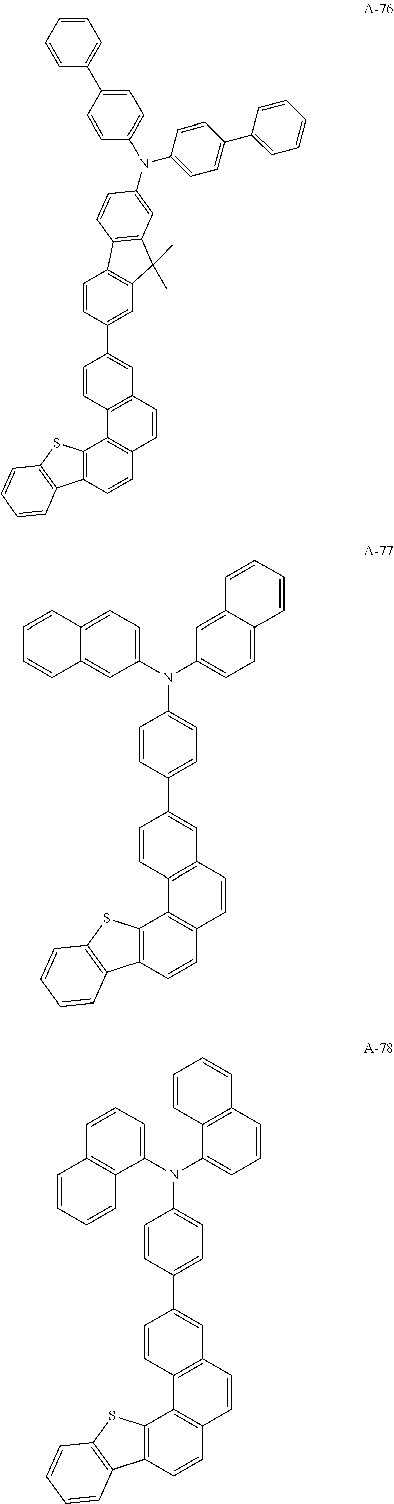


| TABLE 2 | |||||
| Compound | |||||
| used in | Half-life | ||||
| second hole | Driving | life-span | |||
| transport | voltage | Color | Efficiency | (h) @ | |
| Devices | layer (HTL) | (V) | (EL color) | (cd/A) | 1000 cd/m2 |
| Example 1 | A-1 | 6.1 | Blue | 6.5 | 2,030 |
| Example 2 | A-4 | 6.2 | Blue | 6.6 | 2,170 |
| Example 3 | B-2 | 6.1 | Blue | 6.4 | 1,840 |
| Example 4 | A-26 | 6.1 | Blue | 6.6 | 2,260 |
| Example 5 | A-38 | 6.1 | Blue | 6.8 | 1,570 |
| Example 6 | A-111 | 6.0 | Blue | 6.4 | 2,310 |
| Example 7 | A-112 | 6.1 | Blue | 6.5 | 1,790 |
| Compar- | None | 6.4 | Blue | 5.9 | 1,380 |
| ative | |||||
| Example 1 | |||||
| *Current density: 10 mA/cm2 | |||||
-
- 100, 200, 300: organic light emitting diode
- 105: organic layer
- 110: cathode
- 120: anode
- 130: emission layer
- 140: hole transport layer
- 141: first hole transport layer
- 142: second hole transport layer
Claims (12)


Applications Claiming Priority (5)
| Application Number | Priority Date | Filing Date | Title |
|---|---|---|---|
| KR10-2014-0056715 | 2014-05-12 | ||
| KR20140056715 | 2014-05-12 | ||
| KR10-2015-0048885 | 2015-04-07 | ||
| KR1020150048885A KR101904299B1 (en) | 2014-05-12 | 2015-04-07 | Organic compound and organic optoelectric device and display device |
| PCT/KR2015/003528 WO2015174639A1 (en) | 2014-05-12 | 2015-04-08 | Organic compound, organic optoelectric diode, and display device |
Publications (2)
| Publication Number | Publication Date |
|---|---|
| US20160351820A1 US20160351820A1 (en) | 2016-12-01 |
| US10446760B2 true US10446760B2 (en) | 2019-10-15 |
Family
ID=54844255
Family Applications (1)
| Application Number | Title | Priority Date | Filing Date |
|---|---|---|---|
| US15/117,457 Active 2035-05-19 US10446760B2 (en) | 2014-05-12 | 2015-04-08 | Organic compound, organic optoelectric diode, and display device |
Country Status (4)
| Country | Link |
|---|---|
| US (1) | US10446760B2 (en) |
| KR (1) | KR101904299B1 (en) |
| CN (1) | CN106132944B (en) |
| TW (1) | TWI702206B (en) |
Families Citing this family (5)
| Publication number | Priority date | Publication date | Assignee | Title |
|---|---|---|---|---|
| KR101984244B1 (en) * | 2015-09-09 | 2019-05-30 | 삼성에스디아이 주식회사 | Organic compound and organic optoelectric device and display device |
| KR102041588B1 (en) * | 2016-09-29 | 2019-11-06 | 삼성에스디아이 주식회사 | Compound for organic optoelectronic device, composition for organic optoelectronic device and organic optoelectronic device and display device |
| CN108675975A (en) * | 2017-10-17 | 2018-10-19 | 默克专利有限公司 | Material for organic electroluminescence device |
| KR102630640B1 (en) * | 2018-06-08 | 2024-01-30 | 삼성디스플레이 주식회사 | Organic light-emitting device including an amine-based compound and an amine-based compound |
| KR102669040B1 (en) * | 2020-09-22 | 2024-05-27 | 엘티소재주식회사 | Compound and organic light emitting device including the same |
Citations (13)
| Publication number | Priority date | Publication date | Assignee | Title |
|---|---|---|---|---|
| US20110248246A1 (en) | 2010-04-09 | 2011-10-13 | Semiconductor Energy Laboratory Co., Ltd. | Aromatic amine derivative, light-emitting element, light-emitting device, electronic device, and lighting device |
| US20110266526A1 (en) | 2010-04-28 | 2011-11-03 | Universal Display Corporation | Triphenylene-Benzofuran/Benzothiophene/Benzoselenophene Compounds With Substituents Joining To Form Fused Rings |
| KR20120072784A (en) | 2010-12-24 | 2012-07-04 | 에스에프씨 주식회사 | Heterocyclic compounds and organic light-emitting diode including the same |
| KR101165698B1 (en) | 2011-06-14 | 2012-07-18 | 덕산하이메탈(주) | Organic electronic element comprising a new compound, and a new compound and a composition for organic electronic element |
| KR20120116881A (en) | 2011-04-13 | 2012-10-23 | 에스에프씨 주식회사 | Condensed aryl compound and organic light-diode including the same |
| CN102782084A (en) | 2010-03-06 | 2012-11-14 | 默克专利有限公司 | Organic electroluminescent device |
| KR20130007934A (en) | 2011-07-11 | 2013-01-21 | 주식회사 두산 | Organic electroluminescence device using the triphenylene derivative |
| US20130099208A1 (en) * | 2011-10-19 | 2013-04-25 | Samsung Mobile Display Co., Ltd. | Condensed-cyclic compound, method for preparing the condensed-cyclic compound and organic light-emitting device including the condensed-cyclic compound |
| JP2013232520A (en) | 2012-04-27 | 2013-11-14 | Udc Ireland Ltd | Organic electroluminescent element, compound and organic electroluminescent element material usable for the same, and light emitting device, display device and lighting device using said element |
| KR20140019082A (en) | 2012-07-26 | 2014-02-14 | 삼성디스플레이 주식회사 | Novel heterocycle compound and organic light emitting device comprising the same |
| US20140117326A1 (en) | 2012-10-30 | 2014-05-01 | Sun-young Lee | Heterocyclic compound and organic light-emitting device including the same |
| CN103782410A (en) | 2011-09-09 | 2014-05-07 | 株式会社Lg化学 | Material of organic light emitting device and organic light emitting device using same |
| CN104638202A (en) | 2013-11-08 | 2015-05-20 | 北京鼎材科技有限公司 | Organic thin-film transistor and production method thereof |
Family Cites Families (2)
| Publication number | Priority date | Publication date | Assignee | Title |
|---|---|---|---|---|
| CN101165698B (en) * | 2006-10-17 | 2011-07-27 | 华为技术有限公司 | Export permitting method and system |
| KR20130004737A (en) * | 2011-07-04 | 2013-01-14 | 삼성전자주식회사 | Image display method and apparatus |
-
2015
- 2015-04-07 KR KR1020150048885A patent/KR101904299B1/en active Active
- 2015-04-08 US US15/117,457 patent/US10446760B2/en active Active
- 2015-04-08 CN CN201580015585.7A patent/CN106132944B/en active Active
- 2015-05-11 TW TW104114842A patent/TWI702206B/en active
Patent Citations (15)
| Publication number | Priority date | Publication date | Assignee | Title |
|---|---|---|---|---|
| CN102782084A (en) | 2010-03-06 | 2012-11-14 | 默克专利有限公司 | Organic electroluminescent device |
| US20110248246A1 (en) | 2010-04-09 | 2011-10-13 | Semiconductor Energy Laboratory Co., Ltd. | Aromatic amine derivative, light-emitting element, light-emitting device, electronic device, and lighting device |
| US20110266526A1 (en) | 2010-04-28 | 2011-11-03 | Universal Display Corporation | Triphenylene-Benzofuran/Benzothiophene/Benzoselenophene Compounds With Substituents Joining To Form Fused Rings |
| KR20120072784A (en) | 2010-12-24 | 2012-07-04 | 에스에프씨 주식회사 | Heterocyclic compounds and organic light-emitting diode including the same |
| KR20120116881A (en) | 2011-04-13 | 2012-10-23 | 에스에프씨 주식회사 | Condensed aryl compound and organic light-diode including the same |
| KR101165698B1 (en) | 2011-06-14 | 2012-07-18 | 덕산하이메탈(주) | Organic electronic element comprising a new compound, and a new compound and a composition for organic electronic element |
| KR20130007934A (en) | 2011-07-11 | 2013-01-21 | 주식회사 두산 | Organic electroluminescence device using the triphenylene derivative |
| CN103782410A (en) | 2011-09-09 | 2014-05-07 | 株式会社Lg化学 | Material of organic light emitting device and organic light emitting device using same |
| US20130099208A1 (en) * | 2011-10-19 | 2013-04-25 | Samsung Mobile Display Co., Ltd. | Condensed-cyclic compound, method for preparing the condensed-cyclic compound and organic light-emitting device including the condensed-cyclic compound |
| KR20130042901A (en) | 2011-10-19 | 2013-04-29 | 삼성디스플레이 주식회사 | A condensed-cyclic compound and an organic light emitting diode comprising the same |
| JP2013232520A (en) | 2012-04-27 | 2013-11-14 | Udc Ireland Ltd | Organic electroluminescent element, compound and organic electroluminescent element material usable for the same, and light emitting device, display device and lighting device using said element |
| KR20140019082A (en) | 2012-07-26 | 2014-02-14 | 삼성디스플레이 주식회사 | Novel heterocycle compound and organic light emitting device comprising the same |
| US20140117326A1 (en) | 2012-10-30 | 2014-05-01 | Sun-young Lee | Heterocyclic compound and organic light-emitting device including the same |
| CN104638202A (en) | 2013-11-08 | 2015-05-20 | 北京鼎材科技有限公司 | Organic thin-film transistor and production method thereof |
| CN104638202B (en) | 2013-11-08 | 2017-09-29 | 北京鼎材科技有限公司 | A kind of OTFT and preparation method thereof |
Non-Patent Citations (4)
| Title |
|---|
| "Organic nano and molecular devices," May 31, 2010, p. 322 (with English Abstract). |
| "Progress in Hole-Transport Materials for Use in Organic Light-Emitting Diodes," vol. 15 No. 6 Nov. 30, 2003, p. 495-504. |
| Chinese Search Report dated Jul. 14, 2017, of the corresponding Chinese Patent Application No. 291580015585.7. |
| Provisional double patenting rejection over claims of the above-identified appiication; USPTO Office action dated Jun. 27, 2018, in U.S. Appl. No. 15/417,454. |
Also Published As
| Publication number | Publication date |
|---|---|
| TW201602088A (en) | 2016-01-16 |
| CN106132944A (en) | 2016-11-16 |
| US20160351820A1 (en) | 2016-12-01 |
| CN106132944B (en) | 2019-07-16 |
| KR20150129606A (en) | 2015-11-20 |
| TWI702206B (en) | 2020-08-21 |
| KR101904299B1 (en) | 2018-10-04 |
Similar Documents
| Publication | Publication Date | Title |
|---|---|---|
| US9882146B2 (en) | Heterocyclic compound and organic electronic element containing same | |
| US12378207B2 (en) | Heterocyclic compound and organic electroluminescent device comprising same | |
| US10131632B2 (en) | Dopant for organic optoelectronic device, organic optoelectronic device and display device | |
| US11673875B2 (en) | Organic compound, organic optoelectric diode, and display device | |
| US9299935B2 (en) | Nitrogen-containing heterocyclic compounds and organic electronic device comprising the same | |
| US8507904B2 (en) | Compound including indole derivative, organic electronic element using same, and terminal thereof | |
| US20160308142A1 (en) | Condensed cyclic compound and organic light-emitting device including the same | |
| US11723271B2 (en) | Organic compound, and electronic component and electronic device therefor | |
| US20170077416A1 (en) | Compound, organic optoelectronic diode comprising same, and display | |
| US10784447B2 (en) | Organic compound, composition, and organic optoelectronic diode | |
| US10700286B2 (en) | Organic compound and organic optoelectric device and display device | |
| US10446764B2 (en) | Organic compound, composition, organic optoelectric device, and display device | |
| US10991887B2 (en) | Amine compound and organic light-emitting device comprising same | |
| US9290513B2 (en) | Compound containing 5-membered heterocycles, organic electronic device using same, and terminal comprising the latter | |
| US20170250349A1 (en) | Organic compound, organic optoelectric device and display device | |
| US20210130313A1 (en) | Nitrogen-containing compound, electronic component and electronic device | |
| US10446760B2 (en) | Organic compound, organic optoelectric diode, and display device | |
| US12077699B2 (en) | Dopant for organic optoelectronic device, organic optoelectronic device, and display device | |
| US12048240B2 (en) | Organic compound, electronic component and electronic apparatus comprising the same | |
| US10141521B2 (en) | Compound, organic optoelectronic element comprising same, and display device | |
| US12338217B2 (en) | Nitrogen-containing compound, electronic element and electronic device | |
| WO2015174639A1 (en) | Organic compound, organic optoelectric diode, and display device | |
| US9543528B2 (en) | Compound for an organic optoelectric device, organic optoelectric device including the same, and display device including the optoelectric device | |
| US20230180601A1 (en) | Composition for organic optoelectronic element, organic optoelectronic element, and display device |
Legal Events
| Date | Code | Title | Description |
|---|---|---|---|
| AS | Assignment |
Owner name: SAMSUNG SDI CO., LTD., KOREA, REPUBLIC OF Free format text: ASSIGNMENT OF ASSIGNORS INTEREST;ASSIGNORS:SHIN, CHANG-JU;RYU, DONG-WAN;YU, EUN-SUN;AND OTHERS;REEL/FRAME:039376/0668 Effective date: 20160803 |
|
| STPP | Information on status: patent application and granting procedure in general |
Free format text: DOCKETED NEW CASE - READY FOR EXAMINATION |
|
| STPP | Information on status: patent application and granting procedure in general |
Free format text: NOTICE OF ALLOWANCE MAILED -- APPLICATION RECEIVED IN OFFICE OF PUBLICATIONS |
|
| STPP | Information on status: patent application and granting procedure in general |
Free format text: PUBLICATIONS -- ISSUE FEE PAYMENT VERIFIED |
|
| STCF | Information on status: patent grant |
Free format text: PATENTED CASE |
|
| MAFP | Maintenance fee payment |
Free format text: PAYMENT OF MAINTENANCE FEE, 4TH YEAR, LARGE ENTITY (ORIGINAL EVENT CODE: M1551); ENTITY STATUS OF PATENT OWNER: LARGE ENTITY Year of fee payment: 4 |