US10404106B2 - Multi-function frequency conversion charging device - Google Patents
Multi-function frequency conversion charging device Download PDFInfo
- Publication number
- US10404106B2 US10404106B2 US15/853,963 US201715853963A US10404106B2 US 10404106 B2 US10404106 B2 US 10404106B2 US 201715853963 A US201715853963 A US 201715853963A US 10404106 B2 US10404106 B2 US 10404106B2
- Authority
- US
- United States
- Prior art keywords
- frequency
- circuit board
- electronic device
- low
- charging device
- Prior art date
- Legal status (The legal status is an assumption and is not a legal conclusion. Google has not performed a legal analysis and makes no representation as to the accuracy of the status listed.)
- Expired - Fee Related, expires
Links
- 238000006243 chemical reaction Methods 0.000 title claims abstract description 16
- 230000005611 electricity Effects 0.000 claims abstract description 18
- 230000005540 biological transmission Effects 0.000 claims abstract description 14
- 238000001914 filtration Methods 0.000 claims abstract description 4
- 230000000977 initiatory effect Effects 0.000 claims abstract description 4
- 230000009471 action Effects 0.000 claims description 4
- 229910000859 α-Fe Inorganic materials 0.000 claims description 4
- 238000010586 diagram Methods 0.000 description 5
- 230000008878 coupling Effects 0.000 description 3
- 238000010168 coupling process Methods 0.000 description 3
- 238000005859 coupling reaction Methods 0.000 description 3
- 238000005516 engineering process Methods 0.000 description 3
- 230000006698 induction Effects 0.000 description 3
- 230000001939 inductive effect Effects 0.000 description 3
- 230000001131 transforming effect Effects 0.000 description 3
- 230000004907 flux Effects 0.000 description 2
- 230000001413 cellular effect Effects 0.000 description 1
- 230000008859 change Effects 0.000 description 1
- 239000003292 glue Substances 0.000 description 1
- 230000007257 malfunction Effects 0.000 description 1
- 239000002184 metal Substances 0.000 description 1
- 238000000034 method Methods 0.000 description 1
- 230000008520 organization Effects 0.000 description 1
- 230000008569 process Effects 0.000 description 1
- 238000007789 sealing Methods 0.000 description 1
Images


Classifications
-
- H—ELECTRICITY
- H02—GENERATION; CONVERSION OR DISTRIBUTION OF ELECTRIC POWER
- H02J—CIRCUIT ARRANGEMENTS OR SYSTEMS FOR SUPPLYING OR DISTRIBUTING ELECTRIC POWER; SYSTEMS FOR STORING ELECTRIC ENERGY
- H02J50/00—Circuit arrangements or systems for wireless supply or distribution of electric power
- H02J50/40—Circuit arrangements or systems for wireless supply or distribution of electric power using two or more transmitting or receiving devices
-
- H—ELECTRICITY
- H02—GENERATION; CONVERSION OR DISTRIBUTION OF ELECTRIC POWER
- H02J—CIRCUIT ARRANGEMENTS OR SYSTEMS FOR SUPPLYING OR DISTRIBUTING ELECTRIC POWER; SYSTEMS FOR STORING ELECTRIC ENERGY
- H02J50/00—Circuit arrangements or systems for wireless supply or distribution of electric power
- H02J50/10—Circuit arrangements or systems for wireless supply or distribution of electric power using inductive coupling
-
- H—ELECTRICITY
- H02—GENERATION; CONVERSION OR DISTRIBUTION OF ELECTRIC POWER
- H02J—CIRCUIT ARRANGEMENTS OR SYSTEMS FOR SUPPLYING OR DISTRIBUTING ELECTRIC POWER; SYSTEMS FOR STORING ELECTRIC ENERGY
- H02J50/00—Circuit arrangements or systems for wireless supply or distribution of electric power
- H02J50/70—Circuit arrangements or systems for wireless supply or distribution of electric power involving the reduction of electric, magnetic or electromagnetic leakage fields
-
- H02J7/025—
-
- H—ELECTRICITY
- H02—GENERATION; CONVERSION OR DISTRIBUTION OF ELECTRIC POWER
- H02J—CIRCUIT ARRANGEMENTS OR SYSTEMS FOR SUPPLYING OR DISTRIBUTING ELECTRIC POWER; SYSTEMS FOR STORING ELECTRIC ENERGY
- H02J50/00—Circuit arrangements or systems for wireless supply or distribution of electric power
- H02J50/80—Circuit arrangements or systems for wireless supply or distribution of electric power involving the exchange of data, concerning supply or distribution of electric power, between transmitting devices and receiving devices
-
- H—ELECTRICITY
- H02—GENERATION; CONVERSION OR DISTRIBUTION OF ELECTRIC POWER
- H02J—CIRCUIT ARRANGEMENTS OR SYSTEMS FOR SUPPLYING OR DISTRIBUTING ELECTRIC POWER; SYSTEMS FOR STORING ELECTRIC ENERGY
- H02J7/00—Circuit arrangements for charging or depolarising batteries or for supplying loads from batteries
- H02J7/00032—Circuit arrangements for charging or depolarising batteries or for supplying loads from batteries characterised by data exchange
- H02J7/00034—Charger exchanging data with an electronic device, i.e. telephone, whose internal battery is under charge
Definitions
- the present invention provides a multi-function frequency conversion charging device, especially relates to a multi-function frequency conversion charging device which receives the wireless high-frequency charging signal to proceed the charging for an electronic device without wireless charging function or just having the function of low-frequency wireless charging.
- the wireless charging which is called the induction charging or the non-contact inductive charging, is to transmit the power generated by the power supply equipment, the charger, to the electric device by applying a way of the near-field induction, the inductive coupling.
- the power received by the electric device can charge the battery or provide for its own operation.
- the charger needs the electronic circuits to push the coil, and the electric device needs the electronic devices to do the power conversion. Both of them need the coils and the high-frequency filter circuit to satisfy the specification of FCC. Consequently, the cost will be higher than the direct contact one.
- the main objective of the present invention is utilizing a simple structure to provide the high-frequency and low-frequency charging signals which is adapted to various kinds of cellular phones with different charging demands and integrating the technologies of the high-frequency and low-frequency charging to effectively solve the interference problems between them.
- the present invention includes: a first circuit board; a high-frequency receiver module set on the first circuit board to provide for wirelessly connecting with a high-frequency wireless charger to transform and produce electricity; at least one power transmission portion set on the first circuit board and electrically connected with the high-frequency receiver module to electrically connect with an first electronic device having a charging portion selectively for wired charging the first electronic device; a second circuit board set at one side of the first circuit board and electrically connected with the first circuit board; a low-frequency transceiver module set on the second circuit board and electrically connected with the high-frequency receiver module to selectively receive the power initiation of the high-frequency receiver module and wirelessly charge a second electronic device; and at least one magnetic portion set between the first circuit board and the second circuit board to provide for filtering the noise and reducing the interference.
- the high-frequency receiver module can be used to react with the high-frequency wireless charger to produce electricity, and then proceed the wired charging to the first electronic device through the power transmission portion when the user utilizing the present invention to proceed the wireless charging.
- the electricity produced by the high-frequency receiver module will turn to activate the low-frequency transceiver module, and then proceed the wireless charging to the second electronic device through the low-frequency transceiver module if the charging object is the second electronic device which just supports the low-frequency wireless charging.
- the magnetic portion can be utilized to isolate the interference between the high-frequency and low-frequency transceiver module, and so as to exactly achieve the purpose of integrating the high-frequency and low-frequency charging.
- FIG. 1 is a perspective view of the preferred embodiment according to the present invention.
- FIG. 2 is a perspective view of the preferred embodiment by another angle according to the present invention.
- FIG. 3 is a structure block diagram of the preferred embodiment according to the present invention.
- FIG. 4 is a decision block diagram of the preferred embodiment according to the present invention.
- FIG. 5 is an implementation schematic diagram 1 of the preferred embodiment according to the present invention.
- FIG. 6 is a block flow char 1 of the preferred embodiment according to the present invention.
- FIG. 7 is an implementation schematic diagram 2 of the preferred embodiment according to the present invention.
- FIG. 8 is a block flow char 2 of the preferred embodiment according to the present invention.
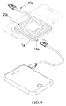
- FIG. 9 is an implementation schematic diagram of another preferred embodiment according to the present invention.
- the present invention includes: a first circuit board 1 ; a high-frequency receiver module 11 set on the first circuit board 1 to provide for wirelessly connecting with a high-frequency wireless charger 7 to transform and produce electricity; at least one power transmission portion 12 set on the first circuit board 1 and electrically connected with the high-frequency receiver module 11 to electrically connect with an first electronic device 5 having a charging portion 51 selectively for wired charging the first electronic device 5 ; wherein the power transmission portion 12 is one of the Mirco USB, Type C USB, and Lightning connector; a second circuit board 2 set at one side of the first circuit board 1 and electrically connected with the first circuit board 1 ; a low-frequency transceiver module 21 set on the second circuit board 2 and electrically connected with the high-frequency receiver module 11 to selectively receive the power initiation of the high-frequency receiver module 11 and wirelessly charge a second electronic device 6 ; wherein the second electronic device 6 has at least one low-frequency charging coil 61 inside to corporately operate with the low-frequency transce
- the present invention has the advantages of small volume and carry convenience.
- the outer-shell body 4 can just be placed at one side of the high-frequency wireless charger 7 to proceed the charging to the first electronic device 5 or the second electronic device 6 through the high-frequency receiver module 11 or the low-frequency transceiver module 21 when using.
- the high-frequency wireless charger 7 of the present invention is majorly for the 6.78 MHz (Mega Hertz) frequency band, therefore it may allow a short distance apart for convenient using when charging because it has an induction range of longer distance than the low-frequency wireless charger.
- the second electronic device 6 of the user adopts the iOS operation system and builds in a low-frequency charging coil 61 in the practical use as shown in FIG. 5 to FIG. 6 , generally the second electronic device 6 cannot use the high-frequency wireless charger 7 to charge because its frequency band is 100 to 300 kHz (kilohertz).
- the present invention can just be placed between the high-frequency wireless charger 7 and the second electronic device 6 to wirelessly connect with the high-frequency wireless charger 7 to receive the high-frequency signals for transforming and producing electricity through using the high-frequency receiver module 11 .
- the user can just place the present invention between the high-frequency wireless charger 7 and the first electronic device 5 to wirelessly connect with the high-frequency wireless charger 7 to receive the high-frequency signals for transforming and producing electricity through using the high-frequency receiver module 11 .
- the user can just place the present invention between the high-frequency wireless charger 7 and the first electronic device 5 to wirelessly connect with the high-frequency wireless charger 7 to receive the high-frequency signals for transforming and producing electricity through using the high-frequency receiver module 11 .
- the difference with the previous embodiment is that the pairing failure of the pairing module 62 will cause malfunction when the high-frequency receiver module 11 transmits the electricity to the low-frequency transceiver module 21 .
- the circuit switching unit 13 on the first circuit board 1 will automatically direct the electricity produced by the high-frequency receiver module 11 to the power transmission portion 12 and let the electricity electrically connect the with the charging portion 51 of the first electronic device 5 through power transmission portion 12 which includes the physical transmission line to make the first electronic device 5 able to receive the signals of the high-frequency wireless charger 7 for achieving the purpose of the indirect wireless charging.
- the magnetic portion 3 is positioned between the first circuit board 1 and the second circuit board 2 according to the present invention, the magnetic portion 3 is a windable the ferrite magnetic film made by sealing the whole ferrite magnetic film with glue in this embodiment. Therefore, it can change the magnetic flux path and reduce the phenomenon of the Eddy current when the magnetic flux closes to the metal.
- this embodiment is almost the same with the previous embodiment.
- the only difference is additionally setting a power receiving portion 14 a on the first circuit board 1 a to provide for receiving the external power supply to replace the electricity produced by the high-frequency receiver module.
Abstract
Description
Claims (10)
Priority Applications (1)
| Application Number | Priority Date | Filing Date | Title |
|---|---|---|---|
| US15/853,963 US10404106B2 (en) | 2017-12-26 | 2017-12-26 | Multi-function frequency conversion charging device |
Applications Claiming Priority (1)
| Application Number | Priority Date | Filing Date | Title |
|---|---|---|---|
| US15/853,963 US10404106B2 (en) | 2017-12-26 | 2017-12-26 | Multi-function frequency conversion charging device |
Publications (2)
| Publication Number | Publication Date |
|---|---|
| US20190199140A1 US20190199140A1 (en) | 2019-06-27 |
| US10404106B2 true US10404106B2 (en) | 2019-09-03 |
Family
ID=66950726
Family Applications (1)
| Application Number | Title | Priority Date | Filing Date |
|---|---|---|---|
| US15/853,963 Expired - Fee Related US10404106B2 (en) | 2017-12-26 | 2017-12-26 | Multi-function frequency conversion charging device |
Country Status (1)
| Country | Link |
|---|---|
| US (1) | US10404106B2 (en) |
Families Citing this family (1)
| Publication number | Priority date | Publication date | Assignee | Title |
|---|---|---|---|---|
| US11183864B2 (en) * | 2018-05-07 | 2021-11-23 | Apple Inc. | Multimode battery charging |
Citations (1)
| Publication number | Priority date | Publication date | Assignee | Title |
|---|---|---|---|---|
| US20180309328A1 (en) * | 2015-12-08 | 2018-10-25 | Maps, Inc. | Wireless power transfer standard selector of power receiving unit and method therefor |
-
2017
- 2017-12-26 US US15/853,963 patent/US10404106B2/en not_active Expired - Fee Related
Patent Citations (1)
| Publication number | Priority date | Publication date | Assignee | Title |
|---|---|---|---|---|
| US20180309328A1 (en) * | 2015-12-08 | 2018-10-25 | Maps, Inc. | Wireless power transfer standard selector of power receiving unit and method therefor |
Also Published As
| Publication number | Publication date |
|---|---|
| US20190199140A1 (en) | 2019-06-27 |
Similar Documents
| Publication | Publication Date | Title |
|---|---|---|
| EP2961034B1 (en) | Coil apparatus of mobile terminal | |
| EP2720383A2 (en) | Wireless power-transmission apparatus and system | |
| JP2013021902A (en) | Non-contact transmission device, and battery unit and battery lid unit having the same | |
| US11296556B2 (en) | Power relay device and system | |
| KR20210129618A (en) | Apparatus for transmitting and receiving wireless power | |
| US10404106B2 (en) | Multi-function frequency conversion charging device | |
| JP2010284066A (en) | Communication device, communication terminal and communication system | |
| JP2018153024A (en) | Transmission apparatus | |
| CN106451805A (en) | Device capable of receiving magnetic induction transmitted by any wireless transmitting terminal | |
| KR20180060578A (en) | Apparatus for receiving wireless power | |
| CN105071024A (en) | Antenna system of mobile terminal | |
| US20200274390A1 (en) | A wireless power transceiver device and an associates method thereof | |
| US10491027B2 (en) | Wireless power transmission | |
| TW202002460A (en) | Micro wave charge management circuit and the method thereof | |
| US20150064970A1 (en) | Systems, apparatus, and methods for an embedded emissions filter circuit in a power cable | |
| US20180269719A1 (en) | Power transmission device | |
| CN205489822U (en) | Novel receiver and transmitter of wireless charger | |
| KR102257626B1 (en) | Hybrid type wireles power receiving device, method of controlling wireless power signal in hybrid type wireles power receiving device, and magnetic resonance type wireless power receiving device related to the same | |
| TWI652875B (en) | Multi-function inverter charging device | |
| JP2018153026A (en) | Transmission apparatus | |
| KR102548981B1 (en) | Apparatus for receiving wireless power | |
| CN109904887A (en) | Multifunctional variable-frequency charging unit | |
| CN111245035A (en) | Device and method capable of realizing remote wireless charging | |
| CN114006480A (en) | Transmitting circuit, receiving circuit, charger and electronic device | |
| KR20180082881A (en) | Coil Of Apparatus For Transmitting And Receiving Wireless Power And Thereof Production Method |
Legal Events
| Date | Code | Title | Description |
|---|---|---|---|
| FEPP | Fee payment procedure |
Free format text: ENTITY STATUS SET TO UNDISCOUNTED (ORIGINAL EVENT CODE: BIG.); ENTITY STATUS OF PATENT OWNER: SMALL ENTITY |
|
| AS | Assignment |
Owner name: KINGDO CLOUD INFORMATION PTE. LTD., SINGAPORE Free format text: ASSIGNMENT OF ASSIGNORS INTEREST;ASSIGNOR:WU, JUAN-HUNG;REEL/FRAME:044494/0489 Effective date: 20171225 |
|
| FEPP | Fee payment procedure |
Free format text: ENTITY STATUS SET TO SMALL (ORIGINAL EVENT CODE: SMAL); ENTITY STATUS OF PATENT OWNER: SMALL ENTITY |
|
| STPP | Information on status: patent application and granting procedure in general |
Free format text: PUBLICATIONS -- ISSUE FEE PAYMENT VERIFIED |
|
| STCF | Information on status: patent grant |
Free format text: PATENTED CASE |
|
| FEPP | Fee payment procedure |
Free format text: MAINTENANCE FEE REMINDER MAILED (ORIGINAL EVENT CODE: REM.); ENTITY STATUS OF PATENT OWNER: SMALL ENTITY |
|
| LAPS | Lapse for failure to pay maintenance fees |
Free format text: PATENT EXPIRED FOR FAILURE TO PAY MAINTENANCE FEES (ORIGINAL EVENT CODE: EXP.); ENTITY STATUS OF PATENT OWNER: SMALL ENTITY |
|
| STCH | Information on status: patent discontinuation |
Free format text: PATENT EXPIRED DUE TO NONPAYMENT OF MAINTENANCE FEES UNDER 37 CFR 1.362 |
|
| FP | Lapsed due to failure to pay maintenance fee |
Effective date: 20230903 |