US10401301B2 - Optical test system and method, and method of manufacturing semiconductor device by using the optical test system and method - Google Patents
Optical test system and method, and method of manufacturing semiconductor device by using the optical test system and method Download PDFInfo
- Publication number
- US10401301B2 US10401301B2 US15/940,011 US201815940011A US10401301B2 US 10401301 B2 US10401301 B2 US 10401301B2 US 201815940011 A US201815940011 A US 201815940011A US 10401301 B2 US10401301 B2 US 10401301B2
- Authority
- US
- United States
- Prior art keywords
- light beam
- polarization state
- reflected light
- reflected
- incident
- Prior art date
- Legal status (The legal status is an assumption and is not a legal conclusion. Google has not performed a legal analysis and makes no representation as to the accuracy of the status listed.)
- Active
Links
Images


Classifications
-
- G—PHYSICS
- G01—MEASURING; TESTING
- G01N—INVESTIGATING OR ANALYSING MATERIALS BY DETERMINING THEIR CHEMICAL OR PHYSICAL PROPERTIES
- G01N21/00—Investigating or analysing materials by the use of optical means, i.e. using sub-millimetre waves, infrared, visible or ultraviolet light
- G01N21/84—Systems specially adapted for particular applications
- G01N21/88—Investigating the presence of flaws or contamination
- G01N21/8806—Specially adapted optical and illumination features
-
- G—PHYSICS
- G01—MEASURING; TESTING
- G01N—INVESTIGATING OR ANALYSING MATERIALS BY DETERMINING THEIR CHEMICAL OR PHYSICAL PROPERTIES
- G01N21/00—Investigating or analysing materials by the use of optical means, i.e. using sub-millimetre waves, infrared, visible or ultraviolet light
- G01N21/17—Systems in which incident light is modified in accordance with the properties of the material investigated
- G01N21/21—Polarisation-affecting properties
-
- G—PHYSICS
- G01—MEASURING; TESTING
- G01N—INVESTIGATING OR ANALYSING MATERIALS BY DETERMINING THEIR CHEMICAL OR PHYSICAL PROPERTIES
- G01N21/00—Investigating or analysing materials by the use of optical means, i.e. using sub-millimetre waves, infrared, visible or ultraviolet light
- G01N21/84—Systems specially adapted for particular applications
- G01N21/88—Investigating the presence of flaws or contamination
- G01N21/95—Investigating the presence of flaws or contamination characterised by the material or shape of the object to be examined
- G01N21/9501—Semiconductor wafers
-
- G—PHYSICS
- G01—MEASURING; TESTING
- G01N—INVESTIGATING OR ANALYSING MATERIALS BY DETERMINING THEIR CHEMICAL OR PHYSICAL PROPERTIES
- G01N21/00—Investigating or analysing materials by the use of optical means, i.e. using sub-millimetre waves, infrared, visible or ultraviolet light
- G01N21/84—Systems specially adapted for particular applications
- G01N21/88—Investigating the presence of flaws or contamination
- G01N21/95—Investigating the presence of flaws or contamination characterised by the material or shape of the object to be examined
- G01N21/956—Inspecting patterns on the surface of objects
-
- H—ELECTRICITY
- H01—ELECTRIC ELEMENTS
- H01L—SEMICONDUCTOR DEVICES NOT COVERED BY CLASS H10
- H01L21/00—Processes or apparatus adapted for the manufacture or treatment of semiconductor or solid state devices or of parts thereof
- H01L21/67—Apparatus specially adapted for handling semiconductor or electric solid state devices during manufacture or treatment thereof; Apparatus specially adapted for handling wafers during manufacture or treatment of semiconductor or electric solid state devices or components ; Apparatus not specifically provided for elsewhere
- H01L21/67005—Apparatus not specifically provided for elsewhere
- H01L21/67242—Apparatus for monitoring, sorting or marking
- H01L21/67288—Monitoring of warpage, curvature, damage, defects or the like
-
- H—ELECTRICITY
- H01—ELECTRIC ELEMENTS
- H01L—SEMICONDUCTOR DEVICES NOT COVERED BY CLASS H10
- H01L22/00—Testing or measuring during manufacture or treatment; Reliability measurements, i.e. testing of parts without further processing to modify the parts as such; Structural arrangements therefor
- H01L22/10—Measuring as part of the manufacturing process
- H01L22/12—Measuring as part of the manufacturing process for structural parameters, e.g. thickness, line width, refractive index, temperature, warp, bond strength, defects, optical inspection, electrical measurement of structural dimensions, metallurgic measurement of diffusions
-
- H—ELECTRICITY
- H01—ELECTRIC ELEMENTS
- H01L—SEMICONDUCTOR DEVICES NOT COVERED BY CLASS H10
- H01L22/00—Testing or measuring during manufacture or treatment; Reliability measurements, i.e. testing of parts without further processing to modify the parts as such; Structural arrangements therefor
- H01L22/20—Sequence of activities consisting of a plurality of measurements, corrections, marking or sorting steps
- H01L22/24—Optical enhancement of defects or not directly visible states, e.g. selective electrolytic deposition, bubbles in liquids, light emission, colour change
-
- H—ELECTRICITY
- H01—ELECTRIC ELEMENTS
- H01L—SEMICONDUCTOR DEVICES NOT COVERED BY CLASS H10
- H01L22/00—Testing or measuring during manufacture or treatment; Reliability measurements, i.e. testing of parts without further processing to modify the parts as such; Structural arrangements therefor
- H01L22/30—Structural arrangements specially adapted for testing or measuring during manufacture or treatment, or specially adapted for reliability measurements
-
- G—PHYSICS
- G01—MEASURING; TESTING
- G01N—INVESTIGATING OR ANALYSING MATERIALS BY DETERMINING THEIR CHEMICAL OR PHYSICAL PROPERTIES
- G01N21/00—Investigating or analysing materials by the use of optical means, i.e. using sub-millimetre waves, infrared, visible or ultraviolet light
- G01N21/84—Systems specially adapted for particular applications
- G01N21/88—Investigating the presence of flaws or contamination
- G01N21/8806—Specially adapted optical and illumination features
- G01N2021/8848—Polarisation of light
-
- G—PHYSICS
- G01—MEASURING; TESTING
- G01N—INVESTIGATING OR ANALYSING MATERIALS BY DETERMINING THEIR CHEMICAL OR PHYSICAL PROPERTIES
- G01N2201/00—Features of devices classified in G01N21/00
- G01N2201/06—Illumination; Optics
- G01N2201/068—Optics, miscellaneous
- G01N2201/0683—Brewster plate; polarisation controlling elements
Definitions
- Embodiments relate to an optical test system and method, and a method of manufacturing a semiconductor device by using the optical test system and method.
- Defects existing in the surface of a semiconductor wafer or a semiconductor device can affect the reliability and yield of the semiconductor wafer or the semiconductor device.
- various methods using light can be utilized.
- a defect of a certain size or less may be difficult to distinguish from noise due to the roughness of the surface of the semiconductor wafer or the semiconductor device.
- an optical test system including a stage region to accommodate an object to be tested, a first incident optical system to change a first polarization state of a first light beam to a second polarization state and to provide the first light beam in the second polarization state to the stage region in a first direction at a first incident angle which is not a right angle, a second incident optical system to change a third polarization state of a second light beam to a fourth polarization state and to provide the second light beam in the fourth polarization state to the stage region in a second direction, which is different from the first direction by a first angle, at a second incident angle which is not a right angle, and a main optical system to detect a first reflected light beam reflected at a first reflection angle different from the first and second incident angles among a plurality of reflected light beams obtained after the first light beam in the second polarization state is reflected from the stage region.
- a method of manufacturing a semiconductor device including providing an object to be tested and performing an optical test on the object to be tested.
- Performing the optical test on the object to be tested includes changing a first polarization state of a first light beam to a second polarization state, providing the first light beam in the second polarization state to a test region of the object to be tested in a first direction at a first incident angle which is not a right angle, detecting a first reflected light beam reflected at a first reflection angle different from the first incident angle among a plurality of reflected light beams obtained after the first light beam in the second polarization state is incident on the test region and then reflected from the test region, obtaining first image data by using the first reflected light beam, changing a third polarization state of a second light beam to a fourth polarization state, providing the second light beam in the fourth polarization state to the test region in a second direction, which is different from the first direction by a first angle, at a second
- an optical test method comprising, changing a first polarization state of a first light beam to a second polarization state, providing the first light beam in the second polarization state to a stage region in a first direction at a first incident angle which is not a right angle, detecting a first reflected light beam reflected at a first reflection angle different from the first incident angle among a plurality of reflected light beams obtained after the first light beam in the second polarization state is reflected from the stage region, changing a third polarization state of a second light beam to a fourth polarization state, providing the second light beam in the fourth polarization state to the stage region in a second direction, which is different from the first direction by a first angle, at a second incident angle which is not a right angle, and detecting a second reflected light beam reflected at a second reflection angle different from the second incident angle among the reflected light beams obtained after the second light beam in the fourth polarization state is incident on the stage region and then
- FIG. 1 illustrates a conceptual plan view of an optical test system according to embodiments
- FIG. 2 illustrates an object to be tested and a test region of FIG. 1 ;
- FIG. 3 illustrates a side view of the optical test system of FIG. 1 to describe the optical test system according to the embodiments;
- FIG. 4 illustrates a first polarized light generator of FIG. 3 ;
- FIG. 5 illustrates a diagram for explaining a first change condition and a first blocking condition of the optical test system of FIG. 1 ;
- FIG. 6 illustrates a main optical system and an image processor included in the optical test system of FIG. 1 ;
- FIG. 7 illustrates the main optical system of FIG. 6 ;
- FIG. 8 illustrates the image processor of FIG. 6 ;
- FIG. 9 illustrates a conceptual plan view of an optical test system according to embodiments.
- FIG. 10 illustrates a side view of the optical test system of FIG. 9 to describe the optical test system according to the embodiments
- FIG. 11 illustrates a main optical system of FIG. 10 ;
- FIG. 12 illustrates a conceptual plan view of an optical test system according to embodiments.
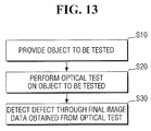
- FIGS. 13 and 14 respectively illustrate flowcharts of an optical test method and a method of manufacturing a semiconductor device by using the optical test method according to embodiments.
- FIGS. 1 through 8 An optical test system according to embodiments will now be described with reference to FIGS. 1 through 8 .
- FIG. 1 is a conceptual plan view of an optical test system according to embodiments.
- FIG. 2 illustrates an object 103 to be tested and a test region TR 1 of FIG. 1 .
- FIG. 3 shows a side view of the optical test system of FIG. 1 to describe the optical test system according to the embodiments.
- a third incident optical system 203 a fourth incident optical system 204 , a third sub-optical system 303 and a fourth sub-optical system 304 of FIG. 1 are omitted for clarity of illustration.
- FIG. 4 illustrates a first polarized light generator 221 of FIG. 3 .
- the optical test system may include first through fourth incident optical systems 201 through 204 , first through fourth sub-optical systems 301 through 304 , and a stage 101 for receiving the object 103 to be tested.
- a stage region SR may include the stage 101 for receiving the object 103 to be tested.
- the object 103 to be tested may be, for example, a semiconductor wafer or a patterned semiconductor device.
- a plurality of regions of the object 103 to be tested may include the test region TR 1 which is a region to be tested by the optical test system.
- the first through fourth incident optical systems 201 , 202 , 203 , and 204 may be disposed in different directions from the stage region SR (specifically, the test region TR 1 ).
- the first incident optical system 201 may be disposed in a first direction D 1 from the test region TR 1 .
- the second incident optical system 202 may be disposed in a second direction D 2 which is different from the first direction D 1 by a first angle ⁇ 1 . That is, the second incident optical system 202 may be separated from the first incident optical system 201 by the first angle ⁇ 1 .
- the third incident optical system 203 may be disposed in a third direction D 3 which is different from the first direction D 1 by the sum of the first angle ⁇ 1 and a second angle ⁇ 2 . That is, the third incident optical system 203 may be separated from the second incident optical system 202 by the second angle ⁇ 2 .
- the fourth incident optical system 204 may be disposed in a fourth direction D 4 which is different from the first direction D 1 by the sum of the first angle ⁇ 1 , the second angle ⁇ 2 and a third angle ⁇ 3 . That is, the fourth incident optical system 204 may be separated from the third incident optical system 203 by the third angle ⁇ 3 .
- the first through fourth sub-optical systems 301 , 302 , 303 . and 304 may be placed to correspond to the first through fourth incident optical systems 201 through 204 , respectively.
- the first sub-optical system 301 may be placed to face the first incident optical system 201 in the first direction D 1 .
- the first sub-optical system 301 may be separated from the fourth incident optical system 204 by a fourth angle ⁇ 4 .
- the second sub-optical system 302 may be placed to face the second incident optical system 202 in the second direction D 2 .
- the second sub-optical system 302 may be separated from the first sub-optical system 301 by the first angle ⁇ 1 .
- the third sub-optical system 303 may be placed to face the third incident optical system 203 in the third direction D 3 .
- the third sub-optical system 303 may be separated from the second sub-optical system 302 by the second angle ⁇ 2 .
- the fourth sub-optical system 304 may be placed to face the fourth incident optical system 204 in the fourth direction D 4 .
- the fourth sub-optical system 304 may be separated from the third sub-optical system 303 by the third angle ⁇ 3 .
- the fourth sub-optical system 304 may be separated from the first incident optical system 201 by the fourth angle ⁇ 4 .
- the first through fourth incident optical systems 201 , 202 , 203 , and 204 may be paired with the first through fourth sub-optical systems 301 through 304 , respectively.
- the first incident optical system 201 may be paired with the first sub-optical system 301 .
- the first incident optical system 201 and the first sub-optical system 301 are paired with each other, they may face each other in the same plane.
- the sum of the first through fourth angles ⁇ 1 through ⁇ 4 may be 180 degrees.
- n (n is a natural number) incident optical systems are arranged between the first incident optical system 201 and the first sub-optical system 301 , the sum of an angle from the direction in which the first incident optical system 201 is disposed to a direction in which an n th incident optical system is disposed and an angle from the direction in which the n th incident optical system is disposed to the direction in which the first sub-optical system 301 is disposed may be 180 degrees.
- the first through fourth incident optical systems 201 , 202 , 203 , and 204 , and the first through fourth sub-optical systems 301 , 302 , 303 , and 304 may simultaneously perform an optical test on the test region TR 1 .
- the first through fourth incident optical systems 201 , 202 , 203 and 204 , and the first through fourth sub-optical systems 301 , 302 , 303 , and 304 may sequentially perform an optical test on the test region TRI.
- the first incident optical system 201 and the first sub-optical system 301 may test the test area TR 1 at a position in the first direction D 1 . Then, the first incident optical system 201 and the first sub-optical system 301 may move to a position where the second incident optical system 202 and the second sub-optical system 302 illustrated in FIG. 1 are disposed and test the test region TR 1 at the position in the second direction D 2 .
- the second through fourth incident optical systems 202 through 204 and the second through fourth sub-optical systems 302 through 304 illustrated in FIG. 1 indicate a trajectory along which the first incident optical system 201 and the first sub-optical system 301 move to perform an optical test.
- the first incident optical system 201 may include a first light source 211 and a first polarized light generator 221 .
- the first light source 211 may provide a first light beam IL 11 in a first polarization state to the first polarized light generator 221 .
- the first polarized light generator 221 may change the first polarization state of the first light beam IL 11 to a second polarization state.
- a first light beam IL 12 in the second polarization state may be incident on the stage region SR at a first incident angle a 11 .
- the second polarization state may be, e.g., an elliptical polarization state. That is, the first polarized light generator 221 may change the polarization state of incident light to, e.g., the elliptical polarization state.
- the first polarized light generator 221 may include, e.g., a first polarizer 221 _ 1 and a compensator 221 _ 2 .
- the first polarizer 221 _ 1 and the compensator 221 _ 2 may change the first light beam IL 11 in the first polarization state to the first light beam IL 12 in the second polarization state.
- each of the first polarizer 221 _ 1 and the compensator 221 _ 2 may be rotated according to a first change condition in order to change the first light beam IL 11 in the first polarization state to the first light beam IL 12 in the second polarization state.
- the first change condition and the rotation of each of the first polarizer 221 _ 1 and the compensator 221 _ 2 will be described in detail later.
- the first light source 211 and the first polarized light generator 221 may provide the first light beam IL 12 in the second polarization state to the test region TR 1 at the first incident angle a 11 .
- the first incident angle a 11 may be a value measured based on a virtual line L 0 perpendicular to an upper surface of the stage 101 .
- the first incident optical system 201 may provide the first light beam IL 12 in the second polarization state to the stage region SR in the first direction D 1 at the first incident angle a 11 .
- the second incident optical system 202 may include a second light source 212 and a second polarized light generator 222 .
- the second light source 212 may provide a second light beam IL 21 in a third polarization state to the second polarized light generator 222 .
- the second polarized light generator 222 may change the third polarization state to a fourth polarization state.
- a second light beam IL 22 in the fourth polarization state may be incident on the stage region SR at a second incident angle a 21 .
- the fourth polarization state may be, e.g., an elliptical polarization state. That is, the second polarized light generator 222 may change the polarization state of incident light to, e.g., the elliptical polarization state.
- the second polarized light generator 222 may include, e.g., a second polarizer and a compensator.
- the second polarizer and the compensator may change the second light beam IL 21 in the third polarization state to the second light beam IL 22 in the fourth polarization state.
- each of the second polarizer and the compensator may be rotated according to a second change condition in order to change the second light beam IL 21 in the third polarization state to the second light beam IL 22 in the fourth polarization state.
- the second change condition and the rotation of each of the second polarizer and the compensator will be described in detail later.
- the second light source 212 and the second polarized light generator 222 may provide the second light beam IL 22 in the fourth polarization state to the test region TR 1 at the second incident angle a 21 .
- the second incident angle a 21 may be a value measured based on the virtual line L 0 perpendicular to the upper surface of the stage 101 .
- the second incident optical system 202 may provide the second light beam IL 22 in the fourth polarization state to the stage region SR in the second direction D 2 at the second incident angle a 21 .
- each of the third incident optical system 203 and the fourth incident optical system 204 may include a light source and a polarized light generator for changing the polarization state of light generated from the light source.
- Light beams that pass through the polarized light generators may be incident on the stage region SR at third and fourth incident angles which are not right angles.
- the polarized light generator of each of the third incident optical system 203 and the fourth incident optical system 204 may also include a polarizer and a compensator.
- the polarizer and the compensator included in the polarized light generator of each of the third incident optical system 203 and the fourth incident optical system 204 may be rotated at a certain angle to change the polarization state.
- the first incident angle a 11 , the second incident angle a 21 , the third incident angle, and the fourth incident angle may be the same.
- the first incident angle a 11 and the second incident angle a 21 may not be right angles. Further, the incident angle of a light beam provided to the stage region SR by each of the third incident optical system 203 and the fourth incident optical system 204 may not be right angles. In other words, light beams provided to the stage region SR by the first through fourth incident optical systems 201 , 202 , 203 , and 204 may not be perpendicular to the upper surface of the stage 101 , e.g., at an angle relative to the virtual line L 0 .
- each of the first through fourth incident optical systems 201 , 202 , 203 , and 204 includes a light source and a polarized light generator
- the technical idea of embodiments is not limited to this case.
- each of the first through fourth incident optical systems 201 , 202 , 203 , and 204 may include various elements for elliptically polarizing light to be incident on the stage region SR, such as a monochromator or a collimator.
- a plurality of reflected light beams may include light beams reflected from the stage region SR after being incident on the stage region SR by the first through fourth incident optical systems 201 through 204 .
- the first through fourth sub-optical systems 301 , 302 , 303 , and 304 may receive specularly reflected light beams among the reflected light beams (e.g., DL 11 , DL 12 , RL 1 , RL 2 , and N 1 ) obtained after the light beams incident on the stage region SR by the first through fourth incident optical systems 201 , 202 , 203 and 204 are reflected from the stage region SR.
- the specularly reflected light beams are RL 1 and RL 2 .
- Reflected light beams (e.g., DL 11 , DL 12 , and N 1 ) other than the specularly reflected light beams from the reflected light beams (e.g., DL 11 , DL 12 , RL 1 , RL 2 , and N 1 ), e.g., noise and diffusely reflected light beams, may be received by a main optical system 400 , described in detail later.
- Each of the reflected light beams (e.g., DL 11 , DL 12 , and N 1 ) other than the specularly reflected light beams (e.g., RL 1 and RL 2 ) may be a light beam reflected from the stage region SR at a reflection angle (e.g., a third reflection angle b 1 or a fourth reflection angle b 2 ) different in size from each of the first incident angle a 11 and the second incident angle a 21 .
- each of the third reflection angle b 1 and the fourth reflection angle b 2 may not be the same as, e.g., may be different from, any of the first incident angle a 11 and the second incident angle a 21 .
- different means having a different absolute value relative to the virtual line L 0 .
- each of the third reflection angle b 1 and the fourth reflection angle b 2 may not be the same as, e.g., may be different from, the incident angles of light beams incident on the stage region SR by the third and fourth incident optical systems 203 and 204 .
- the main optical system 400 will be described in detail later.
- the first sub-optical system 301 may receive a first reflected light beam RL 1 obtained after the first light beam IL 12 in the second polarized state incident on the stage region SR is specularly reflected.
- the first reflected light beam RL 1 may be a light beam reflected from the stage region SR at a first reflection angle a 12 .
- the first reflection angle a 12 may be the same as the first incident angle a 11 .
- the same is to mean having a same absolute value relative to the virtual line L 0 .
- the first reflected light beam RL 1 may be, for example, a linearly polarized light beam.
- the first sub-optical system 301 may include a first sub-polarizer 311 .
- the first sub-polarizer 311 may receive the first reflected light beam RL 1 and transmit a portion of the amount of the first reflected light beam RL 1 .
- the first sub-polarizer 311 may pass about 1/200,000 th or less of the amount of the first reflected light RL 1 .
- the first sub-polarizer 311 may block, e.g., completely block, the received first reflected light beam RL 1 .
- the first sub-polarizer 311 may be rotated according to a first blocking condition in order to transmit a portion of the amount of the first reflected light beam RL 1 or block the first reflected light beam RL 1 .
- the first sub-optical system 301 may further include, for example, a detector.
- the detector may detect light tranmitted from the first sub-polarizer 311 and generate an image of the detected light.
- the detector may be a charge coupled device (CCD).
- the first reflected light beam RL 1 may be blocked, e.g., completely blocked, by the first sub-polarizer 311 under the first blocking condition.
- the first reflected light beam RL 1 may include a light component blocked by the first sub-polarizer 311 and a light component DL 0 not blocked, e.g., transmitted, by the first sub-polarizer 311 under the first blocking condition.
- the detector of the first sub-optical system 301 may detect the light component DL 0 not blocked by the first sub-polarizer 311 .
- the light component DL 0 not blocked by the first sub-polarizer 311 under the first blocking condition may indicate that a defect exists in the test region TR 1 .
- the test region TRI when the test region TRI is not defective, only a portion of the amount of the first reflected light beam RL 1 may pass through the first sub-polarizer 311 under the first blocking condition.
- the light component DL 0 passing through the first sub-polarizer 311 may include the portion of the amount of the first reflected light beam RL 1 and another portion of the amount of the first reflected light beam RL 1 under the first blocking condition.
- the another portion of the amount of the first reflected light beam RL 1 from the light component DL 0 may indicate that a defect exists in the test region TR 1 .
- the first blocking condition and the rotation of the first sub-polarizer 311 will be described in more detail later.
- the second sub-optical system 302 may receive a second reflected light beam RL 2 obtained after the second light beam IL 22 in the fourth polarization state incident on the stage region SR is specularly reflected.
- the second reflected light beam RL 2 may be a light beam reflected from the stage region SR at a second reflection angle a 22 .
- the second reflection angle a 22 may be the same as the second incident angle a 21 .
- the second reflected light beam RL 2 may be, e.g., a linearly polarized light beam.
- the second sub-optical system 302 may include a second sub-polarizer 312 .
- the second through fourth sub-optical systems 302 through 304 may perform substantially similar functions to the first sub-optical system 301 .
- FIG. 5 is a diagram for explaining the first change condition and the first blocking condition of the optical test system of FIG. 1 . For clarity, any redundant description will be omitted.
- the first light beam IL 11 in the first polarization state may pass through the first polarizer 221 _ 1 to be incident on the compensator 221 _ 2 .
- the first light beam IL 11 passing through the compensator 221 _ 2 may be the first light beam IL 12 in the second polarization state.
- the first polarizer 221 _ 1 and the compensator 221 _ 2 may be rotated at a certain angle according to the first change condition in order to change the first light beam IL 11 in the first polarization state to the first light beam IL 12 in the second polarization state.
- first and second x-axis directions X 1 and X 2 may be perpendicular to the traveling direction of the first light beam IL 11 in the first polarization state.
- the first and second x-axis directions X 1 and X 2 may be, e.g., p-polarization directions.
- First and second y-axis directions Y 1 and Y 2 may intersect the first and second x-axis directions X 1 and X 2 and the travelling direction of the first light beam IL 11 in the first polarization state and may be perpendicular to the first and second x-axis directions X 1 and X 2 and the traveling direction of the first light beam IL 11 in the first polarization state, respectively.
- the first and second y-axis directions Y 1 and Y 2 may be, e.g., s-polarization directions.
- a polarization direction 221 _ 1 P of the first polarizer 221 _ 1 may be rotated by a first rotation angle C 1 with respect to the first x-axis direction X 1 .
- a polarization direction 221 _ 2 P of the compensator 221 _ 2 may be rotated by a second rotation angle C 2 with respect to the second x-axis direction X 2 .
- the first rotation angle C 1 and the second rotation angle C 2 may be included in the first change condition.
- the first light beam IL 11 in the first polarization state may be changed into the first light beam IL 12 in the second polarization state.
- the first sub-polarizer 311 may be rotated at a certain angle according to the first blocking condition in order to block the first reflected light beam RL 1 in the linear polarization state or to pass only a portion of the amount of the first reflected light beam RL 1 .
- a third x-axis direction X 3 may be perpendicular to the traveling direction of the first reflected light RL 1 .
- the third x-axis direction X 3 may be, e.g., a p-polarization direction.
- a third y-axis direction Y 3 may intersect the third x-axis direction X 3 and the traveling direction of the first reflected light beam RL 1 and may be perpendicular to the third x-axis direction X 3 and the travelling direction of the first reflected light beam RL 1 .
- the third y-axis direction Y 3 may be, for example, an s-polarization direction.
- a polarization direction 311 P of the first sub-polarizer 311 may be rotated by a third rotation angle C 3 with respect to the third x-axis direction X 3 .
- the third rotation angle C 3 may be included in the first blocking condition.
- the first reflected light beam RL 1 may be blocked by the first sub-polarizer 311 or a portion of the amount of the first reflected light beam RL 1 may be passed.
- the first polarizer 221 _ 1 , the compensator 221 _ 2 , and the first sub-polarizer 311 are rotated in a clockwise direction with respect to the traveling direction of the first light beam IL 11 and IL 12 and the first reflected light beam RL 1 .
- the technical idea of embodiments is not limited to this case.
- each of the first polarizer 221 _ 1 , the compensator 221 _ 2 , and the first sub-polarizer 311 may also be rotated in a counterclockwise direction.
- the first change condition (the first and second rotation angles C 1 and C 2 ) and the first blocking condition (the third rotation angle C 3 ) may be obtained using equations (Equations 1 and 2) for a complex amplitude (E (C 1 , C 2 , C 3 )) and an elliptical polarization coefficient ( ⁇ , ⁇ ) of the first reflected light beam RL 1 and an equation (Equation 3) for the intensity of light.
- Equation 1 Equations 1 and 2 for a complex amplitude (E (C 1 , C 2 , C 3 )) and an elliptical polarization coefficient ( ⁇ , ⁇ ) of the first reflected light beam RL 1 and an equation (Equation 3) for the intensity of light.
- Equation 3 Equation 3
- r p is a reflection coefficient of the test region TR 1 for p-polarized light
- r s is a reflection coefficient of the test region TR 1 for s-polarized light.
- the elliptical polarization coefficient ( ⁇ , ⁇ ) can be obtained as in Equations 5 and 6 by using I(0, ⁇ /4, 0), I(0, ⁇ /4, ⁇ /4), and I( ⁇ /4, ⁇ /4, ⁇ /2).
- Equation 1 can be rearranged into Equation 7.
- Equations 1 through 6 are used to obtain the elliptical polarization coefficient ( ⁇ , ⁇ )
- the technical idea of embodiments is not limited to this case.
- the elliptical polarization coefficient ( ⁇ , ⁇ ) can be obtained using other equations.
- the technical idea of embodiments is not limited to this case.
- the first blocking condition and the first change condition can be obtained using equations different from Equations 1 through 9.
- the first blocking condition and the first change condition can be obtained experimentally.
- the first through fourth change conditions of the first through fourth incident optical systems 201 , 202 , 203 , and 204 may be different from each other.
- the first through fourth blocking conditions of the first through fourth sub-optical systems 301 , 302 , 303 , and 304 may be different from each other.
- FIG. 6 illustrates the main optical system 400 and an image processor 450 included in the optical test system of FIG. 1 .
- FIG. 7 illustrates the main optical system 400 of FIG. 6 .
- FIG. 8 illustrates the image processor 450 of FIG. 6 .
- any redundant description will be omitted.
- the main optical system 400 may receive reflected light beams DL 1 reflected at reflection angles different from the first incident angle a 11 among a plurality of reflected light beams (e.g., DL 11 , DL 12 , RL 1 , and N 1 ) obtained after the first light beam IL 12 in the second polarization state is reflected from the stage region SR.
- the reflected light beams DL 1 reflected at the reflection angles different from the first incident angle a 11 may include, e.g., a first noise N 1 , a third reflected light beam DL 11 , and a fourth reflected light beam DL 12 .
- the third reflected light beam DL 11 may be a light beam reflected at the third reflection angle b 1 and the fourth reflected light beam DL 12 may be a light beam reflected at the fourth reflection angle b 2 .
- the third reflection angle b 1 and the fourth reflection angle b 2 may be closer to the virtual line L 0 than any of the incident angles.
- the first reflected light beam RL 1 reflected at the first reflection angle a 12 which is the same as the first incident angle a 11 , may not be incident on the main optical system 400 .
- the main optical system 400 may be positioned perpendicular to the stage region SR.
- the first noise N 1 , the third reflected light beam DL 11 , and the fourth reflected light beam DL 12 may be incident on an analyzer 403 through a lens 401 .
- the analyzer 403 may be rotated at a certain angle to remove noise from incident light. For example, the analyzer 403 may pass the third reflected light beam DL 11 and the fourth reflected light beam DL 12 among the first noise N 1 , the third reflected light beam DL 11 , and the fourth reflected light beam DL 12 . The third reflected light beam DL 11 and the fourth reflected light beam DL 12 that pass through the analyzer 403 may be incident on a light detector 404 .
- the rotation angle of the analyzer 403 may be calculated using the third rotation angle C 3 , but the technical idea of embodiments is not limited to this case. For example, the rotation angle of the analyzer 403 may be experimentally determined to remove noise.
- the light detector 404 may generate first image data S 1 and second image data S 2 for the third reflected light beam DL 11 and the fourth reflected light beam DL 12 using the third reflected light beam DL 11 and the fourth reflected light beam DL 12 , respectively.
- the main optical system 400 may provide generated image data S to the image processor 450 .
- the image data S may include the first image data S 1 and the second image data S 2 .
- the image processor 450 may process the image data S to generate final image data SF.
- the final image data SF may include information about a defect existing in the object 103 .
- the image processor 450 is disposed separately from the main optical system 400 .
- embodiments are not limited to this case.
- the image processor 450 may be included in the main optical system 400 .
- FIG. 9 is a conceptual plan view of an optical test system according to embodiments.
- a main optical system 400 and an image processor 450 are omitted for clarity.
- FIG. 10 shows a side view of the optical test system of FIG. 9 to describe the optical test system according to the embodiments.
- FIG. 11 illustrates the main optical system 400 of FIG. 10 .
- a fifth incident optical system 205 and a fifth sub-optical system 305 corresponding to the fifth incident optical system 205 may be separated from a first incident optical system 201 and a first sub-optical system 301 in a first direction D 1 .
- the fifth incident optical system 205 and the fifth sub-optical system 305 corresponding to the fifth incident optical system 205 may be paired with each other.
- the fifth incident optical system 205 may include a fifth light source 215 and a fifth polarized light generator 225 .
- the fifth light source 215 may provide a fifth light beam IL 51 in a fifth polarization state to the fifth polarized light generator 225 .
- the fifth polarized light generator 225 may change the fifth polarization state of the fifth light beam IL 51 to a sixth polarization state.
- a fifth light beam IL 52 in the sixth polarization state may be incident on a stage region SR at a fifth incident angle a 51 .
- the sixth polarization state may be, e.g., an elliptical polarization state. That is, the fifth polarized light generator 225 may change the polarization state of incident light to, e.g., the elliptical polarization state.
- the fifth light source 215 and the fifth polarized light generator 225 may provide the fifth light beam IL 52 in the sixth polarization state to a test region TR 1 at the fifth incident angle a 51 .
- the fifth incident angle a 51 may be a value relative to the virtual line L 0 perpendicular to the upper surface of the stage 101 .
- the fifth incident optical system 205 may provide the fifth light beam IL 52 in the sixth polarization state to the stage region SR in the first direction D 1 at the fifth incident angle a 51 .
- the fifth incident angle a 51 may not be a right angle. In other words, light beams incident on the stage region SR by the fifth incident optical system 205 may not be perpendicular to the upper surface of the stage 101 . In some embodiments, the fifth incident angle a 51 may have a different value from a first incident angle a 11 .
- a plurality of reflected light beams may include reflected light beams DL 51 and N 2 obtained after the fifth light beam IL 52 in the sixth polarization state is reflected from the stage region SR.
- the fifth sub-optical system 305 may receive a fifth reflected light beam RL 5 obtained after the fifth light beam IL 52 in the sixth polarization state is specularly reflected from the stage region SR, among the reflected light beams (e.g., DL 11 , DL 51 , DL 12 , RL 1 , RL 5 , N 1 , and N 2 ).
- the fifth reflected light beam RL 5 may be a light beam reflected from the stage region SR at a fifth reflection angle a 52 .
- the fifth reflection angle a 52 may be the same as the fifth incident angle a 51 .
- the fifth reflected light beam RL 5 may be, for example, a linearly polarized light beam.
- Light beams (e.g., DL 11 , DL 51 , DL 12 , N 1 , and N 2 ) other than the fifth specularly reflected light beam RL 5 from the reflected light beams (e.g., DL 11 , DL 51 , DL 12 , RL 1 , RL 5 , N 1 and N 2 ) may be received by the main optical system 400 .
- Each of the reflected light beams (e.g., DL 11 , DL 51 , DL 12 , N 1 , and N 2 ) other than the fifth specularly reflected light beam RL 5 from the reflected light beams (e.g., DL 11 , DL 51 , DL 12 , RL 1 , RL 5 , N 1 , and N 2 ) may be a light beam reflected from the stage region SR at a reflection angle different from the fifth incident angle a 51 .
- a sixth reflection angle b 3 may not be the same as any of the first incident angle a 11 and the fifth incident angle a 51 .
- the fifth sub-optical system 305 may include a fifth sub-polarizer 315 .
- the fifth sub-polarizer 315 may be substantially similar to a first sub-polarizer 311 .
- a fifth blocking condition may be different from the first blocking condition.
- the function of the fifth sub-polarizer 315 may be substantially the same as that of the first sub-polarizer 311 .
- the main optical system 400 may receive reflected light beams DL 2 reflected at reflection angles different from the first and second incident angles a 11 and a 51 among a plurality of reflected light beams (e.g., DL 11 , DL 51 , DL 12 , RL 1 , RL 5 , N 1 and N 2 ) obtained after a first light beam IL 12 in a second polarization state and the fifth light beam IL 52 in the sixth polarization state are reflected from the stage SR.
- a plurality of reflected light beams e.g., DL 11 , DL 51 , DL 12 , RL 1 , RL 5 , N 1 and N 2
- the reflected light beams DL 2 reflected at the reflection angles different from the first and fifth incident angles a 11 and a 51 may include, for example, the first noise N 1 , a second noise N 2 , the third reflected light beam DL 11 , the fourth reflected light beam DL 12 , and a sixth reflected light beam DL 51 .
- the third reflected light beam DL 11 may be a light beam reflected at the sixth reflection angle b 3 .
- the first noise N 1 , the second noise N 2 , the third reflected light beam DL 11 , the fourth reflected light beam DL 12 , and the sixth reflected light beam DL 51 may pass through the lens 401 to be incident on the analyzer 403 .
- the analyzer 403 may be rotated at a certain angle to remove noise from incident light.
- the analyzer 403 may transmit the third reflected light beam DL 11 , the fourth reflected light beam DL 12 , and the sixth reflected light beam DL 51 among the first noise N 1 , the second noise N 2 , the third reflected light beam DL 11 , the fourth reflected light beam DL 12 and the sixth reflected light beam DL 51 , while blocking the first noise N 1 and the second noise N 2
- the third reflected light beam DL 11 the fourth reflected light beam DL 12 , and the sixth reflected light beam DL 51 that pass through the analyzer 403 may be incident on a light detector 404 .
- the light detector 404 may generate third image data for the sixth reflected light beam DL 51 .
- Image data S may further include the third image data.
- FIG. 12 is a conceptual plan view of an optical test system according to embodiments.
- a main optical system 400 see FIG. 6
- an image processor 450 see FIG. 6 .
- first through fourth incident optical systems 201 through 204 may be disposed in different directions from a stage region SR (specifically, a test region TR 1 ).
- the fifth incident optical system 205 may be disposed in a first direction D 1 .
- First through fifth sub-optical test systems 301 through 305 may be placed to correspond to the first through fifth incident optical systems 201 through 205 , respectively.
- FIGS. 13 and 14 are flowcharts respectively illustrating an optical test method and a method of manufacturing a semiconductor device by using the optical test method according to embodiments.
- an object to be tested may be provided in operation S 10 .
- the object 103 to be tested may be, e.g., a semiconductor wafer or a patterned semiconductor device.
- an optical test may be performed on the object to be tested.
- the optical test on the object to be tested e.g., on a semiconductor wafer or a patterned semiconductor device, may be performed, e.g., during the process of manufacturing a semiconductor device.
- operation S 20 of FIG. 13 may include operations S 21 through S 24 .
- the polarization state of a light beam generated from a light source may be changed.
- the light beam whose polarization state has changed may be incident on a stage region in a specific direction at an incident angle.
- the incident angle may not be, for example, a right angle.
- a first light beam IL 12 (see FIG. 3 ) which has been changed from a first polarization state to a second polarization state may be incident on the stage region in a first direction D 1 (see FIG. 1 ) at a first incident angle a 11 (see FIG. 3 ) which is not a right angle.
- a reflected light beam obtained after the light beam whose polarization state has been changed is reflected from the stage region at a reflection angle different from the incident angle may be detected.
- a third reflected light beam DL 11 (see FIG. 7 ) obtained after the first light beam IL 12 (see FIG. 7 ) in the second polarization state is reflected from the stage region in the first direction D 1 at a third reflection angle b 1 different from the first incident angle a 11 (see FIG. 7 ) may be detected. That is, the size of the first incident angle a 11 may be different from the size of the third reflection angle b 1 .
- image data may be generated using the detected reflected light beam.
- image data for the third reflected light beam DL 11 may be generated using the third reflected light beam DL 11 (see FIG. 7 ).
- Operations S 21 through S 24 of FIG. 14 may be repeatedly performed in second through fourth directions D 2 through D 4 (see FIG. 1 ).
- a defect existing in the object to be tested may be detected through final image data obtained from the optical test. Since operations S 21 through S 24 of FIG. 14 are repeatedly performed in different directions (D 1 through D 4 in FIG. 1 ), image data detected in each direction may be processed to generate the final image data. Through the final image data, a defect existing in the object to be tested may be detected.
- image data is generated using only a reflected light beam including information about a defect existing in an object to be tested among a plurality of reflected light beams. Therefore, a defect can be detected effectively.
- an analyzer of a main optical system is rotated at a certain angle to detect the reflected light beam including the information about a defect existing in the object to be tested among the reflected light beams. Therefore, noise can be removed from the reflected light beams.
- the optical test method and the method of manufacturing a semiconductor device by using the optical test system and the optical test method according to the embodiments, since light beams are incident in different directions, a defect in a test region can be rapidly detected. In addition, since light beams are incident in different directions and image data is generated by using only a reflected light beam including information about a defect existing in an object to be tested among a plurality of reflected light beams, even a nano-sized defect can be detected.
- the optical test method, and the method of manufacturing a semiconductor device by using the optical test system and the optical test method according to the embodiments light beams incident on an object to be tested in different directions are used, and image data is generated by performing image processing on a plurality of reflected light beams including information about defects existing in an object to be tested. Therefore, the accuracy of defect detection can be improved. For example, when light beams incident on an object to be tested in different directions are used and when image data is generated by performing image processing on a plurality of reflected light beams including information about defects existing in the object to be tested, the roughness of the surface of the object to be tested can be distinguished from defects existing in the object to be tested. Thus, the accuracy of defect detection can be improved.
Abstract
Description
E(C1, C2, C3)=r p*cos A*[cos(C1−C2)*cos C2+i*sin C2*sin(C2−C1)]+r s*sin C3*[cos(C1−C2)*sin C2−i*conC2*sin(C2−C1)], (1)
tan ψ*e i*Δ =r p /r s, (2)
I(C1, C2, C3)=|E(C1, C2, C3)|2 (3).
C2=ψ, (8)
C1=Δ/2−π/4 (9).
Claims (20)
Applications Claiming Priority (2)
| Application Number | Priority Date | Filing Date | Title |
|---|---|---|---|
| KR1020170132283A KR20190041163A (en) | 2017-10-12 | 2017-10-12 | A system and method for oprical testing and method for fabricating using the system and method for oprical testing |
| KR10-2017-0132283 | 2017-10-12 |
Publications (2)
| Publication Number | Publication Date |
|---|---|
| US20190113463A1 US20190113463A1 (en) | 2019-04-18 |
| US10401301B2 true US10401301B2 (en) | 2019-09-03 |
Family
ID=66095678
Family Applications (1)
| Application Number | Title | Priority Date | Filing Date |
|---|---|---|---|
| US15/940,011 Active US10401301B2 (en) | 2017-10-12 | 2018-03-29 | Optical test system and method, and method of manufacturing semiconductor device by using the optical test system and method |
Country Status (2)
| Country | Link |
|---|---|
| US (1) | US10401301B2 (en) |
| KR (1) | KR20190041163A (en) |
Families Citing this family (1)
| Publication number | Priority date | Publication date | Assignee | Title |
|---|---|---|---|---|
| DE102019112317A1 (en) * | 2019-05-10 | 2020-11-12 | Deutsches Zentrum für Luft- und Raumfahrt e.V. | Method and device for the detection of surface defects |
Citations (14)
| Publication number | Priority date | Publication date | Assignee | Title |
|---|---|---|---|---|
| US20050062963A1 (en) * | 2003-09-18 | 2005-03-24 | Minoru Yoshida | Method and its apparatus for inspecting a pattern |
| US7006224B2 (en) | 2002-12-30 | 2006-02-28 | Applied Materials, Israel, Ltd. | Method and system for optical inspection of an object |
| US7075650B1 (en) * | 1995-09-20 | 2006-07-11 | J.A. Woollam Co. Inc. | Discrete polarization state spectroscopic ellipsometer system and method of use |
| US7221444B1 (en) * | 2005-10-14 | 2007-05-22 | 3I Systems Inc. | Method and system for improved defect sensitivity for inspecting surfaces |
| US7454052B2 (en) | 1998-07-07 | 2008-11-18 | Applied Materials, Inc. | Pixel based machine for patterned wafers |
| JP4663529B2 (en) | 2005-01-24 | 2011-04-06 | 株式会社モリテックス | Optical anisotropy parameter measuring method and measuring apparatus |
| US20110149275A1 (en) * | 2008-05-16 | 2011-06-23 | Hiroyuki Nakano | Defect inspection device and defect inspection method |
| US8830465B2 (en) * | 2010-08-30 | 2014-09-09 | Hitachi High-Technologies Corporation | Defect inspecting apparatus and defect inspecting method |
| US9046474B2 (en) | 2011-07-07 | 2015-06-02 | Kla-Tencor Corporation | Multi-analyzer angle spectroscopic ellipsometry |
| US9239295B2 (en) | 2012-04-09 | 2016-01-19 | Kla-Tencor Corp. | Variable polarization wafer inspection |
| US9267879B2 (en) | 2013-09-17 | 2016-02-23 | Samsung Electronics Co., Ltd. | Ellipsometer for detecting surface |
| US20160293139A1 (en) | 2015-03-30 | 2016-10-06 | Samsung Electronics Co., Ltd. | Display apparatus and control method thereof |
| US9612212B1 (en) | 2015-11-30 | 2017-04-04 | Samsung Electronics Co., Ltd. | Ellipsometer and method of inspecting pattern asymmetry using the same |
| US20180073979A1 (en) | 2016-09-09 | 2018-03-15 | Samsung Electronics Co., Ltd. | Defect inspection system, method of inspecting defects, and method of fabricating semiconductor device using the method |
-
2017
- 2017-10-12 KR KR1020170132283A patent/KR20190041163A/en unknown
-
2018
- 2018-03-29 US US15/940,011 patent/US10401301B2/en active Active
Patent Citations (16)
| Publication number | Priority date | Publication date | Assignee | Title |
|---|---|---|---|---|
| US7075650B1 (en) * | 1995-09-20 | 2006-07-11 | J.A. Woollam Co. Inc. | Discrete polarization state spectroscopic ellipsometer system and method of use |
| US7454052B2 (en) | 1998-07-07 | 2008-11-18 | Applied Materials, Inc. | Pixel based machine for patterned wafers |
| US7006224B2 (en) | 2002-12-30 | 2006-02-28 | Applied Materials, Israel, Ltd. | Method and system for optical inspection of an object |
| US20050062963A1 (en) * | 2003-09-18 | 2005-03-24 | Minoru Yoshida | Method and its apparatus for inspecting a pattern |
| US7295305B2 (en) * | 2003-09-18 | 2007-11-13 | Hitachi High-Technologies Corporation | Method and its apparatus for inspecting a pattern |
| JP4663529B2 (en) | 2005-01-24 | 2011-04-06 | 株式会社モリテックス | Optical anisotropy parameter measuring method and measuring apparatus |
| US7221444B1 (en) * | 2005-10-14 | 2007-05-22 | 3I Systems Inc. | Method and system for improved defect sensitivity for inspecting surfaces |
| US20110149275A1 (en) * | 2008-05-16 | 2011-06-23 | Hiroyuki Nakano | Defect inspection device and defect inspection method |
| US8830465B2 (en) * | 2010-08-30 | 2014-09-09 | Hitachi High-Technologies Corporation | Defect inspecting apparatus and defect inspecting method |
| US9046474B2 (en) | 2011-07-07 | 2015-06-02 | Kla-Tencor Corporation | Multi-analyzer angle spectroscopic ellipsometry |
| US9239295B2 (en) | 2012-04-09 | 2016-01-19 | Kla-Tencor Corp. | Variable polarization wafer inspection |
| US9267879B2 (en) | 2013-09-17 | 2016-02-23 | Samsung Electronics Co., Ltd. | Ellipsometer for detecting surface |
| US20160293139A1 (en) | 2015-03-30 | 2016-10-06 | Samsung Electronics Co., Ltd. | Display apparatus and control method thereof |
| KR20160116576A (en) | 2015-03-30 | 2016-10-10 | 삼성전자주식회사 | Display apparatus and control method thereof |
| US9612212B1 (en) | 2015-11-30 | 2017-04-04 | Samsung Electronics Co., Ltd. | Ellipsometer and method of inspecting pattern asymmetry using the same |
| US20180073979A1 (en) | 2016-09-09 | 2018-03-15 | Samsung Electronics Co., Ltd. | Defect inspection system, method of inspecting defects, and method of fabricating semiconductor device using the method |
Non-Patent Citations (1)
| Title |
|---|
| Van der Walle et al., "Implementation of background scattering variance reduction on the Rapid Nano particle scanner", Proceedings of SPIE, vol. 9050, 2014. |
Also Published As
| Publication number | Publication date |
|---|---|
| KR20190041163A (en) | 2019-04-22 |
| US20190113463A1 (en) | 2019-04-18 |
Similar Documents
| Publication | Publication Date | Title |
|---|---|---|
| CN1756950B (en) | Method and system for optical inspection of patterned and non-patterned objects | |
| US7528953B2 (en) | Target acquisition and overlay metrology based on two diffracted orders imaging | |
| US7327464B2 (en) | System and method for coherent optical inspection | |
| US9310318B2 (en) | Defect inspection method and defect inspection device | |
| US8437450B2 (en) | Fast measurement of X-ray diffraction from tilted layers | |
| US9470639B1 (en) | Optical metrology with reduced sensitivity to grating anomalies | |
| US8848185B2 (en) | Optical system and method for measuring in three-dimensional structures | |
| JP5714645B2 (en) | Improvement of defect detection system | |
| US20180073979A1 (en) | Defect inspection system, method of inspecting defects, and method of fabricating semiconductor device using the method | |
| US20190170655A1 (en) | Sub-resolution defect detection | |
| WO2017123467A1 (en) | Systems and methods for extended infrared spectroscopic ellipsometry | |
| KR20220024389A (en) | Apparatus and method for inspecting multi-layer structure, method for fabricating semiconductor device comprising the method | |
| US5610718A (en) | Apparatus and method for detecting a relative displacement between first and second diffraction gratings arranged close to each other wherein said gratings have different pitch sizes | |
| CN110687051B (en) | Detection equipment and method | |
| CN109690235A (en) | Based on the reflection infrared spectrum for measuring high-aspect-ratio structure | |
| US20130162980A1 (en) | Apparatus for non-invasively inspecting defects and method for inspecting defects using the same | |
| US20060244976A1 (en) | Determination of irradiation parameters for inspection of a surface | |
| US10401301B2 (en) | Optical test system and method, and method of manufacturing semiconductor device by using the optical test system and method | |
| US11885737B2 (en) | Method and system for optical characterization of patterned samples | |
| US11047901B2 (en) | Method of testing an interconnection substrate and apparatus for performing the same | |
| US20230375463A1 (en) | Semiconductor measurement apparatus | |
| US20150168132A1 (en) | Method and system for use in optical measurements in deep three-dimensional structures | |
| US20230114817A1 (en) | Semiconductor measurement apparatus | |
| JP3236643B2 (en) | How to determine the direction of the quartz plate | |
| CN115547864A (en) | Optical measuring apparatus and method of manufacturing semiconductor device |
Legal Events
| Date | Code | Title | Description |
|---|---|---|---|
| AS | Assignment |
Owner name: SAMSUNG ELECTRONICS CO., LTD., KOREA, REPUBLIC OF Free format text: ASSIGNMENT OF ASSIGNORS INTEREST;ASSIGNORS:CHO, SEONGKEUN;OKUBO, AKINORI;KIM, TAE HYUN;AND OTHERS;REEL/FRAME:045387/0609 Effective date: 20180326 |
|
| FEPP | Fee payment procedure |
Free format text: ENTITY STATUS SET TO UNDISCOUNTED (ORIGINAL EVENT CODE: BIG.); ENTITY STATUS OF PATENT OWNER: LARGE ENTITY |
|
| STPP | Information on status: patent application and granting procedure in general |
Free format text: NOTICE OF ALLOWANCE MAILED -- APPLICATION RECEIVED IN OFFICE OF PUBLICATIONS |
|
| STPP | Information on status: patent application and granting procedure in general |
Free format text: PUBLICATIONS -- ISSUE FEE PAYMENT RECEIVED |
|
| STPP | Information on status: patent application and granting procedure in general |
Free format text: PUBLICATIONS -- ISSUE FEE PAYMENT VERIFIED |
|
| STCF | Information on status: patent grant |
Free format text: PATENTED CASE |
|
| MAFP | Maintenance fee payment |
Free format text: PAYMENT OF MAINTENANCE FEE, 4TH YEAR, LARGE ENTITY (ORIGINAL EVENT CODE: M1551); ENTITY STATUS OF PATENT OWNER: LARGE ENTITY Year of fee payment: 4 |