US10396292B2 - Compound and organic electronic device using the same - Google Patents
Compound and organic electronic device using the same Download PDFInfo
- Publication number
- US10396292B2 US10396292B2 US15/679,379 US201715679379A US10396292B2 US 10396292 B2 US10396292 B2 US 10396292B2 US 201715679379 A US201715679379 A US 201715679379A US 10396292 B2 US10396292 B2 US 10396292B2
- Authority
- US
- United States
- Prior art keywords
- group
- carbon atoms
- compound
- layer formed
- ring carbon
- Prior art date
- Legal status (The legal status is an assumption and is not a legal conclusion. Google has not performed a legal analysis and makes no representation as to the accuracy of the status listed.)
- Expired - Fee Related, expires
Links
- 0 c(cc1)cc2c1[o]c1c(*(c(cc3)ccc3-c3cccc4c3[o]c3ccccc43)c3ccc(-c(cccc4)c4Oc4ccccc4-4)c-4c3)cccc21 Chemical compound c(cc1)cc2c1[o]c1c(*(c(cc3)ccc3-c3cccc4c3[o]c3ccccc43)c3ccc(-c(cccc4)c4Oc4ccccc4-4)c-4c3)cccc21 0.000 description 25
- KUBSCXXKQGDPPD-UHFFFAOYSA-N BrC1=CC2=C(C=C1)N(C1=CC=CC=C1)C1=C2C=CC=C1 Chemical compound BrC1=CC2=C(C=C1)N(C1=CC=CC=C1)C1=C2C=CC=C1 KUBSCXXKQGDPPD-UHFFFAOYSA-N 0.000 description 4
- RIPZSADLUWTEFQ-UHFFFAOYSA-N BrC1=CC=C(C2=CC=CC3=C2OC2=C3/C=C\C=C/2)C=C1 Chemical compound BrC1=CC=C(C2=CC=CC3=C2OC2=C3/C=C\C=C/2)C=C1 RIPZSADLUWTEFQ-UHFFFAOYSA-N 0.000 description 4
- DYTYBRPMNQQFFL-UHFFFAOYSA-N BrC1=CC=CC2=C1OC1=C2/C=C\C=C/1 Chemical compound BrC1=CC=CC2=C1OC1=C2/C=C\C=C/1 DYTYBRPMNQQFFL-UHFFFAOYSA-N 0.000 description 4
- PDOQLUHQQRDCES-UHFFFAOYSA-N NC1=CC=C(C2=CC3=C(C=C2)N(C2=CC=CC=C2)C2=C3/C=C\C=C/2)C=C1 Chemical compound NC1=CC=C(C2=CC3=C(C=C2)N(C2=CC=CC=C2)C2=C3/C=C\C=C/2)C=C1 PDOQLUHQQRDCES-UHFFFAOYSA-N 0.000 description 4
- DMVOXQPQNTYEKQ-UHFFFAOYSA-N NC1=CC=C(C2=CC=CC=C2)C=C1 Chemical compound NC1=CC=C(C2=CC=CC=C2)C=C1 DMVOXQPQNTYEKQ-UHFFFAOYSA-N 0.000 description 4
- BPVQTYPVLFNCKX-UHFFFAOYSA-N C1=CC2=C(C=C1)C1=C(C=CC=C1)C=C2.C1=CC2=C(C=C1)C1=C(C=CC=C1)C=C2.C1=CC2=C(C=C1)C=CC=C2.C1=CC2=C(C=C1)C=CC=C2.C1=CC2=CC3=C(C=CC=C3)C=C2C=C1.C1=CC2=CC3=C(C=CC=C3)C=C2C=C1.C1=CC2=CC3=C(C=CC=C3)C=C2C=C1.C1=CC2=CC3=C(C=CC=C3)C=C2C=C1.C1=CC=C(C2=CC=CC(C3=CC=CC=C3)=C2)C=C1.C1=CC=C(C2=CC=CC(C3=CC=CC=C3)=C2)C=C1.C1=CC=C(C2=CC=CC(C3=CC=CC=C3)=C2)C=C1.C1=CC=C(C2=CC=CC=C2)C=C1.C1=CC=C(C2=CC=CC=C2)C=C1.CC.CC.CC.CC.CC.CC.CC.CC.CC.CC.CC.CC.CC.CC.CC.CC.CC.CC.CC.CC.CC.CC.CC.CC.CC.CC.CC.CC1=CC=CC=C1 Chemical compound C1=CC2=C(C=C1)C1=C(C=CC=C1)C=C2.C1=CC2=C(C=C1)C1=C(C=CC=C1)C=C2.C1=CC2=C(C=C1)C=CC=C2.C1=CC2=C(C=C1)C=CC=C2.C1=CC2=CC3=C(C=CC=C3)C=C2C=C1.C1=CC2=CC3=C(C=CC=C3)C=C2C=C1.C1=CC2=CC3=C(C=CC=C3)C=C2C=C1.C1=CC2=CC3=C(C=CC=C3)C=C2C=C1.C1=CC=C(C2=CC=CC(C3=CC=CC=C3)=C2)C=C1.C1=CC=C(C2=CC=CC(C3=CC=CC=C3)=C2)C=C1.C1=CC=C(C2=CC=CC(C3=CC=CC=C3)=C2)C=C1.C1=CC=C(C2=CC=CC=C2)C=C1.C1=CC=C(C2=CC=CC=C2)C=C1.CC.CC.CC.CC.CC.CC.CC.CC.CC.CC.CC.CC.CC.CC.CC.CC.CC.CC.CC.CC.CC.CC.CC.CC.CC.CC.CC.CC1=CC=CC=C1 BPVQTYPVLFNCKX-UHFFFAOYSA-N 0.000 description 3
- IQIULXUUFBSOLU-UHFFFAOYSA-N C1=CC2=C(C=C1)C1=C(C=CC=C1)C=C2.C1=CC2=C(C=C1)C1=C(C=CC=C1)C=C2.C1=CC2=C(C=C1)CC=C2.C1=CC2=C(C=C1)CC=C2.C1=CC2=C(C=C1)CC=C2.C1=CC2=C3C(=C1)/C=C\CC3=CC=C2.C1=CC2=C3C(=C1)/C=C\CC3=CC=C2.CC.CC.CC.CC.CC.CC.CC.CC.CC.CC.CC.CC.CC.CC.CC.CC.CC.CC.CC1(C)C2=C(C=CC=C2)C2=C1C=CC=C2.CC1(C)C2=C(C=CC=C2)C2=C1C=CC=C2 Chemical compound C1=CC2=C(C=C1)C1=C(C=CC=C1)C=C2.C1=CC2=C(C=C1)C1=C(C=CC=C1)C=C2.C1=CC2=C(C=C1)CC=C2.C1=CC2=C(C=C1)CC=C2.C1=CC2=C(C=C1)CC=C2.C1=CC2=C3C(=C1)/C=C\CC3=CC=C2.C1=CC2=C3C(=C1)/C=C\CC3=CC=C2.CC.CC.CC.CC.CC.CC.CC.CC.CC.CC.CC.CC.CC.CC.CC.CC.CC.CC.CC1(C)C2=C(C=CC=C2)C2=C1C=CC=C2.CC1(C)C2=C(C=CC=C2)C2=C1C=CC=C2 IQIULXUUFBSOLU-UHFFFAOYSA-N 0.000 description 3
- XZSMBUVGCCXDHV-UHFFFAOYSA-N C1=CC2=C(C=C1)C1=CC=C(N(C3=CC4=C(C=C3)C3=C(C=CC=C3)OC3=C4C=CC=C3)C3=CC4=C(C=C3)C3=C(C=CC=C3)OC3=C4C=CC=C3)C=C1C1=C(C=CC=C1)O2.C1=CC=C(C2=CC=C(N(C3=CC=C(C4=CC5=C(C=C4)C4=C(C=CC=C4)OC4=C5C=CC=C4)C=C3)C3=CC4=C(C=C3)C3=C(C=CC=C3)OC3=C4C=CC=C3)C=C2)C=C1.C1=CC=C(C2=CC=C(N(C3=CC=C4C(=C3)C3=C(C=CC=C3)OC3=C4C=CC=C3)C3=CC=C4OC5=C(C=CC=C5)C5=C(C=CC=C5)C4=C3)C=C2)C=C1 Chemical compound C1=CC2=C(C=C1)C1=CC=C(N(C3=CC4=C(C=C3)C3=C(C=CC=C3)OC3=C4C=CC=C3)C3=CC4=C(C=C3)C3=C(C=CC=C3)OC3=C4C=CC=C3)C=C1C1=C(C=CC=C1)O2.C1=CC=C(C2=CC=C(N(C3=CC=C(C4=CC5=C(C=C4)C4=C(C=CC=C4)OC4=C5C=CC=C4)C=C3)C3=CC4=C(C=C3)C3=C(C=CC=C3)OC3=C4C=CC=C3)C=C2)C=C1.C1=CC=C(C2=CC=C(N(C3=CC=C4C(=C3)C3=C(C=CC=C3)OC3=C4C=CC=C3)C3=CC=C4OC5=C(C=CC=C5)C5=C(C=CC=C5)C4=C3)C=C2)C=C1 XZSMBUVGCCXDHV-UHFFFAOYSA-N 0.000 description 3
- BLRXBBPZSZUDOW-UHFFFAOYSA-N C1=CC2=C(C=C1)C1=CC=C(N(C3=CC=C(C4=CC5=C(C=C4)C4=C(C=CC=C4)OC4=C5C=CC=C4)C=C3)C3=CC4=C(C=C3)C3=C(C=CC=C3)OC3=C4C=CC=C3)C=C1C1=C(C=CC=C1)O2.C1=CC=C(C2=CC=C(N(C3=CC=C(C4=CC=C5C(=C4)C4=C(C=CC=C4)OC4=C5C=CC=C4)C=C3)C3=CC=C(C4=CC5=C(C=C4)C4=C(C=CC=C4)OC4=C5C=CC=C4)C=C3)C=C2)C=C1.C1=CC=C(C2=CC=C(N(C3=CC=C4C(=C3)C3=C(C=CC=C3)OC3=C4C=CC=C3)C3=CC4=C(C=C3)C3=C(C=CC=C3)OC3=C4C=CC=C3)C=C2)C=C1 Chemical compound C1=CC2=C(C=C1)C1=CC=C(N(C3=CC=C(C4=CC5=C(C=C4)C4=C(C=CC=C4)OC4=C5C=CC=C4)C=C3)C3=CC4=C(C=C3)C3=C(C=CC=C3)OC3=C4C=CC=C3)C=C1C1=C(C=CC=C1)O2.C1=CC=C(C2=CC=C(N(C3=CC=C(C4=CC=C5C(=C4)C4=C(C=CC=C4)OC4=C5C=CC=C4)C=C3)C3=CC=C(C4=CC5=C(C=C4)C4=C(C=CC=C4)OC4=C5C=CC=C4)C=C3)C=C2)C=C1.C1=CC=C(C2=CC=C(N(C3=CC=C4C(=C3)C3=C(C=CC=C3)OC3=C4C=CC=C3)C3=CC4=C(C=C3)C3=C(C=CC=C3)OC3=C4C=CC=C3)C=C2)C=C1 BLRXBBPZSZUDOW-UHFFFAOYSA-N 0.000 description 3
- ULTBABNETXHFOJ-UHFFFAOYSA-N C1=CC=C(C2=CC=C(N(C3=CC=C(C4=CC=CC=C4)C=C3)C3=CC4=C(C=C3)C3=C(C=CC=C3)OC3=C4C=CC=C3)C=C2)C=C1.C1=CC=C(C2=CC=C(N(C3=CC=C(C4=CC=CC=C4)C=C3)C3=CC=C(C4=CC=C5C(=C4)C4=C(C=CC=C4)OC4=C5C=CC=C4)C=C3)C=C2)C=C1.C1=CC=C(C2=CC=C(N(C3=CC=C(C4=CC=CC=C4)C=C3)C3=CC=C(C4=CC=CC5=C4C4=C(C=CC=C4)OC4=C5C=CC=C4)C=C3)C=C2)C=C1 Chemical compound C1=CC=C(C2=CC=C(N(C3=CC=C(C4=CC=CC=C4)C=C3)C3=CC4=C(C=C3)C3=C(C=CC=C3)OC3=C4C=CC=C3)C=C2)C=C1.C1=CC=C(C2=CC=C(N(C3=CC=C(C4=CC=CC=C4)C=C3)C3=CC=C(C4=CC=C5C(=C4)C4=C(C=CC=C4)OC4=C5C=CC=C4)C=C3)C=C2)C=C1.C1=CC=C(C2=CC=C(N(C3=CC=C(C4=CC=CC=C4)C=C3)C3=CC=C(C4=CC=CC5=C4C4=C(C=CC=C4)OC4=C5C=CC=C4)C=C3)C=C2)C=C1 ULTBABNETXHFOJ-UHFFFAOYSA-N 0.000 description 3
- GYQUYJZZRACXQE-UHFFFAOYSA-N C1=CC=C(C2=CC=C(NC3=CC=CC4=C3OC3=C4C=CC=C3)C=C2)C=C1 Chemical compound C1=CC=C(C2=CC=C(NC3=CC=CC4=C3OC3=C4C=CC=C3)C=C2)C=C1 GYQUYJZZRACXQE-UHFFFAOYSA-N 0.000 description 3
- IIIYJUHTPKQRCG-UHFFFAOYSA-N BN(C)CC.C1=CC2=C(C=C1)C1=C(C=CC=C1)C1=C(C=CC=C1)O2.CC.CC Chemical compound BN(C)CC.C1=CC2=C(C=C1)C1=C(C=CC=C1)C1=C(C=CC=C1)O2.CC.CC IIIYJUHTPKQRCG-UHFFFAOYSA-N 0.000 description 2
- LZGKVTVRQWMFHQ-UHFFFAOYSA-N BN(CC1=CC2=C(C=C1)C1=C(C=CC=C1)OC1=C2C=CC=C1)[Ar]N(C)C.BN(CC1=CC=CC2=C1C1=C(C=CC=C1)OC1=C2C=CC=C1)[Ar]N(C)C.CC.CC.CC.CC Chemical compound BN(CC1=CC2=C(C=C1)C1=C(C=CC=C1)OC1=C2C=CC=C1)[Ar]N(C)C.BN(CC1=CC=CC2=C1C1=C(C=CC=C1)OC1=C2C=CC=C1)[Ar]N(C)C.CC.CC.CC.CC LZGKVTVRQWMFHQ-UHFFFAOYSA-N 0.000 description 2
- KQYPWXAPTIIUEL-UHFFFAOYSA-N BrC1=CC2=C(C=C1)OC1=C(C=CC=C1)C1=C2C=CC=C1 Chemical compound BrC1=CC2=C(C=C1)OC1=C(C=CC=C1)C1=C2C=CC=C1 KQYPWXAPTIIUEL-UHFFFAOYSA-N 0.000 description 2
- JEYLGFCAZBGCMC-UHFFFAOYSA-N BrC1=CC=C(C2=CC3=C(C=C2)N(C2=CC=CC=C2)C2=C3C=CC=C2)C=C1 Chemical compound BrC1=CC=C(C2=CC3=C(C=C2)N(C2=CC=CC=C2)C2=C3C=CC=C2)C=C1 JEYLGFCAZBGCMC-UHFFFAOYSA-N 0.000 description 2
- LYMXGZNFWSADGL-UHFFFAOYSA-N C.CC.CC.CC.CC.CC.CC.CC.CC.CC.CC.CC.CC.CC.CC.CC.CC1=C/C2=C(\C=C/1)OC1=C2C=CC=C1.CC1=C2C(=CC=C1)C1=C(C=CC=C1)N(C)C1=C2C=CC=C1.CC1=CC2=C(C=C1)C=CC1=C(C=CC=C1)N2C.CC1=CC2=C(C=C1)N(C)C1=C(C=CC=C1)C1=CC=CC=C12.CC1=CC2=C(C=C1)N(C)C1=C(C=CC=C1)C=C2.CC1=CC=CC2=C1N(C)C1=C(C=CC=C1)C1=CC=CC=C12 Chemical compound C.CC.CC.CC.CC.CC.CC.CC.CC.CC.CC.CC.CC.CC.CC.CC.CC1=C/C2=C(\C=C/1)OC1=C2C=CC=C1.CC1=C2C(=CC=C1)C1=C(C=CC=C1)N(C)C1=C2C=CC=C1.CC1=CC2=C(C=C1)C=CC1=C(C=CC=C1)N2C.CC1=CC2=C(C=C1)N(C)C1=C(C=CC=C1)C1=CC=CC=C12.CC1=CC2=C(C=C1)N(C)C1=C(C=CC=C1)C=C2.CC1=CC=CC2=C1N(C)C1=C(C=CC=C1)C1=CC=CC=C12 LYMXGZNFWSADGL-UHFFFAOYSA-N 0.000 description 2
- CRUUXGBDDHFFDM-UHFFFAOYSA-N C/C1=C/C=C\C2=C1N(C)C1=C2C=CC=C1.C/C1=C/C=C\C2=C1OC1=C2C=CC=C1.CC.CC.CC.CC.CC.CC.CC.CC.CC.CC.CC.CC.CC.CC.CC.CC.CC.CC.CC.CC.CC.CC.CC1=C/C2=C(\C=C/1)N(C)C1=C2C=CC=C1.CC1=C/C2=C(\C=C/1)OC1=C2C=CC=C1.CC1=C2C(=CC=C1)C1=C(C=CC=C1)OC1=C2C=CC=C1.CC1=CC2=C(C=C1)N(C)C1=C(C=CC=C1)C=C2.CC1=CC2=C(C=C1)OC1=C(C=CC=C1)C1=CC=CC=C12.CC1=CC=C2C(=C1)C1=C(C=CC=C1)OC1=C2C=CC=C1.CC1=CC=CC2=C1OC1=C(C=CC=C1)C1=CC=CC=C12 Chemical compound C/C1=C/C=C\C2=C1N(C)C1=C2C=CC=C1.C/C1=C/C=C\C2=C1OC1=C2C=CC=C1.CC.CC.CC.CC.CC.CC.CC.CC.CC.CC.CC.CC.CC.CC.CC.CC.CC.CC.CC.CC.CC.CC.CC1=C/C2=C(\C=C/1)N(C)C1=C2C=CC=C1.CC1=C/C2=C(\C=C/1)OC1=C2C=CC=C1.CC1=C2C(=CC=C1)C1=C(C=CC=C1)OC1=C2C=CC=C1.CC1=CC2=C(C=C1)N(C)C1=C(C=CC=C1)C=C2.CC1=CC2=C(C=C1)OC1=C(C=CC=C1)C1=CC=CC=C12.CC1=CC=C2C(=C1)C1=C(C=CC=C1)OC1=C2C=CC=C1.CC1=CC=CC2=C1OC1=C(C=CC=C1)C1=CC=CC=C12 CRUUXGBDDHFFDM-UHFFFAOYSA-N 0.000 description 2
- XDXUKXFDLAVWID-UHFFFAOYSA-N C/C1=C/C=C\C2=C1N(C)C1=C2C=CC=C1.C/C1=C/C=C\C2=C1OC1=C2C=CC=C1.CC.CC.CC.CC.CC.CC.CC.CC.CC.CC.CC.CC.CC.CC.CC.CC.CC.CC.CC1=C/C2=C(\C=C/1)N(C)C1=C2C=CC=C1.CC1=C2C(=CC=C1)C1=C(C=CC=C1)OC1=C2C=CC=C1.CC1=CC2=C(C=C1)OC1=C(C=CC=C1)C1=CC=CC=C12.CC1=CC=C2C(=C1)C1=C(C=CC=C1)OC1=C2C=CC=C1.CC1=CC=CC2=C1OC1=C(C=CC=C1)C1=CC=CC=C12 Chemical compound C/C1=C/C=C\C2=C1N(C)C1=C2C=CC=C1.C/C1=C/C=C\C2=C1OC1=C2C=CC=C1.CC.CC.CC.CC.CC.CC.CC.CC.CC.CC.CC.CC.CC.CC.CC.CC.CC.CC.CC1=C/C2=C(\C=C/1)N(C)C1=C2C=CC=C1.CC1=C2C(=CC=C1)C1=C(C=CC=C1)OC1=C2C=CC=C1.CC1=CC2=C(C=C1)OC1=C(C=CC=C1)C1=CC=CC=C12.CC1=CC=C2C(=C1)C1=C(C=CC=C1)OC1=C2C=CC=C1.CC1=CC=CC2=C1OC1=C(C=CC=C1)C1=CC=CC=C12 XDXUKXFDLAVWID-UHFFFAOYSA-N 0.000 description 2
- GMUCFXSRYBTNBN-UHFFFAOYSA-N C1=CC2=C(C=C1)C1=C(C=CC=C1)C1=C(/C=C\C=C/1)O2.C1=CC2=C(C=C1)C1=C(C=CC=C1)C1=C(/C=C\C=C/1)O2.C1=CC2=C(C=C1)C1=C(C=CC=C1)C1=C(/C=C\C=C/1)O2.C1=CC2=C(C=C1)C1=C(C=CC=C1)O2.CC.CC.CC.CC.CC.CC.CC.CC.CC.CC.CC.CC.CC.CC.CC.CC.CC.CC.CC.CCN(CC)CC1=CC2=C(C=C1)C1=C(C=CC=C1)OC1=C2C=CC=C1.CCN(CC)CC1=CC=CC2=C1C1=C(C=CC=C1)OC1=C2C=CC=C1.CCN(C[Ar]C)CC1=CC2=C(C=C1)C1=C(C=CC=C1)OC1=C2C=CC=C1.CN1C2=C(C=CC=C2)C2=C1C=CC=C2 Chemical compound C1=CC2=C(C=C1)C1=C(C=CC=C1)C1=C(/C=C\C=C/1)O2.C1=CC2=C(C=C1)C1=C(C=CC=C1)C1=C(/C=C\C=C/1)O2.C1=CC2=C(C=C1)C1=C(C=CC=C1)C1=C(/C=C\C=C/1)O2.C1=CC2=C(C=C1)C1=C(C=CC=C1)O2.CC.CC.CC.CC.CC.CC.CC.CC.CC.CC.CC.CC.CC.CC.CC.CC.CC.CC.CC.CCN(CC)CC1=CC2=C(C=C1)C1=C(C=CC=C1)OC1=C2C=CC=C1.CCN(CC)CC1=CC=CC2=C1C1=C(C=CC=C1)OC1=C2C=CC=C1.CCN(C[Ar]C)CC1=CC2=C(C=C1)C1=C(C=CC=C1)OC1=C2C=CC=C1.CN1C2=C(C=CC=C2)C2=C1C=CC=C2 GMUCFXSRYBTNBN-UHFFFAOYSA-N 0.000 description 2
- AGNZZQKTCQKJLV-UHFFFAOYSA-N C1=CC2=C(C=C1)C1=C(C=CC=C1)C1=C(/C=C\C=C/1)O2.C1=CC2=C(C=C1)C1=C(C=CC=C1)C1=C(/C=C\C=C/1)O2.C1=CC2=C(C=C1)C1=C(C=CC=C1)C1=C(/C=C\C=C/1)O2.C1=CC2=C(C=C1)C1=C(C=CC=C1)O2.CC.CC.CC.CC.CC.CC.CC.CC.CC.CC.CC.CC.CC.CC.CC.CC.CC.CC.CC.CCN(CC)CC1=CC=CC2=C1C1=C(C=CC=C1)OC1=C2C=CC=C1.CCN(CC)CC1=CC=CC2=C1C1=C(C=CC=C1)OC1=C2C=CC=C1.CCN(C[Ar]C)CC1=CC=CC2=C1C1=C(C=CC=C1)OC1=C2C=CC=C1.CN1C2=C(C=CC=C2)C2=C1C=CC=C2 Chemical compound C1=CC2=C(C=C1)C1=C(C=CC=C1)C1=C(/C=C\C=C/1)O2.C1=CC2=C(C=C1)C1=C(C=CC=C1)C1=C(/C=C\C=C/1)O2.C1=CC2=C(C=C1)C1=C(C=CC=C1)C1=C(/C=C\C=C/1)O2.C1=CC2=C(C=C1)C1=C(C=CC=C1)O2.CC.CC.CC.CC.CC.CC.CC.CC.CC.CC.CC.CC.CC.CC.CC.CC.CC.CC.CC.CCN(CC)CC1=CC=CC2=C1C1=C(C=CC=C1)OC1=C2C=CC=C1.CCN(CC)CC1=CC=CC2=C1C1=C(C=CC=C1)OC1=C2C=CC=C1.CCN(C[Ar]C)CC1=CC=CC2=C1C1=C(C=CC=C1)OC1=C2C=CC=C1.CN1C2=C(C=CC=C2)C2=C1C=CC=C2 AGNZZQKTCQKJLV-UHFFFAOYSA-N 0.000 description 2
- WWLNAZLCUDWGOO-UHFFFAOYSA-N C1=CC2=C(C=C1)C1=C(C=CC=C1)C=C2.C1=CC2=C(C=C1)C=CC=C2.C1=CC2=C(C=C1)CC=C2.C1=CC2=C3C(=C1)/C=C\CC3=CC=C2.C1=CC2=CC3=C(C=CC=C3)C=C2C=C1.C1=CC=C(C2=CC(C3=CC=CC=C3)=CC(C3=CC=CC=C3)=C2)C=C1.C1=CC=C(C2=CC=CC(C3=CC=CC=C3)=C2)C=C1.C1=CC=C(C2=CC=CC(C3=CC=CC=C3)=C2)C=C1.C1=CC=C(C2=CC=CC=C2)C=C1.CC.CC.CC.CC.CC.CC.CC.CC.CC.CC.CC1(C)C2=C(C=CC=C2)C2=C1C=CC=C2.CC1=CC=CC=C1 Chemical compound C1=CC2=C(C=C1)C1=C(C=CC=C1)C=C2.C1=CC2=C(C=C1)C=CC=C2.C1=CC2=C(C=C1)CC=C2.C1=CC2=C3C(=C1)/C=C\CC3=CC=C2.C1=CC2=CC3=C(C=CC=C3)C=C2C=C1.C1=CC=C(C2=CC(C3=CC=CC=C3)=CC(C3=CC=CC=C3)=C2)C=C1.C1=CC=C(C2=CC=CC(C3=CC=CC=C3)=C2)C=C1.C1=CC=C(C2=CC=CC(C3=CC=CC=C3)=C2)C=C1.C1=CC=C(C2=CC=CC=C2)C=C1.CC.CC.CC.CC.CC.CC.CC.CC.CC.CC.CC1(C)C2=C(C=CC=C2)C2=C1C=CC=C2.CC1=CC=CC=C1 WWLNAZLCUDWGOO-UHFFFAOYSA-N 0.000 description 2
- BIHUKRFPMGUCIP-UHFFFAOYSA-N C1=CC2=C(C=C1)C1=C(C=CC=C1)O2.C1=CC2=C(C=C1)C1=C(C=CC=C1)O2.C1=CC2=C(C=C1)C1=C(C=CC=C1)O2.CC.CC.CC.CC.CC.CC.CC.CC.CC.CC.CC.CC.CC.CC.CC.CC.CC.CC.CCN(CC)CC1=CC2=C(C=C1)C1=C(C=CC=C1)OC1=C2C=CC=C1.CCN(CC)CC1=CC2=C(C=C1)C1=C(C=CC=C1)OC1=C2C=CC=C1.CCN(CC)CC1=CC2=C(C=C1)C1=C(C=CC=C1)OC1=C2C=CC=C1.CN1C2=C(C=CC=C2)C2=C1C=CC=C2.CN1C2=C(C=CC=C2)C2=C1C=CC=C2.CN1C2=C(C=CC=C2)C2=C1C=CC=C2 Chemical compound C1=CC2=C(C=C1)C1=C(C=CC=C1)O2.C1=CC2=C(C=C1)C1=C(C=CC=C1)O2.C1=CC2=C(C=C1)C1=C(C=CC=C1)O2.CC.CC.CC.CC.CC.CC.CC.CC.CC.CC.CC.CC.CC.CC.CC.CC.CC.CC.CCN(CC)CC1=CC2=C(C=C1)C1=C(C=CC=C1)OC1=C2C=CC=C1.CCN(CC)CC1=CC2=C(C=C1)C1=C(C=CC=C1)OC1=C2C=CC=C1.CCN(CC)CC1=CC2=C(C=C1)C1=C(C=CC=C1)OC1=C2C=CC=C1.CN1C2=C(C=CC=C2)C2=C1C=CC=C2.CN1C2=C(C=CC=C2)C2=C1C=CC=C2.CN1C2=C(C=CC=C2)C2=C1C=CC=C2 BIHUKRFPMGUCIP-UHFFFAOYSA-N 0.000 description 2
- LKIPSEMLNSDPGS-UHFFFAOYSA-N C1=CC2=C(C=C1)C1=CC=C(N(C3=CC=C(C4=CC5=C(C=C4)OC4=C5C=CC=C4)C=C3)C3=CC4=C(C=C3)C3=C(C=CC=C3)OC3=C4C=CC=C3)C=C1C1=C(C=CC=C1)O2.C1=CC=C(N2C3=C(C=CC=C3)C3=C2C=CC(N(C2=CC=C(C4=CC=C5C(=C4)C4=C(C=CC=C4)OC4=C5C=CC=C4)C=C2)C2=CC=C(C4=CC=CC5=C4OC4=C5C=CC=C4)C=C2)=C3)C=C1 Chemical compound C1=CC2=C(C=C1)C1=CC=C(N(C3=CC=C(C4=CC5=C(C=C4)OC4=C5C=CC=C4)C=C3)C3=CC4=C(C=C3)C3=C(C=CC=C3)OC3=C4C=CC=C3)C=C1C1=C(C=CC=C1)O2.C1=CC=C(N2C3=C(C=CC=C3)C3=C2C=CC(N(C2=CC=C(C4=CC=C5C(=C4)C4=C(C=CC=C4)OC4=C5C=CC=C4)C=C2)C2=CC=C(C4=CC=CC5=C4OC4=C5C=CC=C4)C=C2)=C3)C=C1 LKIPSEMLNSDPGS-UHFFFAOYSA-N 0.000 description 2
- DZYZMTTZDVLLCG-UHFFFAOYSA-N C1=CC2=C(C=C1)C1=CC=C(N(C3=CC=C(C4=CC5=C(C=C4)OC4=C5C=CC=C4)C=C3)C3=CC=C4OC5=C(C=CC=C5)C5=C(C=CC=C5)C4=C3)C=C1C1=C(C=CC=C1)O2.C1=CC2=C(C=C1)C1=CC=C(N(C3=CC=C(C4=CC=CC5=C4OC4=C5C=CC=C4)C=C3)C3=CC=C(C4=C5OC6=C(C=CC=C6)C5=CC=C4)C=C3)C=C1C1=C(C=CC=C1)O2.C1=CC=C(N2C3=C(C=CC=C3)C3=C2C=CC(C2=CC=C(N(C4=CC=C5C(=C4)C4=C(C=CC=C4)OC4=C5C=CC=C4)C4=CC=CC5=C4OC4=C5C=CC=C4)C=C2)=C3)C=C1 Chemical compound C1=CC2=C(C=C1)C1=CC=C(N(C3=CC=C(C4=CC5=C(C=C4)OC4=C5C=CC=C4)C=C3)C3=CC=C4OC5=C(C=CC=C5)C5=C(C=CC=C5)C4=C3)C=C1C1=C(C=CC=C1)O2.C1=CC2=C(C=C1)C1=CC=C(N(C3=CC=C(C4=CC=CC5=C4OC4=C5C=CC=C4)C=C3)C3=CC=C(C4=C5OC6=C(C=CC=C6)C5=CC=C4)C=C3)C=C1C1=C(C=CC=C1)O2.C1=CC=C(N2C3=C(C=CC=C3)C3=C2C=CC(C2=CC=C(N(C4=CC=C5C(=C4)C4=C(C=CC=C4)OC4=C5C=CC=C4)C4=CC=CC5=C4OC4=C5C=CC=C4)C=C2)=C3)C=C1 DZYZMTTZDVLLCG-UHFFFAOYSA-N 0.000 description 2
- PZHVONQLUPYLSH-UHFFFAOYSA-N C1=CC2=C(C=C1)C1=CC=C(NC3=CC=C(C4=CC5=C(C=C4)OC4=C5C=CC=C4)C=C3)C=C1C1=C(C=CC=C1)O2 Chemical compound C1=CC2=C(C=C1)C1=CC=C(NC3=CC=C(C4=CC5=C(C=C4)OC4=C5C=CC=C4)C=C3)C=C1C1=C(C=CC=C1)O2 PZHVONQLUPYLSH-UHFFFAOYSA-N 0.000 description 2
- DOFCFQWRYGGAKK-UHFFFAOYSA-N C1=CC2=C(C=C1)C1=CC=CC(C3=CC=C(NC4=CC=C(C5=CC=CC6=C5OC5=C6C=CC=C5)C=C4)C=C3)=C1O2 Chemical compound C1=CC2=C(C=C1)C1=CC=CC(C3=CC=C(NC4=CC=C(C5=CC=CC6=C5OC5=C6C=CC=C5)C=C4)C=C3)=C1O2 DOFCFQWRYGGAKK-UHFFFAOYSA-N 0.000 description 2
- QTRMLFGDKAAORD-UHFFFAOYSA-N C1=CC=C(C2=CC(C3=CC=CC=C3)=CC(N(C3=CC=C4C(=C3)C3=C(C=CC=C3)OC3=C4C=CC=C3)C3=CC(C4=CC=CC=C4)=CC(C4=CC=CC=C4)=C3)=C2)C=C1.C1=CC=C(C2=CC=C(N(C3=CC=C(C4=CC=CC=C4)C=C3)C3=CC(C4=CC=CC5=C4C4=C(C=CC=C4)OC4=C5C=CC=C4)=CC=C3)C=C2)C=C1.C1=CC=C(C2=CC=C(N(C3=CC=C(C4=CC=CC=C4)C=C3)C3=CC=C(C4=CC=CC(C5=CC=CC6=C5C5=C(C=CC=C5)OC5=C6C=CC=C5)=C4)C=C3)C=C2)C=C1 Chemical compound C1=CC=C(C2=CC(C3=CC=CC=C3)=CC(N(C3=CC=C4C(=C3)C3=C(C=CC=C3)OC3=C4C=CC=C3)C3=CC(C4=CC=CC=C4)=CC(C4=CC=CC=C4)=C3)=C2)C=C1.C1=CC=C(C2=CC=C(N(C3=CC=C(C4=CC=CC=C4)C=C3)C3=CC(C4=CC=CC5=C4C4=C(C=CC=C4)OC4=C5C=CC=C4)=CC=C3)C=C2)C=C1.C1=CC=C(C2=CC=C(N(C3=CC=C(C4=CC=CC=C4)C=C3)C3=CC=C(C4=CC=CC(C5=CC=CC6=C5C5=C(C=CC=C5)OC5=C6C=CC=C5)=C4)C=C3)C=C2)C=C1 QTRMLFGDKAAORD-UHFFFAOYSA-N 0.000 description 2
- JRNKHNPYIDCBGX-UHFFFAOYSA-N C1=CC=C(C2=CC=C(N(C3=CC=C(C4=C5OC6=C(C=CC=C6)C5=CC=C4)C=C3)C3=CC=C4C(=C3)C3=C(C=CC=C3)OC3=C4C=CC=C3)C=C2)C=C1.C1=CC=C(C2=CC=C(N(C3=CC=C(C4=CC=C5C(=C4)C4=C(C=CC=C4)OC4=C5C=CC=C4)C=C3)C3=CC=C(C4=C5OC6=C(C=CC=C6)C5=CC=C4)C=C3)C=C2)C=C1.C1=CC=C(C2=CC=C(N(C3=CC=C(C4=CC=CC5=C4C4=C(C=CC=C4)OC4=C5C=CC=C4)C=C3)C3=CC=C(C4=C5OC6=C(C=CC=C6)C5=CC=C4)C=C3)C=C2)C=C1 Chemical compound C1=CC=C(C2=CC=C(N(C3=CC=C(C4=C5OC6=C(C=CC=C6)C5=CC=C4)C=C3)C3=CC=C4C(=C3)C3=C(C=CC=C3)OC3=C4C=CC=C3)C=C2)C=C1.C1=CC=C(C2=CC=C(N(C3=CC=C(C4=CC=C5C(=C4)C4=C(C=CC=C4)OC4=C5C=CC=C4)C=C3)C3=CC=C(C4=C5OC6=C(C=CC=C6)C5=CC=C4)C=C3)C=C2)C=C1.C1=CC=C(C2=CC=C(N(C3=CC=C(C4=CC=CC5=C4C4=C(C=CC=C4)OC4=C5C=CC=C4)C=C3)C3=CC=C(C4=C5OC6=C(C=CC=C6)C5=CC=C4)C=C3)C=C2)C=C1 JRNKHNPYIDCBGX-UHFFFAOYSA-N 0.000 description 2
- CRTKDVSUVLRRHX-UHFFFAOYSA-N C1=CC=C(C2=CC=C(N(C3=CC=C(C4=CC5=C(C=C4)N(C4=CC=CC=C4)C4=C5C=CC=C4)C=C3)C3=CC=C4C(=C3)C3=C(C=CC=C3)OC3=C4C=CC=C3)C=C2)C=C1.C1=CC=C(C2=CC=C(N(C3=CC=C(C4=CC=C5C(=C4)C4=C(C=CC=C4)OC4=C5C=CC=C4)C=C3)C3=CC=C(C4=CC5=C(C=C4)N(C4=CC=CC=C4)C4=C5C=CC=C4)C=C3)C=C2)C=C1.C1=CC=C(N(C2=CC=C(C3=CC4=C(C=C3)N(C3=CC=CC=C3)C3=C4C=CC=C3)C=C2)C2=CC=C3C(=C2)C2=C(C=CC=C2)OC2=C3C=CC=C2)C=C1 Chemical compound C1=CC=C(C2=CC=C(N(C3=CC=C(C4=CC5=C(C=C4)N(C4=CC=CC=C4)C4=C5C=CC=C4)C=C3)C3=CC=C4C(=C3)C3=C(C=CC=C3)OC3=C4C=CC=C3)C=C2)C=C1.C1=CC=C(C2=CC=C(N(C3=CC=C(C4=CC=C5C(=C4)C4=C(C=CC=C4)OC4=C5C=CC=C4)C=C3)C3=CC=C(C4=CC5=C(C=C4)N(C4=CC=CC=C4)C4=C5C=CC=C4)C=C3)C=C2)C=C1.C1=CC=C(N(C2=CC=C(C3=CC4=C(C=C3)N(C3=CC=CC=C3)C3=C4C=CC=C3)C=C2)C2=CC=C3C(=C2)C2=C(C=CC=C2)OC2=C3C=CC=C2)C=C1 CRTKDVSUVLRRHX-UHFFFAOYSA-N 0.000 description 2
- VOGBJBCJDLEVPC-UHFFFAOYSA-N C1=CC=C(C2=CC=C(N(C3=CC=C(C4=CC=C5C(=C4)C4=C(C=CC=C4)OC4=C5C=CC=C4)C=C3)C3=CC4=C(C=C3)N(C3=CC=CC=C3)C3=C4C=CC=C3)C=C2)C=C1.C1=CC=C(C2=CC=C(N(C3=CC=C(C4=CC=CC5=C4C4=C(C=CC=C4)OC4=C5C=CC=C4)C=C3)C3=CC4=C(C=C3)N(C3=CC=CC=C3)C3=C4C=CC=C3)C=C2)C=C1.C1=CC=C(N2C3=C(C=CC=C3)C3=C2C=CC(N(C2=CC=C4C(=C2)C2=C(C=CC=C2)OC2=C4C=CC=C2)C2=CC4=C(C=C2)N(C2=CC=CC=C2)C2=C4C=CC=C2)=C3)C=C1 Chemical compound C1=CC=C(C2=CC=C(N(C3=CC=C(C4=CC=C5C(=C4)C4=C(C=CC=C4)OC4=C5C=CC=C4)C=C3)C3=CC4=C(C=C3)N(C3=CC=CC=C3)C3=C4C=CC=C3)C=C2)C=C1.C1=CC=C(C2=CC=C(N(C3=CC=C(C4=CC=CC5=C4C4=C(C=CC=C4)OC4=C5C=CC=C4)C=C3)C3=CC4=C(C=C3)N(C3=CC=CC=C3)C3=C4C=CC=C3)C=C2)C=C1.C1=CC=C(N2C3=C(C=CC=C3)C3=C2C=CC(N(C2=CC=C4C(=C2)C2=C(C=CC=C2)OC2=C4C=CC=C2)C2=CC4=C(C=C2)N(C2=CC=CC=C2)C2=C4C=CC=C2)=C3)C=C1 VOGBJBCJDLEVPC-UHFFFAOYSA-N 0.000 description 2
- FRWGWKAQZMKMIP-UHFFFAOYSA-N C1=CC=C(C2=CC=C(N(C3=CC=C4C(=C3)C3=C(C=CC=C3)OC3=C4C=CC=C3)C3=CC4=C(C=C3)N(C3=CC=CC=C3)C3=C4C=CC=C3)C=C2)C=C1.C1=CC=C(N(C2=CC=CC=C2)C2=CC=C(C3=CC=C(N(C4=CC=C(C5=CC=C6C(=C5)C5=C(C=CC=C5)OC5=C6C=CC=C5)C=C4)C4=CC=C(C5=CC6=C(C=C5)C5=C(C=CC=C5)OC5=C6C=CC=C5)C=C4)C=C3)C=C2)C=C1.C1=CC=C(N(C2=CC=CC=C2)C2=CC=C(C3=CC=C(N(C4=CC=CC=C4)C4=CC=C(C5=CC=C6C(=C5)C5=C(C=CC=C5)OC5=C6C=CC=C5)C=C4)C=C3)C=C2)C=C1 Chemical compound C1=CC=C(C2=CC=C(N(C3=CC=C4C(=C3)C3=C(C=CC=C3)OC3=C4C=CC=C3)C3=CC4=C(C=C3)N(C3=CC=CC=C3)C3=C4C=CC=C3)C=C2)C=C1.C1=CC=C(N(C2=CC=CC=C2)C2=CC=C(C3=CC=C(N(C4=CC=C(C5=CC=C6C(=C5)C5=C(C=CC=C5)OC5=C6C=CC=C5)C=C4)C4=CC=C(C5=CC6=C(C=C5)C5=C(C=CC=C5)OC5=C6C=CC=C5)C=C4)C=C3)C=C2)C=C1.C1=CC=C(N(C2=CC=CC=C2)C2=CC=C(C3=CC=C(N(C4=CC=CC=C4)C4=CC=C(C5=CC=C6C(=C5)C5=C(C=CC=C5)OC5=C6C=CC=C5)C=C4)C=C3)C=C2)C=C1 FRWGWKAQZMKMIP-UHFFFAOYSA-N 0.000 description 2
- SWTKZXWNEZJKNY-UHFFFAOYSA-N C1=CC=C(C2=CC=C(NC3=CC4=C(C=C3)N(C3=CC=CC=C3)C3=C4C=CC=C3)C=C2)C=C1 Chemical compound C1=CC=C(C2=CC=C(NC3=CC4=C(C=C3)N(C3=CC=CC=C3)C3=C4C=CC=C3)C=C2)C=C1 SWTKZXWNEZJKNY-UHFFFAOYSA-N 0.000 description 2
- QLVJMUILAGEUOP-UHFFFAOYSA-N C1=CC=C(C2=CC=C(NC3=CC=C(C4=C5OC6=C(C=CC=C6)C5=CC=C4)C=C3)C=C2)C=C1 Chemical compound C1=CC=C(C2=CC=C(NC3=CC=C(C4=C5OC6=C(C=CC=C6)C5=CC=C4)C=C3)C=C2)C=C1 QLVJMUILAGEUOP-UHFFFAOYSA-N 0.000 description 2
- VBJWDGGEJNGTET-UHFFFAOYSA-N C1=CC=C(C2=NC(C3=CC=CC=C3)=NC(N3C4=C(C=CC=C4)C4=CC=C5C6=C(C=CC=C6)N(C6=CC=CC=C6)C5=C43)=N2)C=C1 Chemical compound C1=CC=C(C2=NC(C3=CC=CC=C3)=NC(N3C4=C(C=CC=C4)C4=CC=C5C6=C(C=CC=C6)N(C6=CC=CC=C6)C5=C43)=N2)C=C1 VBJWDGGEJNGTET-UHFFFAOYSA-N 0.000 description 2
- AZVMJSRLVPLVKD-UHFFFAOYSA-N C1=CC=C(N(C2=CC=C(C3=CC4=C(C=C3)N(C3=CC=CC=C3)C3=C4C=CC=C3)C=C2)C2=CC=C3C(=C2)C2=C(C=CC=C2)OC2=C3C=CC=C2)C=C1 Chemical compound C1=CC=C(N(C2=CC=C(C3=CC4=C(C=C3)N(C3=CC=CC=C3)C3=C4C=CC=C3)C=C2)C2=CC=C3C(=C2)C2=C(C=CC=C2)OC2=C3C=CC=C2)C=C1 AZVMJSRLVPLVKD-UHFFFAOYSA-N 0.000 description 2
- VTJCFLIMIAEARU-UHFFFAOYSA-N C1=CC=C(N(C2=CC=C(C3=CC=C(N(C4=CC=CC=C4)C4=CC=C5C(=C4)C4=C(C=CC=C4)OC4=C5C=CC=C4)C=C3)C=C2)C2=CC=C3C(=C2)C2=C(C=CC=C2)OC2=C3C=CC=C2)C=C1.C1=CC=C(N(C2=CC=C(C3=CC=CC4=C3C3=C(C=CC=C3)OC3=C4C=CC=C3)C=C2)C2=CC=C(C3=C4C(=CC=C3)C3=C(C=CC=C3)OC3=C4C=CC=C3)C=C2)C=C1.C1=CC=C(N(C2=CC=CC=C2)C2=CC=C(C3=CC=C(N(C4=CC=C5C(=C4)C4=C(C=CC=C4)OC4=C5C=CC=C4)C4=CC5=C(C=C4)C4=C(C=CC=C4)OC4=C5C=CC=C4)C=C3)C=C2)C=C1.C1=CC=C(N(C2=CC=CC=C2)C2=CC=C(C3=CC=C(N(C4=CC=CC=C4)C4=CC=C5C(=C4)C4=C(C=CC=C4)OC4=C5C=CC=C4)C=C3)C=C2)C=C1 Chemical compound C1=CC=C(N(C2=CC=C(C3=CC=C(N(C4=CC=CC=C4)C4=CC=C5C(=C4)C4=C(C=CC=C4)OC4=C5C=CC=C4)C=C3)C=C2)C2=CC=C3C(=C2)C2=C(C=CC=C2)OC2=C3C=CC=C2)C=C1.C1=CC=C(N(C2=CC=C(C3=CC=CC4=C3C3=C(C=CC=C3)OC3=C4C=CC=C3)C=C2)C2=CC=C(C3=C4C(=CC=C3)C3=C(C=CC=C3)OC3=C4C=CC=C3)C=C2)C=C1.C1=CC=C(N(C2=CC=CC=C2)C2=CC=C(C3=CC=C(N(C4=CC=C5C(=C4)C4=C(C=CC=C4)OC4=C5C=CC=C4)C4=CC5=C(C=C4)C4=C(C=CC=C4)OC4=C5C=CC=C4)C=C3)C=C2)C=C1.C1=CC=C(N(C2=CC=CC=C2)C2=CC=C(C3=CC=C(N(C4=CC=CC=C4)C4=CC=C5C(=C4)C4=C(C=CC=C4)OC4=C5C=CC=C4)C=C3)C=C2)C=C1 VTJCFLIMIAEARU-UHFFFAOYSA-N 0.000 description 2
- GJGVHXSMYVWSMA-UHFFFAOYSA-N C1=CC=C(N2C3=C(C=CC=C3)C3=C2C=CC(C2=CC=C(N(C4=CC=C(C5=CC=C6C(=C5)C5=C(C=CC=C5)OC5=C6C=CC=C5)C=C4)C4=CC5=C(C=C4)C4=C(C=CC=C4)OC4=C5C=CC=C4)C=C2)=C3)C=C1.C1=CC=C(N2C3=C(C=CC=C3)C3=C2C=CC(C2=CC=C(N(C4=CC=C5C(=C4)C4=C(C=CC=C4)OC4=C5C=CC=C4)C4=CC5=C(C=C4)C4=C(C=CC=C4)OC4=C5C=CC=C4)C=C2)=C3)C=C1.C1=CC=C(N2C3=C(C=CC=C3)C3=C2C=CC(C2=CC=C(N(C4=CC=C5C(=C4)C4=C(C=CC=C4)OC4=C5C=CC=C4)C4=CC=C5OC6=C(C=CC=C6)C6=C(C=CC=C6)C5=C4)C=C2)=C3)C=C1 Chemical compound C1=CC=C(N2C3=C(C=CC=C3)C3=C2C=CC(C2=CC=C(N(C4=CC=C(C5=CC=C6C(=C5)C5=C(C=CC=C5)OC5=C6C=CC=C5)C=C4)C4=CC5=C(C=C4)C4=C(C=CC=C4)OC4=C5C=CC=C4)C=C2)=C3)C=C1.C1=CC=C(N2C3=C(C=CC=C3)C3=C2C=CC(C2=CC=C(N(C4=CC=C5C(=C4)C4=C(C=CC=C4)OC4=C5C=CC=C4)C4=CC5=C(C=C4)C4=C(C=CC=C4)OC4=C5C=CC=C4)C=C2)=C3)C=C1.C1=CC=C(N2C3=C(C=CC=C3)C3=C2C=CC(C2=CC=C(N(C4=CC=C5C(=C4)C4=C(C=CC=C4)OC4=C5C=CC=C4)C4=CC=C5OC6=C(C=CC=C6)C6=C(C=CC=C6)C5=C4)C=C2)=C3)C=C1 GJGVHXSMYVWSMA-UHFFFAOYSA-N 0.000 description 2
- WQMUZSFCQCBAOH-UHFFFAOYSA-N C1=CC=C(N2C3=C(C=CC=C3)C3=C2C=CC(C2=CC=C(N(C4=CC=C(C5=CC=C6C(=C5)C5=C(C=CC=C5)OC5=C6C=CC=C5)C=C4)C4=CC5=C(C=C4)N(C4=CC=CC=C4)C4=C5C=CC=C4)C=C2)=C3)C=C1.C1=CC=C(N2C3=CC=C(C4=CC=C(N(C5=CC=C(C6=CC7=C(C=C6)N(C6=CC=CC=C6)C6=C7C=CC=C6)C=C5)C5=CC6=C(C=C5)C5=C(C=CC=C5)OC5=C6C=CC=C5)C=C4)C=C3C3=C2C=CC=C3)C=C1 Chemical compound C1=CC=C(N2C3=C(C=CC=C3)C3=C2C=CC(C2=CC=C(N(C4=CC=C(C5=CC=C6C(=C5)C5=C(C=CC=C5)OC5=C6C=CC=C5)C=C4)C4=CC5=C(C=C4)N(C4=CC=CC=C4)C4=C5C=CC=C4)C=C2)=C3)C=C1.C1=CC=C(N2C3=CC=C(C4=CC=C(N(C5=CC=C(C6=CC7=C(C=C6)N(C6=CC=CC=C6)C6=C7C=CC=C6)C=C5)C5=CC6=C(C=C5)C5=C(C=CC=C5)OC5=C6C=CC=C5)C=C4)C=C3C3=C2C=CC=C3)C=C1 WQMUZSFCQCBAOH-UHFFFAOYSA-N 0.000 description 2
- DHBMXPAIPHFKMU-UHFFFAOYSA-N C1=CC=C(N2C3=C(C=CC=C3)C3=C2C=CC(C2=CC=C(N(C4=CC=C5C(=C4)C4=C(C=CC=C4)OC4=C5C=CC=C4)C4=CC5=C(C=C4)N(C4=CC=CC=C4)C4=C5C=CC=C4)C=C2)=C3)C=C1.C1=CC=C(N2C3=C(C=CC=C3)C3=C2C=CC(N(C2=CC=C(C4=CC=C5C(=C4)C4=C(C=CC=C4)OC4=C5C=CC=C4)C=C2)C2=CC4=C(C=C2)N(C2=CC=CC=C2)C2=C4C=CC=C2)=C3)C=C1 Chemical compound C1=CC=C(N2C3=C(C=CC=C3)C3=C2C=CC(C2=CC=C(N(C4=CC=C5C(=C4)C4=C(C=CC=C4)OC4=C5C=CC=C4)C4=CC5=C(C=C4)N(C4=CC=CC=C4)C4=C5C=CC=C4)C=C2)=C3)C=C1.C1=CC=C(N2C3=C(C=CC=C3)C3=C2C=CC(N(C2=CC=C(C4=CC=C5C(=C4)C4=C(C=CC=C4)OC4=C5C=CC=C4)C=C2)C2=CC4=C(C=C2)N(C2=CC=CC=C2)C2=C4C=CC=C2)=C3)C=C1 DHBMXPAIPHFKMU-UHFFFAOYSA-N 0.000 description 2
- OITBUWQWWSNHNF-UHFFFAOYSA-N C1=CC=C(N2C3=C(C=CC=C3)C3=C2C=CC(C2=CC=C(N(C4=CC=C5C(=C4)C4=C(C=CC=C4)OC4=C5C=CC=C4)C4=CC=CC5=C4OC4=C5C=CC=C4)C=C2)=C3)C=C1 Chemical compound C1=CC=C(N2C3=C(C=CC=C3)C3=C2C=CC(C2=CC=C(N(C4=CC=C5C(=C4)C4=C(C=CC=C4)OC4=C5C=CC=C4)C4=CC=CC5=C4OC4=C5C=CC=C4)C=C2)=C3)C=C1 OITBUWQWWSNHNF-UHFFFAOYSA-N 0.000 description 2
- IXKCOHBYNALQAO-UHFFFAOYSA-N C1=CC=C(N2C3=C(C=CC=C3)C3=C2C=CC(C2=CC=C(NC4=CC=CC5=C4OC4=C5C=CC=C4)C=C2)=C3)C=C1 Chemical compound C1=CC=C(N2C3=C(C=CC=C3)C3=C2C=CC(C2=CC=C(NC4=CC=CC5=C4OC4=C5C=CC=C4)C=C2)=C3)C=C1 IXKCOHBYNALQAO-UHFFFAOYSA-N 0.000 description 2
- PJHXUVWGDIENTJ-UHFFFAOYSA-N C1=CC=C(N2C3=C(C=CC=C3)C3=C2C=CC(C2=CC=C4C(=C2)C2=C(C=CC=C2)N4C2=C/C=C4\C5=C(C=CC=C5)OC5=C(C=CC=C5)\C4=C\2)=C3)C=C1.C1=CC=C(N2C3=C(C=CC=C3)C3=C2C=CC(N(C2=CC=C(C4=CC=C5C(=C4)C4=C(C=CC=C4)OC4=C5C=CC=C4)C=C2)C2=CC4=C(C=C2)C2=C(C=CC=C2)OC2=C4C=CC=C2)=C3)C=C1.C1=CC=C(N2C3=C(C=CC=C3)C3=C2C=CC(N(C2=CC=C4C(=C2)C2=C(C=CC=C2)OC2=C4C=CC=C2)C2=CC4=C(C=C2)C2=C(C=CC=C2)OC2=C4C=CC=C2)=C3)C=C1 Chemical compound C1=CC=C(N2C3=C(C=CC=C3)C3=C2C=CC(C2=CC=C4C(=C2)C2=C(C=CC=C2)N4C2=C/C=C4\C5=C(C=CC=C5)OC5=C(C=CC=C5)\C4=C\2)=C3)C=C1.C1=CC=C(N2C3=C(C=CC=C3)C3=C2C=CC(N(C2=CC=C(C4=CC=C5C(=C4)C4=C(C=CC=C4)OC4=C5C=CC=C4)C=C2)C2=CC4=C(C=C2)C2=C(C=CC=C2)OC2=C4C=CC=C2)=C3)C=C1.C1=CC=C(N2C3=C(C=CC=C3)C3=C2C=CC(N(C2=CC=C4C(=C2)C2=C(C=CC=C2)OC2=C4C=CC=C2)C2=CC4=C(C=C2)C2=C(C=CC=C2)OC2=C4C=CC=C2)=C3)C=C1 PJHXUVWGDIENTJ-UHFFFAOYSA-N 0.000 description 2
- JKTPFGYJQHDIRZ-UHFFFAOYSA-N C1=CC=C(N2C3=C(C=CC=C3)C3=C2C=CC(CC2=CC=C(C4=CC=CC5=C4OC4=C5C=CC=C4)C=C2)=C3)C=C1 Chemical compound C1=CC=C(N2C3=C(C=CC=C3)C3=C2C=CC(CC2=CC=C(C4=CC=CC5=C4OC4=C5C=CC=C4)C=C2)=C3)C=C1 JKTPFGYJQHDIRZ-UHFFFAOYSA-N 0.000 description 2
- JAHBGQHGNOSWGQ-UHFFFAOYSA-N C1=CC=C(N2C3=C(C=CC=C3)C3=C2C=CC(NC2=C/C4=C(\C=C/2)N(C2=CC=CC=C2)C2=C4C=CC=C2)=C3)C=C1 Chemical compound C1=CC=C(N2C3=C(C=CC=C3)C3=C2C=CC(NC2=C/C4=C(\C=C/2)N(C2=CC=CC=C2)C2=C4C=CC=C2)=C3)C=C1 JAHBGQHGNOSWGQ-UHFFFAOYSA-N 0.000 description 2
- FDRNXKXKFNHNCA-UHFFFAOYSA-N C1=CC=C(NC2=CC=C(C3=CC=C(NC4=CC=CC=C4)C=C3)C=C2)C=C1 Chemical compound C1=CC=C(NC2=CC=C(C3=CC=C(NC4=CC=CC=C4)C=C3)C=C2)C=C1 FDRNXKXKFNHNCA-UHFFFAOYSA-N 0.000 description 2
- SSXBKEOEKXPSPM-UHFFFAOYSA-N CC.CC.CC.CC.CC.CC.CC.CC.CC.CC.CC.CC.CC.CC.CC1=C2C(=CC=C1)C1=C(C=CC=C1)N(C)C1=C2C=CC=C1.CC1=CC2=C(C=C1)C=CC1=C(C=CC=C1)N2C.CC1=CC2=C(C=C1)N(C)C1=C(C=CC=C1)C1=CC=CC=C12.CC1=CC=C2C(=C1)C1=C(C=CC=C1)N(C)C1=C2C=CC=C1.CC1=CC=CC2=C1N(C)C1=C(C=CC=C1)C1=CC=CC=C12 Chemical compound CC.CC.CC.CC.CC.CC.CC.CC.CC.CC.CC.CC.CC.CC.CC1=C2C(=CC=C1)C1=C(C=CC=C1)N(C)C1=C2C=CC=C1.CC1=CC2=C(C=C1)C=CC1=C(C=CC=C1)N2C.CC1=CC2=C(C=C1)N(C)C1=C(C=CC=C1)C1=CC=CC=C12.CC1=CC=C2C(=C1)C1=C(C=CC=C1)N(C)C1=C2C=CC=C1.CC1=CC=CC2=C1N(C)C1=C(C=CC=C1)C1=CC=CC=C12 SSXBKEOEKXPSPM-UHFFFAOYSA-N 0.000 description 2
- RACQMDIEVKTUAP-UHFFFAOYSA-N CC.CC.CC.CC1=CC=C2C(=C1)C1=C(C=CC=C1)N(C)C1=C2C=CC=C1 Chemical compound CC.CC.CC.CC1=CC=C2C(=C1)C1=C(C=CC=C1)N(C)C1=C2C=CC=C1 RACQMDIEVKTUAP-UHFFFAOYSA-N 0.000 description 2
- LEABSJNCMWJYQV-UHFFFAOYSA-N CC1(C)C2=C(C=CC=C2)C2=C1C(N(C1=CC3=C(C=C1)C1=C(C=CC=C1)C31C3=C(C=CC=C3)C3=C1/C=C\C=C/3)C1=CC=CC=C1C1=CC=CC=C1)=CC=C2 Chemical compound CC1(C)C2=C(C=CC=C2)C2=C1C(N(C1=CC3=C(C=C1)C1=C(C=CC=C1)C31C3=C(C=CC=C3)C3=C1/C=C\C=C/3)C1=CC=CC=C1C1=CC=CC=C1)=CC=C2 LEABSJNCMWJYQV-UHFFFAOYSA-N 0.000 description 2
- GJWBRYKOJMOBHH-UHFFFAOYSA-N CC1(C)C2=CC(N(C3=CC=C(C4=CC=CC=C4)C=C3)C3=CC=C(C4=CC5=C(C=C4)N(C4=CC=CC=C4)C4=C5C=CC=C4)C=C3)=CC=C2C2=C1C=CC=C2 Chemical compound CC1(C)C2=CC(N(C3=CC=C(C4=CC=CC=C4)C=C3)C3=CC=C(C4=CC5=C(C=C4)N(C4=CC=CC=C4)C4=C5C=CC=C4)C=C3)=CC=C2C2=C1C=CC=C2 GJWBRYKOJMOBHH-UHFFFAOYSA-N 0.000 description 2
- MSAUMAWVSPLISW-UHFFFAOYSA-N NC1=CC2=C(C=C1)N(C1=CC=CC=C1)C1=C2C=CC=C1 Chemical compound NC1=CC2=C(C=C1)N(C1=CC=CC=C1)C1=C2C=CC=C1 MSAUMAWVSPLISW-UHFFFAOYSA-N 0.000 description 2
- JPNNLBQKGZVDPF-UHFFFAOYSA-N NC1=CC=C(C2=CC=CC3=C2OC2=C3/C=C\C=C/2)C=C1 Chemical compound NC1=CC=C(C2=CC=CC3=C2OC2=C3/C=C\C=C/2)C=C1 JPNNLBQKGZVDPF-UHFFFAOYSA-N 0.000 description 2
- JWJQEUDGBZMPAX-UHFFFAOYSA-N OB(O)C1=CC2=C(C=C1)N(C1=CC=CC=C1)C1=C2/C=C\C=C/1 Chemical compound OB(O)C1=CC2=C(C=C1)N(C1=CC=CC=C1)C1=C2/C=C\C=C/1 JWJQEUDGBZMPAX-UHFFFAOYSA-N 0.000 description 2
- CAYQIZIAYYNFCS-UHFFFAOYSA-N OB(O)C1=CC=C(Cl)C=C1 Chemical compound OB(O)C1=CC=C(Cl)C=C1 CAYQIZIAYYNFCS-UHFFFAOYSA-N 0.000 description 2
- NWENHMJVLGXJAN-UHFFFAOYSA-N [H]N(C1=CC=C(C2=CC3=C(C=C2)N(C2=CC=CC=C2)C2=C3C=CC=C2)C=C1)C1=CC=C2C(=C1)C1=C(C=CC=C1)N2C1=CC=CC=C1 Chemical compound [H]N(C1=CC=C(C2=CC3=C(C=C2)N(C2=CC=CC=C2)C2=C3C=CC=C2)C=C1)C1=CC=C2C(=C1)C1=C(C=CC=C1)N2C1=CC=CC=C1 NWENHMJVLGXJAN-UHFFFAOYSA-N 0.000 description 2
- LEWVKMAWDYCJEH-UHFFFAOYSA-N c(cc1)ccc1-[n]1c(ccc(-c(cc2)ccc2N(c(cc2)ccc2-c(cc2)cc-3c2-c(cccc2)c2Oc2c-3cccc2)c(cc2)cc-3c2-c2ccccc2Oc2c-3cccc2)c2)c2c2ccccc12 Chemical compound c(cc1)ccc1-[n]1c(ccc(-c(cc2)ccc2N(c(cc2)ccc2-c(cc2)cc-3c2-c(cccc2)c2Oc2c-3cccc2)c(cc2)cc-3c2-c2ccccc2Oc2c-3cccc2)c2)c2c2ccccc12 LEWVKMAWDYCJEH-UHFFFAOYSA-N 0.000 description 2
- KOGKLNCGXNDSTJ-UHFFFAOYSA-N c(cc1)ccc1-[n]1c(ccc(N(c(cc2)cc(c3ccccc33)c2[n]3-c2ccccc2)c(cc2)cc-3c2-c(cccc2)c2Oc2c-3cccc2)c2)c2c2ccccc12 Chemical compound c(cc1)ccc1-[n]1c(ccc(N(c(cc2)cc(c3ccccc33)c2[n]3-c2ccccc2)c(cc2)cc-3c2-c(cccc2)c2Oc2c-3cccc2)c2)c2c2ccccc12 KOGKLNCGXNDSTJ-UHFFFAOYSA-N 0.000 description 2
- ROCOAJDNXXYENU-UHFFFAOYSA-N c(cc1)ccc1-c(cc1)ccc1N(c(cc1)cc(c2c3cccc2)c1[n]3-c1ccccc1)c(cc1)cc-2c1-c(cccc1)c1Oc1c-2cccc1 Chemical compound c(cc1)ccc1-c(cc1)ccc1N(c(cc1)cc(c2c3cccc2)c1[n]3-c1ccccc1)c(cc1)cc-2c1-c(cccc1)c1Oc1c-2cccc1 ROCOAJDNXXYENU-UHFFFAOYSA-N 0.000 description 2
- OBNYZZXEXPYWRO-UHFFFAOYSA-N c(cc1)ccc1-c(cc1)ccc1N(c(cc1)cc-2c1-c(cccc1)c1Oc1ccccc-21)c(cc1)cc-2c1Oc(cccc1)c1-c1ccccc-21 Chemical compound c(cc1)ccc1-c(cc1)ccc1N(c(cc1)cc-2c1-c(cccc1)c1Oc1ccccc-21)c(cc1)cc-2c1Oc(cccc1)c1-c1ccccc-21 OBNYZZXEXPYWRO-UHFFFAOYSA-N 0.000 description 2
- DOXZEONEHKKCAE-UHFFFAOYSA-N c(cc1)ccc1-c(cc1)ccc1N(c(cc1)ccc1-c(cc1)cc-2c1-c(cccc1)c1Oc1c-2cccc1)c(cc1)cc(c2ccccc22)c1[n]2-c1ccccc1 Chemical compound c(cc1)ccc1-c(cc1)ccc1N(c(cc1)ccc1-c(cc1)cc-2c1-c(cccc1)c1Oc1c-2cccc1)c(cc1)cc(c2ccccc22)c1[n]2-c1ccccc1 DOXZEONEHKKCAE-UHFFFAOYSA-N 0.000 description 2
- JSVZOXALRBUVDP-UHFFFAOYSA-N c(cc1)ccc1-c(cc1)ccc1N(c(cc1)ccc1-c1c2[o]c(cccc3)c3c2ccc1)c(cc1)cc-2c1-c(cccc1)c1Oc1ccccc-21 Chemical compound c(cc1)ccc1-c(cc1)ccc1N(c(cc1)ccc1-c1c2[o]c(cccc3)c3c2ccc1)c(cc1)cc-2c1-c(cccc1)c1Oc1ccccc-21 JSVZOXALRBUVDP-UHFFFAOYSA-N 0.000 description 2
- QWKBAYUMEHOWBL-UHFFFAOYSA-N c(cc1)ccc1-c(cc1)ccc1N(c(cc1)ccc1-c1cccc-2c1-c1ccccc1Oc1ccccc-21)c(cc1c2c3cccc2)ccc1[n]3-c1ccccc1 Chemical compound c(cc1)ccc1-c(cc1)ccc1N(c(cc1)ccc1-c1cccc-2c1-c1ccccc1Oc1ccccc-21)c(cc1c2c3cccc2)ccc1[n]3-c1ccccc1 QWKBAYUMEHOWBL-UHFFFAOYSA-N 0.000 description 2
- WWJMTLSUHVTIRB-UHFFFAOYSA-N c(cc1)ccc1-c1cc(N(c2ccc(-c(cccc3)c3Oc3ccccc3-3)c-3c2)c2cc(-c3ccccc3)cc(-c3ccccc3)c2)cc(-c2ccccc2)c1 Chemical compound c(cc1)ccc1-c1cc(N(c2ccc(-c(cccc3)c3Oc3ccccc3-3)c-3c2)c2cc(-c3ccccc3)cc(-c3ccccc3)c2)cc(-c2ccccc2)c1 WWJMTLSUHVTIRB-UHFFFAOYSA-N 0.000 description 2
- NPLGGFIGHVXZJO-UHFFFAOYSA-N c(cc1)ccc1N(c1ccccc1)c(cc1)ccc1-c(cc1)ccc1N(c(cc1)ccc1-c1ccc(-c2ccccc2Oc2c-3cccc2)c-3c1)c(cc1)ccc1-c1ccc(-c2ccccc2Oc2ccccc2-2)c-2c1 Chemical compound c(cc1)ccc1N(c1ccccc1)c(cc1)ccc1-c(cc1)ccc1N(c(cc1)ccc1-c1ccc(-c2ccccc2Oc2c-3cccc2)c-3c1)c(cc1)ccc1-c1ccc(-c2ccccc2Oc2ccccc2-2)c-2c1 NPLGGFIGHVXZJO-UHFFFAOYSA-N 0.000 description 2
- YCHVKZJHIIIRFM-UHFFFAOYSA-N c(cc1)ccc1N(c1ccccc1)c(cc1)ccc1-c(cc1)ccc1N(c1ccccc1)c(cc1)ccc1-c1ccc(-c(cccc2)c2Oc2ccccc2-2)c-2c1 Chemical compound c(cc1)ccc1N(c1ccccc1)c(cc1)ccc1-c(cc1)ccc1N(c1ccccc1)c(cc1)ccc1-c1ccc(-c(cccc2)c2Oc2ccccc2-2)c-2c1 YCHVKZJHIIIRFM-UHFFFAOYSA-N 0.000 description 2
- VXHCJXYPIQFHRE-UHFFFAOYSA-N B=NS.BrC1=CC=C(N(C2=CC=C(C3=CC=CC=C3)C=C2)C2=CC=C(C3=CC=CC=C3)C=C2)C=C1.BrC1=CC=CC=C1.C1=CC=C(C2=CC=C(N(C3=CC=CC=C3)C3=CC=C(C4=CC=CC=C4)C=C3)C=C2)C=C1.C1=CC=C(C2=CC=C(NC3=CC=C(C4=CC=CC=C4)C=C3)C=C2)C=C1 Chemical compound B=NS.BrC1=CC=C(N(C2=CC=C(C3=CC=CC=C3)C=C2)C2=CC=C(C3=CC=CC=C3)C=C2)C=C1.BrC1=CC=CC=C1.C1=CC=C(C2=CC=C(N(C3=CC=CC=C3)C3=CC=C(C4=CC=CC=C4)C=C3)C=C2)C=C1.C1=CC=C(C2=CC=C(NC3=CC=C(C4=CC=CC=C4)C=C3)C=C2)C=C1 VXHCJXYPIQFHRE-UHFFFAOYSA-N 0.000 description 1
- HJJRYSPFMCVBAQ-UHFFFAOYSA-N BrC1=CC(C2=CC=CC=C2)=CC(C2=CC=CC=C2)=C1.C.C1=CC=C(C2=CC(NC3=CC(C4=CC=CC=C4)=CC(C4=CC=CC=C4)=C3)=CC(C3=CC=CC=C3)=C2)C=C1.C1=CC=C(CN(C2=CC(C3=CC=CC=C3)=CC(C3=CC=CC=C3)=C2)C2=CC(C3=CC=CC=C3)=CC(C3=CC=CC=C3)=C2)C=C1.NCC1=CC=CC=C1 Chemical compound BrC1=CC(C2=CC=CC=C2)=CC(C2=CC=CC=C2)=C1.C.C1=CC=C(C2=CC(NC3=CC(C4=CC=CC=C4)=CC(C4=CC=CC=C4)=C3)=CC(C3=CC=CC=C3)=C2)C=C1.C1=CC=C(CN(C2=CC(C3=CC=CC=C3)=CC(C3=CC=CC=C3)=C2)C2=CC(C3=CC=CC=C3)=CC(C3=CC=CC=C3)=C2)C=C1.NCC1=CC=CC=C1 HJJRYSPFMCVBAQ-UHFFFAOYSA-N 0.000 description 1
- FMWHHVAQUUQGBT-UHFFFAOYSA-N BrC1=CC(I)=C(I)C=C1.BrC1=CC2=C(C=C1)C1=C(C=CC=C1)OC1=C2C=CC=C1.OB1C2=CC=CC=C2OC2=C1C=CC=C2 Chemical compound BrC1=CC(I)=C(I)C=C1.BrC1=CC2=C(C=C1)C1=C(C=CC=C1)OC1=C2C=CC=C1.OB1C2=CC=CC=C2OC2=C1C=CC=C2 FMWHHVAQUUQGBT-UHFFFAOYSA-N 0.000 description 1
- WPSKMVUOGUPSHW-UHFFFAOYSA-N BrC1=CC2=C(C=C1)C1=C(C=CC=C1)OC1=C2C=CC=C1.BrC1=CC2=C(C=C1)OC1=C(C=CC=C1)C1=C2C=CC=C1.O=S(=O)(OC1=CC=CC2=C1C1=C(C=CC=C1)OC1=C2C=CC=C1)C(F)(F)F Chemical compound BrC1=CC2=C(C=C1)C1=C(C=CC=C1)OC1=C2C=CC=C1.BrC1=CC2=C(C=C1)OC1=C(C=CC=C1)C1=C2C=CC=C1.O=S(=O)(OC1=CC=CC2=C1C1=C(C=CC=C1)OC1=C2C=CC=C1)C(F)(F)F WPSKMVUOGUPSHW-UHFFFAOYSA-N 0.000 description 1
- VPGBQFVAZQADOK-UHFFFAOYSA-N BrC1=CC2=C(C=C1)C1=CC=CC=C1OC1=C2C=CC=C1.C1=CC=C(C2=CC=C(NC3=CC4=C(C=C3)C3=CC=CC=C3OC3=C4C=CC=C3)C=C2)C=C1.NC1=CC=C(C2=CC=CC=C2)C=C1 Chemical compound BrC1=CC2=C(C=C1)C1=CC=CC=C1OC1=C2C=CC=C1.C1=CC=C(C2=CC=C(NC3=CC4=C(C=C3)C3=CC=CC=C3OC3=C4C=CC=C3)C=C2)C=C1.NC1=CC=C(C2=CC=CC=C2)C=C1 VPGBQFVAZQADOK-UHFFFAOYSA-N 0.000 description 1
- YWNHNLSJRNMHQA-UHFFFAOYSA-N BrC1=CC2=C(C=C1)N(C1=CC=CC=C1)C1=C2/C=C\C=C/1.C.C1=CC=C(CN(C2=CC3=C(C=C2)N(C2=CC=CC=C2)C2=C3C=CC=C2)C2=CC3=C(C=C2)N(C2=CC=CC=C2)C2=C3C=CC=C2)C=C1.C1=CC=C(N2C3=C(C=CC=C3)C3=C2C=CC(NC2=CC4=C(C=C2)N(C2=CC=CC=C2)C2=C4C=CC=C2)=C3)C=C1.NCC1=CC=CC=C1 Chemical compound BrC1=CC2=C(C=C1)N(C1=CC=CC=C1)C1=C2/C=C\C=C/1.C.C1=CC=C(CN(C2=CC3=C(C=C2)N(C2=CC=CC=C2)C2=C3C=CC=C2)C2=CC3=C(C=C2)N(C2=CC=CC=C2)C2=C3C=CC=C2)C=C1.C1=CC=C(N2C3=C(C=CC=C3)C3=C2C=CC(NC2=CC4=C(C=C2)N(C2=CC=CC=C2)C2=C4C=CC=C2)=C3)C=C1.NCC1=CC=CC=C1 YWNHNLSJRNMHQA-UHFFFAOYSA-N 0.000 description 1
- GQPZYOOMRVDTQB-UHFFFAOYSA-N BrC1=CC2=C(C=C1)OC1=C(C=CC=C1)C(Br)C2Br.BrC1=CC2=C(C=C1)OC1=C(C=CC=C1)C1=C2C2C=CC1O2.BrC1=CC2=C(C=C1)OC1=C(C=CC=C1)C1=C2C2CCC1O2.BrC1=CC2=C(C=C1)OC1=C(C=CC=C1)C=C2.C1=COC=C1.O=C(O)C1C2=CC=CC=C2OC2=C1C=C(Br)C=C2.O=C(O)C1C2=CC=CC=C2OC2=C1C=CC=C2.OCC1C2=CC=CC=C2OC2=C1C=C(Br)C=C2 Chemical compound BrC1=CC2=C(C=C1)OC1=C(C=CC=C1)C(Br)C2Br.BrC1=CC2=C(C=C1)OC1=C(C=CC=C1)C1=C2C2C=CC1O2.BrC1=CC2=C(C=C1)OC1=C(C=CC=C1)C1=C2C2CCC1O2.BrC1=CC2=C(C=C1)OC1=C(C=CC=C1)C=C2.C1=COC=C1.O=C(O)C1C2=CC=CC=C2OC2=C1C=C(Br)C=C2.O=C(O)C1C2=CC=CC=C2OC2=C1C=CC=C2.OCC1C2=CC=CC=C2OC2=C1C=C(Br)C=C2 GQPZYOOMRVDTQB-UHFFFAOYSA-N 0.000 description 1
- BTFIECQCKYNJTN-UHFFFAOYSA-N BrC1=CC=C(N(C2=CC=C(C3=CC=CC=C3)C=C2)C2=CC=C(C3=CC=CC=C3)C=C2)C=C1 Chemical compound BrC1=CC=C(N(C2=CC=C(C3=CC=CC=C3)C=C2)C2=CC=C(C3=CC=CC=C3)C=C2)C=C1 BTFIECQCKYNJTN-UHFFFAOYSA-N 0.000 description 1
- HIGIOEOJNSCMNV-UHFFFAOYSA-N BrC1=CC=C(N(C2=CC=C(C3=CC=CC=C3)C=C2)C2=CC=C(C3=CC=CC=C3)C=C2)C=C1.C1=CC=C(C2=CC=C(N(C3=CC=C(C4=CC=CC=C4)C=C3)C3=CC=C(C4=CC=CC(C5=CC=CC6=C5C5=C(C=CC=C5)OC5=C6C=CC=C5)=C4)C=C3)C=C2)C=C1.[CH2+]C1(C)OB(C2=CC=CC(C3=CC=CC4=C3C3=C(C=CC=C3)OC3=C4C=CC=C3)=C2)OC1(C)C Chemical compound BrC1=CC=C(N(C2=CC=C(C3=CC=CC=C3)C=C2)C2=CC=C(C3=CC=CC=C3)C=C2)C=C1.C1=CC=C(C2=CC=C(N(C3=CC=C(C4=CC=CC=C4)C=C3)C3=CC=C(C4=CC=CC(C5=CC=CC6=C5C5=C(C=CC=C5)OC5=C6C=CC=C5)=C4)C=C3)C=C2)C=C1.[CH2+]C1(C)OB(C2=CC=CC(C3=CC=CC4=C3C3=C(C=CC=C3)OC3=C4C=CC=C3)=C2)OC1(C)C HIGIOEOJNSCMNV-UHFFFAOYSA-N 0.000 description 1
- AKPRPRROYWYBSA-UHFFFAOYSA-N BrC1=CC=C2C(=C1)C1=C(C=CC=C1)OC1=C2C=CC=C1.C.C1=CC2=C(C=C1)C1=CC=C(NC3=CC4=C(C=C3)C3=C(C=CC=C3)OC3=C4C=CC=C3)C=C1C1=C(C=CC=C1)O2.C1=CC=C(CN(C2=CC=C3C(=C2)C2=C(C=CC=C2)OC2=C3C=CC=C2)C2=CC3=C(C=C2)C2=C(C=CC=C2)OC2=C3C=CC=C2)C=C1.NCC1=CC=CC=C1 Chemical compound BrC1=CC=C2C(=C1)C1=C(C=CC=C1)OC1=C2C=CC=C1.C.C1=CC2=C(C=C1)C1=CC=C(NC3=CC4=C(C=C3)C3=C(C=CC=C3)OC3=C4C=CC=C3)C=C1C1=C(C=CC=C1)O2.C1=CC=C(CN(C2=CC=C3C(=C2)C2=C(C=CC=C2)OC2=C3C=CC=C2)C2=CC3=C(C=C2)C2=C(C=CC=C2)OC2=C3C=CC=C2)C=C1.NCC1=CC=CC=C1 AKPRPRROYWYBSA-UHFFFAOYSA-N 0.000 description 1
- YFMWQHDAYWFICL-UHFFFAOYSA-N BrC1C2=C(C=CC=C2)OC2=C(C=CC=C2)C1Br.C1=CC2=C(C=C1)C1=C(C3=C(C=CC=C3)O2)C2C=CC1O2.C1=CC2=C(C=C1)OC1=C(C=CC=C1)C=C2.C1=COC=C1.O=S(=O)(OC1=CC=CC2=C1C1=C(C=CC=C1)OC1=C2C=CC=C1)C(F)(F)F.OC1=CC=CC2=C1C1=C(C=CC=C1)OC1=C2C=CC=C1 Chemical compound BrC1C2=C(C=CC=C2)OC2=C(C=CC=C2)C1Br.C1=CC2=C(C=C1)C1=C(C3=C(C=CC=C3)O2)C2C=CC1O2.C1=CC2=C(C=C1)OC1=C(C=CC=C1)C=C2.C1=COC=C1.O=S(=O)(OC1=CC=CC2=C1C1=C(C=CC=C1)OC1=C2C=CC=C1)C(F)(F)F.OC1=CC=CC2=C1C1=C(C=CC=C1)OC1=C2C=CC=C1 YFMWQHDAYWFICL-UHFFFAOYSA-N 0.000 description 1
- GSZQRAGPRJUVAQ-UHFFFAOYSA-N C(C1)C=CC(C2=C3)=C1OC2=CCC3c(cc1)ccc1N(c(cc1)ccc1-c(cc1)cc2c1[o]c1ccccc21)c(cc1)ccc1-c(cc1)cc-2c1-c1ccccc1Oc1c-2cccc1 Chemical compound C(C1)C=CC(C2=C3)=C1OC2=CCC3c(cc1)ccc1N(c(cc1)ccc1-c(cc1)cc2c1[o]c1ccccc21)c(cc1)ccc1-c(cc1)cc-2c1-c1ccccc1Oc1c-2cccc1 GSZQRAGPRJUVAQ-UHFFFAOYSA-N 0.000 description 1
- VJFGUSAXDMUGBZ-UHFFFAOYSA-N C(C1)C=CC2=C1c(cccc1)c1-c(cccc1)c1O2 Chemical compound C(C1)C=CC2=C1c(cccc1)c1-c(cccc1)c1O2 VJFGUSAXDMUGBZ-UHFFFAOYSA-N 0.000 description 1
- UUXCETHUQIKGQU-UHFFFAOYSA-N C(C1c2c3)=CC=CC1Oc(cccc1)c1-c2ccc3-c(cc1)ccc1N(c(cc1)ccc1-c(cc1)cc-2c1[U]c1c-2cccc1)c1ccc2[o]c3ccccc3c2c1 Chemical compound C(C1c2c3)=CC=CC1Oc(cccc1)c1-c2ccc3-c(cc1)ccc1N(c(cc1)ccc1-c(cc1)cc-2c1[U]c1c-2cccc1)c1ccc2[o]c3ccccc3c2c1 UUXCETHUQIKGQU-UHFFFAOYSA-N 0.000 description 1
- ICHAUISBDVOTQK-UHFFFAOYSA-N C(C1c2c3)=CC=CC1Oc(cccc1)c1-c2ccc3N(c(cc1)ccc1-c(cc1)cc(c2ccccc22)c1[n]2-c1ccccc1)c1c2[o]c3ccccc3c2ccc1 Chemical compound C(C1c2c3)=CC=CC1Oc(cccc1)c1-c2ccc3N(c(cc1)ccc1-c(cc1)cc(c2ccccc22)c1[n]2-c1ccccc1)c1c2[o]c3ccccc3c2ccc1 ICHAUISBDVOTQK-UHFFFAOYSA-N 0.000 description 1
- ZSTQWRGZLDTEHW-UHFFFAOYSA-N C.C1=CC=C(C2=CC=C(N(C3=CC=C(C4=C5OC6=C(C=CC=C6)C6=C(C=CC=C6)C5=CC=C4)C=C3)C3=CC4=C(C=C3)C3=C(C=CC=C3)OC3=C4C=CC=C3)C=C2)C=C1.C1=CC=C(C2=CC=C(N(C3=CC=C(C4=CC=C5OC6=C(C=CC=C6)C6=C(C=CC=C6)C5=C4)C=C3)C3=CC4=C(C=C3)C3=C(C=CC=C3)OC3=C4C=CC=C3)C=C2)C=C1.C1=CC=C(C2=CC=C(N(C3=CC=C(C4=CC=CC5=C4C4=C(C=CC=C4)OC4=C5C=CC=C4)C=C3)C3=CC4=C(C=C3)C3=C(C=CC=C3)OC3=C4C=CC=C3)C=C2)C=C1 Chemical compound C.C1=CC=C(C2=CC=C(N(C3=CC=C(C4=C5OC6=C(C=CC=C6)C6=C(C=CC=C6)C5=CC=C4)C=C3)C3=CC4=C(C=C3)C3=C(C=CC=C3)OC3=C4C=CC=C3)C=C2)C=C1.C1=CC=C(C2=CC=C(N(C3=CC=C(C4=CC=C5OC6=C(C=CC=C6)C6=C(C=CC=C6)C5=C4)C=C3)C3=CC4=C(C=C3)C3=C(C=CC=C3)OC3=C4C=CC=C3)C=C2)C=C1.C1=CC=C(C2=CC=C(N(C3=CC=C(C4=CC=CC5=C4C4=C(C=CC=C4)OC4=C5C=CC=C4)C=C3)C3=CC4=C(C=C3)C3=C(C=CC=C3)OC3=C4C=CC=C3)C=C2)C=C1 ZSTQWRGZLDTEHW-UHFFFAOYSA-N 0.000 description 1
- TUJQJGRJTFQOHJ-UHFFFAOYSA-N C.C1=CC=C(C2=CC=C(N(C3=CC=C4OC5=C(C=CC=C5)C5=C(C=CC=C5)C4=C3)C3=CC4=C(C=C3)C3=CC=CC=C3OC3=C4C=CC=C3)C=C2)C=C1.CC1(C)C2=C(C=CC=C2)C2=C1/C=C(N(C1=CC(C3=CC=CC4=C3C3=C(C=CC=C3)OC3=C4C=CC=C3)=CC=C1)C1=CC=CC=C1C1=CC=CC=C1)\C=C/2.CC1(C)C2=C(C=CC=C2)C2=C1/C=C(N(C1=CC=C(C3=CC=CC4=C3C3=C(C=CC=C3)OC3=C4C=CC=C3)C=C1)C1=CC=CC=C1C1=CC=CC=C1)\C=C\2 Chemical compound C.C1=CC=C(C2=CC=C(N(C3=CC=C4OC5=C(C=CC=C5)C5=C(C=CC=C5)C4=C3)C3=CC4=C(C=C3)C3=CC=CC=C3OC3=C4C=CC=C3)C=C2)C=C1.CC1(C)C2=C(C=CC=C2)C2=C1/C=C(N(C1=CC(C3=CC=CC4=C3C3=C(C=CC=C3)OC3=C4C=CC=C3)=CC=C1)C1=CC=CC=C1C1=CC=CC=C1)\C=C/2.CC1(C)C2=C(C=CC=C2)C2=C1/C=C(N(C1=CC=C(C3=CC=CC4=C3C3=C(C=CC=C3)OC3=C4C=CC=C3)C=C1)C1=CC=CC=C1C1=CC=CC=C1)\C=C\2 TUJQJGRJTFQOHJ-UHFFFAOYSA-N 0.000 description 1
- FAHKDRYYZKGVHK-UHFFFAOYSA-N C.OB(O)C1=CC2=C(C=C1)N(C1=CC=CC=C1)C1=C2/C=C\C=C/1.[H]N(C1=CC=C(Br)C=C1)C1=CC=C(Br)C=C1.[H]N(C1=CC=C(C2=CC=C3C(=C2)C2=C(C=CC=C2)N3C2=CC=CC=C2)C=C1)C1=CC=C(C2=CC3=C(C=C2)N(C2=CC=CC=C2)C2=C3C=CC=C2)C=C1 Chemical compound C.OB(O)C1=CC2=C(C=C1)N(C1=CC=CC=C1)C1=C2/C=C\C=C/1.[H]N(C1=CC=C(Br)C=C1)C1=CC=C(Br)C=C1.[H]N(C1=CC=C(C2=CC=C3C(=C2)C2=C(C=CC=C2)N3C2=CC=CC=C2)C=C1)C1=CC=C(C2=CC3=C(C=C2)N(C2=CC=CC=C2)C2=C3C=CC=C2)C=C1 FAHKDRYYZKGVHK-UHFFFAOYSA-N 0.000 description 1
- MGORXTQHHCGPTK-UHFFFAOYSA-N C1=CC(C2=C3C=CC=CC3=C(C3=CC=CC4=C3C=CC=C4)C3=C2C=CC=C3)=CC(C2=CC=CC3=C2C=CC=C3)=C1 Chemical compound C1=CC(C2=C3C=CC=CC3=C(C3=CC=CC4=C3C=CC=C4)C3=C2C=CC=C3)=CC(C2=CC=CC3=C2C=CC=C3)=C1 MGORXTQHHCGPTK-UHFFFAOYSA-N 0.000 description 1
- MUKPKXQMXFSLNO-UHFFFAOYSA-N C1=CC2=C(C=C1)C1=C(/C=C(CN3C4=C(C=CC=C4)C4=C3C=CC=C4)\C=C/1)C1=C(C=CC=C1)O2.C1=CC2=C(C=C1)C1=C(C(CN3C4=C(C=CC=C4)C4=C3C=CC=C4)=CC=C1)C1=C(C=CC=C1)O2.CC.CC.CC.CC.CC.CC.CC.CC Chemical compound C1=CC2=C(C=C1)C1=C(/C=C(CN3C4=C(C=CC=C4)C4=C3C=CC=C4)\C=C/1)C1=C(C=CC=C1)O2.C1=CC2=C(C=C1)C1=C(C(CN3C4=C(C=CC=C4)C4=C3C=CC=C4)=CC=C1)C1=C(C=CC=C1)O2.CC.CC.CC.CC.CC.CC.CC.CC MUKPKXQMXFSLNO-UHFFFAOYSA-N 0.000 description 1
- FULACZDIMTVOHM-UHFFFAOYSA-N C1=CC2=C(C=C1)C1=C(/C=C\C=C/1)C1=C(C=CC=C1)C2.C1=CC2=C(C=C1)C1=C(/C=C\C=C/1)C1=C(C=CC=C1)O2.C1=CC2=C(C=C1)C1=C(/C=C\C=C/1)C1=C(C=CC=C1)O2.C1=CC2=C(C=C1)C1=C(C=CC=C1)O2.CC.CC.CC.CC.CC.CC.CC.CC.CC.CC.CC.CC.CC.CC.CC.CC.CC.CC.CC.CCN(CC)CC1=CC2=C(C=C1)C1=C(C=CC=C1)OC1=C2C=CC=C1.CCN(CC)CC1=CC2=C(C=C1)C1=C(C=CC=C1)OC1=C2C=CC=C1.CCN(C[Ar]C)CC1=CC2=C(C=C1)C1=C(C=CC=C1)OC1=C2C=CC=C1.CN1C2=C(C=CC=C2)C2=C1C=CC=C2 Chemical compound C1=CC2=C(C=C1)C1=C(/C=C\C=C/1)C1=C(C=CC=C1)C2.C1=CC2=C(C=C1)C1=C(/C=C\C=C/1)C1=C(C=CC=C1)O2.C1=CC2=C(C=C1)C1=C(/C=C\C=C/1)C1=C(C=CC=C1)O2.C1=CC2=C(C=C1)C1=C(C=CC=C1)O2.CC.CC.CC.CC.CC.CC.CC.CC.CC.CC.CC.CC.CC.CC.CC.CC.CC.CC.CC.CCN(CC)CC1=CC2=C(C=C1)C1=C(C=CC=C1)OC1=C2C=CC=C1.CCN(CC)CC1=CC2=C(C=C1)C1=C(C=CC=C1)OC1=C2C=CC=C1.CCN(C[Ar]C)CC1=CC2=C(C=C1)C1=C(C=CC=C1)OC1=C2C=CC=C1.CN1C2=C(C=CC=C2)C2=C1C=CC=C2 FULACZDIMTVOHM-UHFFFAOYSA-N 0.000 description 1
- OZNBSBMORYGHAN-UHFFFAOYSA-N C1=CC2=C(C=C1)C1=C(/C=C\C=C/1)C1=C(C=CC=C1)O2.C1=CC2=C(C=C1)C1=C(/C=C\C=C/1)C1=C(C=CC=C1)O2.C1=CC2=C(C=C1)C1=C(C=CC=C1)C1=C(/C=C\C=C/1)O2.C1=CC2=C(C=C1)C1=C(C=CC=C1)O2.CC.CC.CC.CC.CC.CC.CC.CC.CC.CC.CC.CC.CC.CC.CC.CC.CC.CC.CC.CCN(CC)CC1=CC2=C(C=C1)C1=C(C=CC=C1)OC1=C2C=CC=C1.CCN(CC)CC1=CC=CC2=C1C1=C(C=CC=C1)OC1=C2C=CC=C1.CCN(C[Ar]C)CC1=CC=CC2=C1C1=C(C=CC=C1)OC1=C2C=CC=C1.CN1C2=C(C=CC=C2)C2=C1C=CC=C2 Chemical compound C1=CC2=C(C=C1)C1=C(/C=C\C=C/1)C1=C(C=CC=C1)O2.C1=CC2=C(C=C1)C1=C(/C=C\C=C/1)C1=C(C=CC=C1)O2.C1=CC2=C(C=C1)C1=C(C=CC=C1)C1=C(/C=C\C=C/1)O2.C1=CC2=C(C=C1)C1=C(C=CC=C1)O2.CC.CC.CC.CC.CC.CC.CC.CC.CC.CC.CC.CC.CC.CC.CC.CC.CC.CC.CC.CCN(CC)CC1=CC2=C(C=C1)C1=C(C=CC=C1)OC1=C2C=CC=C1.CCN(CC)CC1=CC=CC2=C1C1=C(C=CC=C1)OC1=C2C=CC=C1.CCN(C[Ar]C)CC1=CC=CC2=C1C1=C(C=CC=C1)OC1=C2C=CC=C1.CN1C2=C(C=CC=C2)C2=C1C=CC=C2 OZNBSBMORYGHAN-UHFFFAOYSA-N 0.000 description 1
- DKYYALWBNRZERO-UHFFFAOYSA-N C1=CC2=C(C=C1)C1=C(/C=C\C=C/1)C1=C(C=CC=C1)O2.C1=CC2=C(C=C1)C1=C(C=CC=C1)C1=C(/C=C\C=C/1)O2.C1=CC2=C(C=C1)C1=C(C=CC=C1)C1=C(/C=C\C=C/1)O2.C1=CC2=C(C=C1)C1=C(C=CC=C1)C1=C(C=CC=C1)O2.C1=CC2=C(C=C1)C1=C(C=CC=C1)C1=C(C=CC=C1)O2.C1=CC2=C(C=C1)C1=C(C=CC=C1)C1=C(C=CC=C1)O2.CC.CC.CC.CC.CC.CC.CC.CC.CC.CC.CC.CC.CC.CC.CC.CC.CC.CC.CC.CC.CC.CC.CC.CC.CCN(CC)CC1=CC2=C(C=C1)C1=C(C=CC=C1)OC1=C2C=CC=C1.CCN(CC)CC1=CC=CC2=C1C1=C(C=CC=C1)OC1=C2C=CC=C1.CCN(CC)CC1=CC=CC2=C1C1=C(C=CC=C1)OC1=C2C=CC=C1 Chemical compound C1=CC2=C(C=C1)C1=C(/C=C\C=C/1)C1=C(C=CC=C1)O2.C1=CC2=C(C=C1)C1=C(C=CC=C1)C1=C(/C=C\C=C/1)O2.C1=CC2=C(C=C1)C1=C(C=CC=C1)C1=C(/C=C\C=C/1)O2.C1=CC2=C(C=C1)C1=C(C=CC=C1)C1=C(C=CC=C1)O2.C1=CC2=C(C=C1)C1=C(C=CC=C1)C1=C(C=CC=C1)O2.C1=CC2=C(C=C1)C1=C(C=CC=C1)C1=C(C=CC=C1)O2.CC.CC.CC.CC.CC.CC.CC.CC.CC.CC.CC.CC.CC.CC.CC.CC.CC.CC.CC.CC.CC.CC.CC.CC.CCN(CC)CC1=CC2=C(C=C1)C1=C(C=CC=C1)OC1=C2C=CC=C1.CCN(CC)CC1=CC=CC2=C1C1=C(C=CC=C1)OC1=C2C=CC=C1.CCN(CC)CC1=CC=CC2=C1C1=C(C=CC=C1)OC1=C2C=CC=C1 DKYYALWBNRZERO-UHFFFAOYSA-N 0.000 description 1
- MABMLYHKOPANGK-UHFFFAOYSA-N C1=CC2=C(C=C1)C1=C(/C=C\C=C/1)C1=C(C=CC=C1)O2.C1=CC2=C(C=C1)C1=C(C=CC=C1)C1=C(/C=C\C=C/1)O2.C1=CC2=C(C=C1)C1=C(C=CC=C1)C1=C(/C=C\C=C/1)O2.C1=CC2=C(C=C1)C1=C(C=CC=C1)C1=C(C=CC=C1)O2.CC.CC.CC.CC.CC.CC.CC.CC.CC.CC.CC.CC.CC.CC.CC.CC.CC.CC.CC.CC.CCN(CC)CC1=CC2=C(C=C1)C1=C(C=CC=C1)OC1=C2C=CC=C1.CCN(CC)CC1=CC=CC2=C1C1=C(C=CC=C1)OC1=C2C=CC=C1.CCN(C[Ar]C)CC1=CC=CC2=C1C1=C(C=CC=C1)OC1=C2C=CC=C1.CN1C2=C(C=CC=C2)C2=C1C=CC=C2 Chemical compound C1=CC2=C(C=C1)C1=C(/C=C\C=C/1)C1=C(C=CC=C1)O2.C1=CC2=C(C=C1)C1=C(C=CC=C1)C1=C(/C=C\C=C/1)O2.C1=CC2=C(C=C1)C1=C(C=CC=C1)C1=C(/C=C\C=C/1)O2.C1=CC2=C(C=C1)C1=C(C=CC=C1)C1=C(C=CC=C1)O2.CC.CC.CC.CC.CC.CC.CC.CC.CC.CC.CC.CC.CC.CC.CC.CC.CC.CC.CC.CC.CCN(CC)CC1=CC2=C(C=C1)C1=C(C=CC=C1)OC1=C2C=CC=C1.CCN(CC)CC1=CC=CC2=C1C1=C(C=CC=C1)OC1=C2C=CC=C1.CCN(C[Ar]C)CC1=CC=CC2=C1C1=C(C=CC=C1)OC1=C2C=CC=C1.CN1C2=C(C=CC=C2)C2=C1C=CC=C2 MABMLYHKOPANGK-UHFFFAOYSA-N 0.000 description 1
- QKQBFLJPPJOMBF-UHFFFAOYSA-N C1=CC2=C(C=C1)C1=C(/C=C\C=C/1)C1=C(C=CC=C1)O2.C1=CC2=C(C=C1)C1=C(C=CC=C1)O2.C1=CC2=C(C=C1)C1=C(C=CC=C1)O2.CC.CC.CC.CC.CC.CC.CC.CC.CC.CC.CC.CC.CC.CCN(CC)CC1=CC2=C(C=C1)C1=C(C=CC=C1)OC1=C2C=CC=C1.CCN(C[Ar]C)CC1=CC=CC2=C1C1=C(C=CC=C1)OC1=C2C=CC=C1.C[Ar]CN(C[Ar]C)CC1=CC=CC2=C1C1=C(C=CC=C1)OC1=C2C=CC=C1 Chemical compound C1=CC2=C(C=C1)C1=C(/C=C\C=C/1)C1=C(C=CC=C1)O2.C1=CC2=C(C=C1)C1=C(C=CC=C1)O2.C1=CC2=C(C=C1)C1=C(C=CC=C1)O2.CC.CC.CC.CC.CC.CC.CC.CC.CC.CC.CC.CC.CC.CCN(CC)CC1=CC2=C(C=C1)C1=C(C=CC=C1)OC1=C2C=CC=C1.CCN(C[Ar]C)CC1=CC=CC2=C1C1=C(C=CC=C1)OC1=C2C=CC=C1.C[Ar]CN(C[Ar]C)CC1=CC=CC2=C1C1=C(C=CC=C1)OC1=C2C=CC=C1 QKQBFLJPPJOMBF-UHFFFAOYSA-N 0.000 description 1
- JWNLYNRDKQQJSN-UHFFFAOYSA-N C1=CC2=C(C=C1)C1=C(/C=C\C=C/1)O2.C1=CC=C(N2C3=C(C=CC=C3)C3=C2/C=C\C=C/3)C=C1.C1=CC=C(N2C3=C(C=CC=C3)C3=CC=CC=C3C3=C2C=CC=C3)C=C1.C1=CC=C(N2C3=C(C=CC=C3)C3=CC=CC=C3C3=C2C=CC=C3)C=C1.C1=CC=C(N2C3=C(C=CC=C3)C=CC3=C2C=CC=C3)C=C1.C1=CC=C2C(=C1)C1=C(C=CC=C1)OC1=C2C=CC=C1.C1=CC=C2C(=C1)C1=C(C=CC=C1)OC1=C2C=CC=C1.CC.CC.CC.CC.CC.CC.CC.CC.CN1C2=C(C=CC=C2)C2=C(C=CC=C2)C2=C1C=CC=C2.CN1C2=C(C=CC=C2)C2=C1/C=C\C=C/2.CN1C2=C(C=CC=C2)C=CC2=C1C=CC=C2 Chemical compound C1=CC2=C(C=C1)C1=C(/C=C\C=C/1)O2.C1=CC=C(N2C3=C(C=CC=C3)C3=C2/C=C\C=C/3)C=C1.C1=CC=C(N2C3=C(C=CC=C3)C3=CC=CC=C3C3=C2C=CC=C3)C=C1.C1=CC=C(N2C3=C(C=CC=C3)C3=CC=CC=C3C3=C2C=CC=C3)C=C1.C1=CC=C(N2C3=C(C=CC=C3)C=CC3=C2C=CC=C3)C=C1.C1=CC=C2C(=C1)C1=C(C=CC=C1)OC1=C2C=CC=C1.C1=CC=C2C(=C1)C1=C(C=CC=C1)OC1=C2C=CC=C1.CC.CC.CC.CC.CC.CC.CC.CC.CN1C2=C(C=CC=C2)C2=C(C=CC=C2)C2=C1C=CC=C2.CN1C2=C(C=CC=C2)C2=C1/C=C\C=C/2.CN1C2=C(C=CC=C2)C=CC2=C1C=CC=C2 JWNLYNRDKQQJSN-UHFFFAOYSA-N 0.000 description 1
- CSEGBOGILVGRKI-UHFFFAOYSA-N C1=CC2=C(C=C1)C1=C(C=C(N(C3=CC=C(C4=CC=C(C5=CC=CC6=C5C5=C(C=CC=C5)OC5=C6C=CC=C5)C=C4)C=C3)C3=CC4=C(C=C3)C3=C(C=CC=C3)OC3=C4C=CC=C3)C=C1)C1=C(C=CC=C1)O2.C1=CC2=C(C=C1)C1=C(C=CC=C1)C1=C(C=CC(C3=CC=C(C4=CC=C(N(C5=CC6=C(C=C5)C5=C(C=CC=C5)OC5=C6C=CC=C5)C5=CC6=C(C=C5)C5=C(C=CC=C5)OC5=C6C=CC=C5)C=C4)C=C3)=C1)O2.C1=CC2=C(C=C1)C1=CC=C(C3=CC=C(C4=CC=C(N(C5=CC6=C(C=C5)C5=C(C=CC=C5)OC5=C6C=CC=C5)C5=CC6=C(C=C5)C5=C(C=CC=C5)OC5=C6C=CC=C5)C=C4)C=C3)C=C1C1=C(C=CC=C1)O2 Chemical compound C1=CC2=C(C=C1)C1=C(C=C(N(C3=CC=C(C4=CC=C(C5=CC=CC6=C5C5=C(C=CC=C5)OC5=C6C=CC=C5)C=C4)C=C3)C3=CC4=C(C=C3)C3=C(C=CC=C3)OC3=C4C=CC=C3)C=C1)C1=C(C=CC=C1)O2.C1=CC2=C(C=C1)C1=C(C=CC=C1)C1=C(C=CC(C3=CC=C(C4=CC=C(N(C5=CC6=C(C=C5)C5=C(C=CC=C5)OC5=C6C=CC=C5)C5=CC6=C(C=C5)C5=C(C=CC=C5)OC5=C6C=CC=C5)C=C4)C=C3)=C1)O2.C1=CC2=C(C=C1)C1=CC=C(C3=CC=C(C4=CC=C(N(C5=CC6=C(C=C5)C5=C(C=CC=C5)OC5=C6C=CC=C5)C5=CC6=C(C=C5)C5=C(C=CC=C5)OC5=C6C=CC=C5)C=C4)C=C3)C=C1C1=C(C=CC=C1)O2 CSEGBOGILVGRKI-UHFFFAOYSA-N 0.000 description 1
- RNVYMLCYIJAVAQ-UHFFFAOYSA-N C1=CC2=C(C=C1)C1=C(C=C(N(C3=CC=C(C4=CC=C(C5=CC=CC6=C5OC5=C(C=CC=C5)C5=C6C=CC=C5)C=C4)C=C3)C3=CC4=C(C=C3)C3=C(C=CC=C3)OC3=C4C=CC=C3)C=C1)C1=C(C=CC=C1)O2.C1=CC2=C(C=C1)C1=C(C=CC=C1)C1=CC=C(C3=CC=C(C4=CC=C(N(C5=CC6=C(C=C5)C5=C(C=CC=C5)OC5=C6C=CC=C5)C5=CC6=C(C=C5)C5=C(C=CC=C5)OC5=C6C=CC=C5)C=C4)C=C3)C=C1O2.C1=CC=C(N(C2=CC=CC=C2)C2=CC=C(C3=CC=C(N(C4=CC=C(C5=CC=C6C(=C5)C5=C(C=CC=C5)OC5=C6C=CC=C5)C=C4)C4=CC=C(C5=CC6=C(C=C5)C5=C(C=CC=C5)OC5=C6C=CC=C5)C=C4)C=C3)C=C2)C=C1 Chemical compound C1=CC2=C(C=C1)C1=C(C=C(N(C3=CC=C(C4=CC=C(C5=CC=CC6=C5OC5=C(C=CC=C5)C5=C6C=CC=C5)C=C4)C=C3)C3=CC4=C(C=C3)C3=C(C=CC=C3)OC3=C4C=CC=C3)C=C1)C1=C(C=CC=C1)O2.C1=CC2=C(C=C1)C1=C(C=CC=C1)C1=CC=C(C3=CC=C(C4=CC=C(N(C5=CC6=C(C=C5)C5=C(C=CC=C5)OC5=C6C=CC=C5)C5=CC6=C(C=C5)C5=C(C=CC=C5)OC5=C6C=CC=C5)C=C4)C=C3)C=C1O2.C1=CC=C(N(C2=CC=CC=C2)C2=CC=C(C3=CC=C(N(C4=CC=C(C5=CC=C6C(=C5)C5=C(C=CC=C5)OC5=C6C=CC=C5)C=C4)C4=CC=C(C5=CC6=C(C=C5)C5=C(C=CC=C5)OC5=C6C=CC=C5)C=C4)C=C3)C=C2)C=C1 RNVYMLCYIJAVAQ-UHFFFAOYSA-N 0.000 description 1
- YPPJIOBYBVVZMY-UHFFFAOYSA-N C1=CC2=C(C=C1)C1=C(C=CC(N(C3=CC=C(C4=C5OC6=C(C=CC=C6)C6=C(C=CC=C6)C5=CC=C4)C=C3)C3=CC4=C(C=C3)C3=C(C=CC=C3)OC3=C4C=CC=C3)=C1)O2.C1=CC=C(C2=CC=C(N(C3=CC=C(C4=CC=C(C5=C/C6=C(\C=C/5)CC5=C6C=CC=C5)C=C4)C=C3)C3=CC4=C(C=C3)C3=C(C=CC=C3)OC3=C4C=CC=C3)C=C2)C=C1 Chemical compound C1=CC2=C(C=C1)C1=C(C=CC(N(C3=CC=C(C4=C5OC6=C(C=CC=C6)C6=C(C=CC=C6)C5=CC=C4)C=C3)C3=CC4=C(C=C3)C3=C(C=CC=C3)OC3=C4C=CC=C3)=C1)O2.C1=CC=C(C2=CC=C(N(C3=CC=C(C4=CC=C(C5=C/C6=C(\C=C/5)CC5=C6C=CC=C5)C=C4)C=C3)C3=CC4=C(C=C3)C3=C(C=CC=C3)OC3=C4C=CC=C3)C=C2)C=C1 YPPJIOBYBVVZMY-UHFFFAOYSA-N 0.000 description 1
- OTSYNJJIHZXHNO-UHFFFAOYSA-N C1=CC2=C(C=C1)C1=C(C=CC=C1)C1=C(/C=C\C=C/1)O2.C1=CC2=C(C=C1)C1=C(C=CC=C1)C1=C(/C=C\C=C/1)O2.C1=CC2=C(C=C1)C1=C(C=CC=C1)C1=C(/C=C\C=C/1)O2.C1=CC2=C(C=C1)C1=C(C=CC=C1)O2.CC.CC.CC.CC.CC.CC.CC.CC.CC.CC.CC.CC.CC.CC.CC.CC.CC.CC.CC.CCN(CC)CC1=CC2=C(C=C1)C1=C(C=CC=C1)OC1=C2C=CC=C1.CCN(CC)CC1=CC2=C(C=C1)C1=C(C=CC=C1)OC1=C2C=CC=C1.CCN(C[Ar]C)CC1=CC2=C(C=C1)C1=C(C=CC=C1)OC1=C2C=CC=C1.CN1C2=C(C=CC=C2)C2=C1C=CC=C2 Chemical compound C1=CC2=C(C=C1)C1=C(C=CC=C1)C1=C(/C=C\C=C/1)O2.C1=CC2=C(C=C1)C1=C(C=CC=C1)C1=C(/C=C\C=C/1)O2.C1=CC2=C(C=C1)C1=C(C=CC=C1)C1=C(/C=C\C=C/1)O2.C1=CC2=C(C=C1)C1=C(C=CC=C1)O2.CC.CC.CC.CC.CC.CC.CC.CC.CC.CC.CC.CC.CC.CC.CC.CC.CC.CC.CC.CCN(CC)CC1=CC2=C(C=C1)C1=C(C=CC=C1)OC1=C2C=CC=C1.CCN(CC)CC1=CC2=C(C=C1)C1=C(C=CC=C1)OC1=C2C=CC=C1.CCN(C[Ar]C)CC1=CC2=C(C=C1)C1=C(C=CC=C1)OC1=C2C=CC=C1.CN1C2=C(C=CC=C2)C2=C1C=CC=C2 OTSYNJJIHZXHNO-UHFFFAOYSA-N 0.000 description 1
- FQNVULCISLHBFA-UHFFFAOYSA-N C1=CC2=C(C=C1)C1=C(C=CC=C1)C1=C(/C=C\C=C/1)O2.C1=CC2=C(C=C1)C1=C(C=CC=C1)C1=C(/C=C\C=C/1)O2.C1=CC2=C(C=C1)C1=C(C=CC=C1)C1=C(C=CC=C1)O2.C1=CC2=C(C=C1)C1=C(C=CC=C1)C1=C(C=CC=C1)O2.CC.CC.CC.CC.CC.CC.CC.CC.CC.CC.CC.CC.CC.CC.CC.CC.CCN(CC)CC1=CC=C2C(=C1)C1=C(C=CC=C1)OC1=C2C=CC=C1.CCN(CC)CC1=CC=CC2=C1C1=C(C=CC=C1)OC1=C2C=CC=C1 Chemical compound C1=CC2=C(C=C1)C1=C(C=CC=C1)C1=C(/C=C\C=C/1)O2.C1=CC2=C(C=C1)C1=C(C=CC=C1)C1=C(/C=C\C=C/1)O2.C1=CC2=C(C=C1)C1=C(C=CC=C1)C1=C(C=CC=C1)O2.C1=CC2=C(C=C1)C1=C(C=CC=C1)C1=C(C=CC=C1)O2.CC.CC.CC.CC.CC.CC.CC.CC.CC.CC.CC.CC.CC.CC.CC.CC.CCN(CC)CC1=CC=C2C(=C1)C1=C(C=CC=C1)OC1=C2C=CC=C1.CCN(CC)CC1=CC=CC2=C1C1=C(C=CC=C1)OC1=C2C=CC=C1 FQNVULCISLHBFA-UHFFFAOYSA-N 0.000 description 1
- VLDBXBOIMGXFBS-UHFFFAOYSA-N C1=CC2=C(C=C1)C1=C(C=CC=C1)C1=C(C=CC=C1)C2.C1=CC2=C(C=C1)C1=C(C=CC=C1)C1=C(C=CC=C1)O2.C1=CC2=C(C=C1)C1=C(C=CC=C1)C1=C(C=CC=C1)O2.C1=CC2=C(C=C1)C1=C(C=CC=C1)C1=C(C=CC=C1)O2.C1=CC2=C(C=C1)C1=C(C=CC=C1)C1=C(C=CC=C1)O2.C1=CC2=C(C=C1)C1=C(C=CC=C1)C1=C(C=CC=C1)O2.CC.CC.CC.CC.CC.CC.CC.CC.CC.CC.CC.CC.CC.CC.CC.CC.CC.CC.CC.CC.CC.CC.CC.CC.CCN(CC)CC1=CC2=C(C=C1)C1=C(C=CC=C1)OC1=C2C=CC=C1.CCN(CC)CC1=CC=CC2=C1C1=C(C=CC=C1)OC1=C2C=CC=C1.CCN(CC)CC1=CC=CC2=C1C1=C(C=CC=C1)OC1=C2C=CC=C1 Chemical compound C1=CC2=C(C=C1)C1=C(C=CC=C1)C1=C(C=CC=C1)C2.C1=CC2=C(C=C1)C1=C(C=CC=C1)C1=C(C=CC=C1)O2.C1=CC2=C(C=C1)C1=C(C=CC=C1)C1=C(C=CC=C1)O2.C1=CC2=C(C=C1)C1=C(C=CC=C1)C1=C(C=CC=C1)O2.C1=CC2=C(C=C1)C1=C(C=CC=C1)C1=C(C=CC=C1)O2.C1=CC2=C(C=C1)C1=C(C=CC=C1)C1=C(C=CC=C1)O2.CC.CC.CC.CC.CC.CC.CC.CC.CC.CC.CC.CC.CC.CC.CC.CC.CC.CC.CC.CC.CC.CC.CC.CC.CCN(CC)CC1=CC2=C(C=C1)C1=C(C=CC=C1)OC1=C2C=CC=C1.CCN(CC)CC1=CC=CC2=C1C1=C(C=CC=C1)OC1=C2C=CC=C1.CCN(CC)CC1=CC=CC2=C1C1=C(C=CC=C1)OC1=C2C=CC=C1 VLDBXBOIMGXFBS-UHFFFAOYSA-N 0.000 description 1
- AINHNUWUCNJVQF-UHFFFAOYSA-N C1=CC2=C(C=C1)C1=C(C=CC=C1)C1=C(C=CC=C1)O2.C1=CC2=C(C=C1)C1=C(C=CC=C1)C1=C(C=CC=C1)O2.C1=CC2=C(C=C1)C1=C(C=CC=C1)C1=C(C=CC=C1)O2.C1=CC2=C(C=C1)C1=C(C=CC=C1)C1=C(C=CC=C1)O2.C1=CC2=C(C=C1)C1=C(C=CC=C1)C1=C(C=CC=C1)O2.C1=CC2=C(C=C1)C1=C(C=CC=C1)C1=C(C=CC=C1)O2.CC.CC.CC.CC.CC.CC.CC.CC.CC.CC.CC.CC.CC.CC.CC.CC.CC.CC.CC.CC.CC.CC.CC.CC.CCN(CC)CC1=CC2=C(C=C1)C1=C(C=CC=C1)OC1=C2C=CC=C1.CCN(CC)CC1=CC2=C(C=C1)C1=C(C=CC=C1)OC1=C2C=CC=C1.CCN(CC)CC1=CC=CC2=C1C1=C(C=CC=C1)OC1=C2C=CC=C1 Chemical compound C1=CC2=C(C=C1)C1=C(C=CC=C1)C1=C(C=CC=C1)O2.C1=CC2=C(C=C1)C1=C(C=CC=C1)C1=C(C=CC=C1)O2.C1=CC2=C(C=C1)C1=C(C=CC=C1)C1=C(C=CC=C1)O2.C1=CC2=C(C=C1)C1=C(C=CC=C1)C1=C(C=CC=C1)O2.C1=CC2=C(C=C1)C1=C(C=CC=C1)C1=C(C=CC=C1)O2.C1=CC2=C(C=C1)C1=C(C=CC=C1)C1=C(C=CC=C1)O2.CC.CC.CC.CC.CC.CC.CC.CC.CC.CC.CC.CC.CC.CC.CC.CC.CC.CC.CC.CC.CC.CC.CC.CC.CCN(CC)CC1=CC2=C(C=C1)C1=C(C=CC=C1)OC1=C2C=CC=C1.CCN(CC)CC1=CC2=C(C=C1)C1=C(C=CC=C1)OC1=C2C=CC=C1.CCN(CC)CC1=CC=CC2=C1C1=C(C=CC=C1)OC1=C2C=CC=C1 AINHNUWUCNJVQF-UHFFFAOYSA-N 0.000 description 1
- RALCWJXRKCJCHO-UHFFFAOYSA-N C1=CC2=C(C=C1)C1=C(C=CC=C1)O2.C1=CC2=C(C=C1)C1=C(C=CC=C1)O2.C1=CC2=C(C=C1)C1=C(C=CC=C1)O2.CC.CC.CC.CC.CC.CC.CC.CC.CC.CC.CC.CC.CC.CC.CC.CC.CC.CC.CCN(CC)CC1=CC=CC2=C1C1=C(C=CC=C1)OC1=C2C=CC=C1.CCN(CC)CC1=CC=CC2=C1C1=C(C=CC=C1)OC1=C2C=CC=C1.CCN(CC)CC1=CC=CC2=C1C1=C(C=CC=C1)OC1=C2C=CC=C1.CN1C2=C(C=CC=C2)C2=C1C=CC=C2.CN1C2=C(C=CC=C2)C2=C1C=CC=C2.CN1C2=C(C=CC=C2)C2=C1C=CC=C2 Chemical compound C1=CC2=C(C=C1)C1=C(C=CC=C1)O2.C1=CC2=C(C=C1)C1=C(C=CC=C1)O2.C1=CC2=C(C=C1)C1=C(C=CC=C1)O2.CC.CC.CC.CC.CC.CC.CC.CC.CC.CC.CC.CC.CC.CC.CC.CC.CC.CC.CCN(CC)CC1=CC=CC2=C1C1=C(C=CC=C1)OC1=C2C=CC=C1.CCN(CC)CC1=CC=CC2=C1C1=C(C=CC=C1)OC1=C2C=CC=C1.CCN(CC)CC1=CC=CC2=C1C1=C(C=CC=C1)OC1=C2C=CC=C1.CN1C2=C(C=CC=C2)C2=C1C=CC=C2.CN1C2=C(C=CC=C2)C2=C1C=CC=C2.CN1C2=C(C=CC=C2)C2=C1C=CC=C2 RALCWJXRKCJCHO-UHFFFAOYSA-N 0.000 description 1
- AJTCSRXBFJFZAW-UHFFFAOYSA-N C1=CC2=C(C=C1)C1=C(C=CC=C1)O2.C1=CC2=C(C=C1)C1=C(C=CC=C1)O2.C1=CC2=C(C=C1)C1=C(C=CC=C1)O2.CC.CC.CC.CC.CC.CC.CC.CC.CC.CC.CC.CC.CC.CC.CC.CC.CCN(CC)CC1=CC=CC2=C1C1=C(C=CC=C1)OC1=C2C=CC=C1.CCN(CC)CC1=CC=CC2=C1C1=C(C=CC=C1)OC1=C2C=CC=C1.CCN(C[Ar]C)CC1=CC2=C(C=C1)C1=C(C=CC=C1)OC1=C2C=CC=C1.CN1C2=C(C=CC=C2)C2=C1C=CC=C2.CN1C2=C(C=CC=C2)C2=C1C=CC=C2 Chemical compound C1=CC2=C(C=C1)C1=C(C=CC=C1)O2.C1=CC2=C(C=C1)C1=C(C=CC=C1)O2.C1=CC2=C(C=C1)C1=C(C=CC=C1)O2.CC.CC.CC.CC.CC.CC.CC.CC.CC.CC.CC.CC.CC.CC.CC.CC.CCN(CC)CC1=CC=CC2=C1C1=C(C=CC=C1)OC1=C2C=CC=C1.CCN(CC)CC1=CC=CC2=C1C1=C(C=CC=C1)OC1=C2C=CC=C1.CCN(C[Ar]C)CC1=CC2=C(C=C1)C1=C(C=CC=C1)OC1=C2C=CC=C1.CN1C2=C(C=CC=C2)C2=C1C=CC=C2.CN1C2=C(C=CC=C2)C2=C1C=CC=C2 AJTCSRXBFJFZAW-UHFFFAOYSA-N 0.000 description 1
- MCWVEAPBTNODTO-UHFFFAOYSA-N C1=CC2=C(C=C1)C1=C(C=CC=C1)O2.C1=CC2=C(C=C1)C1=C(C=CC=C1)O2.CC.CC.CC.CC.CC.CC.CC.CC.CC.CC.CC.CC.CC.CC.CC.CC.CCN(C[Ar]C)CC1=CC2=C(C=C1)C1=C(C=CC=C1)OC1=C2C=CC=C1.CCN(C[Ar]C)CC1=CC2=C(C=C1)C1=C(C=CC=C1)OC1=C2C=CC=C1.CCN(C[Ar]C)CC1=CC=CC2=C1C1=C(C=CC=C1)OC1=C2C=CC=C1.CCN(C[Ar]C)CC1=CC=CC2=C1C1=C(C=CC=C1)OC1=C2C=CC=C1.CN1C2=C(C=CC=C2)C2=C1C=CC=C2.CN1C2=C(C=CC=C2)C2=C1C=CC=C2 Chemical compound C1=CC2=C(C=C1)C1=C(C=CC=C1)O2.C1=CC2=C(C=C1)C1=C(C=CC=C1)O2.CC.CC.CC.CC.CC.CC.CC.CC.CC.CC.CC.CC.CC.CC.CC.CC.CCN(C[Ar]C)CC1=CC2=C(C=C1)C1=C(C=CC=C1)OC1=C2C=CC=C1.CCN(C[Ar]C)CC1=CC2=C(C=C1)C1=C(C=CC=C1)OC1=C2C=CC=C1.CCN(C[Ar]C)CC1=CC=CC2=C1C1=C(C=CC=C1)OC1=C2C=CC=C1.CCN(C[Ar]C)CC1=CC=CC2=C1C1=C(C=CC=C1)OC1=C2C=CC=C1.CN1C2=C(C=CC=C2)C2=C1C=CC=C2.CN1C2=C(C=CC=C2)C2=C1C=CC=C2 MCWVEAPBTNODTO-UHFFFAOYSA-N 0.000 description 1
- VVAHTUAKSLNNIV-UHFFFAOYSA-N C1=CC2=C(C=C1)C1=C(C=CC=C1)O2.CC.CC.CC.CC.CC.CC.CC.CC.CCN(C[Ar]C)CC1=CC2=C(C=C1)C1=C(C=CC=C1)OC1=C2C=CC=C1.CCN(C[Ar]C)CC1=CC=CC2=C1C1=C(C=CC=C1)OC1=C2C=CC=C1.CN1C2=C(C=CC=C2)C2=C1C=CC=C2.C[Ar]CN(C[Ar]C)CC1=CC2=C(C=C1)C1=C(C=CC=C1)OC1=C2C=CC=C1 Chemical compound C1=CC2=C(C=C1)C1=C(C=CC=C1)O2.CC.CC.CC.CC.CC.CC.CC.CC.CCN(C[Ar]C)CC1=CC2=C(C=C1)C1=C(C=CC=C1)OC1=C2C=CC=C1.CCN(C[Ar]C)CC1=CC=CC2=C1C1=C(C=CC=C1)OC1=C2C=CC=C1.CN1C2=C(C=CC=C2)C2=C1C=CC=C2.C[Ar]CN(C[Ar]C)CC1=CC2=C(C=C1)C1=C(C=CC=C1)OC1=C2C=CC=C1 VVAHTUAKSLNNIV-UHFFFAOYSA-N 0.000 description 1
- CCQNRHBQHHTZSO-UHFFFAOYSA-N C1=CC2=C(C=C1)C1=CC(C3=CC=C(N(C4=CC=C(C5=CC6=C(C=C5)OC5=C6C=CC=C5)C=C4)C4=CC5=C(C=C4)C4=C(C=CC=C4)OC4=C5C=CC=C4)C=C3)=CC=C1O2.C1=CC2=C(C=C1)C1=CC=C(N(C3=CC4=C(C=C3)OC3=C4C=CC=C3)C3=CC4=C(C=C3)OC3=C4C=CC=C3)C=C1C1=C(C=CC=C1)O2.C1=CC2=C(C=C1)C1=CC=C(N(C3=CC=CC4=C3OC3=C4C=CC=C3)C3=CC=CC4=C3OC3=C4C=CC=C3)C=C1C1=C(C=CC=C1)O2 Chemical compound C1=CC2=C(C=C1)C1=CC(C3=CC=C(N(C4=CC=C(C5=CC6=C(C=C5)OC5=C6C=CC=C5)C=C4)C4=CC5=C(C=C4)C4=C(C=CC=C4)OC4=C5C=CC=C4)C=C3)=CC=C1O2.C1=CC2=C(C=C1)C1=CC=C(N(C3=CC4=C(C=C3)OC3=C4C=CC=C3)C3=CC4=C(C=C3)OC3=C4C=CC=C3)C=C1C1=C(C=CC=C1)O2.C1=CC2=C(C=C1)C1=CC=C(N(C3=CC=CC4=C3OC3=C4C=CC=C3)C3=CC=CC4=C3OC3=C4C=CC=C3)C=C1C1=C(C=CC=C1)O2 CCQNRHBQHHTZSO-UHFFFAOYSA-N 0.000 description 1
- HVMVLHBGOBZFJI-UHFFFAOYSA-N C1=CC2=C(C=C1)C1=CC(C3=CC=C(N(C4=CC=C(C5=CC6=C(C=C5)OC5=C6C=CC=C5)C=C4)C4=CC=C(C5=CC6=C(C=C5)C5=C(C=CC=C5)OC5=C6C=CC=C5)C=C4)C=C3)=CC=C1O2.C1=CC=C(C2=C(N(C3=CC=C(C4=C5OC6=C(C=CC=C6)C5=CC=C4)C=C3)C3=CC4=C(C=C3)C3=C(C=CC=C3)OC3=C4C=CC=C3)C=CC=C2)C=C1.C1=CC=C(C2=CC=C(N(C3=CC=C(C4=CC5=C(C=C4)C4=C(C=CC=C4)OC4=C5C=CC=C4)C=C3)C3=C4OC5=C(C=CC=C5)C4=CC=C3)C=C2)C=C1 Chemical compound C1=CC2=C(C=C1)C1=CC(C3=CC=C(N(C4=CC=C(C5=CC6=C(C=C5)OC5=C6C=CC=C5)C=C4)C4=CC=C(C5=CC6=C(C=C5)C5=C(C=CC=C5)OC5=C6C=CC=C5)C=C4)C=C3)=CC=C1O2.C1=CC=C(C2=C(N(C3=CC=C(C4=C5OC6=C(C=CC=C6)C5=CC=C4)C=C3)C3=CC4=C(C=C3)C3=C(C=CC=C3)OC3=C4C=CC=C3)C=CC=C2)C=C1.C1=CC=C(C2=CC=C(N(C3=CC=C(C4=CC5=C(C=C4)C4=C(C=CC=C4)OC4=C5C=CC=C4)C=C3)C3=C4OC5=C(C=CC=C5)C4=CC=C3)C=C2)C=C1 HVMVLHBGOBZFJI-UHFFFAOYSA-N 0.000 description 1
- DVRQCTYASNNVJY-UHFFFAOYSA-N C1=CC2=C(C=C1)C1=CC=C(C3=CC=C(N(C4=CC5=C(C=C4)OC4=C5C=CC=C4)C4=CC=CC5=C4OC4=C5C=CC=C4)C=C3)C=C1C1=C(C=CC=C1)O2.C1=CC2=C(C=C1)C1=CC=C(C3=CC=C(N(C4=CC=C(C5=CC6=C(C=C5)OC5=C6C=CC=C5)C=C4)C4=CC5=C(C=C4)OC4=C5C=CC=C4)C=C3)C=C1C1=C(C=CC=C1)O2.C1=CC2=C(C=C1)C1=CC=C(C3=CC=C(N(C4=CC=C(C5=CC6=C(C=C5)OC5=C6C=CC=C5)C=C4)C4=CC=CC5=C4OC4=C5C=CC=C4)C=C3)C=C1C1=C(C=CC=C1)O2 Chemical compound C1=CC2=C(C=C1)C1=CC=C(C3=CC=C(N(C4=CC5=C(C=C4)OC4=C5C=CC=C4)C4=CC=CC5=C4OC4=C5C=CC=C4)C=C3)C=C1C1=C(C=CC=C1)O2.C1=CC2=C(C=C1)C1=CC=C(C3=CC=C(N(C4=CC=C(C5=CC6=C(C=C5)OC5=C6C=CC=C5)C=C4)C4=CC5=C(C=C4)OC4=C5C=CC=C4)C=C3)C=C1C1=C(C=CC=C1)O2.C1=CC2=C(C=C1)C1=CC=C(C3=CC=C(N(C4=CC=C(C5=CC6=C(C=C5)OC5=C6C=CC=C5)C=C4)C4=CC=CC5=C4OC4=C5C=CC=C4)C=C3)C=C1C1=C(C=CC=C1)O2 DVRQCTYASNNVJY-UHFFFAOYSA-N 0.000 description 1
- KXQJHPGWLADCEU-UHFFFAOYSA-N C1=CC2=C(C=C1)C1=CC=C(C3=CC=C(N(C4=CC=CC5=C4OC4=C(C=CC=C4)C4=C5C=CC=C4)C4=C5\OC6=C(C=CC=C6)C6=C(C=CC=C6)\C5=C\C=C\4)C=C3)C=C1C1=C(C=CC=C1)O2.C1=CC=C(C2=CC=C(N(C3=CC=C(C4=CC=CC5=C4C4=C(C=CC=C4)OC4=C5C=CC=C4)C=C3)C3=CC=CC4=C3OC3=C(C=CC=C3)C3=C4C=CC=C3)C=C2)C=C1.C1=CC=C2C(=C1)OC1=C(C=CC=C1)C1=C2C=CC(N(C2=CC=C(C3=CC=C4C(=C3)OC3=C(C=CC=C3)C3=C4C=CC=C3)C=C2)C2=CC=C3C(=C2)C2=C(C=CC=C2)OC2=C3C=CC=C2)=C1 Chemical compound C1=CC2=C(C=C1)C1=CC=C(C3=CC=C(N(C4=CC=CC5=C4OC4=C(C=CC=C4)C4=C5C=CC=C4)C4=C5\OC6=C(C=CC=C6)C6=C(C=CC=C6)\C5=C\C=C\4)C=C3)C=C1C1=C(C=CC=C1)O2.C1=CC=C(C2=CC=C(N(C3=CC=C(C4=CC=CC5=C4C4=C(C=CC=C4)OC4=C5C=CC=C4)C=C3)C3=CC=CC4=C3OC3=C(C=CC=C3)C3=C4C=CC=C3)C=C2)C=C1.C1=CC=C2C(=C1)OC1=C(C=CC=C1)C1=C2C=CC(N(C2=CC=C(C3=CC=C4C(=C3)OC3=C(C=CC=C3)C3=C4C=CC=C3)C=C2)C2=CC=C3C(=C2)C2=C(C=CC=C2)OC2=C3C=CC=C2)=C1 KXQJHPGWLADCEU-UHFFFAOYSA-N 0.000 description 1
- QXCSHUGUSWLJPT-UHFFFAOYSA-N C1=CC2=C(C=C1)C1=CC=C(N(C3=CC4=C(C=C3)C3=C(C=CC=C3)OC3=C4C=CC=C3)C3=CC4=C(C=C3)C3=C(C=CC=C3)OC3=C4C=CC=C3)C=C1C1=C(C=CC=C1)O2 Chemical compound C1=CC2=C(C=C1)C1=CC=C(N(C3=CC4=C(C=C3)C3=C(C=CC=C3)OC3=C4C=CC=C3)C3=CC4=C(C=C3)C3=C(C=CC=C3)OC3=C4C=CC=C3)C=C1C1=C(C=CC=C1)O2 QXCSHUGUSWLJPT-UHFFFAOYSA-N 0.000 description 1
- AYVPPQIKATZQQZ-UHFFFAOYSA-N C1=CC2=C(C=C1)C1=CC=C(N(C3=CC=C(C4=CC5=C(C=C4)C4=C(C=CC=C4)OC4=C5C=CC=C4)C=C3)C3=CC4=C(C=C3)C3=C(C=CC=C3)OC3=C4C=CC=C3)C=C1C1=C(C=CC=C1)O2 Chemical compound C1=CC2=C(C=C1)C1=CC=C(N(C3=CC=C(C4=CC5=C(C=C4)C4=C(C=CC=C4)OC4=C5C=CC=C4)C=C3)C3=CC4=C(C=C3)C3=C(C=CC=C3)OC3=C4C=CC=C3)C=C1C1=C(C=CC=C1)O2 AYVPPQIKATZQQZ-UHFFFAOYSA-N 0.000 description 1
- KLNSCTAZVYAVCP-UHFFFAOYSA-N C1=CC2=C(C=C1)C1=CC=C(N(C3=CC=C(C4=CC5=C(C=C4)OC4=C5C=CC=C4)C=C3)C3=CC4=C(C=C3)C3=C(C=CC=C3)OC3=C4C=CC=C3)C=C1C1=C(C=CC=C1)O2 Chemical compound C1=CC2=C(C=C1)C1=CC=C(N(C3=CC=C(C4=CC5=C(C=C4)OC4=C5C=CC=C4)C=C3)C3=CC4=C(C=C3)C3=C(C=CC=C3)OC3=C4C=CC=C3)C=C1C1=C(C=CC=C1)O2 KLNSCTAZVYAVCP-UHFFFAOYSA-N 0.000 description 1
- PWZFIQBFJHZWLN-UHFFFAOYSA-N C1=CC2=C(C=C1)C1=CC=C(N(C3=CC=C(C4=CC5=C(C=C4)OC4=C5C=CC=C4)C=C3)C3=CC4=C(C=C3)C3=C(C=CC=C3)OC3=C4C=CC=C3)C=C1C1=C(C=CC=C1)O2.C1=CC2=C(C=C1)C1=CC=C(N(C3=CC=C(C4=CC5=C(C=C4)OC4=C5C=CC=C4)C=C3)C3=CC=C4OC5=C(C=CC=C5)C5=C(C=CC=C5)C4=C3)C=C1C1=C(C=CC=C1)O2.C1=CC2=C(C=C1)C1=CC=C(N(C3=CC=C(C4=CC=CC5=C4OC4=C5C=CC=C4)C=C3)C3=CC=C(C4=C5OC6=C(C=CC=C6)C5=CC=C4)C=C3)C=C1C1=C(C=CC=C1)O2 Chemical compound C1=CC2=C(C=C1)C1=CC=C(N(C3=CC=C(C4=CC5=C(C=C4)OC4=C5C=CC=C4)C=C3)C3=CC4=C(C=C3)C3=C(C=CC=C3)OC3=C4C=CC=C3)C=C1C1=C(C=CC=C1)O2.C1=CC2=C(C=C1)C1=CC=C(N(C3=CC=C(C4=CC5=C(C=C4)OC4=C5C=CC=C4)C=C3)C3=CC=C4OC5=C(C=CC=C5)C5=C(C=CC=C5)C4=C3)C=C1C1=C(C=CC=C1)O2.C1=CC2=C(C=C1)C1=CC=C(N(C3=CC=C(C4=CC=CC5=C4OC4=C5C=CC=C4)C=C3)C3=CC=C(C4=C5OC6=C(C=CC=C6)C5=CC=C4)C=C3)C=C1C1=C(C=CC=C1)O2 PWZFIQBFJHZWLN-UHFFFAOYSA-N 0.000 description 1
- QRWXCLLECPFMGL-UHFFFAOYSA-N C1=CC2=C(C=C1)C1=CC=C(N(C3=CC=C(C4=CC5=C(C=C4)OC4=C5C=CC=C4)C=C3)C3=CC4=C(C=C3)OC3=C4C=CC=C3)C=C1C1=C(C=CC=C1)O2.C1=CC=C(N2C3=C(C=CC=C3)C3=C2C=CC(C2=CC=C(N(C4=CC=C5C(=C4)C4=C(C=CC=C4)OC4=C5C=CC=C4)C4=CC5=C(C=C4)OC4=C5C=CC=C4)C=C2)=C3)C=C1.C1=CC=C(N2C3=C(C=CC=C3)C3=C2C=CC(C2=CC=C(N(C4=CC=C5C(=C4)C4=C(C=CC=C4)OC4=C5C=CC=C4)C4=CC=CC5=C4OC4=C5C=CC=C4)C=C2)=C3)C=C1 Chemical compound C1=CC2=C(C=C1)C1=CC=C(N(C3=CC=C(C4=CC5=C(C=C4)OC4=C5C=CC=C4)C=C3)C3=CC4=C(C=C3)OC3=C4C=CC=C3)C=C1C1=C(C=CC=C1)O2.C1=CC=C(N2C3=C(C=CC=C3)C3=C2C=CC(C2=CC=C(N(C4=CC=C5C(=C4)C4=C(C=CC=C4)OC4=C5C=CC=C4)C4=CC5=C(C=C4)OC4=C5C=CC=C4)C=C2)=C3)C=C1.C1=CC=C(N2C3=C(C=CC=C3)C3=C2C=CC(C2=CC=C(N(C4=CC=C5C(=C4)C4=C(C=CC=C4)OC4=C5C=CC=C4)C4=CC=CC5=C4OC4=C5C=CC=C4)C=C2)=C3)C=C1 QRWXCLLECPFMGL-UHFFFAOYSA-N 0.000 description 1
- PWGIHFJHACHOOR-UHFFFAOYSA-N C1=CC2=C(C=C1)C1=CC=C(N(C3=CC=C(C4=CC5=C(C=C4)OC4=C5C=CC=C4)C=C3)C3=CC=C4OC5=C(C=CC=C5)C5=C(C=CC=C5)C4=C3)C=C1C1=C(C=CC=C1)O2 Chemical compound C1=CC2=C(C=C1)C1=CC=C(N(C3=CC=C(C4=CC5=C(C=C4)OC4=C5C=CC=C4)C=C3)C3=CC=C4OC5=C(C=CC=C5)C5=C(C=CC=C5)C4=C3)C=C1C1=C(C=CC=C1)O2 PWGIHFJHACHOOR-UHFFFAOYSA-N 0.000 description 1
- OXAQQSVNWAOWJP-UHFFFAOYSA-N C1=CC2=C(C=C1)C1=CC=C(N(C3=CC=C(C4=CC=CC5=C4OC4=C5C=CC=C4)C=C3)C3=CC4=C(C=C3)OC3=C4C=CC=C3)C=C1C1=C(C=CC=C1)O2.C1=CC2=C(C=C1)C1=CC=C(N(C3=CC=C(C4=CC=CC5=C4OC4=C5C=CC=C4)C=C3)C3=CC=CC4=C3OC3=C4C=CC=C3)C=C1C1=C(C=CC=C1)O2.C1=CC=C(N2C3=C(C=CC=C3)C3=C2C=CC(C2=CC=C(N(C4=CC=C5C(=C4)C4=C(C=CC=C4)OC4=C5C=CC=C4)C4=CC=CC5=C4OC4=C5C=CC=C4)C=C2)=C3)C=C1 Chemical compound C1=CC2=C(C=C1)C1=CC=C(N(C3=CC=C(C4=CC=CC5=C4OC4=C5C=CC=C4)C=C3)C3=CC4=C(C=C3)OC3=C4C=CC=C3)C=C1C1=C(C=CC=C1)O2.C1=CC2=C(C=C1)C1=CC=C(N(C3=CC=C(C4=CC=CC5=C4OC4=C5C=CC=C4)C=C3)C3=CC=CC4=C3OC3=C4C=CC=C3)C=C1C1=C(C=CC=C1)O2.C1=CC=C(N2C3=C(C=CC=C3)C3=C2C=CC(C2=CC=C(N(C4=CC=C5C(=C4)C4=C(C=CC=C4)OC4=C5C=CC=C4)C4=CC=CC5=C4OC4=C5C=CC=C4)C=C2)=C3)C=C1 OXAQQSVNWAOWJP-UHFFFAOYSA-N 0.000 description 1
- LRAWYMGAVVQCIN-UHFFFAOYSA-N C1=CC2=C(C=C1)C1=CC=C(N(C3=CC=C(C4=CC=CC5=C4OC4=C5C=CC=C4)C=C3)C3=CC=C(C4=C5OC6=C(C=CC=C6)C5=CC=C4)C=C3)C=C1C1=C(C=CC=C1)O2 Chemical compound C1=CC2=C(C=C1)C1=CC=C(N(C3=CC=C(C4=CC=CC5=C4OC4=C5C=CC=C4)C=C3)C3=CC=C(C4=C5OC6=C(C=CC=C6)C5=CC=C4)C=C3)C=C1C1=C(C=CC=C1)O2 LRAWYMGAVVQCIN-UHFFFAOYSA-N 0.000 description 1
- MCUPEQUNPQFEMW-UHFFFAOYSA-N C1=CC2=C(C=C1)C1=CC=C(NC3=CC4=C(C=C3)C3=C(C=CC=C3)OC3=C4C=CC=C3)C=C1C1=C(C=CC=C1)O2.C1=CC=C(C2=CC=C(NC3=CC4=C(C=C3)C3=CC=CC=C3OC3=C4C=CC=C3)C=C2)C=C1.ClC1=CC=C(C2=CC=C3C(=C2)C2=C(C=CC=C2)OC2=C3C=CC=C2)C=C1.ClC1=CC=C(C2=CC=CC3=C2C2=C(C=CC=C2)OC2=C3C=CC=C2)C=C1.ClC1=CC=CC(C2=CC=CC3=C2C2=C(C=CC=C2)OC2=C3C=CC=C2)=C1 Chemical compound C1=CC2=C(C=C1)C1=CC=C(NC3=CC4=C(C=C3)C3=C(C=CC=C3)OC3=C4C=CC=C3)C=C1C1=C(C=CC=C1)O2.C1=CC=C(C2=CC=C(NC3=CC4=C(C=C3)C3=CC=CC=C3OC3=C4C=CC=C3)C=C2)C=C1.ClC1=CC=C(C2=CC=C3C(=C2)C2=C(C=CC=C2)OC2=C3C=CC=C2)C=C1.ClC1=CC=C(C2=CC=CC3=C2C2=C(C=CC=C2)OC2=C3C=CC=C2)C=C1.ClC1=CC=CC(C2=CC=CC3=C2C2=C(C=CC=C2)OC2=C3C=CC=C2)=C1 MCUPEQUNPQFEMW-UHFFFAOYSA-N 0.000 description 1
- IYBITQHEVLDELX-UHFFFAOYSA-N C1=CC2=C(C=C1)C1=CC=C(NC3=CC=C(C4=CC5=C(C=C4)OC4=C5C=CC=C4)C=C3)C=C1C1=C(C=CC=C1)O2.C1=CC=C(N2C3=C(C=CC=C3)C3=C2/C=C\C(C2=CC=C(NC4=CC5=C(C=C4)C4=CC=CC=C4OC4=C5C=CC=C4)C=C2)=C/3)C=C1.C1=CC=C(N2C3=C(C=CC=C3)C3=C2/C=C\C(NC2=CC4=C(C=C2)C2=CC=CC=C2OC2=C4C=CC=C2)=C/3)C=C1.CC1(C)OB(C2=CC=CC(C3=CC=CC4=C3C3=C(C=CC=C3)OC3=C4C=CC=C3)=C2)OC1(C)C Chemical compound C1=CC2=C(C=C1)C1=CC=C(NC3=CC=C(C4=CC5=C(C=C4)OC4=C5C=CC=C4)C=C3)C=C1C1=C(C=CC=C1)O2.C1=CC=C(N2C3=C(C=CC=C3)C3=C2/C=C\C(C2=CC=C(NC4=CC5=C(C=C4)C4=CC=CC=C4OC4=C5C=CC=C4)C=C2)=C/3)C=C1.C1=CC=C(N2C3=C(C=CC=C3)C3=C2/C=C\C(NC2=CC4=C(C=C2)C2=CC=CC=C2OC2=C4C=CC=C2)=C/3)C=C1.CC1(C)OB(C2=CC=CC(C3=CC=CC4=C3C3=C(C=CC=C3)OC3=C4C=CC=C3)=C2)OC1(C)C IYBITQHEVLDELX-UHFFFAOYSA-N 0.000 description 1
- LURHONQQJWJCOS-UHFFFAOYSA-N C1=CC2=C(C=C1)C1=CC=CC(C3=CC=C(N(C4=CC=C(C5=CC=CC6=C5OC5=C6C=CC=C5)C=C4)C4=CC=C(C5=C6C(=CC=C5)C5=C(C=CC=C5)OC5=C6C=CC=C5)C=C4)C=C3)=C1O2.C1=CC=C(C2=CC=C(N(C3=CC=C(C4=CC=C5OC6=C(C=CC=C6)C5=C4)C=C3)C3=CC(C4=C5C(=CC=C4)C4=C(C=CC=C4)OC4=C5C=CC=C4)=CC=C3)C=C2)C=C1.C1=CC=C(C2=CC=C(N(C3=CC=CC(C4=CC=CC5=C4C4=C(C=CC=C4)OC4=C5C=CC=C4)=C3)C3=CC4=C(C=C3)OC3=C4C=CC=C3)C=C2)C=C1.C1=CC=C(N2C3=C(C=CC=C3)C3=C2C=CC(C2=CC=C(N(C4=CC(C5=C6C(=CC=C5)C5=C(C=CC=C5)OC5=C6C=CC=C5)=CC=C4)C4=CC=CC5=C4OC4=C5C=CC=C4)C=C2)=C3)C=C1 Chemical compound C1=CC2=C(C=C1)C1=CC=CC(C3=CC=C(N(C4=CC=C(C5=CC=CC6=C5OC5=C6C=CC=C5)C=C4)C4=CC=C(C5=C6C(=CC=C5)C5=C(C=CC=C5)OC5=C6C=CC=C5)C=C4)C=C3)=C1O2.C1=CC=C(C2=CC=C(N(C3=CC=C(C4=CC=C5OC6=C(C=CC=C6)C5=C4)C=C3)C3=CC(C4=C5C(=CC=C4)C4=C(C=CC=C4)OC4=C5C=CC=C4)=CC=C3)C=C2)C=C1.C1=CC=C(C2=CC=C(N(C3=CC=CC(C4=CC=CC5=C4C4=C(C=CC=C4)OC4=C5C=CC=C4)=C3)C3=CC4=C(C=C3)OC3=C4C=CC=C3)C=C2)C=C1.C1=CC=C(N2C3=C(C=CC=C3)C3=C2C=CC(C2=CC=C(N(C4=CC(C5=C6C(=CC=C5)C5=C(C=CC=C5)OC5=C6C=CC=C5)=CC=C4)C4=CC=CC5=C4OC4=C5C=CC=C4)C=C2)=C3)C=C1 LURHONQQJWJCOS-UHFFFAOYSA-N 0.000 description 1
- HNWKVVSKMMXUBY-UHFFFAOYSA-N C1=CC2=C(C=C1)C1=CC=CC(C3=CC=C(NC4=CC=C(C5=CC=CC6=C5OC5=C6C=CC=C5)C=C4)C=C3)=C1O2.C1=CC=C(C2=C3C(=CC=C2)C2=C(C=CC=C2)OC2=C3C=CC=C2)C=C1.C1=CC=C(C2=CC=C(N(C3=CC=C(C4=CC=C5OC6=C(C=CC=C6)C5=C4)C=C3)C3=CC=C(C4=C5C(=CC=C4)C4=C(C=CC=C4)OC4=C5C=CC=C4)C=C3)C=C2)C=C1.C1=CC=C(C2=CC=C(N(C3=CC=C(C4=CC=C5OC6=C(C=CC=C6)C5=C4)C=C3)C3=CC=C(C4=C5C(=CC=C4)C4=C(C=CC=C4)OC4=C5C=CC=C4)C=C3)C=C2)C=C1 Chemical compound C1=CC2=C(C=C1)C1=CC=CC(C3=CC=C(NC4=CC=C(C5=CC=CC6=C5OC5=C6C=CC=C5)C=C4)C=C3)=C1O2.C1=CC=C(C2=C3C(=CC=C2)C2=C(C=CC=C2)OC2=C3C=CC=C2)C=C1.C1=CC=C(C2=CC=C(N(C3=CC=C(C4=CC=C5OC6=C(C=CC=C6)C5=C4)C=C3)C3=CC=C(C4=C5C(=CC=C4)C4=C(C=CC=C4)OC4=C5C=CC=C4)C=C3)C=C2)C=C1.C1=CC=C(C2=CC=C(N(C3=CC=C(C4=CC=C5OC6=C(C=CC=C6)C5=C4)C=C3)C3=CC=C(C4=C5C(=CC=C4)C4=C(C=CC=C4)OC4=C5C=CC=C4)C=C3)C=C2)C=C1 HNWKVVSKMMXUBY-UHFFFAOYSA-N 0.000 description 1
- GOBHABYXDFBLNV-UHFFFAOYSA-N C1=CC=C(C2=C(N(C3=CC=C(C4=C5OC6=C(C=CC=C6)C5=CC=C4)C=C3)C3=CC4=C(C=C3)C3=C(C=CC=C3)OC3=C4C=CC=C3)C=CC=C2)C=C1.C1=CC=C(C2=CC=C(N(C3=CC=C(C4=C5OC6=C(C=CC=C6)C5=CC=C4)C=C3)C3=CC4=C(C=C3)C3=C(C=CC=C3)OC3=C4C=CC=C3)C=C2)C=C1.CC1(C)C2=C(C=CC=C2)C2=C1C=C(N(C1=CC=C(C3=C4OC5=C(C=CC=C5)C4=CC=C3)C=C1)C1=CC3=C(C=C1)C1=C(C=CC=C1)OC1=C3C=CC=C1)C=C2 Chemical compound C1=CC=C(C2=C(N(C3=CC=C(C4=C5OC6=C(C=CC=C6)C5=CC=C4)C=C3)C3=CC4=C(C=C3)C3=C(C=CC=C3)OC3=C4C=CC=C3)C=CC=C2)C=C1.C1=CC=C(C2=CC=C(N(C3=CC=C(C4=C5OC6=C(C=CC=C6)C5=CC=C4)C=C3)C3=CC4=C(C=C3)C3=C(C=CC=C3)OC3=C4C=CC=C3)C=C2)C=C1.CC1(C)C2=C(C=CC=C2)C2=C1C=C(N(C1=CC=C(C3=C4OC5=C(C=CC=C5)C4=CC=C3)C=C1)C1=CC3=C(C=C1)C1=C(C=CC=C1)OC1=C3C=CC=C1)C=C2 GOBHABYXDFBLNV-UHFFFAOYSA-N 0.000 description 1
- WJBJNWIMNSXWNJ-UHFFFAOYSA-N C1=CC=C(C2=C(N(C3=CC=C(C4=CC5=C(C=C4)OC4=C5C=CC=C4)C=C3)C3=CC4=C(C=C3)C3=C(C=CC=C3)OC3=C4C=CC=C3)C=CC=C2)C=C1.C1=CC=C(C2=CC=C(N(C3=CC4=C(C=C3)C3=C(C=CC=C3)OC3=C4C=CC=C3)C3=C4OC5=C(C=CC=C5)C4=CC=C3)C=C2)C=C1.C1=CC=C(N(C2=CC=C(C3=CC4=C(C=C3)C3=C(C=CC=C3)OC3=C4C=CC=C3)C=C2)C2=CC=C(C3=C4OC5=C(C=CC=C5)C4=CC=C3)C=C2)C=C1 Chemical compound C1=CC=C(C2=C(N(C3=CC=C(C4=CC5=C(C=C4)OC4=C5C=CC=C4)C=C3)C3=CC4=C(C=C3)C3=C(C=CC=C3)OC3=C4C=CC=C3)C=CC=C2)C=C1.C1=CC=C(C2=CC=C(N(C3=CC4=C(C=C3)C3=C(C=CC=C3)OC3=C4C=CC=C3)C3=C4OC5=C(C=CC=C5)C4=CC=C3)C=C2)C=C1.C1=CC=C(N(C2=CC=C(C3=CC4=C(C=C3)C3=C(C=CC=C3)OC3=C4C=CC=C3)C=C2)C2=CC=C(C3=C4OC5=C(C=CC=C5)C4=CC=C3)C=C2)C=C1 WJBJNWIMNSXWNJ-UHFFFAOYSA-N 0.000 description 1
- XMXYZGVSCLKNMO-UHFFFAOYSA-N C1=CC=C(C2=CC(C3=CC=CC=C3)=CC(N(C3=CC=C4C(=C3)C3=C(C=CC=C3)CC3=C4C=CC=C3)C3=CC(C4=CC=CC=C4)=CC(C4=CC=CC=C4)=C3)=C2)C=C1.C1=CC=C(C2=CC=C(N(C3=CC=C(C4=CC=CC=C4)C=C3)C3=CC(C4=CC=CC5=C4C4=C(C=CC=C4)OC4=C5C=CC=C4)=CC=C3)C=C2)C=C1.C1=CC=C(C2=CC=C(N(C3=CC=C(C4=CC=CC=C4)C=C3)C3=CC=C(C4=CC=CC(C5=CC=CC6=C5C5=C(C=CC=C5)OC5=C6C=CC=C5)=C4)C=C3)C=C2)C=C1 Chemical compound C1=CC=C(C2=CC(C3=CC=CC=C3)=CC(N(C3=CC=C4C(=C3)C3=C(C=CC=C3)CC3=C4C=CC=C3)C3=CC(C4=CC=CC=C4)=CC(C4=CC=CC=C4)=C3)=C2)C=C1.C1=CC=C(C2=CC=C(N(C3=CC=C(C4=CC=CC=C4)C=C3)C3=CC(C4=CC=CC5=C4C4=C(C=CC=C4)OC4=C5C=CC=C4)=CC=C3)C=C2)C=C1.C1=CC=C(C2=CC=C(N(C3=CC=C(C4=CC=CC=C4)C=C3)C3=CC=C(C4=CC=CC(C5=CC=CC6=C5C5=C(C=CC=C5)OC5=C6C=CC=C5)=C4)C=C3)C=C2)C=C1 XMXYZGVSCLKNMO-UHFFFAOYSA-N 0.000 description 1
- ZXGVVXSUNFWMEF-UHFFFAOYSA-N C1=CC=C(C2=CC(C3=CC=CC=C3)=CC(N(C3=CC=C4C(=C3)C3=C(C=CC=C3)OC3=C4C=CC=C3)C3=CC(C4=CC=CC=C4)=CC(C4=CC=CC=C4)=C3)=C2)C=C1.C1=CC=C(C2=CC=C(N(C3=CC4=C(C=C3)OC3=C4C=CC=C3)C3=CC4=C(C=C3)C3=C(C=CC=C3)OC3=C4C=CC=C3)C=C2)C=C1.C1=CC=C(N2C3=C(C=CC=C3)C3=C2C=CC(N(C2=CC=C(C4=CC=C5C(=C4)C4=C(C=CC=C4)OC4=C5C=CC=C4)C=C2)C2=CC=C(C4=CC=CC5=C4OC4=C5C=CC=C4)C=C2)=C3)C=C1 Chemical compound C1=CC=C(C2=CC(C3=CC=CC=C3)=CC(N(C3=CC=C4C(=C3)C3=C(C=CC=C3)OC3=C4C=CC=C3)C3=CC(C4=CC=CC=C4)=CC(C4=CC=CC=C4)=C3)=C2)C=C1.C1=CC=C(C2=CC=C(N(C3=CC4=C(C=C3)OC3=C4C=CC=C3)C3=CC4=C(C=C3)C3=C(C=CC=C3)OC3=C4C=CC=C3)C=C2)C=C1.C1=CC=C(N2C3=C(C=CC=C3)C3=C2C=CC(N(C2=CC=C(C4=CC=C5C(=C4)C4=C(C=CC=C4)OC4=C5C=CC=C4)C=C2)C2=CC=C(C4=CC=CC5=C4OC4=C5C=CC=C4)C=C2)=C3)C=C1 ZXGVVXSUNFWMEF-UHFFFAOYSA-N 0.000 description 1
- YAZSOHHIOSVXRT-UHFFFAOYSA-N C1=CC=C(C2=CC(NC3=CC(C4=CC=CC=C4)=CC(C4=CC=CC=C4)=C3)=CC(C3=CC=CC=C3)=C2)C=C1 Chemical compound C1=CC=C(C2=CC(NC3=CC(C4=CC=CC=C4)=CC(C4=CC=CC=C4)=C3)=CC(C3=CC=CC=C3)=C2)C=C1 YAZSOHHIOSVXRT-UHFFFAOYSA-N 0.000 description 1
- BQFIIADCVFHAKC-UHFFFAOYSA-N C1=CC=C(C2=CC=C(C3=CC(C4=CC(N5C6=C(C=CC=C6)C6=C5C=CC=C6)=CC(N5C6=C(C=CC=C6)C6=C5C=CC=C6)=C4)=NC(C4=CC=CC=C4)=N3)C=C2)C=C1 Chemical compound C1=CC=C(C2=CC=C(C3=CC(C4=CC(N5C6=C(C=CC=C6)C6=C5C=CC=C6)=CC(N5C6=C(C=CC=C6)C6=C5C=CC=C6)=C4)=NC(C4=CC=CC=C4)=N3)C=C2)C=C1 BQFIIADCVFHAKC-UHFFFAOYSA-N 0.000 description 1
- PIWMKMVQFKLAPX-UHFFFAOYSA-N C1=CC=C(C2=CC=C(C3=CC=C(N(C4=CC=CC=C4)C4=CC5=C(C=C4)C4=C(C=CC=C4)OC4=C5C=CC=C4)C=C3)C=C2)C=C1.C1=CC=C(N(C2=CC=C3C(=C2)C2=C(C=CC=C2)C2=C(C=CC=C2)N3C2=CC=CC=C2)C2=CC3=C(C=C2)C2=C(C=CC=C2)OC2=C3C=CC=C2)C=C1.C1=CC=C(N(C2=CC=C3C(=C2)C=CC2=C(C=CC=C2)N3C2=CC=CC=C2)C2=CC3=C(C=C2)C2=C(C=CC=C2)OC2=C3C=CC=C2)C=C1 Chemical compound C1=CC=C(C2=CC=C(C3=CC=C(N(C4=CC=CC=C4)C4=CC5=C(C=C4)C4=C(C=CC=C4)OC4=C5C=CC=C4)C=C3)C=C2)C=C1.C1=CC=C(N(C2=CC=C3C(=C2)C2=C(C=CC=C2)C2=C(C=CC=C2)N3C2=CC=CC=C2)C2=CC3=C(C=C2)C2=C(C=CC=C2)OC2=C3C=CC=C2)C=C1.C1=CC=C(N(C2=CC=C3C(=C2)C=CC2=C(C=CC=C2)N3C2=CC=CC=C2)C2=CC3=C(C=C2)C2=C(C=CC=C2)OC2=C3C=CC=C2)C=C1 PIWMKMVQFKLAPX-UHFFFAOYSA-N 0.000 description 1
- BXULDUDPDXYLRG-UHFFFAOYSA-N C1=CC=C(C2=CC=C(C3=CC=C(N(C4=CC=CC=C4)C4=CC=C(C5=CC=C(N(C6=CC=C(C7=CC=CC=C7)C=C6)C6=CC=C(C7=CC=CC=C7)C=C6)C=C5)C=C4)C=C3)C=C2)C=C1 Chemical compound C1=CC=C(C2=CC=C(C3=CC=C(N(C4=CC=CC=C4)C4=CC=C(C5=CC=C(N(C6=CC=C(C7=CC=CC=C7)C=C6)C6=CC=C(C7=CC=CC=C7)C=C6)C=C5)C=C4)C=C3)C=C2)C=C1 BXULDUDPDXYLRG-UHFFFAOYSA-N 0.000 description 1
- WTVABOIXGRNBAF-UHFFFAOYSA-N C1=CC=C(C2=CC=C(N(C3=CC(C4=CC=CC5=C4C4=C(C=CC=C4)OC4=C5C=CC=C4)=CC=C3)C3=CC4=C(C=C3)C3=C(C=CC=C3)C3=C(C=CC=C3)O4)C=C2)C=C1.C1=CC=C(N(C2=CC=C(C3=CC4=C(C=C3)N(C3=CC=CC=C3)C3=C4C=CC=C3)C=C2)C2=CC=C(C3=C4C(=CC=C3)C3=C(C=CC=C3)OC3=C4C=CC=C3)C=C2)C=C1.C1=CC=C2C(=C1)OC1=C(C=CC=C1)C1=C2C=CC(N(C2=CC=C(C3=CC=C4C(=C3)C3=C(C=CC=C3)OC3=C4C=CC=C3)C=C2)C2=CC=C3C(=C2)C2=C(C=CC=C2)OC2=C3C=CC=C2)=C1 Chemical compound C1=CC=C(C2=CC=C(N(C3=CC(C4=CC=CC5=C4C4=C(C=CC=C4)OC4=C5C=CC=C4)=CC=C3)C3=CC4=C(C=C3)C3=C(C=CC=C3)C3=C(C=CC=C3)O4)C=C2)C=C1.C1=CC=C(N(C2=CC=C(C3=CC4=C(C=C3)N(C3=CC=CC=C3)C3=C4C=CC=C3)C=C2)C2=CC=C(C3=C4C(=CC=C3)C3=C(C=CC=C3)OC3=C4C=CC=C3)C=C2)C=C1.C1=CC=C2C(=C1)OC1=C(C=CC=C1)C1=C2C=CC(N(C2=CC=C(C3=CC=C4C(=C3)C3=C(C=CC=C3)OC3=C4C=CC=C3)C=C2)C2=CC=C3C(=C2)C2=C(C=CC=C2)OC2=C3C=CC=C2)=C1 WTVABOIXGRNBAF-UHFFFAOYSA-N 0.000 description 1
- XSIPTPFHAYPAEV-UHFFFAOYSA-N C1=CC=C(C2=CC=C(N(C3=CC(C4=CC=CC5=C4C4=C(C=CC=C4)OC4=C5C=CC=C4)=CC=C3)C3=CC4=C(C=C3)C3=C(C=CC=C3)OC3=C4C=CC=C3)C=C2)C=C1.C1=CC=C(C2=CC=C(N(C3=CC(C4=CC=CC5=C4C4=C(C=CC=C4)OC4=C5C=CC=C4)=CC=C3)C3=CC4=C(C=C3)OC3=C(C=CC=C3)C3=C4C=CC=C3)C=C2)C=C1.C1=CC=C(C2=CC=C(N(C3=CC=C(C4=CC=CC5=C4C4=C(C=CC=C4)OC4=C5C=CC=C4)C=C3)C3=CC4=C(C=C3)C3=C(C=CC=C3)C3=C(C=CC=C3)O4)C=C2)C=C1 Chemical compound C1=CC=C(C2=CC=C(N(C3=CC(C4=CC=CC5=C4C4=C(C=CC=C4)OC4=C5C=CC=C4)=CC=C3)C3=CC4=C(C=C3)C3=C(C=CC=C3)OC3=C4C=CC=C3)C=C2)C=C1.C1=CC=C(C2=CC=C(N(C3=CC(C4=CC=CC5=C4C4=C(C=CC=C4)OC4=C5C=CC=C4)=CC=C3)C3=CC4=C(C=C3)OC3=C(C=CC=C3)C3=C4C=CC=C3)C=C2)C=C1.C1=CC=C(C2=CC=C(N(C3=CC=C(C4=CC=CC5=C4C4=C(C=CC=C4)OC4=C5C=CC=C4)C=C3)C3=CC4=C(C=C3)C3=C(C=CC=C3)C3=C(C=CC=C3)O4)C=C2)C=C1 XSIPTPFHAYPAEV-UHFFFAOYSA-N 0.000 description 1
- GNVPNQMOLLLXLF-UHFFFAOYSA-N C1=CC=C(C2=CC=C(N(C3=CC4=C(C=C3)C3=CC=CC=C3OC3=C4C=CC=C3)C3=CC=CC4=C3OC3=C(C=CC=C3)C3=C4C=CC=C3)C=C2)C=C1.C1=CC=C(C2=CC=C(N(C3=CC=C(C4=CC=CC5=C4C4=C(C=CC=C4)OC4=C5C=CC=C4)C=C3)C3=CC=C(C4=CC=CC5=C4C4=C(C=CC=C4)OC4=C5C=CC=C4)C=C3)C=C2)C=C1.C1=CC=C(N(C2=CC=C(C3=CC=CC4=C3C3=C(C=CC=C3)OC3=C4C=CC=C3)C=C2)C2=CC=C(C3=C4C(=CC=C3)C3=C(C=CC=C3)OC3=C4C=CC=C3)C=C2)C=C1 Chemical compound C1=CC=C(C2=CC=C(N(C3=CC4=C(C=C3)C3=CC=CC=C3OC3=C4C=CC=C3)C3=CC=CC4=C3OC3=C(C=CC=C3)C3=C4C=CC=C3)C=C2)C=C1.C1=CC=C(C2=CC=C(N(C3=CC=C(C4=CC=CC5=C4C4=C(C=CC=C4)OC4=C5C=CC=C4)C=C3)C3=CC=C(C4=CC=CC5=C4C4=C(C=CC=C4)OC4=C5C=CC=C4)C=C3)C=C2)C=C1.C1=CC=C(N(C2=CC=C(C3=CC=CC4=C3C3=C(C=CC=C3)OC3=C4C=CC=C3)C=C2)C2=CC=C(C3=C4C(=CC=C3)C3=C(C=CC=C3)OC3=C4C=CC=C3)C=C2)C=C1 GNVPNQMOLLLXLF-UHFFFAOYSA-N 0.000 description 1
- OTLTXESIJSJOFD-UHFFFAOYSA-N C1=CC=C(C2=CC=C(N(C3=CC=C(C4=C5OC6=C(C=CC=C6)C5=CC=C4)C=C3)C3=CC=C(C4=C5C(=CC=C4)C4=C(C=CC=C4)OC4=C5C=CC=C4)C=C3)C=C2)C=C1.C1=CC=C(C2=CC=C(N(C3=CC=C(C4=CC=CC5=C4C4=C(C=CC=C4)OC4=C5C=CC=C4)C=C3)C3=CC4=C(C=C3)OC3=C(C=CC=C3)C3=C4C=CC=C3)C=C2)C=C1.C1=CC=C(N2C3=C(C=CC=C3)C3=C2C=CC(C2=CC=C(N(C4=CC=C(C5=CC6=C(C=C5)C5=CC=CC=C5OC5=C6C=CC=C5)C=C4)C4=CC5=C(C=C4)C4=C(C=CC=C4)OC4=C5C=CC=C4)C=C2)=C3)C=C1 Chemical compound C1=CC=C(C2=CC=C(N(C3=CC=C(C4=C5OC6=C(C=CC=C6)C5=CC=C4)C=C3)C3=CC=C(C4=C5C(=CC=C4)C4=C(C=CC=C4)OC4=C5C=CC=C4)C=C3)C=C2)C=C1.C1=CC=C(C2=CC=C(N(C3=CC=C(C4=CC=CC5=C4C4=C(C=CC=C4)OC4=C5C=CC=C4)C=C3)C3=CC4=C(C=C3)OC3=C(C=CC=C3)C3=C4C=CC=C3)C=C2)C=C1.C1=CC=C(N2C3=C(C=CC=C3)C3=C2C=CC(C2=CC=C(N(C4=CC=C(C5=CC6=C(C=C5)C5=CC=CC=C5OC5=C6C=CC=C5)C=C4)C4=CC5=C(C=C4)C4=C(C=CC=C4)OC4=C5C=CC=C4)C=C2)=C3)C=C1 OTLTXESIJSJOFD-UHFFFAOYSA-N 0.000 description 1
- BZSQCBPYMMCSHY-UHFFFAOYSA-N C1=CC=C(C2=CC=C(N(C3=CC=C(C4=C5OC6=C(C=CC=C6)C5=CC=C4)C=C3)C3=CC=C4C(=C3)C3=C(C=CC=C3)OC3=C4C=CC=C3)C=C2)C=C1.C1=CC=C(N2C3=C(C=CC=C3)C3=C2C=CC(C2=CC=C(N(C4=CC=C(C5=CC=C6C(=C5)C5=C(C=CC=C5)OC5=C6C=CC=C5)C=C4)C4=CC5=C(C=C4)C4=C(C=CC=C4)OC4=C5C=CC=C4)C=C2)=C3)C=C1 Chemical compound C1=CC=C(C2=CC=C(N(C3=CC=C(C4=C5OC6=C(C=CC=C6)C5=CC=C4)C=C3)C3=CC=C4C(=C3)C3=C(C=CC=C3)OC3=C4C=CC=C3)C=C2)C=C1.C1=CC=C(N2C3=C(C=CC=C3)C3=C2C=CC(C2=CC=C(N(C4=CC=C(C5=CC=C6C(=C5)C5=C(C=CC=C5)OC5=C6C=CC=C5)C=C4)C4=CC5=C(C=C4)C4=C(C=CC=C4)OC4=C5C=CC=C4)C=C2)=C3)C=C1 BZSQCBPYMMCSHY-UHFFFAOYSA-N 0.000 description 1
- MIWAWAYLVNOTNJ-UHFFFAOYSA-N C1=CC=C(C2=CC=C(N(C3=CC=C(C4=CC5=C(C=C4)C4=C(C=CC=C4)OC4=C5C=CC=C4)C=C3)C3=CC4=C(C=C3)C3=C(C=CC=C3)OC3=C4C=CC=C3)C=C2)C=C1 Chemical compound C1=CC=C(C2=CC=C(N(C3=CC=C(C4=CC5=C(C=C4)C4=C(C=CC=C4)OC4=C5C=CC=C4)C=C3)C3=CC4=C(C=C3)C3=C(C=CC=C3)OC3=C4C=CC=C3)C=C2)C=C1 MIWAWAYLVNOTNJ-UHFFFAOYSA-N 0.000 description 1
- IWPZGMMHGJKNHN-UHFFFAOYSA-N C1=CC=C(C2=CC=C(N(C3=CC=C(C4=CC5=C(C=C4)N(C4=CC=CC=C4)C4=C5C=CC=C4)C=C3)C3=CC=C4C(=C3)C3=C(C=CC=C3)OC3=C4C=CC=C3)C=C2)C=C1 Chemical compound C1=CC=C(C2=CC=C(N(C3=CC=C(C4=CC5=C(C=C4)N(C4=CC=CC=C4)C4=C5C=CC=C4)C=C3)C3=CC=C4C(=C3)C3=C(C=CC=C3)OC3=C4C=CC=C3)C=C2)C=C1 IWPZGMMHGJKNHN-UHFFFAOYSA-N 0.000 description 1
- JPZAOXCFQOLUCM-UHFFFAOYSA-N C1=CC=C(C2=CC=C(N(C3=CC=C(C4=CC5=C(C=C4)N(C4=CC=CC=C4)C4=C5C=CC=C4)C=C3)C3=CC=C4C(=C3)C3=C(C=CC=C3)OC3=C4C=CC=C3)C=C2)C=C1.C1=CC=C(N(C2=CC=C(C3=CC4=C(C=C3)N(C3=CC=CC=C3)C3=C4C=CC=C3)C=C2)C2=CC=C3C(=C2)C2=C(C=CC=C2)OC2=C3C=CC=C2)C=C1.C1=CC=C(N2C3=CC=C(C4=CC=C(N(C5=CC=C(C6=CC7=C(C=C6)N(C6=CC=CC=C6)C6=C7C=CC=C6)C=C5)C5=CC6=C(C=C5)C5=C(C=CC=C5)OC5=C6C=CC=C5)C=C4)C=C3C3=C2C=CC=C3)C=C1 Chemical compound C1=CC=C(C2=CC=C(N(C3=CC=C(C4=CC5=C(C=C4)N(C4=CC=CC=C4)C4=C5C=CC=C4)C=C3)C3=CC=C4C(=C3)C3=C(C=CC=C3)OC3=C4C=CC=C3)C=C2)C=C1.C1=CC=C(N(C2=CC=C(C3=CC4=C(C=C3)N(C3=CC=CC=C3)C3=C4C=CC=C3)C=C2)C2=CC=C3C(=C2)C2=C(C=CC=C2)OC2=C3C=CC=C2)C=C1.C1=CC=C(N2C3=CC=C(C4=CC=C(N(C5=CC=C(C6=CC7=C(C=C6)N(C6=CC=CC=C6)C6=C7C=CC=C6)C=C5)C5=CC6=C(C=C5)C5=C(C=CC=C5)OC5=C6C=CC=C5)C=C4)C=C3C3=C2C=CC=C3)C=C1 JPZAOXCFQOLUCM-UHFFFAOYSA-N 0.000 description 1
- PIXDXSWDMHWFBV-UHFFFAOYSA-N C1=CC=C(C2=CC=C(N(C3=CC=C(C4=CC5=C(C=C4)OC4=C5C=CC=C4)C=C3)C3=CC4=C(C=C3)C3=C(C=CC=C3)OC3=C4C=CC=C3)C=C2)C=C1.C1=CC=C(N2C3=C(C=CC=C3)C3=C2C=CC(N(C2=CC=C(C4=C5C(=CC=C4)C4=C(C=CC=C4)OC4=C5C=CC=C4)C=C2)C2=CC4=C(C=C2)CC2=C4C=CC=C2)=C3)C=C1.C1=CC=C(N2C3=C(C=CC=C3)C3=C2C=CC(N(C2=CC=C(C4=C5C(=CC=C4)C4=C(C=CC=C4)OC4=C5C=CC=C4)C=C2)C2=CC=CC4=C2OC2=C4C=CC=C2)=C3)C=C1 Chemical compound C1=CC=C(C2=CC=C(N(C3=CC=C(C4=CC5=C(C=C4)OC4=C5C=CC=C4)C=C3)C3=CC4=C(C=C3)C3=C(C=CC=C3)OC3=C4C=CC=C3)C=C2)C=C1.C1=CC=C(N2C3=C(C=CC=C3)C3=C2C=CC(N(C2=CC=C(C4=C5C(=CC=C4)C4=C(C=CC=C4)OC4=C5C=CC=C4)C=C2)C2=CC4=C(C=C2)CC2=C4C=CC=C2)=C3)C=C1.C1=CC=C(N2C3=C(C=CC=C3)C3=C2C=CC(N(C2=CC=C(C4=C5C(=CC=C4)C4=C(C=CC=C4)OC4=C5C=CC=C4)C=C2)C2=CC=CC4=C2OC2=C4C=CC=C2)=C3)C=C1 PIXDXSWDMHWFBV-UHFFFAOYSA-N 0.000 description 1
- SRRMOKYLSWZMSB-UHFFFAOYSA-N C1=CC=C(C2=CC=C(N(C3=CC=C(C4=CC=C(C5=CC=CC6=C5OC5=C6C=CC=C5)C=C4)C=C3)C3=CC4=C(C=C3)C3=C(C=CC=C3)OC3=C4C=CC=C3)C=C2)C=C1.C1=CC=C(C2=CC=C(N(C3=CC=C(C4=CC=CC5=C4C4=C(C=CC=C4)OC4=C5C=CC=C4)C=C3)C3=CC=CC4=C3OC3=C4C=CC=C3)C=C2)C=C1.C1=CC=C(C2=CC=C(N(C3=CC=CC(C4=CC=CC5=C4C4=C(C=CC=C4)OC4=C5C=CC=C4)=C3)C3=CC=CC4=C3OC3=C4C=CC=C3)C=C2)C=C1 Chemical compound C1=CC=C(C2=CC=C(N(C3=CC=C(C4=CC=C(C5=CC=CC6=C5OC5=C6C=CC=C5)C=C4)C=C3)C3=CC4=C(C=C3)C3=C(C=CC=C3)OC3=C4C=CC=C3)C=C2)C=C1.C1=CC=C(C2=CC=C(N(C3=CC=C(C4=CC=CC5=C4C4=C(C=CC=C4)OC4=C5C=CC=C4)C=C3)C3=CC=CC4=C3OC3=C4C=CC=C3)C=C2)C=C1.C1=CC=C(C2=CC=C(N(C3=CC=CC(C4=CC=CC5=C4C4=C(C=CC=C4)OC4=C5C=CC=C4)=C3)C3=CC=CC4=C3OC3=C4C=CC=C3)C=C2)C=C1 SRRMOKYLSWZMSB-UHFFFAOYSA-N 0.000 description 1
- MBHZDWGGNLABME-UHFFFAOYSA-N C1=CC=C(C2=CC=C(N(C3=CC=C(C4=CC=C5C(=C4)C4=C(C=CC=C4)OC4=C5C=CC=C4)C=C3)C3=CC4=C(C=C3)N(C3=CC=CC=C3)C3=C4C=CC=C3)C=C2)C=C1.C1=CC=C(C2=CC=C(N(C3=CC=C(C4=CC=CC5=C4C4=C(C=CC=C4)OC4=C5C=CC=C4)C=C3)C3=CC4=C(C=C3)N(C3=CC=CC=C3)C3=C4C=CC=C3)C=C2)C=C1.C1=CC=C(C2=CC=C(N(C3=CC=C4C(=C3)C3=C(C=CC=C3)OC3=C4C=CC=C3)C3=CC4=C(C=C3)N(C3=CC=CC=C3)C3=C4C=CC=C3)C=C2)C=C1 Chemical compound C1=CC=C(C2=CC=C(N(C3=CC=C(C4=CC=C5C(=C4)C4=C(C=CC=C4)OC4=C5C=CC=C4)C=C3)C3=CC4=C(C=C3)N(C3=CC=CC=C3)C3=C4C=CC=C3)C=C2)C=C1.C1=CC=C(C2=CC=C(N(C3=CC=C(C4=CC=CC5=C4C4=C(C=CC=C4)OC4=C5C=CC=C4)C=C3)C3=CC4=C(C=C3)N(C3=CC=CC=C3)C3=C4C=CC=C3)C=C2)C=C1.C1=CC=C(C2=CC=C(N(C3=CC=C4C(=C3)C3=C(C=CC=C3)OC3=C4C=CC=C3)C3=CC4=C(C=C3)N(C3=CC=CC=C3)C3=C4C=CC=C3)C=C2)C=C1 MBHZDWGGNLABME-UHFFFAOYSA-N 0.000 description 1
- KESRWDYBJAAVON-UHFFFAOYSA-N C1=CC=C(C2=CC=C(N(C3=CC=C(C4=CC=C5C(=C4)C4=C(C=CC=C4)OC4=C5C=CC=C4)C=C3)C3=CC=C(C4=C5OC6=C(C=CC=C6)C5=CC=C4)C=C3)C=C2)C=C1 Chemical compound C1=CC=C(C2=CC=C(N(C3=CC=C(C4=CC=C5C(=C4)C4=C(C=CC=C4)OC4=C5C=CC=C4)C=C3)C3=CC=C(C4=C5OC6=C(C=CC=C6)C5=CC=C4)C=C3)C=C2)C=C1 KESRWDYBJAAVON-UHFFFAOYSA-N 0.000 description 1
- CXHOCMKELJWIAD-UHFFFAOYSA-N C1=CC=C(C2=CC=C(N(C3=CC=C(C4=CC=C5C(=C4)C4=C(C=CC=C4)OC4=C5C=CC=C4)C=C3)C3=CC=C(C4=C5OC6=C(C=CC=C6)C5=CC=C4)C=C3)C=C2)C=C1.C1=CC=C(C2=CC=C(N(C3=CC=C(C4=CC=CC5=C4C4=C(C=CC=C4)OC4=C5C=CC=C4)C=C3)C3=CC=C(C4=C5OC6=C(C=CC=C6)C5=CC=C4)C=C3)C=C2)C=C1.C1=CC=C(N2C3=C(C=CC=C3)C3=C2C=CC(C2=CC=C(N(C4=CC=C5C(=C4)C4=C(C=CC=C4)OC4=C5C=CC=C4)C4=CC=CC5=C4OC4=C5C=CC=C4)C=C2)=C3)C=C1 Chemical compound C1=CC=C(C2=CC=C(N(C3=CC=C(C4=CC=C5C(=C4)C4=C(C=CC=C4)OC4=C5C=CC=C4)C=C3)C3=CC=C(C4=C5OC6=C(C=CC=C6)C5=CC=C4)C=C3)C=C2)C=C1.C1=CC=C(C2=CC=C(N(C3=CC=C(C4=CC=CC5=C4C4=C(C=CC=C4)OC4=C5C=CC=C4)C=C3)C3=CC=C(C4=C5OC6=C(C=CC=C6)C5=CC=C4)C=C3)C=C2)C=C1.C1=CC=C(N2C3=C(C=CC=C3)C3=C2C=CC(C2=CC=C(N(C4=CC=C5C(=C4)C4=C(C=CC=C4)OC4=C5C=CC=C4)C4=CC=CC5=C4OC4=C5C=CC=C4)C=C2)=C3)C=C1 CXHOCMKELJWIAD-UHFFFAOYSA-N 0.000 description 1
- YQICPQYYCTVRPF-UHFFFAOYSA-N C1=CC=C(C2=CC=C(N(C3=CC=C(C4=CC=C5C(=C4)C4=C(C=CC=C4)OC4=C5C=CC=C4)C=C3)C3=CC=C(C4=CC5=C(C=C4)C4=C(C=CC=C4)OC4=C5C=CC=C4)C=C3)C=C2)C=C1 Chemical compound C1=CC=C(C2=CC=C(N(C3=CC=C(C4=CC=C5C(=C4)C4=C(C=CC=C4)OC4=C5C=CC=C4)C=C3)C3=CC=C(C4=CC5=C(C=C4)C4=C(C=CC=C4)OC4=C5C=CC=C4)C=C3)C=C2)C=C1 YQICPQYYCTVRPF-UHFFFAOYSA-N 0.000 description 1
- VCCCHASGZLZYGF-UHFFFAOYSA-N C1=CC=C(C2=CC=C(N(C3=CC=C(C4=CC=C5C(=C4)C4=C(C=CC=C4)OC4=C5C=CC=C4)C=C3)C3=CC=C(C4=CC5=C(C=C4)N(C4=CC=CC=C4)C4=C5C=CC=C4)C=C3)C=C2)C=C1 Chemical compound C1=CC=C(C2=CC=C(N(C3=CC=C(C4=CC=C5C(=C4)C4=C(C=CC=C4)OC4=C5C=CC=C4)C=C3)C3=CC=C(C4=CC5=C(C=C4)N(C4=CC=CC=C4)C4=C5C=CC=C4)C=C3)C=C2)C=C1 VCCCHASGZLZYGF-UHFFFAOYSA-N 0.000 description 1
- ZBHPNXIUUYTIQH-UHFFFAOYSA-N C1=CC=C(C2=CC=C(N(C3=CC=C(C4=CC=C5C(=C4)C4=C(C=CC=C4)OC4=C5C=CC=C4)C=C3)C3=CC=C(C4=CC5=C(C=C4)N(C4=CC=CC=C4)C4=C5C=CC=C4)C=C3)C=C2)C=C1.C1=CC=C(N2C3=C(C=CC=C3)C3=C2C=CC(C2=CC=C4C(=C2)C2=C(C=CC=C2)N4C2=CC=C4C(=C2)C2=C(C=CC=C2)OC2=C4C=CC=C2)=C3)C=C1.C1=CC=C(N2C3=C(C=CC=C3)C3=C2C=CC(N(C2=CC=C4C(=C2)C2=C(C=CC=C2)OC2=C4C=CC=C2)C2=CC4=C(C=C2)C2=C(C=CC=C2)OC2=C4C=CC=C2)=C3)C=C1 Chemical compound C1=CC=C(C2=CC=C(N(C3=CC=C(C4=CC=C5C(=C4)C4=C(C=CC=C4)OC4=C5C=CC=C4)C=C3)C3=CC=C(C4=CC5=C(C=C4)N(C4=CC=CC=C4)C4=C5C=CC=C4)C=C3)C=C2)C=C1.C1=CC=C(N2C3=C(C=CC=C3)C3=C2C=CC(C2=CC=C4C(=C2)C2=C(C=CC=C2)N4C2=CC=C4C(=C2)C2=C(C=CC=C2)OC2=C4C=CC=C2)=C3)C=C1.C1=CC=C(N2C3=C(C=CC=C3)C3=C2C=CC(N(C2=CC=C4C(=C2)C2=C(C=CC=C2)OC2=C4C=CC=C2)C2=CC4=C(C=C2)C2=C(C=CC=C2)OC2=C4C=CC=C2)=C3)C=C1 ZBHPNXIUUYTIQH-UHFFFAOYSA-N 0.000 description 1
- XJWKKJLZLXFAPY-UHFFFAOYSA-N C1=CC=C(C2=CC=C(N(C3=CC=C(C4=CC=CC(C5=CC=CO5)=C4)C=C3)C3=CC=C4C(=C3)C3=C(C=CC=C3)OC3=C4C=CC=C3)C=C2)C=C1.C1=CC=C(N(C2=CC=C3C(=C2)C2=C(C=CC=C2)OC2=C3C=CC=C2)C2=CC3=C(C=C2)N(C2=CC=CC=C2)C2=C(C=CC=C2)C2=C3C=CC=C2)C=C1.CC1(C)C2=CC=CC=C2C2=CC=C(N(C3=CC4=C(C=C3)C3=C(C=CC=C3)C3=C(C=CC=C3)O4)C3=CC4=C(C=C3)C3=CC=CC=C3OC3=C4C=CC=C3)C=C21 Chemical compound C1=CC=C(C2=CC=C(N(C3=CC=C(C4=CC=CC(C5=CC=CO5)=C4)C=C3)C3=CC=C4C(=C3)C3=C(C=CC=C3)OC3=C4C=CC=C3)C=C2)C=C1.C1=CC=C(N(C2=CC=C3C(=C2)C2=C(C=CC=C2)OC2=C3C=CC=C2)C2=CC3=C(C=C2)N(C2=CC=CC=C2)C2=C(C=CC=C2)C2=C3C=CC=C2)C=C1.CC1(C)C2=CC=CC=C2C2=CC=C(N(C3=CC4=C(C=C3)C3=C(C=CC=C3)C3=C(C=CC=C3)O4)C3=CC4=C(C=C3)C3=CC=CC=C3OC3=C4C=CC=C3)C=C21 XJWKKJLZLXFAPY-UHFFFAOYSA-N 0.000 description 1
- QQKGXTUSLGZXKJ-UHFFFAOYSA-N C1=CC=C(C2=CC=C(N(C3=CC=C(C4=CC=CC5=C4C4=C(C=CC=C4)OC4=C5C=CC=C4)C=C3)C3=CC4=C(C=C3)OC3=C4C=CC=C3)C=C2)C=C1.C1=CC=C2C(=C1)OC1=C(C=CC=C1)C1=C2C=CC(C2=CC=C(N(C3=CC4=C(C=C3)OC3=C4C=CC=C3)C3=CC4=C(C=C3)C3=C(C=CC=C3)OC3=C4C=CC=C3)C=C2)=C1.C1=CC=C2C(=C1)OC1=C(C=CC=C1)C1=C2C=CC(C2=CC=C(N(C3=CC=C4OC5=C(C=CC=C5)C5=C(C=CC=C5)C4=C3)C3=CC4=C(C=C3)OC3=C4C=CC=C3)C=C2)=C1 Chemical compound C1=CC=C(C2=CC=C(N(C3=CC=C(C4=CC=CC5=C4C4=C(C=CC=C4)OC4=C5C=CC=C4)C=C3)C3=CC4=C(C=C3)OC3=C4C=CC=C3)C=C2)C=C1.C1=CC=C2C(=C1)OC1=C(C=CC=C1)C1=C2C=CC(C2=CC=C(N(C3=CC4=C(C=C3)OC3=C4C=CC=C3)C3=CC4=C(C=C3)C3=C(C=CC=C3)OC3=C4C=CC=C3)C=C2)=C1.C1=CC=C2C(=C1)OC1=C(C=CC=C1)C1=C2C=CC(C2=CC=C(N(C3=CC=C4OC5=C(C=CC=C5)C5=C(C=CC=C5)C4=C3)C3=CC4=C(C=C3)OC3=C4C=CC=C3)C=C2)=C1 QQKGXTUSLGZXKJ-UHFFFAOYSA-N 0.000 description 1
- KMXYPFJXKIFTLZ-UHFFFAOYSA-N C1=CC=C(C2=CC=C(N(C3=CC=C(C4=CC=CC5=C4C4=C(C=CC=C4)OC4=C5C=CC=C4)C=C3)C3=CC=C(C4=C5OC6=C(C=CC=C6)C5=CC=C4)C=C3)C=C2)C=C1 Chemical compound C1=CC=C(C2=CC=C(N(C3=CC=C(C4=CC=CC5=C4C4=C(C=CC=C4)OC4=C5C=CC=C4)C=C3)C3=CC=C(C4=C5OC6=C(C=CC=C6)C5=CC=C4)C=C3)C=C2)C=C1 KMXYPFJXKIFTLZ-UHFFFAOYSA-N 0.000 description 1
- AQIRAWFWRYUZBY-UHFFFAOYSA-N C1=CC=C(C2=CC=C(N(C3=CC=C(C4=CC=CC5=C4C4=C(C=CC=C4)OC4=C5C=CC=C4)C=C3)C3=CC=CC4=C3OC3=C4C=CC=C3)C=C2)C=C1.C1=CC=C(N2C3=C(C=CC=C3)C3=C2C=CC(C2=CC=C(N(C4=CC=C(C5=C6C(=CC=C5)C5=C(C=CC=C5)OC5=C6C=CC=C5)C=C4)C4=CC=CC5=C4OC4=C5C=CC=C4)C=C2)=C3)C=C1.C1=CC=C(N2C3=CC=C(C4=CC=C(N(C5=CC=C6C(=C5)C5=C(C=CC=C5)OC5=C6C=CC=C5)C5=CC6=C(C=C5)C5=CC=CC=C5OC5=C6C=CC=C5)C=C4)C=C3C3=C2C=CC=C3)C=C1 Chemical compound C1=CC=C(C2=CC=C(N(C3=CC=C(C4=CC=CC5=C4C4=C(C=CC=C4)OC4=C5C=CC=C4)C=C3)C3=CC=CC4=C3OC3=C4C=CC=C3)C=C2)C=C1.C1=CC=C(N2C3=C(C=CC=C3)C3=C2C=CC(C2=CC=C(N(C4=CC=C(C5=C6C(=CC=C5)C5=C(C=CC=C5)OC5=C6C=CC=C5)C=C4)C4=CC=CC5=C4OC4=C5C=CC=C4)C=C2)=C3)C=C1.C1=CC=C(N2C3=CC=C(C4=CC=C(N(C5=CC=C6C(=C5)C5=C(C=CC=C5)OC5=C6C=CC=C5)C5=CC6=C(C=C5)C5=CC=CC=C5OC5=C6C=CC=C5)C=C4)C=C3C3=C2C=CC=C3)C=C1 AQIRAWFWRYUZBY-UHFFFAOYSA-N 0.000 description 1
- VLVQUASPRMQSFU-UHFFFAOYSA-N C1=CC=C(C2=CC=C(N(C3=CC=C(C4=CC=CC=C4)C=C3)C3=CC(C4=CC=CC5=C4C4=C(C=CC=C4)OC4=C5C=CC=C4)=CC=C3)C=C2)C=C1 Chemical compound C1=CC=C(C2=CC=C(N(C3=CC=C(C4=CC=CC=C4)C=C3)C3=CC(C4=CC=CC5=C4C4=C(C=CC=C4)OC4=C5C=CC=C4)=CC=C3)C=C2)C=C1 VLVQUASPRMQSFU-UHFFFAOYSA-N 0.000 description 1
- UYUGFNNAOHRCQC-UHFFFAOYSA-N C1=CC=C(C2=CC=C(N(C3=CC=C(C4=CC=CC=C4)C=C3)C3=CC4=C(C=C3)C3=C(C=CC=C3)OC3=C4C=CC=C3)C=C2)C=C1 Chemical compound C1=CC=C(C2=CC=C(N(C3=CC=C(C4=CC=CC=C4)C=C3)C3=CC4=C(C=C3)C3=C(C=CC=C3)OC3=C4C=CC=C3)C=C2)C=C1 UYUGFNNAOHRCQC-UHFFFAOYSA-N 0.000 description 1
- BFVFSSUIKAUTGX-UHFFFAOYSA-N C1=CC=C(C2=CC=C(N(C3=CC=C(C4=CC=CC=C4)C=C3)C3=CC=C(C4=CC=C5C(=C4)C4=C(C=CC=C4)OC4=C5C=CC=C4)C=C3)C=C2)C=C1 Chemical compound C1=CC=C(C2=CC=C(N(C3=CC=C(C4=CC=CC=C4)C=C3)C3=CC=C(C4=CC=C5C(=C4)C4=C(C=CC=C4)OC4=C5C=CC=C4)C=C3)C=C2)C=C1 BFVFSSUIKAUTGX-UHFFFAOYSA-N 0.000 description 1
- STRQESNMTXSDDM-UHFFFAOYSA-N C1=CC=C(C2=CC=C(N(C3=CC=C(C4=CC=CC=C4)C=C3)C3=CC=C(C4=CC=CC(C5=CC=CC6=C5C5=C(C=CC=C5)OC5=C6C=CC=C5)=C4)C=C3)C=C2)C=C1 Chemical compound C1=CC=C(C2=CC=C(N(C3=CC=C(C4=CC=CC=C4)C=C3)C3=CC=C(C4=CC=CC(C5=CC=CC6=C5C5=C(C=CC=C5)OC5=C6C=CC=C5)=C4)C=C3)C=C2)C=C1 STRQESNMTXSDDM-UHFFFAOYSA-N 0.000 description 1
- YTQDDDPKEOATLE-UHFFFAOYSA-N C1=CC=C(C2=CC=C(N(C3=CC=C(C4=CC=CC=C4)C=C3)C3=CC=C(C4=CC=CC5=C4C4=C(C=CC=C4)OC4=C5C=CC=C4)C=C3)C=C2)C=C1 Chemical compound C1=CC=C(C2=CC=C(N(C3=CC=C(C4=CC=CC=C4)C=C3)C3=CC=C(C4=CC=CC5=C4C4=C(C=CC=C4)OC4=C5C=CC=C4)C=C3)C=C2)C=C1 YTQDDDPKEOATLE-UHFFFAOYSA-N 0.000 description 1
- IQAZKLWEIHMFLY-UHFFFAOYSA-N C1=CC=C(C2=CC=C(N(C3=CC=C4C(=C3)C3=C(C=CC=C3)OC3=C4C=CC=C3)C3=CC4=C(C=C3)C3=C(C=CC=C3)OC3=C4C=CC=C3)C=C2)C=C1 Chemical compound C1=CC=C(C2=CC=C(N(C3=CC=C4C(=C3)C3=C(C=CC=C3)OC3=C4C=CC=C3)C3=CC4=C(C=C3)C3=C(C=CC=C3)OC3=C4C=CC=C3)C=C2)C=C1 IQAZKLWEIHMFLY-UHFFFAOYSA-N 0.000 description 1
- WPQJQVZDUZXMTO-UHFFFAOYSA-N C1=CC=C(C2=CC=C(NC3=CC=C(C4=CC5=C(C=C4)N(C4=CC=CC=C4)C4=C5C=CC=C4)C=C3)C=C2)C=C1 Chemical compound C1=CC=C(C2=CC=C(NC3=CC=C(C4=CC5=C(C=C4)N(C4=CC=CC=C4)C4=C5C=CC=C4)C=C3)C=C2)C=C1 WPQJQVZDUZXMTO-UHFFFAOYSA-N 0.000 description 1
- JAUCIDPGGHZXRP-UHFFFAOYSA-N C1=CC=C(C2=CC=C(NC3=CC=C(C4=CC=CC=C4)C=C3)C=C2)C=C1 Chemical compound C1=CC=C(C2=CC=C(NC3=CC=C(C4=CC=CC=C4)C=C3)C=C2)C=C1 JAUCIDPGGHZXRP-UHFFFAOYSA-N 0.000 description 1
- CGFCFKKWYCBISB-UHFFFAOYSA-N C1=CC=C(N(C2=CC=C(C3=CC=C(N(C4=CC=CC=C4)C4=CC=C5C(=C4)C4=C(C=CC=C4)OC4=C5C=CC=C4)C=C3)C=C2)C2=CC=C3C(=C2)C2=C(C=CC=C2)OC2=C3C=CC=C2)C=C1 Chemical compound C1=CC=C(N(C2=CC=C(C3=CC=C(N(C4=CC=CC=C4)C4=CC=C5C(=C4)C4=C(C=CC=C4)OC4=C5C=CC=C4)C=C3)C=C2)C2=CC=C3C(=C2)C2=C(C=CC=C2)OC2=C3C=CC=C2)C=C1 CGFCFKKWYCBISB-UHFFFAOYSA-N 0.000 description 1
- MKMHCSSPOXFYIV-UHFFFAOYSA-N C1=CC=C(N(C2=CC=C(C3=CC=C(N(C4=CC=CC=C4)C4=CC=C5C(=C4)C4=C(C=CC=C4)OC4=C5C=CC=C4)C=C3)C=C2)C2=CC=C3C(=C2)C2=C(C=CC=C2)OC2=C3C=CC=C2)C=C1.C1=CC=C(N(C2=CC=C(C3=CC=CC4=C3C3=C(C=CC=C3)OC3=C4C=CC=C3)C=C2)C2=CC=C(C3=C4C(=CC=C3)C3=C(C=CC=C3)OC3=C4C=CC=C3)C=C2)C=C1.C1=CC=C(N(C2=CC=CC=C2)C2=CC=C(C3=CC=C(N(C4=CC=CC=C4)C4=CC=C5C(=C4)C4=C(C=CC=C4)OC4=C5C=CC=C4)C=C3)C=C2)C=C1 Chemical compound C1=CC=C(N(C2=CC=C(C3=CC=C(N(C4=CC=CC=C4)C4=CC=C5C(=C4)C4=C(C=CC=C4)OC4=C5C=CC=C4)C=C3)C=C2)C2=CC=C3C(=C2)C2=C(C=CC=C2)OC2=C3C=CC=C2)C=C1.C1=CC=C(N(C2=CC=C(C3=CC=CC4=C3C3=C(C=CC=C3)OC3=C4C=CC=C3)C=C2)C2=CC=C(C3=C4C(=CC=C3)C3=C(C=CC=C3)OC3=C4C=CC=C3)C=C2)C=C1.C1=CC=C(N(C2=CC=CC=C2)C2=CC=C(C3=CC=C(N(C4=CC=CC=C4)C4=CC=C5C(=C4)C4=C(C=CC=C4)OC4=C5C=CC=C4)C=C3)C=C2)C=C1 MKMHCSSPOXFYIV-UHFFFAOYSA-N 0.000 description 1
- IBHBKWKFFTZAHE-UHFFFAOYSA-N C1=CC=C(N(C2=CC=C(C3=CC=C(N(C4=CC=CC=C4)C4=CC=CC5=C4C=CC=C5)C=C3)C=C2)C2=CC=CC3=C2C=CC=C3)C=C1 Chemical compound C1=CC=C(N(C2=CC=C(C3=CC=C(N(C4=CC=CC=C4)C4=CC=CC5=C4C=CC=C5)C=C3)C=C2)C2=CC=CC3=C2C=CC=C3)C=C1 IBHBKWKFFTZAHE-UHFFFAOYSA-N 0.000 description 1
- NJDDYOMDJAVWPA-UHFFFAOYSA-N C1=CC=C(N(C2=CC=C(C3=CC=CC4=C3C3=C(C=CC=C3)OC3=C4C=CC=C3)C=C2)C2=CC=C(C3=C4C(=CC=C3)C3=C(C=CC=C3)OC3=C4C=CC=C3)C=C2)C=C1 Chemical compound C1=CC=C(N(C2=CC=C(C3=CC=CC4=C3C3=C(C=CC=C3)OC3=C4C=CC=C3)C=C2)C2=CC=C(C3=C4C(=CC=C3)C3=C(C=CC=C3)OC3=C4C=CC=C3)C=C2)C=C1 NJDDYOMDJAVWPA-UHFFFAOYSA-N 0.000 description 1
- PMLCQVISACPEAG-UHFFFAOYSA-N C1=CC=C(N(C2=CC=CC=C2)C2=CC=C(C3=CC=C(N(C4=CC=C(C5=CC=C6C(=C5)C5=C(C=CC=C5)OC5=C6C=CC=C5)C=C4)C4=CC=C(C5=CC6=C(C=C5)C5=C(C=CC=C5)OC5=C6C=CC=C5)C=C4)C=C3)C=C2)C=C1.C1=CC=C(N(C2=CC=CC=C2)C2=CC=C(C3=CC=C(N(C4=CC=C5C(=C4)C4=C(C=CC=C4)OC4=C5C=CC=C4)C4=CC5=C(C=C4)C4=C(C=CC=C4)OC4=C5C=CC=C4)C=C3)C=C2)C=C1.C1=CC=C(N(C2=CC=CC=C2)C2=CC=C(C3=CC=C(N(C4=CC=CC=C4)C4=CC=C(C5=CC=C6C(=C5)C5=C(C=CC=C5)OC5=C6C=CC=C5)C=C4)C=C3)C=C2)C=C1 Chemical compound C1=CC=C(N(C2=CC=CC=C2)C2=CC=C(C3=CC=C(N(C4=CC=C(C5=CC=C6C(=C5)C5=C(C=CC=C5)OC5=C6C=CC=C5)C=C4)C4=CC=C(C5=CC6=C(C=C5)C5=C(C=CC=C5)OC5=C6C=CC=C5)C=C4)C=C3)C=C2)C=C1.C1=CC=C(N(C2=CC=CC=C2)C2=CC=C(C3=CC=C(N(C4=CC=C5C(=C4)C4=C(C=CC=C4)OC4=C5C=CC=C4)C4=CC5=C(C=C4)C4=C(C=CC=C4)OC4=C5C=CC=C4)C=C3)C=C2)C=C1.C1=CC=C(N(C2=CC=CC=C2)C2=CC=C(C3=CC=C(N(C4=CC=CC=C4)C4=CC=C(C5=CC=C6C(=C5)C5=C(C=CC=C5)OC5=C6C=CC=C5)C=C4)C=C3)C=C2)C=C1 PMLCQVISACPEAG-UHFFFAOYSA-N 0.000 description 1
- WPGIFUCWORZWNL-UHFFFAOYSA-N C1=CC=C(N(C2=CC=CC=C2)C2=CC=C(C3=CC=C(N(C4=CC=C5C(=C4)C4=C(C=CC=C4)OC4=C5C=CC=C4)C4=CC5=C(C=C4)C4=C(C=CC=C4)OC4=C5C=CC=C4)C=C3)C=C2)C=C1 Chemical compound C1=CC=C(N(C2=CC=CC=C2)C2=CC=C(C3=CC=C(N(C4=CC=C5C(=C4)C4=C(C=CC=C4)OC4=C5C=CC=C4)C4=CC5=C(C=C4)C4=C(C=CC=C4)OC4=C5C=CC=C4)C=C3)C=C2)C=C1 WPGIFUCWORZWNL-UHFFFAOYSA-N 0.000 description 1
- CVLLCCXWUHAABH-UHFFFAOYSA-N C1=CC=C(N(C2=CC=CC=C2)C2=CC=C(C3=CC=C(N(C4=CC=CC=C4)C4=CC=C5C(=C4)C4=C(C=CC=C4)OC4=C5C=CC=C4)C=C3)C=C2)C=C1 Chemical compound C1=CC=C(N(C2=CC=CC=C2)C2=CC=C(C3=CC=C(N(C4=CC=CC=C4)C4=CC=C5C(=C4)C4=C(C=CC=C4)OC4=C5C=CC=C4)C=C3)C=C2)C=C1 CVLLCCXWUHAABH-UHFFFAOYSA-N 0.000 description 1
- GKTLHQFSIDFAJH-UHFFFAOYSA-N C1=CC=C(N2C3=C(C=CC=C3)C3=C2C=CC(C2=C/C=C4/NC5=C(C=CC=C5)/C4=C\2)=C3)C=C1 Chemical compound C1=CC=C(N2C3=C(C=CC=C3)C3=C2C=CC(C2=C/C=C4/NC5=C(C=CC=C5)/C4=C\2)=C3)C=C1 GKTLHQFSIDFAJH-UHFFFAOYSA-N 0.000 description 1
- GZZHQCYYZBMSHM-UHFFFAOYSA-N C1=CC=C(N2C3=C(C=CC=C3)C3=C2C=CC(C2=CC=C(N(C4=CC=C(C5=CC6=C(C=C5)OC5=C6C=CC=C5)C=C4)C4=CC=C5C(=C4)C4=C(C=CC=C4)OC4=C5C=CC=C4)C=C2)=C3)C=C1.C1=CC=C(N2C3=C(C=CC=C3)C3=C2C=CC(C2=CC=C(N(C4=CC=C(C5=CC=CC6=C5OC5=C6C=CC=C5)C=C4)C4=CC=C5C(=C4)C4=C(C=CC=C4)OC4=C5C=CC=C4)C=C2)=C3)C=C1.C1=CC=C(N2C3=C(C=CC=C3)C3=C2C=CC(N(C2=CC=C4C(=C2)C2=C(C=CC=C2)OC2=C4C=CC=C2)C2=CC=CC4=C2OC2=C4C=CC=C2)=C3)C=C1 Chemical compound C1=CC=C(N2C3=C(C=CC=C3)C3=C2C=CC(C2=CC=C(N(C4=CC=C(C5=CC6=C(C=C5)OC5=C6C=CC=C5)C=C4)C4=CC=C5C(=C4)C4=C(C=CC=C4)OC4=C5C=CC=C4)C=C2)=C3)C=C1.C1=CC=C(N2C3=C(C=CC=C3)C3=C2C=CC(C2=CC=C(N(C4=CC=C(C5=CC=CC6=C5OC5=C6C=CC=C5)C=C4)C4=CC=C5C(=C4)C4=C(C=CC=C4)OC4=C5C=CC=C4)C=C2)=C3)C=C1.C1=CC=C(N2C3=C(C=CC=C3)C3=C2C=CC(N(C2=CC=C4C(=C2)C2=C(C=CC=C2)OC2=C4C=CC=C2)C2=CC=CC4=C2OC2=C4C=CC=C2)=C3)C=C1 GZZHQCYYZBMSHM-UHFFFAOYSA-N 0.000 description 1
- WJKYFXGSRXPIHR-UHFFFAOYSA-N C1=CC=C(N2C3=C(C=CC=C3)C3=C2C=CC(C2=CC=C(N(C4=CC=C(C5=CC=C6C(=C5)C5=C(C=CC=C5)OC5=C6C=CC=C5)C=C4)C4=CC5=C(C=C4)N(C4=CC=CC=C4)C4=C5C=CC=C4)C=C2)=C3)C=C1 Chemical compound C1=CC=C(N2C3=C(C=CC=C3)C3=C2C=CC(C2=CC=C(N(C4=CC=C(C5=CC=C6C(=C5)C5=C(C=CC=C5)OC5=C6C=CC=C5)C=C4)C4=CC5=C(C=C4)N(C4=CC=CC=C4)C4=C5C=CC=C4)C=C2)=C3)C=C1 WJKYFXGSRXPIHR-UHFFFAOYSA-N 0.000 description 1
- QZGWJIOEBJIRGU-UHFFFAOYSA-N C1=CC=C(N2C3=C(C=CC=C3)C3=C2C=CC(C2=CC=C(N(C4=CC=C(C5=CC=C6C(=C5)C5=C(C=CC=C5)OC5=C6C=CC=C5)C=C4)C4=CC5=C(C=C4)N(C4=CC=CC=C4)C4=C5C=CC=C4)C=C2)=C3)C=C1.C1=CC=C(N2C3=C(C=CC=C3)C3=C2C=CC(C2=CC=C(N(C4=CC=C5C(=C4)C4=C(C=CC=C4)OC4=C5C=CC=C4)C4=CC5=C(C=C4)N(C4=CC=CC=C4)C4=C5C=CC=C4)C=C2)=C3)C=C1 Chemical compound C1=CC=C(N2C3=C(C=CC=C3)C3=C2C=CC(C2=CC=C(N(C4=CC=C(C5=CC=C6C(=C5)C5=C(C=CC=C5)OC5=C6C=CC=C5)C=C4)C4=CC5=C(C=C4)N(C4=CC=CC=C4)C4=C5C=CC=C4)C=C2)=C3)C=C1.C1=CC=C(N2C3=C(C=CC=C3)C3=C2C=CC(C2=CC=C(N(C4=CC=C5C(=C4)C4=C(C=CC=C4)OC4=C5C=CC=C4)C4=CC5=C(C=C4)N(C4=CC=CC=C4)C4=C5C=CC=C4)C=C2)=C3)C=C1 QZGWJIOEBJIRGU-UHFFFAOYSA-N 0.000 description 1
- RTLUUHVTNSRWCB-UHFFFAOYSA-N C1=CC=C(N2C3=C(C=CC=C3)C3=C2C=CC(C2=CC=C(N(C4=CC=C5C(=C4)C4=C(C=CC=C4)OC4=C5C=CC=C4)C4=CC5=C(C=C4)C4=C(C=CC=C4)OC4=C5C=CC=C4)C=C2)=C3)C=C1 Chemical compound C1=CC=C(N2C3=C(C=CC=C3)C3=C2C=CC(C2=CC=C(N(C4=CC=C5C(=C4)C4=C(C=CC=C4)OC4=C5C=CC=C4)C4=CC5=C(C=C4)C4=C(C=CC=C4)OC4=C5C=CC=C4)C=C2)=C3)C=C1 RTLUUHVTNSRWCB-UHFFFAOYSA-N 0.000 description 1
- XTPUUDVOLSYEOR-UHFFFAOYSA-N C1=CC=C(N2C3=C(C=CC=C3)C3=C2C=CC(C2=CC=C(N(C4=CC=C5C(=C4)C4=C(C=CC=C4)OC4=C5C=CC=C4)C4=CC5=C(C=C4)C4=C(C=CC=C4)OC4=C5C=CC=C4)C=C2)=C3)C=C1.C1=CC=C(N2C3=C(C=CC=C3)C3=C2C=CC(C2=CC=C(N(C4=CC=C5C(=C4)C4=C(C=CC=C4)OC4=C5C=CC=C4)C4=CC=C5OC6=C(C=CC=C6)C6=C(C=CC=C6)C5=C4)C=C2)=C3)C=C1.C1=CC=C(N2C3=C(C=CC=C3)C3=C2C=CC(N(C2=CC=C(C4=CC=C5C(=C4)C4=C(C=CC=C4)OC4=C5C=CC=C4)C=C2)C2=CC4=C(C=C2)C2=C(C=CC=C2)OC2=C4C=CC=C2)=C3)C=C1 Chemical compound C1=CC=C(N2C3=C(C=CC=C3)C3=C2C=CC(C2=CC=C(N(C4=CC=C5C(=C4)C4=C(C=CC=C4)OC4=C5C=CC=C4)C4=CC5=C(C=C4)C4=C(C=CC=C4)OC4=C5C=CC=C4)C=C2)=C3)C=C1.C1=CC=C(N2C3=C(C=CC=C3)C3=C2C=CC(C2=CC=C(N(C4=CC=C5C(=C4)C4=C(C=CC=C4)OC4=C5C=CC=C4)C4=CC=C5OC6=C(C=CC=C6)C6=C(C=CC=C6)C5=C4)C=C2)=C3)C=C1.C1=CC=C(N2C3=C(C=CC=C3)C3=C2C=CC(N(C2=CC=C(C4=CC=C5C(=C4)C4=C(C=CC=C4)OC4=C5C=CC=C4)C=C2)C2=CC4=C(C=C2)C2=C(C=CC=C2)OC2=C4C=CC=C2)=C3)C=C1 XTPUUDVOLSYEOR-UHFFFAOYSA-N 0.000 description 1
- JJNLBSHOFIDOLS-UHFFFAOYSA-N C1=CC=C(N2C3=C(C=CC=C3)C3=C2C=CC(C2=CC=C(N(C4=CC=C5C(=C4)C4=C(C=CC=C4)OC4=C5C=CC=C4)C4=CC5=C(C=C4)N(C4=CC=CC=C4)C4=C5C=CC=C4)C=C2)=C3)C=C1 Chemical compound C1=CC=C(N2C3=C(C=CC=C3)C3=C2C=CC(C2=CC=C(N(C4=CC=C5C(=C4)C4=C(C=CC=C4)OC4=C5C=CC=C4)C4=CC5=C(C=C4)N(C4=CC=CC=C4)C4=C5C=CC=C4)C=C2)=C3)C=C1 JJNLBSHOFIDOLS-UHFFFAOYSA-N 0.000 description 1
- IFRJXUIMIJXEQF-UHFFFAOYSA-N C1=CC=C(N2C3=C(C=CC=C3)C3=C2C=CC(C2=CC=C(N(C4=CC=C5C(=C4)C4=C(C=CC=C4)OC4=C5C=CC=C4)C4=CC5=C(C=C4)N(C4=CC=CC=C4)C4=C5C=CC=C4)C=C2)=C3)C=C1.C1=CC=C(N2C3=C(C=CC=C3)C3=C2C=CC(N(C2=CC=C(C4=CC=CC5=C4OC4=C5C=CC=C4)C=C2)C2=CC=C4C(=C2)C2=C(C=CC=C2)OC2=C4C=CC=C2)=C3)C=C1.C1=CC=C(N2C3=CC=C(C4=CC=C(N(C5=CC=C(C6=CC7=C(C=C6)N(C6=CC=CC=C6)C6=C7C=CC=C6)C=C5)C5=CC6=C(C=C5)C5=C(C=CC=C5)OC5=C6C=CC=C5)C=C4)C=C3C3=C2C=CC=C3)C=C1 Chemical compound C1=CC=C(N2C3=C(C=CC=C3)C3=C2C=CC(C2=CC=C(N(C4=CC=C5C(=C4)C4=C(C=CC=C4)OC4=C5C=CC=C4)C4=CC5=C(C=C4)N(C4=CC=CC=C4)C4=C5C=CC=C4)C=C2)=C3)C=C1.C1=CC=C(N2C3=C(C=CC=C3)C3=C2C=CC(N(C2=CC=C(C4=CC=CC5=C4OC4=C5C=CC=C4)C=C2)C2=CC=C4C(=C2)C2=C(C=CC=C2)OC2=C4C=CC=C2)=C3)C=C1.C1=CC=C(N2C3=CC=C(C4=CC=C(N(C5=CC=C(C6=CC7=C(C=C6)N(C6=CC=CC=C6)C6=C7C=CC=C6)C=C5)C5=CC6=C(C=C5)C5=C(C=CC=C5)OC5=C6C=CC=C5)C=C4)C=C3C3=C2C=CC=C3)C=C1 IFRJXUIMIJXEQF-UHFFFAOYSA-N 0.000 description 1
- PJSZXGFZLZPHID-UHFFFAOYSA-N C1=CC=C(N2C3=C(C=CC=C3)C3=C2C=CC(C2=CC=C(N(C4=CC=C5C(=C4)C4=C(C=CC=C4)OC4=C5C=CC=C4)C4=CC=C5OC6=C(C=CC=C6)C6=C(C=CC=C6)C5=C4)C=C2)=C3)C=C1 Chemical compound C1=CC=C(N2C3=C(C=CC=C3)C3=C2C=CC(C2=CC=C(N(C4=CC=C5C(=C4)C4=C(C=CC=C4)OC4=C5C=CC=C4)C4=CC=C5OC6=C(C=CC=C6)C6=C(C=CC=C6)C5=C4)C=C2)=C3)C=C1 PJSZXGFZLZPHID-UHFFFAOYSA-N 0.000 description 1
- BKQGBHMUQTYGGQ-UHFFFAOYSA-N C1=CC=C(N2C3=C(C=CC=C3)C3=C2C=CC(C2=CC=C(NC4=CC5=C(C=C4)C4=CC=CC=C4OC4=C5C=CC=C4)C=C2)=C3)C=C1 Chemical compound C1=CC=C(N2C3=C(C=CC=C3)C3=C2C=CC(C2=CC=C(NC4=CC5=C(C=C4)C4=CC=CC=C4OC4=C5C=CC=C4)C=C2)=C3)C=C1 BKQGBHMUQTYGGQ-UHFFFAOYSA-N 0.000 description 1
- CYAALOSWNJACTN-UHFFFAOYSA-N C1=CC=C(N2C3=C(C=CC=C3)C3=C2C=CC(C2=CC=C4C(=C2)C2=C(C=CC=C2)N4C2=CC=C4C(=C2)C2=C(C=CC=C2)OC2=C4C=CC=C2)=C3)C=C1 Chemical compound C1=CC=C(N2C3=C(C=CC=C3)C3=C2C=CC(C2=CC=C4C(=C2)C2=C(C=CC=C2)N4C2=CC=C4C(=C2)C2=C(C=CC=C2)OC2=C4C=CC=C2)=C3)C=C1 CYAALOSWNJACTN-UHFFFAOYSA-N 0.000 description 1
- HOVFTVQMPBLARO-UHFFFAOYSA-N C1=CC=C(N2C3=C(C=CC=C3)C3=C2C=CC(C2=CC=C4C(=C2)C2=C(C=CC=C2)N4C2=CC=C4C(=C2)C2=C(C=CC=C2)OC2=C4C=CC=C2)=C3)C=C1.C1=CC=C(N2C3=CC=C(C4=CC=C(N(C5=CC6=C(C=C5)C5=C(C=CC=C5)C5=C(C=CC=C5)O6)C5=CC6=C(C=C5)C5=CC=CC=C5OC5=C6C=CC=C5)C=C4)C=C3C3=C2C=CC=C3)C=C1.C1=CC=C(N2C3=CC=C(N(C4=CC=C(C5=CC6=C(C=C5)C5=CC=CC=C5OC5=C6C=CC=C5)C=C4)C4=CC5=C(C=C4)C4=C(C=CC=C4)C4=C(C=CC=C4)O5)C=C3C3=C2C=CC=C3)C=C1 Chemical compound C1=CC=C(N2C3=C(C=CC=C3)C3=C2C=CC(C2=CC=C4C(=C2)C2=C(C=CC=C2)N4C2=CC=C4C(=C2)C2=C(C=CC=C2)OC2=C4C=CC=C2)=C3)C=C1.C1=CC=C(N2C3=CC=C(C4=CC=C(N(C5=CC6=C(C=C5)C5=C(C=CC=C5)C5=C(C=CC=C5)O6)C5=CC6=C(C=C5)C5=CC=CC=C5OC5=C6C=CC=C5)C=C4)C=C3C3=C2C=CC=C3)C=C1.C1=CC=C(N2C3=CC=C(N(C4=CC=C(C5=CC6=C(C=C5)C5=CC=CC=C5OC5=C6C=CC=C5)C=C4)C4=CC5=C(C=C4)C4=C(C=CC=C4)C4=C(C=CC=C4)O5)C=C3C3=C2C=CC=C3)C=C1 HOVFTVQMPBLARO-UHFFFAOYSA-N 0.000 description 1
- SFDHRMPXKPFMBI-UHFFFAOYSA-N C1=CC=C(N2C3=C(C=CC=C3)C3=C2C=CC(N(C2=CC=C(C4=CC5=C(C=C4)OC4=C5C=CC=C4)C=C2)C2=CC=C(C4=C5C(=CC=C4)C4=C(C=CC=C4)OC4=C5C=CC=C4)C=C2)=C3)C=C1.C1=CC=C(N2C3=C(C=CC=C3)C3=C2C=CC(N(C2=CC=C(C4=CC5=C(C=C4)OC4=C5C=CC=C4)C=C2)C2=CC=C4C(=C2)C2=C(C=CC=C2)OC2=C4C=CC=C2)=C3)C=C1.C1=CC=C(N2C3=C(C=CC=C3)C3=C2C=CC(N(C2=CC=C(C4=CC=CC5=C4OC4=C5C=CC=C4)C=C2)C2=CC=C(C4=C5C(=CC=C4)C4=C(C=CC=C4)OC4=C5C=CC=C4)C=C2)=C3)C=C1 Chemical compound C1=CC=C(N2C3=C(C=CC=C3)C3=C2C=CC(N(C2=CC=C(C4=CC5=C(C=C4)OC4=C5C=CC=C4)C=C2)C2=CC=C(C4=C5C(=CC=C4)C4=C(C=CC=C4)OC4=C5C=CC=C4)C=C2)=C3)C=C1.C1=CC=C(N2C3=C(C=CC=C3)C3=C2C=CC(N(C2=CC=C(C4=CC5=C(C=C4)OC4=C5C=CC=C4)C=C2)C2=CC=C4C(=C2)C2=C(C=CC=C2)OC2=C4C=CC=C2)=C3)C=C1.C1=CC=C(N2C3=C(C=CC=C3)C3=C2C=CC(N(C2=CC=C(C4=CC=CC5=C4OC4=C5C=CC=C4)C=C2)C2=CC=C(C4=C5C(=CC=C4)C4=C(C=CC=C4)OC4=C5C=CC=C4)C=C2)=C3)C=C1 SFDHRMPXKPFMBI-UHFFFAOYSA-N 0.000 description 1
- APTXSRYCCLSFAM-UHFFFAOYSA-N C1=CC=C(N2C3=C(C=CC=C3)C3=C2C=CC(N(C2=CC=C(C4=CC=C5C(=C4)C4=C(C=CC=C4)OC4=C5C=CC=C4)C=C2)C2=CC4=C(C=C2)C2=C(C=CC=C2)OC2=C4C=CC=C2)=C3)C=C1 Chemical compound C1=CC=C(N2C3=C(C=CC=C3)C3=C2C=CC(N(C2=CC=C(C4=CC=C5C(=C4)C4=C(C=CC=C4)OC4=C5C=CC=C4)C=C2)C2=CC4=C(C=C2)C2=C(C=CC=C2)OC2=C4C=CC=C2)=C3)C=C1 APTXSRYCCLSFAM-UHFFFAOYSA-N 0.000 description 1
- AHUXLRIKMUJOKZ-UHFFFAOYSA-N C1=CC=C(N2C3=C(C=CC=C3)C3=C2C=CC(N(C2=CC=C(C4=CC=C5C(=C4)C4=C(C=CC=C4)OC4=C5C=CC=C4)C=C2)C2=CC4=C(C=C2)N(C2=CC=CC=C2)C2=C4C=CC=C2)=C3)C=C1 Chemical compound C1=CC=C(N2C3=C(C=CC=C3)C3=C2C=CC(N(C2=CC=C(C4=CC=C5C(=C4)C4=C(C=CC=C4)OC4=C5C=CC=C4)C=C2)C2=CC4=C(C=C2)N(C2=CC=CC=C2)C2=C4C=CC=C2)=C3)C=C1 AHUXLRIKMUJOKZ-UHFFFAOYSA-N 0.000 description 1
- UAQBTVGCIGYMSP-UHFFFAOYSA-N C1=CC=C(N2C3=C(C=CC=C3)C3=C2C=CC(N(C2=CC=C(C4=CC=C5C(=C4)C4=C(C=CC=C4)OC4=C5C=CC=C4)C=C2)C2=CC4=C(C=C2)N(C2=CC=CC=C2)C2=C4C=CC=C2)=C3)C=C1.C1=CC=C(N2C3=C(C=CC=C3)C3=C2C=CC(N(C2=CC=C(C4=CC=C5C(=C4)C4=C(C=CC=C4)OC4=C5C=CC=C4)C=C2)C2=CC=C(C4=CC5=C(C=C4)OC4=C5C=CC=C4)C=C2)=C3)C=C1.CC1(C)C2=C(C=CC=C2)C2=C1/C=C(N(C1=CC=C(C3=CC=CC4=C3C3=C(C=CC=C3)OC3=C4C=CC=C3)C=C1)C1=CC=CC=C1C1=CC=CC=C1)\C=C\2 Chemical compound C1=CC=C(N2C3=C(C=CC=C3)C3=C2C=CC(N(C2=CC=C(C4=CC=C5C(=C4)C4=C(C=CC=C4)OC4=C5C=CC=C4)C=C2)C2=CC4=C(C=C2)N(C2=CC=CC=C2)C2=C4C=CC=C2)=C3)C=C1.C1=CC=C(N2C3=C(C=CC=C3)C3=C2C=CC(N(C2=CC=C(C4=CC=C5C(=C4)C4=C(C=CC=C4)OC4=C5C=CC=C4)C=C2)C2=CC=C(C4=CC5=C(C=C4)OC4=C5C=CC=C4)C=C2)=C3)C=C1.CC1(C)C2=C(C=CC=C2)C2=C1/C=C(N(C1=CC=C(C3=CC=CC4=C3C3=C(C=CC=C3)OC3=C4C=CC=C3)C=C1)C1=CC=CC=C1C1=CC=CC=C1)\C=C\2 UAQBTVGCIGYMSP-UHFFFAOYSA-N 0.000 description 1
- YJRNPWMJCYCTLT-UHFFFAOYSA-N C1=CC=C(N2C3=C(C=CC=C3)C3=C2C=CC(N(C2=CC=C(C4=CC=C5C(=C4)C4=C(C=CC=C4)OC4=C5C=CC=C4)C=C2)C2=CC4=C(C=C2)N(C2=CC=CC=C2)C2=C4C=CC=C2)=C3)C=C1.C1=CC=C(N2C3=C(C=CC=C3)C3=C2C=CC(N(C2=CC=C4C(=C2)C2=C(C=CC=C2)OC2=C4C=CC=C2)C2=CC4=C(C=C2)N(C2=CC=CC=C2)C2=C4C=CC=C2)=C3)C=C1 Chemical compound C1=CC=C(N2C3=C(C=CC=C3)C3=C2C=CC(N(C2=CC=C(C4=CC=C5C(=C4)C4=C(C=CC=C4)OC4=C5C=CC=C4)C=C2)C2=CC4=C(C=C2)N(C2=CC=CC=C2)C2=C4C=CC=C2)=C3)C=C1.C1=CC=C(N2C3=C(C=CC=C3)C3=C2C=CC(N(C2=CC=C4C(=C2)C2=C(C=CC=C2)OC2=C4C=CC=C2)C2=CC4=C(C=C2)N(C2=CC=CC=C2)C2=C4C=CC=C2)=C3)C=C1 YJRNPWMJCYCTLT-UHFFFAOYSA-N 0.000 description 1
- FGLOZRBMKRFWDA-UHFFFAOYSA-N C1=CC=C(N2C3=C(C=CC=C3)C3=C2C=CC(N(C2=CC=C(C4=CC=C5C(=C4)C4=C(C=CC=C4)OC4=C5C=CC=C4)C=C2)C2=CC4=C(C=C2)OC2=C4C=CC=C2)=C3)C=C1.C1=CC=C(N2C3=C(C=CC=C3)C3=C2C=CC(N(C2=CC=C(C4=CC=C5C(=C4)C4=C(C=CC=C4)OC4=C5C=CC=C4)C=C2)C2=CC=CC4=C2OC2=C4C=CC=C2)=C3)C=C1.C1=CC=C(N2C3=CC=C(N(C4=CC=C5C(=C4)C4=C(C=CC=C4)OC4=C5C=CC=C4)C4=CC5=C(C=C4)C4=CC=CC=C4OC4=C5C=CC=C4)C=C3C3=C2C=CC=C3)C=C1 Chemical compound C1=CC=C(N2C3=C(C=CC=C3)C3=C2C=CC(N(C2=CC=C(C4=CC=C5C(=C4)C4=C(C=CC=C4)OC4=C5C=CC=C4)C=C2)C2=CC4=C(C=C2)OC2=C4C=CC=C2)=C3)C=C1.C1=CC=C(N2C3=C(C=CC=C3)C3=C2C=CC(N(C2=CC=C(C4=CC=C5C(=C4)C4=C(C=CC=C4)OC4=C5C=CC=C4)C=C2)C2=CC=CC4=C2OC2=C4C=CC=C2)=C3)C=C1.C1=CC=C(N2C3=CC=C(N(C4=CC=C5C(=C4)C4=C(C=CC=C4)OC4=C5C=CC=C4)C4=CC5=C(C=C4)C4=CC=CC=C4OC4=C5C=CC=C4)C=C3C3=C2C=CC=C3)C=C1 FGLOZRBMKRFWDA-UHFFFAOYSA-N 0.000 description 1
- ROFGHRXCGPBYTI-UHFFFAOYSA-N C1=CC=C(N2C3=C(C=CC=C3)C3=C2C=CC(N(C2=CC=C(C4=CC=C5C(=C4)C4=C(C=CC=C4)OC4=C5C=CC=C4)C=C2)C2=CC=C(C4=CC=CC5=C4OC4=C5C=CC=C4)C=C2)=C3)C=C1 Chemical compound C1=CC=C(N2C3=C(C=CC=C3)C3=C2C=CC(N(C2=CC=C(C4=CC=C5C(=C4)C4=C(C=CC=C4)OC4=C5C=CC=C4)C=C2)C2=CC=C(C4=CC=CC5=C4OC4=C5C=CC=C4)C=C2)=C3)C=C1 ROFGHRXCGPBYTI-UHFFFAOYSA-N 0.000 description 1
- PIDBETFORPFDNQ-UHFFFAOYSA-N C1=CC=C(N2C3=C(C=CC=C3)C3=C2C=CC(N(C2=CC=C(C4=CC=C5C(=C4)C4=C(C=CC=C4)OC4=C5C=CC=C4)C=C2)C2=CC=C(C4=CC=CC5=C4OC4=C5C=CC=C4)C=C2)=C3)C=C1.C1=CC=C(N2C3=C(C=CC=C3)C3=C2C=CC(N(C2=CC=C(C4=CC=C5C(=C4)C4=C(C=CC=C4)OC4=C5C=CC=C4)C=C2)C2=CC=C(C4=CC=CC5=C4SC4=C5C=CC=C4)C=C2)=C3)C=C1.C1=CC=C(N2C3=C(C=CC=C3)C3=C2C=CC(N(C2=CC=C(C4=CC=C5C(=C4)C4=C(C=CC=C4)OC4=C5C=CC=C4)C=C2)C2=CC=CC(C4=CC5=C(C=C4)OC4=C5C=CC=C4)=C2)=C3)C=C1 Chemical compound C1=CC=C(N2C3=C(C=CC=C3)C3=C2C=CC(N(C2=CC=C(C4=CC=C5C(=C4)C4=C(C=CC=C4)OC4=C5C=CC=C4)C=C2)C2=CC=C(C4=CC=CC5=C4OC4=C5C=CC=C4)C=C2)=C3)C=C1.C1=CC=C(N2C3=C(C=CC=C3)C3=C2C=CC(N(C2=CC=C(C4=CC=C5C(=C4)C4=C(C=CC=C4)OC4=C5C=CC=C4)C=C2)C2=CC=C(C4=CC=CC5=C4SC4=C5C=CC=C4)C=C2)=C3)C=C1.C1=CC=C(N2C3=C(C=CC=C3)C3=C2C=CC(N(C2=CC=C(C4=CC=C5C(=C4)C4=C(C=CC=C4)OC4=C5C=CC=C4)C=C2)C2=CC=CC(C4=CC5=C(C=C4)OC4=C5C=CC=C4)=C2)=C3)C=C1 PIDBETFORPFDNQ-UHFFFAOYSA-N 0.000 description 1
- ODJRZMHDYIVEGQ-UHFFFAOYSA-N C1=CC=C(N2C3=C(C=CC=C3)C3=C2C=CC(N(C2=CC=C4C(=C2)C2=C(C=CC=C2)OC2=C4C=CC=C2)C2=CC4=C(C=C2)C2=C(C=CC=C2)OC2=C4C=CC=C2)=C3)C=C1 Chemical compound C1=CC=C(N2C3=C(C=CC=C3)C3=C2C=CC(N(C2=CC=C4C(=C2)C2=C(C=CC=C2)OC2=C4C=CC=C2)C2=CC4=C(C=C2)C2=C(C=CC=C2)OC2=C4C=CC=C2)=C3)C=C1 ODJRZMHDYIVEGQ-UHFFFAOYSA-N 0.000 description 1
- GLDXILSFKBEXMR-UHFFFAOYSA-N C1=CC=C(N2C3=C(C=CC=C3)C3=C2C=CC(NC2=CC4=C(C=C2)C2=CC=CC=C2OC2=C4C=CC=C2)=C3)C=C1 Chemical compound C1=CC=C(N2C3=C(C=CC=C3)C3=C2C=CC(NC2=CC4=C(C=C2)C2=CC=CC=C2OC2=C4C=CC=C2)=C3)C=C1 GLDXILSFKBEXMR-UHFFFAOYSA-N 0.000 description 1
- VVIIDUFRDKEYBL-UHFFFAOYSA-N C1=CC=C(N2C3=CC=C(C4=CC=C(N(C5=CC=C(C6=CC7=C(C=C6)N(C6=CC=CC=C6)C6=C7C=CC=C6)C=C5)C5=CC6=C(C=C5)C5=C(C=CC=C5)OC5=C6C=CC=C5)C=C4)C=C3C3=C2C=CC=C3)C=C1 Chemical compound C1=CC=C(N2C3=CC=C(C4=CC=C(N(C5=CC=C(C6=CC7=C(C=C6)N(C6=CC=CC=C6)C6=C7C=CC=C6)C=C5)C5=CC6=C(C=C5)C5=C(C=CC=C5)OC5=C6C=CC=C5)C=C4)C=C3C3=C2C=CC=C3)C=C1 VVIIDUFRDKEYBL-UHFFFAOYSA-N 0.000 description 1
- BTJYSROPIZHYQP-UHFFFAOYSA-N C1=CC=C(N2C3=CC=C(C4=CC=C(N(C5=CC=C6OC7=C(C=CC=C7)C7=C(C=CC=C7)C6=C5)C5=CC6=C(C=C5)C5=CC=CC=C5OC5=C6C=CC=C5)C=C4)C=C3C3=C2C=CC=C3)C=C1.C1=CC=C(N2C3=CC=C(N(C4=CC=C(C5=C6OC7=C(C=CC=C7)C7=C(C=CC=C7)C6=CC=C5)C=C4)C4=CC5=C(C=C4)C4=C(C=CC=C4)OC4=C5C=CC=C4)C=C3C3=C2C=CC=C3)C=C1.C1=CC=C(N2C3=CC=C(N(C4=CC=C(C5=CC=C6OC7=C(C=CC=C7)C7=C(C=CC=C7)C6=C5)C=C4)C4=CC5=C(C=C4)C4=C(C=CC=C4)OC4=C5C=CC=C4)C=C3C3=C2C=CC=C3)C=C1 Chemical compound C1=CC=C(N2C3=CC=C(C4=CC=C(N(C5=CC=C6OC7=C(C=CC=C7)C7=C(C=CC=C7)C6=C5)C5=CC6=C(C=C5)C5=CC=CC=C5OC5=C6C=CC=C5)C=C4)C=C3C3=C2C=CC=C3)C=C1.C1=CC=C(N2C3=CC=C(N(C4=CC=C(C5=C6OC7=C(C=CC=C7)C7=C(C=CC=C7)C6=CC=C5)C=C4)C4=CC5=C(C=C4)C4=C(C=CC=C4)OC4=C5C=CC=C4)C=C3C3=C2C=CC=C3)C=C1.C1=CC=C(N2C3=CC=C(N(C4=CC=C(C5=CC=C6OC7=C(C=CC=C7)C7=C(C=CC=C7)C6=C5)C=C4)C4=CC5=C(C=C4)C4=C(C=CC=C4)OC4=C5C=CC=C4)C=C3C3=C2C=CC=C3)C=C1 BTJYSROPIZHYQP-UHFFFAOYSA-N 0.000 description 1
- ATKDFNSBYLLHRS-UHFFFAOYSA-N C1=CC=C(NC2=CC=C(C3=CC4=C(C=C3)N(C3=CC=CC=C3)C3=C4C=CC=C3)C=C2)C=C1 Chemical compound C1=CC=C(NC2=CC=C(C3=CC4=C(C=C3)N(C3=CC=CC=C3)C3=C4C=CC=C3)C=C2)C=C1 ATKDFNSBYLLHRS-UHFFFAOYSA-N 0.000 description 1
- XHPBZHOZZVRDHL-UHFFFAOYSA-N C1=CC=C(NC2=CC=C(C3=CC=C(N(C4=CC=CC=C4)C4=CC=CC=C4)C=C3)C=C2)C=C1 Chemical compound C1=CC=C(NC2=CC=C(C3=CC=C(N(C4=CC=CC=C4)C4=CC=CC=C4)C=C3)C=C2)C=C1 XHPBZHOZZVRDHL-UHFFFAOYSA-N 0.000 description 1
- DOVDLCZOHRZREM-UHFFFAOYSA-N C1=CC=C2C(=C1)OC1=C(C=CC=C1)C1=C2/C=C/C(N(C2=CC3=C(C=C2)C2=C(C=CC=C2)C2=C(C=CC=C2)O3)C2=C\C=C3\OC4=C(C=CC=C4)\C3=C\2)=C\1.C1=CC=C2C(=C1)OC1=C(C=CC=C1)C1=C2/C=C/C(N(C2=CC=C(C3=CC=CC4=C3OC3=C4C=CC=C3)C=C2)C2=CC=C3C(=C2)C2=C(C=CC=C2)OC2=C3C=CC=C2)=C\1.C1=CC=C2C(=C1)OC1=C(C=CC=C1)C1=C2/C=C/C(N(C2=C\C=C3\OC4=C(C=CC=C4)\C3=C\2)C2=C/C=C/C3=C\2OC2=C(C=CC=C2)C2=C3C=CC=C2)=C\1 Chemical compound C1=CC=C2C(=C1)OC1=C(C=CC=C1)C1=C2/C=C/C(N(C2=CC3=C(C=C2)C2=C(C=CC=C2)C2=C(C=CC=C2)O3)C2=C\C=C3\OC4=C(C=CC=C4)\C3=C\2)=C\1.C1=CC=C2C(=C1)OC1=C(C=CC=C1)C1=C2/C=C/C(N(C2=CC=C(C3=CC=CC4=C3OC3=C4C=CC=C3)C=C2)C2=CC=C3C(=C2)C2=C(C=CC=C2)OC2=C3C=CC=C2)=C\1.C1=CC=C2C(=C1)OC1=C(C=CC=C1)C1=C2/C=C/C(N(C2=C\C=C3\OC4=C(C=CC=C4)\C3=C\2)C2=C/C=C/C3=C\2OC2=C(C=CC=C2)C2=C3C=CC=C2)=C\1 DOVDLCZOHRZREM-UHFFFAOYSA-N 0.000 description 1
- ZVISIJODJBLNHI-UHFFFAOYSA-N C1=CC=C2C(=C1)OC1=C(C=CC=C1)C1=C2/C=C/C(N(C2=CC=C(C3=C/C=C4\OC5=C(C=CC=C5)\C4=C\3)C=C2)C2=CC3=C(C=C2)C2=C(C=CC=C2)C2=C(C=CC=C2)O3)=C\1.C1=CC=C2C(=C1)OC1=C(C=CC=C1)C1=C2C=CC(C2=CC=C(N(C3=CC4=C(C=C3)C3=C(C=CC=C3)OC3=C4C=CC=C3)C3=CC=CC4=C3OC3=C4C=CC=C3)C=C2)=C1.C1=CC=C2C(=C1)OC1=C(C=CC=C1)C1=C2C=CC(C2=CC=C(N(C3=CC=CC4=C3OC3=C4C=CC=C3)C3=C4OC5=C(C=CC=C5)C5=C(C=CC=C5)C4=CC=C3)C=C2)=C1 Chemical compound C1=CC=C2C(=C1)OC1=C(C=CC=C1)C1=C2/C=C/C(N(C2=CC=C(C3=C/C=C4\OC5=C(C=CC=C5)\C4=C\3)C=C2)C2=CC3=C(C=C2)C2=C(C=CC=C2)C2=C(C=CC=C2)O3)=C\1.C1=CC=C2C(=C1)OC1=C(C=CC=C1)C1=C2C=CC(C2=CC=C(N(C3=CC4=C(C=C3)C3=C(C=CC=C3)OC3=C4C=CC=C3)C3=CC=CC4=C3OC3=C4C=CC=C3)C=C2)=C1.C1=CC=C2C(=C1)OC1=C(C=CC=C1)C1=C2C=CC(C2=CC=C(N(C3=CC=CC4=C3OC3=C4C=CC=C3)C3=C4OC5=C(C=CC=C5)C5=C(C=CC=C5)C4=CC=C3)C=C2)=C1 ZVISIJODJBLNHI-UHFFFAOYSA-N 0.000 description 1
- FXWGHGJRXTZPEN-UHFFFAOYSA-N C1=CC=C2C(=C1)OC1=C(C=CC=C1)C1=C2C=CC(C2=CC=C(N(C3=CC=C4OC5=C(C=CC=C5)C5=C(C=CC=C5)C4=C3)C3=CC=CC4=C3OC3=C4C=CC=C3)C=C2)=C1.C1=CC=C2C(=C1)OC1=C(C=CC=C1)C1=C2C=CC(N(C2=CC=C(C3=C/C=C4\OC5=C(C=CC=C5)\C4=C\3)C=C2)C2=CC=C3C(=C2)C2=C(C=CC=C2)OC2=C3C=CC=C2)=C1.C1=CC=C2C(=C1)OC1=C(C=CC=C1)C1=C2C=CC(N(C2=CC=C(C3=C\C=C4\OC5=C(C=CC=C5)\C4=C\3)C=C2)C2=CC=C3OC4=C(C=CC=C4)C4=C(C=CC=C4)C3=C2)=C1 Chemical compound C1=CC=C2C(=C1)OC1=C(C=CC=C1)C1=C2C=CC(C2=CC=C(N(C3=CC=C4OC5=C(C=CC=C5)C5=C(C=CC=C5)C4=C3)C3=CC=CC4=C3OC3=C4C=CC=C3)C=C2)=C1.C1=CC=C2C(=C1)OC1=C(C=CC=C1)C1=C2C=CC(N(C2=CC=C(C3=C/C=C4\OC5=C(C=CC=C5)\C4=C\3)C=C2)C2=CC=C3C(=C2)C2=C(C=CC=C2)OC2=C3C=CC=C2)=C1.C1=CC=C2C(=C1)OC1=C(C=CC=C1)C1=C2C=CC(N(C2=CC=C(C3=C\C=C4\OC5=C(C=CC=C5)\C4=C\3)C=C2)C2=CC=C3OC4=C(C=CC=C4)C4=C(C=CC=C4)C3=C2)=C1 FXWGHGJRXTZPEN-UHFFFAOYSA-N 0.000 description 1
- VLYXTHLRUWMHGE-UHFFFAOYSA-N C1=CC=C2C(=C1)OC1=C(C=CC=C1)C1=C2C=CC(N(C2=CC=C(C3=CC=CC4=C3OC3=C4C=CC=C3)C=C2)C2=CC=C3C(=C2)C2=C(C=CC=C2)OC2=C3C=CC=C2)=C1.C1=CC=C2C(=C1)OC1=C(C=CC=C1)C1=C2C=CC(N(C2=CC=C(C3=CC=CC4=C3OC3=C4C=CC=C3)C=C2)C2=CC=C3OC4=C(C=CC=C4)C4=C(C=CC=C4)C3=C2)=C1.C1=CC=C2C(=C1)OC1=C(C=CC=C1)C1=C2C=CC(N(C2=CC=C3OC4=C(C=CC=C4)C3=C2)C2=CC=C3C(=C2)C2=C(C=CC=C2)OC2=C3C=CC=C2)=C1 Chemical compound C1=CC=C2C(=C1)OC1=C(C=CC=C1)C1=C2C=CC(N(C2=CC=C(C3=CC=CC4=C3OC3=C4C=CC=C3)C=C2)C2=CC=C3C(=C2)C2=C(C=CC=C2)OC2=C3C=CC=C2)=C1.C1=CC=C2C(=C1)OC1=C(C=CC=C1)C1=C2C=CC(N(C2=CC=C(C3=CC=CC4=C3OC3=C4C=CC=C3)C=C2)C2=CC=C3OC4=C(C=CC=C4)C4=C(C=CC=C4)C3=C2)=C1.C1=CC=C2C(=C1)OC1=C(C=CC=C1)C1=C2C=CC(N(C2=CC=C3OC4=C(C=CC=C4)C3=C2)C2=CC=C3C(=C2)C2=C(C=CC=C2)OC2=C3C=CC=C2)=C1 VLYXTHLRUWMHGE-UHFFFAOYSA-N 0.000 description 1
- GHJHSSHPXSVJKY-UHFFFAOYSA-N CBr.CCC.CN Chemical compound CBr.CCC.CN GHJHSSHPXSVJKY-UHFFFAOYSA-N 0.000 description 1
- NBKKTOIQXXLKPZ-UHFFFAOYSA-N CC(C)C1=CC=C(N(C2=C3/C=C\C4=C5C(=C(N(C6=CC=C(C(C)C)C=C6)C6=C7\OC8=C(C=CC=C8)\C7=C/C=C\6)C=C4)C=CC(=C35)C=C2)C2=C3OC4=C(/C=C\C=C/4)C3=CC=C2)C=C1 Chemical compound CC(C)C1=CC=C(N(C2=C3/C=C\C4=C5C(=C(N(C6=CC=C(C(C)C)C=C6)C6=C7\OC8=C(C=CC=C8)\C7=C/C=C\6)C=C4)C=CC(=C35)C=C2)C2=C3OC4=C(/C=C\C=C/4)C3=CC=C2)C=C1 NBKKTOIQXXLKPZ-UHFFFAOYSA-N 0.000 description 1
- PPTNAVRLLYOCDP-UHFFFAOYSA-N CC.CC.CC.CC.CC.CC.CCN(CC)CC1=CC=CC2=C1C1=C(C=CC=C1)OC1=C2C=CC=C1.CN1C2=C(C=CC=C2)C2=C1C=CC=C2.CN1C2=C(C=CC=C2)C2=C1C=CC=C2 Chemical compound CC.CC.CC.CC.CC.CC.CCN(CC)CC1=CC=CC2=C1C1=C(C=CC=C1)OC1=C2C=CC=C1.CN1C2=C(C=CC=C2)C2=C1C=CC=C2.CN1C2=C(C=CC=C2)C2=C1C=CC=C2 PPTNAVRLLYOCDP-UHFFFAOYSA-N 0.000 description 1
- GZBKXECOODEECT-UHFFFAOYSA-N CC.CC.C[Ar]CN(C[Ar]C)CC1=CC2=C(C=C1)C1=C(C=CC=C1)OC1=C2C=CC=C1.C[Ar]CN(C[Ar]C)CC1=CC=CC2=C1C1=C(C=CC=C1)OC1=C2C=CC=C1 Chemical compound CC.CC.C[Ar]CN(C[Ar]C)CC1=CC2=C(C=C1)C1=C(C=CC=C1)OC1=C2C=CC=C1.C[Ar]CN(C[Ar]C)CC1=CC=CC2=C1C1=C(C=CC=C1)OC1=C2C=CC=C1 GZBKXECOODEECT-UHFFFAOYSA-N 0.000 description 1
- HIDIQDCTTXNEIC-UHFFFAOYSA-N CC1(C)C2=C(C=CC=C2)C2=C\C=C/C(N(C3=CC=CC4=C3C3=C(C=CC=C3)C43C4=C(C=CC=C4)C4=C3/C=C\C=C/4)C3=C(C4=CC=CC=C4)C=CC=C3)=C\21 Chemical compound CC1(C)C2=C(C=CC=C2)C2=C\C=C/C(N(C3=CC=CC4=C3C3=C(C=CC=C3)C43C4=C(C=CC=C4)C4=C3/C=C\C=C/4)C3=C(C4=CC=CC=C4)C=CC=C3)=C\21 HIDIQDCTTXNEIC-UHFFFAOYSA-N 0.000 description 1
- DKTIFMYTXDLSIQ-UHFFFAOYSA-N CC1(C)OB(C2=CC=CC(C3=CC=CC4=C3C3=C(C=CC=C3)OC3=C4C=CC=C3)=C2)OC1(C)C.ClC1=CC=CC(C2=CC=CC3=C2C2=C(C=CC=C2)OC2=C3C=CC=C2)=C1 Chemical compound CC1(C)OB(C2=CC=CC(C3=CC=CC4=C3C3=C(C=CC=C3)OC3=C4C=CC=C3)=C2)OC1(C)C.ClC1=CC=CC(C2=CC=CC3=C2C2=C(C=CC=C2)OC2=C3C=CC=C2)=C1 DKTIFMYTXDLSIQ-UHFFFAOYSA-N 0.000 description 1
- WLRPDFOAYZLUBF-UHFFFAOYSA-N CC1(C)c(cc(cc2)N(c(cc3)ccc3-c3c4-c(cccc5)c5Oc(cccc5)c5-c4ccc3)c(cccc3)c3-c3ccccc3)c2-c2ccccc12 Chemical compound CC1(C)c(cc(cc2)N(c(cc3)ccc3-c3c4-c(cccc5)c5Oc(cccc5)c5-c4ccc3)c(cccc3)c3-c3ccccc3)c2-c2ccccc12 WLRPDFOAYZLUBF-UHFFFAOYSA-N 0.000 description 1
- OAVFROSPUVXGPL-LWFKIUJUSA-M CC1=CC(C)=C2C(=C1)C1=N(C3=C(C=C1)C(CC(C)C)=CC=C3)[Ir]21OC(C)=CC(C)=O1 Chemical compound CC1=CC(C)=C2C(=C1)C1=N(C3=C(C=C1)C(CC(C)C)=CC=C3)[Ir]21OC(C)=CC(C)=O1 OAVFROSPUVXGPL-LWFKIUJUSA-M 0.000 description 1
- DIVZFUBWFAOMCW-UHFFFAOYSA-N CC1=CC(N(C2=CC=CC=C2)C2=CC=C(N(C3=CC=C(N(C4=CC=CC=C4)C4=CC=CC(C)=C4)C=C3)C3=CC=C(N(C4=CC=CC=C4)C4=CC=CC(C)=C4)C=C3)C=C2)=CC=C1 Chemical compound CC1=CC(N(C2=CC=CC=C2)C2=CC=C(N(C3=CC=C(N(C4=CC=CC=C4)C4=CC=CC(C)=C4)C=C3)C3=CC=C(N(C4=CC=CC=C4)C4=CC=CC(C)=C4)C=C3)C=C2)=CC=C1 DIVZFUBWFAOMCW-UHFFFAOYSA-N 0.000 description 1
- OJVUQWKIMRTAIT-UHFFFAOYSA-N CC1=CC2=N(C=C1)[Ir]1(C3=CC=C4C5=C(C=CC=C5)OC4=C32)C2=C(C=CC=C2)C2=CC=CC=N21 Chemical compound CC1=CC2=N(C=C1)[Ir]1(C3=CC=C4C5=C(C=CC=C5)OC4=C32)C2=C(C=CC=C2)C2=CC=CC=N21 OJVUQWKIMRTAIT-UHFFFAOYSA-N 0.000 description 1
- BRPQXMWXECRPHJ-UHFFFAOYSA-N CC1=CC=C(N(C2=CC3=C(C=C2)C2=C(/C=C4/C5=C(C=C(N(C6=CC=C(C)C=C6)C6=C7\OC8=C(C=CC=C8)\C7=C/C=C\6)C6=C5C=CC=C6)C(C)(C)/C4=C/2)C3(C)C)C2=C3\OC4=C(C=CC=C4)\C3=C/C=C\2)C=C1 Chemical compound CC1=CC=C(N(C2=CC3=C(C=C2)C2=C(/C=C4/C5=C(C=C(N(C6=CC=C(C)C=C6)C6=C7\OC8=C(C=CC=C8)\C7=C/C=C\6)C6=C5C=CC=C6)C(C)(C)/C4=C/2)C3(C)C)C2=C3\OC4=C(C=CC=C4)\C3=C/C=C\2)C=C1 BRPQXMWXECRPHJ-UHFFFAOYSA-N 0.000 description 1
- BGQIPDFHSFWMIW-UHFFFAOYSA-N ClC1=CC=C(C2=CC=C3C(=C2)C2=C(C=CC=C2)OC2=C3C=CC=C2)C=C1 Chemical compound ClC1=CC=C(C2=CC=C3C(=C2)C2=C(C=CC=C2)OC2=C3C=CC=C2)C=C1 BGQIPDFHSFWMIW-UHFFFAOYSA-N 0.000 description 1
- FSQNYAHNUUWQPU-UHFFFAOYSA-N ClC1=CC=C(C2=CC=CC3=C2C2=C(C=CC=C2)OC2=C3C=CC=C2)C=C1 Chemical compound ClC1=CC=C(C2=CC=CC3=C2C2=C(C=CC=C2)OC2=C3C=CC=C2)C=C1 FSQNYAHNUUWQPU-UHFFFAOYSA-N 0.000 description 1
- CXDILGMTNNAKPS-UHFFFAOYSA-N ClC1=CC=CC(C2=CC=CC3=C2C2=C(C=CC=C2)OC2=C3C=CC=C2)=C1 Chemical compound ClC1=CC=CC(C2=CC=CC3=C2C2=C(C=CC=C2)OC2=C3C=CC=C2)=C1 CXDILGMTNNAKPS-UHFFFAOYSA-N 0.000 description 1
- DKHNGUNXLDCATP-UHFFFAOYSA-N N#Cc(nc1c(nc2C#N)c3nc2C#N)c(C#N)nc1c(nc1C#N)c3nc1C#N Chemical compound N#Cc(nc1c(nc2C#N)c3nc2C#N)c(C#N)nc1c(nc1C#N)c3nc1C#N DKHNGUNXLDCATP-UHFFFAOYSA-N 0.000 description 1
- GIWPFBXOJOXJBN-UHFFFAOYSA-N NC1=CC=C(C2=CC3=C(C=C2)OC2=C3C=CC=C2)C=C1 Chemical compound NC1=CC=C(C2=CC3=C(C=C2)OC2=C3C=CC=C2)C=C1 GIWPFBXOJOXJBN-UHFFFAOYSA-N 0.000 description 1
- MBPCKEZNJVJYTC-UHFFFAOYSA-N NC1=CC=C(C2=CC=C(N(C3=CC=CC=C3)C3=CC=CC=C3)C=C2)C=C1 Chemical compound NC1=CC=C(C2=CC=C(N(C3=CC=CC=C3)C3=CC=CC=C3)C=C2)C=C1 MBPCKEZNJVJYTC-UHFFFAOYSA-N 0.000 description 1
- PAYRUJLWNCNPSJ-UHFFFAOYSA-N NC1=CC=CC=C1 Chemical compound NC1=CC=CC=C1 PAYRUJLWNCNPSJ-UHFFFAOYSA-N 0.000 description 1
- SDEAGACSNFSZCU-UHFFFAOYSA-N OB(O)C1=CC=CC(Cl)=C1 Chemical compound OB(O)C1=CC=CC(Cl)=C1 SDEAGACSNFSZCU-UHFFFAOYSA-N 0.000 description 1
- OAHIXIFIBHWBIS-UHFFFAOYSA-N OBO/C1=C/C=C\C2=C1OC1=C2C=CC=C1 Chemical compound OBO/C1=C/C=C\C2=C1OC1=C2C=CC=C1 OAHIXIFIBHWBIS-UHFFFAOYSA-N 0.000 description 1
- GNSLNZBGMYHCGW-UHFFFAOYSA-N OBOC1=C/C2=C(\C=C/1)OC1=C2C=CC=C1 Chemical compound OBOC1=C/C2=C(\C=C/1)OC1=C2C=CC=C1 GNSLNZBGMYHCGW-UHFFFAOYSA-N 0.000 description 1
- OGQNNUOGXDHJDW-UHFFFAOYSA-N [C-]#[N+]C1=NC2=C(N=C1C#N)C1=C(N=C(C#N)C(C#N)=N1)C1=C2/N=C([N+]#[C-])\C([N+]#[C-])=N/1 Chemical compound [C-]#[N+]C1=NC2=C(N=C1C#N)C1=C(N=C(C#N)C(C#N)=N1)C1=C2/N=C([N+]#[C-])\C([N+]#[C-])=N/1 OGQNNUOGXDHJDW-UHFFFAOYSA-N 0.000 description 1
- HJYQHQDHZDKOGP-UHFFFAOYSA-N [H]N(C1=CC=C(C2=CC=C3C(=C2)C2=C(C=CC=C2)N3C2=CC=CC=C2)C=C1)C1=CC=C(C2=CC3=C(C=C2)N(C2=CC=CC=C2)C2=C3C=CC=C2)C=C1 Chemical compound [H]N(C1=CC=C(C2=CC=C3C(=C2)C2=C(C=CC=C2)N3C2=CC=CC=C2)C=C1)C1=CC=C(C2=CC3=C(C=C2)N(C2=CC=CC=C2)C2=C3C=CC=C2)C=C1 HJYQHQDHZDKOGP-UHFFFAOYSA-N 0.000 description 1
- FQHFBFXXYOQXMN-UHFFFAOYSA-M [Li-]1OC2=CC=CC3=CC=C[N+]1=C32 Chemical compound [Li-]1OC2=CC=CC3=CC=C[N+]1=C32 FQHFBFXXYOQXMN-UHFFFAOYSA-M 0.000 description 1
- FTWLIXLQPNMPBT-UHFFFAOYSA-N c1ccc2[o]c(c(-c(cc3)ccc3N(c3ccc4[o]c(cccc5)c5c4c3)c3ccc(-c(cccc4)c4Oc4ccccc4-4)c-4c3)ccc3)c3c2c1 Chemical compound c1ccc2[o]c(c(-c(cc3)ccc3N(c3ccc4[o]c(cccc5)c5c4c3)c3ccc(-c(cccc4)c4Oc4ccccc4-4)c-4c3)ccc3)c3c2c1 FTWLIXLQPNMPBT-UHFFFAOYSA-N 0.000 description 1
Images


Classifications
-
- H01L51/0061—
-
- C—CHEMISTRY; METALLURGY
- C07—ORGANIC CHEMISTRY
- C07D—HETEROCYCLIC COMPOUNDS
- C07D313/00—Heterocyclic compounds containing rings of more than six members having one oxygen atom as the only ring hetero atom
- C07D313/02—Seven-membered rings
- C07D313/06—Seven-membered rings condensed with carbocyclic rings or ring systems
-
- C—CHEMISTRY; METALLURGY
- C07—ORGANIC CHEMISTRY
- C07D—HETEROCYCLIC COMPOUNDS
- C07D405/00—Heterocyclic compounds containing both one or more hetero rings having oxygen atoms as the only ring hetero atoms, and one or more rings having nitrogen as the only ring hetero atom
- C07D405/02—Heterocyclic compounds containing both one or more hetero rings having oxygen atoms as the only ring hetero atoms, and one or more rings having nitrogen as the only ring hetero atom containing two hetero rings
- C07D405/12—Heterocyclic compounds containing both one or more hetero rings having oxygen atoms as the only ring hetero atoms, and one or more rings having nitrogen as the only ring hetero atom containing two hetero rings linked by a chain containing hetero atoms as chain links
-
- C—CHEMISTRY; METALLURGY
- C07—ORGANIC CHEMISTRY
- C07D—HETEROCYCLIC COMPOUNDS
- C07D405/00—Heterocyclic compounds containing both one or more hetero rings having oxygen atoms as the only ring hetero atoms, and one or more rings having nitrogen as the only ring hetero atom
- C07D405/14—Heterocyclic compounds containing both one or more hetero rings having oxygen atoms as the only ring hetero atoms, and one or more rings having nitrogen as the only ring hetero atom containing three or more hetero rings
-
- C—CHEMISTRY; METALLURGY
- C07—ORGANIC CHEMISTRY
- C07D—HETEROCYCLIC COMPOUNDS
- C07D407/00—Heterocyclic compounds containing two or more hetero rings, at least one ring having oxygen atoms as the only ring hetero atoms, not provided for by group C07D405/00
- C07D407/02—Heterocyclic compounds containing two or more hetero rings, at least one ring having oxygen atoms as the only ring hetero atoms, not provided for by group C07D405/00 containing two hetero rings
- C07D407/12—Heterocyclic compounds containing two or more hetero rings, at least one ring having oxygen atoms as the only ring hetero atoms, not provided for by group C07D405/00 containing two hetero rings linked by a chain containing hetero atoms as chain links
-
- C—CHEMISTRY; METALLURGY
- C07—ORGANIC CHEMISTRY
- C07D—HETEROCYCLIC COMPOUNDS
- C07D407/00—Heterocyclic compounds containing two or more hetero rings, at least one ring having oxygen atoms as the only ring hetero atoms, not provided for by group C07D405/00
- C07D407/14—Heterocyclic compounds containing two or more hetero rings, at least one ring having oxygen atoms as the only ring hetero atoms, not provided for by group C07D405/00 containing three or more hetero rings
-
- H01L51/0059—
-
- H01L51/0072—
-
- H01L51/0073—
-
- H—ELECTRICITY
- H10—SEMICONDUCTOR DEVICES; ELECTRIC SOLID-STATE DEVICES NOT OTHERWISE PROVIDED FOR
- H10K—ORGANIC ELECTRIC SOLID-STATE DEVICES
- H10K50/00—Organic light-emitting devices
- H10K50/10—OLEDs or polymer light-emitting diodes [PLED]
- H10K50/11—OLEDs or polymer light-emitting diodes [PLED] characterised by the electroluminescent [EL] layers
-
- H—ELECTRICITY
- H10—SEMICONDUCTOR DEVICES; ELECTRIC SOLID-STATE DEVICES NOT OTHERWISE PROVIDED FOR
- H10K—ORGANIC ELECTRIC SOLID-STATE DEVICES
- H10K50/00—Organic light-emitting devices
- H10K50/80—Constructional details
- H10K50/805—Electrodes
-
- H—ELECTRICITY
- H10—SEMICONDUCTOR DEVICES; ELECTRIC SOLID-STATE DEVICES NOT OTHERWISE PROVIDED FOR
- H10K—ORGANIC ELECTRIC SOLID-STATE DEVICES
- H10K85/00—Organic materials used in the body or electrodes of devices covered by this subclass
- H10K85/60—Organic compounds having low molecular weight
- H10K85/615—Polycyclic condensed aromatic hydrocarbons, e.g. anthracene
-
- H—ELECTRICITY
- H10—SEMICONDUCTOR DEVICES; ELECTRIC SOLID-STATE DEVICES NOT OTHERWISE PROVIDED FOR
- H10K—ORGANIC ELECTRIC SOLID-STATE DEVICES
- H10K85/00—Organic materials used in the body or electrodes of devices covered by this subclass
- H10K85/60—Organic compounds having low molecular weight
- H10K85/631—Amine compounds having at least two aryl rest on at least one amine-nitrogen atom, e.g. triphenylamine
- H10K85/636—Amine compounds having at least two aryl rest on at least one amine-nitrogen atom, e.g. triphenylamine comprising heteroaromatic hydrocarbons as substituents on the nitrogen atom
-
- H—ELECTRICITY
- H10—SEMICONDUCTOR DEVICES; ELECTRIC SOLID-STATE DEVICES NOT OTHERWISE PROVIDED FOR
- H10K—ORGANIC ELECTRIC SOLID-STATE DEVICES
- H10K85/00—Organic materials used in the body or electrodes of devices covered by this subclass
- H10K85/60—Organic compounds having low molecular weight
- H10K85/649—Aromatic compounds comprising a hetero atom
- H10K85/653—Aromatic compounds comprising a hetero atom comprising only oxygen as heteroatom
-
- H—ELECTRICITY
- H10—SEMICONDUCTOR DEVICES; ELECTRIC SOLID-STATE DEVICES NOT OTHERWISE PROVIDED FOR
- H10K—ORGANIC ELECTRIC SOLID-STATE DEVICES
- H10K85/00—Organic materials used in the body or electrodes of devices covered by this subclass
- H10K85/60—Organic compounds having low molecular weight
- H10K85/649—Aromatic compounds comprising a hetero atom
- H10K85/657—Polycyclic condensed heteroaromatic hydrocarbons
- H10K85/6572—Polycyclic condensed heteroaromatic hydrocarbons comprising only nitrogen in the heteroaromatic polycondensed ring system, e.g. phenanthroline or carbazole
-
- H—ELECTRICITY
- H10—SEMICONDUCTOR DEVICES; ELECTRIC SOLID-STATE DEVICES NOT OTHERWISE PROVIDED FOR
- H10K—ORGANIC ELECTRIC SOLID-STATE DEVICES
- H10K85/00—Organic materials used in the body or electrodes of devices covered by this subclass
- H10K85/60—Organic compounds having low molecular weight
- H10K85/649—Aromatic compounds comprising a hetero atom
- H10K85/657—Polycyclic condensed heteroaromatic hydrocarbons
- H10K85/6574—Polycyclic condensed heteroaromatic hydrocarbons comprising only oxygen in the heteroaromatic polycondensed ring system, e.g. cumarine dyes
-
- H01L51/5056—
-
- H01L51/5064—
-
- H01L51/5088—
-
- H01L51/5096—
-
- H—ELECTRICITY
- H10—SEMICONDUCTOR DEVICES; ELECTRIC SOLID-STATE DEVICES NOT OTHERWISE PROVIDED FOR
- H10K—ORGANIC ELECTRIC SOLID-STATE DEVICES
- H10K2102/00—Constructional details relating to the organic devices covered by this subclass
-
- H—ELECTRICITY
- H10—SEMICONDUCTOR DEVICES; ELECTRIC SOLID-STATE DEVICES NOT OTHERWISE PROVIDED FOR
- H10K—ORGANIC ELECTRIC SOLID-STATE DEVICES
- H10K2102/00—Constructional details relating to the organic devices covered by this subclass
- H10K2102/301—Details of OLEDs
-
- H—ELECTRICITY
- H10—SEMICONDUCTOR DEVICES; ELECTRIC SOLID-STATE DEVICES NOT OTHERWISE PROVIDED FOR
- H10K—ORGANIC ELECTRIC SOLID-STATE DEVICES
- H10K50/00—Organic light-emitting devices
- H10K50/10—OLEDs or polymer light-emitting diodes [PLED]
- H10K50/14—Carrier transporting layers
- H10K50/15—Hole transporting layers
- H10K50/156—Hole transporting layers comprising a multilayered structure
-
- H—ELECTRICITY
- H10—SEMICONDUCTOR DEVICES; ELECTRIC SOLID-STATE DEVICES NOT OTHERWISE PROVIDED FOR
- H10K—ORGANIC ELECTRIC SOLID-STATE DEVICES
- H10K50/00—Organic light-emitting devices
- H10K50/10—OLEDs or polymer light-emitting diodes [PLED]
- H10K50/17—Carrier injection layers
-
- H—ELECTRICITY
- H10—SEMICONDUCTOR DEVICES; ELECTRIC SOLID-STATE DEVICES NOT OTHERWISE PROVIDED FOR
- H10K—ORGANIC ELECTRIC SOLID-STATE DEVICES
- H10K50/00—Organic light-emitting devices
- H10K50/10—OLEDs or polymer light-emitting diodes [PLED]
- H10K50/18—Carrier blocking layers
Definitions
- the present invention relates to a novel compound and an organic electronic device using the same, more particularly to a novel compound as hole-transporters and an organic electronic device using the same.
- organic electronic devices that make use of organic materials have been energetically developed.
- organic electronic devices include organic light emitting devices (OLEDs), organic phototransistors, organic photovoltaic cells, and organic photodetectors.
- OLEDs organic light emitting devices
- organic phototransistors organic phototransistors
- organic photovoltaic cells organic photovoltaic cells
- organic photodetectors organic photodetectors
- OLED was initially invented and proposed by Eastman Kodak Company through a vacuum evaporation method.
- Dr. Ching Tang and Steven VanSlyke of Kodak Company deposited an electron transport material such as tris(8-hydroxyquinoline)aluminum(III) (abbreviated as Alq 3 ) on a transparent indium tin oxide glass (abbreviated as ITO glass) formed with a hole transport layer of organic aromatic diamine thereon, and subsequently deposited a metal electrode onto an electron transport layer to complete the fabrication of the OLED.
- OLEDs have attracted lots of attention due to their numerous advantages, such as fast response speed, light weight, compactness, wide viewing angle, high brightness, higher contrast ratio, no need of backlight, and low power consumption. However, the OLEDs still have the problems such as low efficiency and short lifetime.
- a modified OLED 1 may have a structure of a substrate 11 , an anode 12 , a hole injection layer 13 (abbreviated as HIL), a hole transport layer 14 (abbreviated as HTL), an emission layer 15 (abbreviated as EL), an electron transport layer 16 (abbreviated as ETL), an electron injection layer 17 (abbreviated as EIL), and a cathode 18 stacked in sequence.
- HIL hole injection layer 13
- HTL hole transport layer 14
- EL emission layer 15
- ETL electron transport layer 16
- EIL electron injection layer 17
- HTL material of HTL to exhibit electron-blocking ability.
- conventional hole transport materials include N 1 ,N 1′ -(biphenyl-4,4′-diyl)bis(N 1 -(naphthalen-1-yl)-N 4 ,N 4′ -diphenylbenzene-1,4-diamine); or N 4 ,N 4′ -di(naphthalen-1-yl)-N 4 ,N 4′ -diphenylbiphenyl-4,4′-diamine (NPB).
- the present invention provides a novel compound to mitigate or obviate the problems in the prior art.
- An objective of the present invention is to provide a novel compound useful for an organic electronic device, particularly to a novel tertiary amine compound containing at least one tribenzo[b,d,f]oxepinyl group.
- Another objective of the present invention is to provide an organic electronic device using the novel compound, so as to improve the efficiency of the organic electronic device.
- the symbol “A” may represent -L 2 -R a and the symbol “B” may represent -L 3 -R b .
- a and B are joined together and bonded to the nitrogen atom in Formula (I) to form a substituted or unsubstituted N-carbazolyl group attached with the symbol “L 1 ”.
- L 1 , L 2 , and L 3 are the same or different.
- L 1 , L 2 , and L 3 are each independently a single bond or an arylene group having 6 to 60 ring carbon atoms.
- the tribenzo[b,d,f]oxepinyl group shown in Formula (I) is directly bonded to the nitrogen atom of the novel compound.
- the foresaid R a group is directly bonded to the nitrogen atom of the novel compound.
- L 3 is a single bond
- the foresaid R b group is directly bonded to the nitrogen atom of the novel compound.
- R a and R b may be the same or different.
- R a and R b may each independently be —Ar-Q, a substituted or unsubstituted tribenzo[b,d,f]oxepinyl group represented by
- Ar may represent an arylene group having 6 to 60 ring carbon atoms.
- Q may represent a hydrogen atom, a deuterium atom, or
- R a and/or R b may each independently be an aryl group having 6 to 60 ring carbon atoms.
- R a and/or R b may each independently be a deuterated aryl group having 6 to 60 ring carbon atoms.
- Q is
- Q 1 and Q 2 may be the same or different, and Q 1 and Q 2 may each independently be a substituted or unsubstituted aryl group having 6 to 60 ring carbon atoms, a substituted or unsubstituted tribenzo[b,d,f]oxepinyl group represented by
- the foresaid Z 1 to Z 4 , Z 4′ , Z 6 , Z 7 , and Z 7′ may each independently be a deuterium atom, a trifluoromethyl group, a halogen group, a cyano group, a nitro group, an alkyl group having 1 to 40 carbon atoms, an alkenyl group having 2 to 40 carbon atoms, an alkynyl group having 2 to 40 carbon atoms, a cycloalkyl group having 3 to 60 ring carbon atoms, a heterocycloalkyl group having 3 to 60 ring carbon atoms, an aryl group having 6 to 60 ring carbon atoms, a heteroaryl group having 3 to 60 ring carbon atoms, an alkoxy group having 1 to 40 carbon atoms, an aryloxy group having 6 to 60 ring carbon atoms, an alkylsilyl group having 1 to 40 carbon atoms, an arylsilyl group having 6 to 60 ring carbon atoms
- the foresaid Z 1 to Z 4 , Z 4′ , Z 6 , Z 7 , and Z 7′ may each independently be, but not limited to, a deuterium atom, a trifluoromethyl group, a halogen group, a cyano group, a nitro group, a methyl group, an ethyl group, a propyl group, a hexyl group, an ethynyl group, a phenyl group, a biphenylyl group, a napthyl group, an anthryl group or any deuterated analogs thereof.
- the foresaid Z 5 and Z 8 may each independently be a hydrogen atom, a deuterium atom, an alkyl group having 1 to 40 carbon atoms, an alkenyl group having 2 to 40 carbon atoms, an alkynyl group having 2 to 40 carbon atoms, a cycloalkyl group having 3 to 60 ring carbon atoms, a heterocycloalkyl group having 3 to 60 ring carbon atoms, an aryl group having 6 to 60 ring carbon atoms, or a heteroaryl group having 3 to 60 ring carbon atoms.
- the foresaid Z 5 and Z 8 may each independently be, but not limited to, a deuterium atom, a trifluoromethyl group, a halogen group, a cyano group, a nitro group, a methyl group, an ethyl group, a propyl group, a hexyl group, an ethynyl group, a phenyl group, a biphenylyl group, a napthyl group, an anthryl group or any deuterated analogs thereof. More preferably, the foresaid Z 5 and Z 8 may each independently be a phenyl group or its deuterated analogs.
- m1, m2, m3, and m6 may each independently be an integral of 0 to 4, such as 0, 1, 2, 3, and 4.
- m4, m4′, m7, and m7′ are each independently an integral of 0 to 3, such as 0, 1, 2, and 3.
- R a and R b are each independently selected from the group consisting of: —Ar-Q,
- R a and/or R b is —Ar-Q and Q is
- Q 1 and Q 2 are each independently selected from the group consisting of: a substituted or unsubstituted aryl group having 6 to 60 ring carbon atoms,
- L 1 , L 2 , L 3 , and Ar may be each independently selected from the group consisting of:
- Z 9 and Z 10 may each independently be, for example, but not limited to, a hydrogen atom, a deuterium atom, a methyl group, an ethyl group, a propyl group, a butyl group, a pentyl group, a hexyl group and a phenyl group.
- Ar may not be a single bond.
- G 1 , G 2 , Z 1 to Z 8 , Z 4′ , Z 7′ , Q 1 , Q 2 , and —Ar-Q may each independently be, for example, but not limited to, a substituted or unsubstituted phenyl group, a substituted or unsubstituted biphenylyl group, a substituted or unsubstituted terphenyl group, a substituted or unsubstituted naphthyl group, a substituted or unsubstituted phenanthryl group, a substituted or unsubstituted anthryl group, a substituted or unsubstituted benzanthryl group, a substituted or unsubstituted pyrenyl group, a substituted or unsubstituted fluorenyl group, and any deuterated analogs thereof. More specifically, G 1 , G 2 , Z 1 to Z 8 , Z 4′ , Z 7′ , Q 1
- Z 11 and Z 12 may each independently be, for example, but not limited to, a hydrogen atom, a deuterium atom, a methyl group, an ethyl group, a propyl group, a butyl group, a pentyl group, a hexyl group and a phenyl group.
- novel compound may be represented by
- the novel compound contains three tribenzo[b,d,f]oxepinyl groups.
- the novel compound may be represented by any one of the following formulae:
- the novel compound contains two tribenzo[b,d,f]oxepinyl groups.
- the novel compound may be represented by any one of the following formulae:
- the novel compound contains one tribenzo[b,d,f]oxepinyl group and two aryl groups each having 6 to 60 ring carbon atoms.
- the novel compound may be represented by any one of the following formulae:
- Q is a hydrogen atom or a deuterium atom.
- R a and R b may each independently be an aryl group having 6 to 60 ring carbon atoms or a deuterated aryl group having 6 to 60 ring carbon atoms, and preferably, R a and R b are the same.
- the novel compound contains two heteroaryl groups bonded to the nitrogen atom of the novel compound.
- the novel compound may be represented by any one of the following formulae:
- the novel compound contains three heteroaryl groups bonded to the nitrogen atom of the novel compound, and one of the heteroaryl groups is tribenzo[b,d,f]oxepinyl group.
- the novel compound may be represented by any one of the following formulae:
- the nitrogen atom in Formula (I) is bonded to both the carbon atom of A and the carbon atoms of B to form a substituted or unsubstituted N-carbazolyl group.
- the substituted or unsubstituted N-carbazolyl group constructed from A, B, and the nitrogen atom is bonded to the tribenzo[b,d,f]oxepinyl group in Formula (I).
- the novel compound may be represented by Formula (I-XXXIII) or (I-XXXIV):
- G 1 and G 2 are the same or different.
- G 1 and G 2 may each independently be, for example, but not limited to, a hydrogen atom, a deuterium atom, an alkyl group having 1 to 40 carbon atoms, an alkenyl group having 2 to 40 carbon atoms, an alkynyl group having 2 to 40 carbon atoms, a cycloalkyl group having 3 to 60 ring carbon atoms, a heterocycloalkyl group having 3 to 60 ring carbon atoms, an aryl group having 6 to 60 ring carbon atoms, or a heteroaryl group having 3 to 60 ring carbon atoms.
- the novel compound is a tertiary diamine compound.
- the novel compound may be represented by Formula (I-XXXV) or (I-XXXVI):
- said Ar acts as a linker to bond two tertiary amine compounds.
- the tertiary diamine compound of the present invention may be a symmetrical or unsymmetrical diamine compound.
- B may preferably be a tribenzo[b,d,f]oxepinyl group or a substituted or unsubstituted aryl group having 6 to 60 ring carbon atoms.
- Q 1 and Q 2 may each independently be, for example, but not limited to, a substituted or unsubstituted phenyl group, a substituted or unsubstituted biphenylyl group, a substituted or unsubstituted terphenyl group, a substituted or unsubstituted naphthyl group, a substituted or unsubstituted phenanthryl group, a substituted or unsubstituted anthryl group, a substituted or unsubstituted benzanthryl group, a substituted or unsubstituted pyrenyl group, a substituted or unsubstituted fluorenyl group, or any deuterated analogs thereof.
- Q 1 is preferably a substituted or unsubstituted tribenzo[b,d,f]oxepinyl group
- Q 2 is preferably a substitution group same as R b
- L 2 is preferably a single bond
- Ar is an arylene group same as L 3 , thus the novel compound is a symmetrical tertiary diamine.
- any one of G 1 , G 2 , Z 1 to Z 8 , Z 4′ , Z 7′ , Q 1 , Q 2 may be, for example, but not limited to,
- Z 5 and Z 8 may each independently be, for example, but not limited to,
- the compound may be, for example, but not limited to:
- N represents a nitrogen atom
- O represents an oxygen atom
- * represents a bonding position
- the present invention also provides an organic electronic device, comprising a first electrode, a second electrode, and an organic layer disposed between the first electrode and the second electrode.
- the organic layer comprises the novel compound as described above.
- the organic electronic device is an organic light emitting device (OLED). More preferably, the novel compound of the present invention may be used as a hole transport material, a hole injection material, or an electron blocking layer.
- the organic light emitting device may comprise:
- the organic layer may be the hole injection layer, i.e., the hole injection layer comprises the novel compound as stated above.
- the hole injection layer may be made of, for example, but not limited to, polyaniline or polyethylenedioxythiophene.
- the hole injection layer may be a two-layered structure, i.e., the OLED comprises a first hole injection layer and a second hole injection layer disposed between the first electrode and the hole transport layer. More preferably, the organic layer may be the first hole injection layer and/or the second hole injection layer. That is, the first hole injection layer and/or the second hole injection layer comprises the novel compound as stated above or in combination with any other well-known hole injection material.
- the organic layer may be the hole transport layer, i.e., the hole transport layer comprises the novel compound as stated above.
- the hole transport layer may be a two-layered structure, i.e., the OLED comprises a first hole transport layer and a second hole transport layer disposed between the two-layered hole injection layer and the emission layer. More preferably, the organic layer may be the first hole transport layer and/or the second hole transport layer. That is, the first hole transport layer and/or the second hole transport layer comprises the novel compound as stated above or in combination with any other well-known hole transport material.
- the electron transport layer can be made of, for example, but not limited to: 2-(4-(9,10-di(naphthalen-2-yl) anthracen-2-yl)phenyl)-1-phenyl-1H-benzo[d]imidazole; bis(2-methyl-8-quinolinolato)(p-phenylphenolato) aluminum; or 2-(4-biphenylyl)-5-(4-tert-butylphenyl)-1,3,4-oxadiazole (PBD).
- 2-(4-(9,10-di(naphthalen-2-yl) anthracen-2-yl)phenyl)-1-phenyl-1H-benzo[d]imidazole bis(2-methyl-8-quinolinolato)(p-phenylphenolato) aluminum
- the OLED comprises a hole blocking layer formed between the electron transport layer and the emission layer, to block holes overflow from the emission layer to the electron transport layer.
- Said hole blocking layer may be made of 2,9-dimethyl-4,7-diphenyl-1,10-phenanthroline (BCP) or 2,3,5,6-tetramethyl-phenyl-1,4-(bis-phthalimide) (TMPP), but not limited thereto.
- the OLED comprises an electron blocking layer formed between the hole transport layer and the emission layer, to block electrons overflow from the emission layer to the hole transport layer.
- Said electron blocking layer may be made of 9,9′-[1,1′-biphenyl]-4,4′-diylbis-9H-carbazole (CBP) or 4,4′,4′′-tri(N-carbazolyl)-triphenylamine (TCTA), but not limited thereto.
- the organic layer may be the electron blocking layer, i.e., the electron blocking layer comprises the novel compound as stated above.
- the organic light emitting device comprises:
- the organic layer may be the hole transport layer, the hole injection layer, the electron blocking layer, or their combination, i.e., at least one of the hole transport layer, the hole injection layer, and the electron blocking layer may comprise the novel compound as stated above.
- the OLED In the presence of such a hole blocking layer and/or an electron blocking layer in an OLED, the OLED has a higher luminous efficiency compared to a typical OLED.
- the OLEDs using the novel compound as the hole injection material, hole transport material, or the electron blocking material can have an improved efficiency compared to commercial OLEDs using the known hole transport material, such as N 1 ,N 1′ -(biphenyl-4,4′-diyl)bis(N 1 -(naphthalen-1-yl)-N 4 ,N 4′ -diphenylbenzene-1,4-diamine); or N 4 ,N 4′ -di(naphthalen-1-yl)-N 4 ,N 4′ -diphenylbiphenyl-4,4′-diamine (NPB) as the hole transport material or using the known hole injection layer, such as polyaniline or polyethylenedioxythiophene as the electron injection material.
- the known hole transport material such as N 1 ,N 1′ -(biphenyl-4,4′-diyl)bis(N 1 -(naphthalen-1-yl)-N 4 ,N 4
- Said emission layer can be made of an emission material including a host and a dopant.
- the host of the emission material is, for example, but not limited to, 9-(4-(naphthalen-1-yl)phenyl)-10-(naphthalen-2-yl) anthracene.
- the dopant of the emission material is, for example, but not limited to: organometallic compounds of iridium (II) having perylene ligands, fluoranthene ligands or periflanthene ligands.
- the dopant of the emission material is, for example, but not limited to: diaminofluorenes; diaminoanthracenes; or organometallic compounds of iridium (II) having phenylpyridine ligands.
- the dopant of the emission material is, for example, but not limited to: diaminofluorenes; diaminoanthracenes; diaminopyrenes; or organicmetallic compounds of iridium (II) having phenylpyridine ligands.
- the OLED can emit lights in red, green or blue.
- Said electron injection layer may be made of an electron injection material, for example, but not limited to (8-oxidonaphthalen-1-yl)lithium(II).
- Said first electrode is, for example, but not limited to, an indium-doped tin oxide electrode.
- Said second electrode has a work function lower than that of the first electrode.
- the second electrode is, for example, but not limited to, an aluminum electrode, an indium electrode, or a magnesium electrode.
- FIG. 1 illustrates a schematic cross-sectional view of an OLED.
- FIGS. 2 to 44 are 1 H nuclear magnetic resonance (NMR) spectra of Compounds 1 to 43.
- Intermediates A1 to A32 were adopted to synthesize the novel compound.
- Intermediates A1 to A32 could be purchased or synthesized by the following steps.
- Intermediates A1 to A6, A9 to A14, A19 to A27 were purchased from Aldrich or Alfa, and their CAS No. were listed in Table 1.
- the other Intermediates A were synthesized by the following steps. The following syntheses are carried out, unless indicated otherwise, under a protected-gas atmosphere.
- the specific chemical structures of the Intermediates A1 to A32 were listed in Table 1.
- Intermediate A7-1 (1.0 eq) was dissolved in dichloromethane (10 times to Intermediate A7-1) and N-bromosuccinimide (1.05 eq) was slowly put into the round bottom flask for 10 min, and agitated for 4 hours. After 100 ml of the sodium thiosulfate aqueous solution was put and agitated for 20 min, the organic layer was separated. The separated organic layer was washed by 50 ml of the sodium chloride aqueous solution and then dried by magnesium sulfate anhydride. The crude product was purified by column chromatography on silica gel to give Intermediate A7 with white solid, yield 75%.
- Intermediate B may be, for example, but not limited to as follows.
- Intermediate C may be, for example, but not limited to as follows.
- Reactant A and Reactant B adopted to synthesize Compounds 1 to 43 were listed in Table 5.
- Compounds 1 to 43 were identified by H 1 -NMR and FD-MS, and the chemical structure, yield, formula and mass of each of Compounds 1 to 43 were also listed in Table 5. According to FIGS. 2 to 44 and the results of FD-MS, the chemical structure of Compounds 1 to 43 were identified as follows.
- a glass substrate coated with ITO layer in a thickness of 1500 ⁇ was placed in distilled water containing a detergent dissolved therein, and was ultrasonically washed.
- the detergent was a product manufactured by Fischer Co., and the distilled water was distilled water filtered twice through a filter (Millipore Co.). After the ITO layer had been washed for 30 minutes, it was ultrasonically washed twice with distilled water for 10 minutes. After the completion of washing, the glass substrate was ultrasonically washed with isopropyl alcohol, acetone and methanol solvents and then dried, after which it was transported to a plasma cleaner. Then the substrate was cleaned with oxygen plasma for 5 minutes, and then transferred to a vacuum evaporator.
- the ITO substrate was deposited with a first hole injection layer (HIL-1), a second hole injection layer (HIL-2), a first hole transporting layer (HTL-1), a second hole transporting layer (HTL-2), a blue/green/red emission layer (BEL/GEL/REL), an electron transporting layer (ETL), an electron injection layer (EIL), and a cathode (Cthd).
- HIL-1 hole injection layer
- HIL-2 first hole transporting layer
- HTL-2 first hole transporting layer
- HTL-2 blue/green/red emission layer
- BEL/GEL/REL blue/green/red emission layer
- ETL electron transporting layer
- EIL electron injection layer
- Cthd cathode
- HAT was a material for forming HIL-1; the foresaid novel compounds, HI-2, and HI-2′ might be the material for forming HIL-2; the foresaid novel compounds and commercial HT-1, HT-2, or HT-2′ might be the material for forming HTL-1 or HTL-2; ET was materials for forming ETL; Liq was a material for forming ETD and EIL.
- RH/GH/BH were host material for forming REL/GEL/BEL, and RD/GD/BD-1 or BD-2 were dopant for forming REL/GEL/BEL.
- the detailed chemical structures of foresaid commercial materials were listed in Table 6, and the novel compounds of the present invention were listed in Table 5.
- HAT HI-2 HT-1 HT-2 ET Liq RH GH BH RD GD BD-1 BD-2 NPB HT-2′ HI-2′ (m-MTDATA)
- red OLED device To prepare the red OLED device, multiple organic layers were respectively deposited on the ITO substrate according to the sequence as listed in Table 7, and the materials and the thicknesses of the organic layers in red OLED devices were also listed in Table 7.
- red, green, and blue OLED devices were measured by PR650 as photometer and Keithley 2400 as power supply. Color coordinates (x,y) were determined according to the CIE chromaticity scale (Commission Internationale de L'Eclairage, 1931). The results were shown in Tables 10 to 12. For the blue and red OLED devices, the data were collected at 1000 nits. For the green OLED devices, the data were collected at 3000 nits.
- HTL-1 of Examples were all commercial HT-1 as shown in Table 6, and the materials of HTL-2 of Examples were all commercial HT-2 as shown in Table 6.
- the dopants of BELs of blue OLEDs of E1 to E5 and C1 were BD-1.
- the materials of HTL-1, and HTL-2, color and data of CIE, driving voltage, and current efficiency of Examples 70 to 81 (E70 to E81) and Comparative Examples 10 to 15 (C10 to C15) were listed in Table 12.
- the major difference between the examples and the comparative examples was the material of the HTL-2.
- the material of the hole injection layer of E70 to E83 and C10 to C15 was commercial HI-2 as listed in Table 6 and the material of the dopant of BEL of E70 to E72, C10, and C11 was BD-2 as listed in Table 6.
- the beneficial effects of adopting the novel compounds as hole transport material also can be found from the results of E70 to E72 in comparison with C10 and C11, the results of E73 to E76 in comparison with C12 and C13, and the results of E77 to E81 in comparison with C14 and C15 as listed in Table 12. It demonstrated that the novel compound of the present invention is suitable as a hole transport material for any color OLEDs, and allows the OLEDs using the same to have low driving voltage and improved current efficiency.
Abstract

Description


a substituted or unsubstituted tribenzo[b,d,f]azepinyl group represented by

a substituted or unsubstituted dibenzo[b,f]azepinyl group represented by

a substituted or unsubstituted carbazolyl group represented by

or a substituted or unsubstituted dibenzofuranyl group represented by

In the case that Q is a hydrogen atom, Ra and/or Rb may each independently be an aryl group having 6 to 60 ring carbon atoms. In the case that Q is a deuterium atom, Ra and/or Rb may each independently be a deuterated aryl group having 6 to 60 ring carbon atoms. In the case that Q is
Q1 and Q2 may be the same or different, and Q1 and Q2 may each independently be a substituted or unsubstituted aryl group having 6 to 60 ring carbon atoms, a substituted or unsubstituted tribenzo[b,d,f]oxepinyl group represented by

a substituted or unsubstituted tribenzo[b,d,f]azepinyl group represented by

a substituted or unsubstituted dibenzo[b,f]azepinyl group represented by

a substituted or unsubstituted carbazolyl group represented by

or a substituted or unsubstituted dibenzofuranyl group represented by


Q1 and Q2 are each independently selected from the group consisting of: a substituted or unsubstituted aryl group having 6 to 60 ring carbon atoms,


the novel compound is a tertiary diamine compound. For example, the novel compound may be represented by Formula (I-XXXV) or (I-XXXVI):

Q1 is preferably a substituted or unsubstituted tribenzo[b,d,f]oxepinyl group, Q2 is preferably a substitution group same as Rb, L2 is preferably a single bond, and Ar is an arylene group same as L3, thus the novel compound is a symmetrical tertiary diamine.


| TABLE 1 |
| chemical structures and CAS No. of Intermediates A1 to A32. |
 |
Intermediate A1 |
 |
Intermediate A2 |
 |
Intermediate A3 |
 |
Intermediate A4 |
 |
Intermediate A5 |
 |
Intermediate A6 |
 |
Intermediate A7 |
 |
Intermediate A8 |
 |
Intermediate A9 |
 |
Intermediate A10 |
 |
Intermediate A11 |
 |
Intermediate A12 |
 |
Intermediate A13 |
 |
Intermediate A14 |
 |
Intermediate A15 |
 |
Intermediate A16 |
 |
Intermediate A17 |
 |
Intermediate A18 |
 |
Intermediate A19 |
 |
Intermediate A20 |
 |
Intermediate A21 |
 |
Intermediate A22 |
 |
Intermediate A23 |
 |
Intermediate A24 |
 |
Intermediate A25 |
 |
Intermediate A26 |
 |
Intermediate A27 |
 |
Intermediate A28 |
 |
Intermediate A29 |
 |
Intermediate A30 |
 |
Intermediate A31 |
 |
Intermediate A32 |


| TABLE 2 |
| The starting materials A and B used for preparing Intermediates A16, |
| A18 and A28 to A32 and their yields and MS data. |
| Starting | Starting | Yield | ||
| Material A | Material B | Intermediates | (%) | Mass(M+) |
 |
 |
 |
70.5% | 575.70 (C42H29N3) |
 |
|
 |
78.5% | 410.51 (C30H22N2) |
 |
|
 |
83.1% | 335.4 (C24H17NO) |
 |
|
 |
74.8% | 411.49 (C30H21NO) |
 |
 |
 |
40.0% | 500.59 (C36H24N2O) |
 |
 |
 |
78.5% | 501.57 (C36H23NO2) |
 |
 |
 |
85.0% | 500.59 (C36H24N2O) |


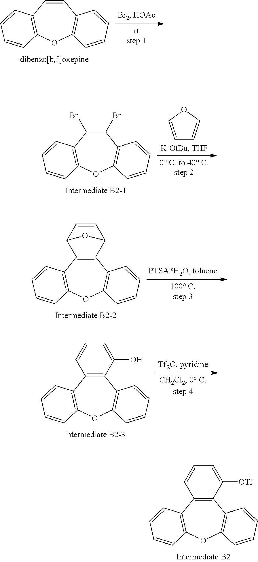


| TABLE 3 |
| The starting materials, including Intermediate B and chlorophenyl |
| boronic acid, used for preparing Intermediates C1 to C3 and their yields and |
| MS data. |
| Intermediate | Chlorophenyl | Yield | Formula | |
| B | boronic acid | Intermediate C | (%) | (FD-MS) |
| Intermediate B1 |
 |
 |
90 | C24H15ClO (354.83) |
| Intermediate B2 |
 |
 |
95 | C24H15ClO (354.83) |
| Intermediate B2 |
 |
 |
93 | C24H15ClO (354.83) |


| TABLE 4 |
| The starting materials, including Intermediate A and B, used for |
| preparing Intermediates C7 and C8 and their yields and MS data. |
| Intermediate | Intermediate | Yield | Mass | |
| B | A | Intermediate C | (%) | (M+) |
| Intermediate B1 | Intermediate A9 |
 |
54.4% | 500.59 (C36H24N2O) |
| Intermediate B1 | Intermediate A13 |
 |
80.6% | 576.68 (C42H28N2O) |


| TABLE 5 |
| The reactants A and B used for preparing the novel compounds and |
| their yields and MS data. |
| Mass(M+) | ||||
| Chemical Structure of | Yield | Theoretical | ||
| Reactant A | Reactant B | Novel Compound | (%) | (found) |
| Intermediate A1 | Intermediate B1 |
 |
85.2% | 563.69 (C42H29NO) |
| Intermediate A1 | Intermediate C1 |
 |
90.1% | 639.78 (C48H33NO) |
| Intermediate A1 | Intermediate C2 |
 |
80.5% | 639.78 (C48H33NO) |
| Intermediate A1 | Intermediate C3 |
 |
88.9% | 639.78 (C48H33NO) |
| Intermediate A7 | Intermediate C6 |
 |
86.3% | 715.88 (C57H37NO) |
| Intermediate A8 | Intermediate B1 |
 |
97.3% | 715.88 (C57H37NO) |
| Intermediate C4 | Intermediate C1 |
 |
94.5% | 729.86 (C54H35NO2) |
| Intermediate C4 | Intermediate B1 |
 |
96.1% | 653.77 (C48H31NO2) |
| Intermediate C5 | Intermediate B1 |
 |
88.5% | 743.84 (C54H33NO3) |
| Intermediate C5 | Intermediate C1 |
 |
91.8% | 819.94 (C60H37NO3) |
| Intermediate A5 | Intermediate B1 |
 |
93.7% | 653.77 (C48H31NO2) |
| Intermediate A5 | Intermediate C1 |
 |
88.3% | 805.96 (C60H39NO2) |
| Intermediate A6 | Intermediate C2 |
 |
84.6% | 729.86 (C54H3NO2) |
| Intermediate A2 | Intermediate B1 |
 |
91.5% | 654.8 (C48H34N2O) |
| Intermediate A3 | Intermediate B1 |
 |
83.3% | 820.97 (C60H40N2O2) |
| Intermediate A4 | Intermediate B1 |
 |
86.9% | 820.97 (C60H40N2O2) |
| Intermediate A4 | Intermediate C1 |
 |
87.9% | 973.16 (C72H48N2O2) |
| Intermediate A2 | Intermediate C1 |
 |
90.3% | 730.89 (C54H38N2O) |
| Intermediate B1 | Intermediate A18 |
 |
92.6% | 652.78 (C48H32N2O) |
| Intermediate C1 | Intermediate A18 |
 |
89.4% | 728.88 (C54H36N2O) |
| Intermediate C2 | Intermediate A18 |
 |
87.6% | 894.07 (C66H43N3O) |
| Intermediate B1 | Intermediate A8 |
 |
89.7% | 741.88 (C54H35N3O) |
| Intermediate C1 | Intermediate A8 |
 |
90.3% | 817.97 (C60H39N3O) |
| Intermediate B1 | Intermediate A16 |
 |
87.9% | 817.97 (C60H39N3O) |
| Intermediate C1 | Intermediate A16 |
 |
92.6% | 894.07 (C66H43N3O) |
| Intermediate B1 | Intermediate A17 |
 |
91.0% | 894.07 (C66H43N3O) |
| Intermediate B1 | Intermediate A19 |
 |
93.7% | 652.78 (C48H32N2O) |
| Intermediate B1 | Intermediate A20 |
 |
90.9% | 728.88 (C54H36N2O) |
| Intermediate C1 | Intermediate A20 |
 |
88.8% | 804.97 (C60H40N2O) |
| Intermediate B1 | Intermediate A12 |
 |
95.0% | 650.76 (C48H30N2O) |
| Intermediate A10 | Intermediate C5 |
 |
92.5% | 742.86 (C54H34N2O2) |
| Intermediate C1 | Intermediate C7 |
 |
87.9% | 818.96 (C60H38N2O2) |
| Intermediate A14 | Intermediate C5 |
 |
93.3% | 818.96 (C60H38N2O2) |
| Intermediate B3 | Intermediate C8 |
 |
82.5% | 895.05 (C66H42N2O2) |
| Intermediate C1 | Intermediate C8 |
 |
88.6% | 895.05 (C66H42N2O2) |
| Intermediate B1 | Intermediate A29 |
 |
90.1% | 653.77 (C48H31NO2) |
| Intermediate C1 | Intermediate A29 |
 |
91.3% | 729.86 (C54H35NO2) |
| Intermediate C2 | Intermediate A29 |
 |
86.3% | 729.86 (C54H35NO2) |
| Intermediate B1 | Intermediate A30 |
 |
88.4% | 742.86 (C54H34N2O2) |
| Intermediate B1 | Intermediate A31 |
 |
94.5% | 743.84 (C54H3.NO3) |
| Intermediate B3 | Intermediate C9 |
 |
94.5% | 743.84 (C54H33NO3) |
| Intermediate B1 | Intermediate A27 |
 |
91.3% | 743.84 (C54H33NO3) |
| Intermediate C1 | Intermediate A32 |
 |
86.5% | 818.96 (C60H38N2O2) |
| TABLE 6 |
| chemical structures of commercial materials for OLED devices. |
 |
HAT |
 |
HI-2 |
 |
HT-1 |
 |
HT-2 |
 |
ET |
 |
Liq |
 |
RH |
 |
GH |
 |
BH |
 |
RD |
 |
GD |
 |
BD-1 |
 |
BD-2 |
 |
NPB |
 |
HT-2′ |
 |
HI-2′ (m-MTDATA) |
| TABLE 7 |
| coating sequence, materials and thickness of the organic layers in red |
| OLED device. |
| Coating | ||||
| Sequence | | Material | Thickness | |
| 1 | HIL-1 | HAT | 100 |
|
| 2 | HIL-2 | HI-2 or novel compound doped with | 2100 Å | |
| 5.0 wt % of |
||||
| 3 | HTL-1 | Commercial HT-1 or novel compound | 100 Å | |
| 4 | HTL-2 | Commercial HT-2 or novel compound | 100 Å | |
| 5 | REL | RH doped with 3.5 wt % of RD | 300 Å | |
| 6 | ETL | ET doped with 35.0 wt % of Liq | 350 |
|
| 7 | | Liq | 15 |
|
| 8 | Cthd | Al | 1500 Å | |
| TABLE 8 |
| coating sequence, materials and thickness of the layers in green OLED |
| device. |
| Coating | ||||
| Sequence | | Material | Thickness | |
| 1 | HIL-1 | HAT | 100 |
|
| 2 | HIL-2 | HI-2 or novel compound doped with | 1300 Å | |
| 5.0 wt % of |
||||
| 3 | HTL-1 | Commercial HT-1 or novel compound | 100 Å | |
| 4 | HTL-2 | Commercial HT-2 or novel compound | 100 Å | |
| 5 | GEL | GH doped with 10.0 wt % of GD | 400 Å | |
| 6 | ETL | ET doped with 35.0 wt % of Liq | 350 |
|
| 7 | | Liq | 15 |
|
| 8 | Cthd | Al | 1500 Å | |
| TABLE 9 |
| coating sequence, materials and thickness of the layers in blue OLED |
| device. |
| Coating | ||||
| Sequence | | Material | Thickness | |
| 1 | HIL-1 | HAT | 100 |
|
| 2 | HIL-2 | HI-2 or novel compound doped with | 750 Å | |
| 5.0 wt % of |
||||
| 3 | HTL-1 | Commercial HT-1 or novel compound | 100 Å | |
| 4 | HTL-2 | Commercial HT-2 or novel compound | 100 Å | |
| 5 | BEL | BH doped with 3.5 wt % of BD-1 or | 250 Å | |
| BD-2 | ||||
| 6 | ETL | ET doped with 35.0 wt % of Liq | 250 |
|
| 7 | | Liq | 15 |
|
| 8 | Cthd | Al | 1500 Å | |
| TABLE 10 |
| materials of HIL-2, HTL-1, and HTL-2, voltage, CIE (x, y) and |
| current efficiency (E) of OLED devices of Examples 1 to 13 and |
| Comparative Examples 1 to 3. |
| Ex- | ||||
| am- | Material |
| ple | HTL- | HTL- | Voltage | E | ||
| No. | HIL-2 | 1 | 2 | (V) | CIE (x, y) | (cd/A) |
| E1 | Compound 24 | HT1 | HT-2 | 5.33 | B(0.136, 0.171) | 10.9 |
| E2 | Compound 25 | HT-1 | HT-2 | 5.27 | B(0.137, 0.163) | 9.59 |
| E3 | Compound 26 | HT-1 | HT-2 | 4.73 | B(0.136, 0.166) | 12.7 |
| E4 | Compound 43 | HT-1 | HT-2 | 6.11 | B(0.136, 0.174) | 8.99 |
| E5 | Compound 19 | HT-1 | HT-2 | 5.73 | B(0.136, 0.176) | 10.7 |
| C1 | m-MTDATA | HT-1 | HT-2 | 6.81 | B(0.14, 0.187) | 4.59 |
| E6 | Compound 24 | HT-1 | HT-2 | 3.29 | G(0.312, 0.640) | 62 |
| E7 | Compound 25 | HT-1 | HT-2 | 4.08 | G(0.312, 0.638) | 67.8 |
| E8 | Compound 26 | HT-1 | HT-2 | 3.71 | G(0.308, 0.641) | 64.3 |
| E9 | Compound 19 | HT-1 | HT-2 | 4.19 | G(0.322, 0.634) | 63 |
| C2 | m-MTDATA | HT-1 | HT-2 | 4.22 | G(0.325, 0.631) | 55.5 |
| E10 | Compound 16 | HT-1 | HT-2 | 4.59 | R(0.659, 0.339) | 24.4 |
| E11 | Compound 25 | HT-1 | HT-2 | 4.85 | R(0.662, 0.336) | 22.1 |
| E12 | Compound 26 | HT-1 | HT-2 | 4.36 | R(0.659, 0.339) | 22.4 |
| E13 | Compound 19 | HT-1 | HT-2 | 4.95 | R(0.661, 0.338) | 22.7 |
| C3 | m-MTDATA | HT-1 | HT-2 | 5.1 | R(0.656, 0.341) | 20.4 |
| TABLE 11 |
| materials of dopant of emission layer, HTL-1, and HTL-2, voltage, |
| CIE (x, y) and current efficiency (E) of OLED devices of |
| Examples 14 to 69 and Comparative Examples 4 to 9. |
| Dopant | |||||
| of | |||||
| emission | Material | Voltage | E |
| Exp | layer | HTL-1 | HTL-2 | (V) | CIE (x, y) | (cd/A) |
| E14 | BD-1 | compound 1 | HT-2 | 4.25 | B(0.136, 0.178) | 13 |
| E15 | BD-1 | compound 2 | HT-2 | 4.34 | B(0.136, 0.188) | 13.2 |
| E16 | BD-1 | compound 9 | HT-2 | 4.6 | B(0.136, 0.181) | 12.4 |
| E17 | BD-1 | compound 15 | HT-2 | 4.47 | B(0.136, 0.173) | 13.3 |
| E18 | BD-1 | compound 12 | HT-2 | 4.4 | B(0.136, 0.171) | 12.1 |
| E19 | BD-1 | compound 27 | HT-2 | 4.33 | B(0.136, 0.178) | 12.7 |
| E20 | BD-1 | compound 28 | HT-2 | 4.52 | B(0.136, 0.184) | 11.6 |
| E21 | BD-1 | compound 29 | HT-2 | 4.29 | B(0.136, 0.171) | 12 |
| E22 | BD-1 | compound 31 | HT-2 | 4.57 | B(0.136, 0.195) | 13 |
| E23 | BD-1 | compound 32 | HT-2 | 4.42 | B(0.136, 0.178) | 13.1 |
| E24 | BD-1 | compound 36 | HT-2 | 4.21 | B(0.136, 0.168) | 12.6 |
| E25 | BD-1 | compound 37 | HT-2 | 4.74 | B(0.137, 0.163) | 11 |
| E26 | BD-1 | compound 39 | HT-2 | 4.41 | B(0.135, 0.181) | 11.1 |
| E27 | BD-1 | compound 42 | HT-2 | 4.65 | B(0.136, 0.177) | 11.3 |
| E28 | BD-2 | compound 38 | HT-2 | 4.53 | B(0.13, 0.155) | 11 |
| E29 | BD-2 | compound 5 | HT-2 | 4.66 | B(0.13, 0.155) | 10.4 |
| E30 | BD-2 | compound 14 | HT-2 | 4.69 | B(0.130, 0.152) | 11.2 |
| E31 | BD-2 | compound 7 | HT-2 | 4.56 | B(0.129, 0.156) | 10.2 |
| E32 | BD-2 | compound 34 | HT-2 | 4.53 | B(0.13, 0.150) | 10.8 |
| C4 | BD-1 | NPB | HT-2 | 4.97 | B(0.129, 0.180) | 10.6 |
| C5 | BD-2 | NPB | HT-2 | 4.77 | B(0.129, 0.160) | 9.5 |
| E33 | GD | compound 1 | HT-2 | 3.36 | G(0.319, 0.637) | 75.9 |
| E34 | GD | compound 2 | HT-2 | 3.29 | G(0.319, 0.636) | 71.4 |
| E35 | GD | compound 14 | HT-2 | 3.33 | G(0.312, 0.639) | 70.5 |
| E36 | GD | compound 7 | HT-2 | 3.63 | G(0.308, 0.640) | 71.0 |
| E37 | GD | compound 8 | HT-2 | 3.46 | G(0.315, 0.638) | 81.7 |
| E38 | GD | compound 10 | HT-2 | 3.59 | G(0.309, 0.639) | 74.5 |
| E39 | GD | compound 9 | HT-2 | 3.59 | G(0.320, 0.636) | 73.7 |
| E40 | GD | compound 15 | HT-2 | 3.50 | G(0.320, 0.636) | 78.8 |
| E41 | GD | compound 17 | HT-2 | 3.18 | G(0.313, 0.639) | 71.3 |
| E42 | GD | compound 11 | HT-2 | 3.55 | G(0.312, 0.640) | 78.0 |
| E43 | GD | compound 27 | HT-2 | 3.42 | G(0.317, 0.638) | 76.3 |
| E44 | GD | compound 28 | HT-2 | 3.10 | G(0.315, 0.638) | 75.5 |
| E45 | GD | compound 29 | HT-2 | 3.30 | G(0.311, 0.640) | 74.3 |
| E46 | GD | compound 31 | HT-2 | 3.24 | G(0.32, 0.636) | 71.6 |
| E47 | GD | compound 33 | HT-2 | 3.12 | G(0.313, 0.639) | 74.0 |
| E48 | GD | compound 34 | HT-2 | 3.49 | G(0.312, 0.640) | 74.0 |
| E49 | GD | compound 36 | HT-2 | 3.26 | G(0.313, 0.639) | 70.6 |
| E50 | GD | compound 37 | HT-2 | 3.29 | G(0.31, 0.640) | 71.3 |
| E51 | GD | compound 40 | HT-2 | 3.50 | G(0.31 0.640) | 70.5 |
| E52 | GD | compound 42 | HT-2 | 3.39 | G(0.312, 0.640) | 74.3 |
| C6 | GD | NPB | HT-2 | 3.68 | G(0.317, 0.637) | 70.1 |
| C7 | GD | HT-1 | HT-2 | 5.64 | G(0.318, 0.637) | 69.4 |
| E53 | RD | compound 1 | HT-2 | 3.47 | R(0.662, 0.337) | 22.5 |
| E54 | RD | compound 2 | HT-2 | 3.36 | R(0.660, 0.339) | 23.8 |
| E55 | RD | compound 14 | HT-2 | 3.30 | R(0.661, 0.338) | 23.1 |
| E56 | RD | compound 7 | HT-2 | 3.58 | R(0.658, 0.340) | 24.0 |
| E57 | RD | compound 10 | HT-2 | 3.56 | R(0.659, 0.339) | 23.6 |
| E58 | RD | compound 9 | HT-2 | 3.63 | R(0.659, 0.339) | 24.7 |
| E59 | RD | compound 17 | HT-2 | 3.29 | R(0.662, 0.337) | 20.9 |
| E60 | RD | compound 11 | HT-2 | 3.61 | R(0.660, 0.339) | 22.8 |
| E61 | RD | compound 12 | HT-2 | 3.49 | R(0.661, 0.338) | 23.1 |
| E62 | RD | compound 27 | HT-2 | 3.58 | R(0.662, 0.337) | 23.4 |
| E63 | RD | compound 28 | HT-2 | 3.32 | R(0.659, 0.340) | 23.7 |
| E64 | RD | compound 29 | HT-2 | 3.39 | R(0.66, 0.339) | 24.0 |
| E65 | RD | compound 31 | HT-2 | 3.38 | R(0.663, 0.335) | 23.5 |
| E66 | RD | compound 33 | HT-2 | 3.25 | R(0.659, 0.340) | 24.1 |
| E67 | RD | compound 36 | HT-2 | 3.35 | R(0.659, 0.340) | 22.9 |
| E68 | RD | compound 37 | HT-2 | 3.36 | R(0.658, 0.340) | 23.0 |
| E69 | RD | compound 42 | HT-2 | 3.55 | R(0.661, 0.338) | 25.2 |
| C8 | RD | NPB | HT-2 | 3.67 | R(0.661, 0.330) | 21.3 |
| C9 | RD | HT-1 | HT-2 | 3.69 | R(0.667, 0.332) | 20.7 |
| TABLE 12 |
| materials of HTL-1 and HTL-2, voltage, CIE (x, y) and current |
| efficiency (E) of OLED devices of Examples 70 to 81 and |
| Comparative Examples 10 to 15. |
| Material | Voltage | E |
| Exp | HTL-1 | HTL-2 | (V) | CIE (x, y) | (cd/A) |
| E70 | HT-1 | compound 1 | 4.12 | B(0.135, 0.165) | 11.4 |
| E71 | HT-1 | compound 3 | 4.11 | B(0.128, 0.156) | 11.4 |
| E72 | HT-1 | compound 13 | 4.08 | B(0.13, 0.144) | 10.9 |
| C10 | HT-1 | HT-2′ | 4.49 | B(0.129, 0.169) | 9.1 |
| C11 | HT-1 | HT-2 | 4.14 | B(0.129, 0.151) | 10.4 |
| E73 | HT-1 | compound 1 | 3.16 | G(0.317, 0.638) | 75.0 |
| E74 | HT-1 | compound 3 | 3.41 | G(0.318, 0.636) | 70.0 |
| E75 | HT-1 | compound 6 | 3.51 | G(0.315, 0.637) | 71.8 |
| E76 | HT-1 | compound 13 | 3.42 | G(0.314, 0.632) | 72.4 |
| C12 | HT-1 | HT-2′ | 3.82 | G(0.312, 0.639) | 48.6 |
| C13 | HT-1 | HT-2 | 5.64 | G(0.318, 0.637) | 69.4 |
| E77 | HT-1 | compound 1 | 3.36 | R(0.663, 0.336) | 21.3 |
| E78 | HT-1 | compound 3 | 3.51 | R(0.659, 0.339) | 21.4 |
| E79 | HT-1 | compound 11 | 3.24 | R(0.661, 0.338) | 22.7 |
| E80 | HT-1 | compound 13 | 3.36 | R(0.657, 0.342) | 24.9 |
| E81 | HT-1 | compound 41 | 3.6 | R(0.655, 0.343) | 28.4 |
| C14 | HT-1 | HT-2 | 3.69 | R(0.667, 0.332) | 20.7 |
| C15 | HT-1 | HT-2′ | 6.43 | R(0.635, 0.354) | 6.88 |
Claims (20)


Priority Applications (1)
| Application Number | Priority Date | Filing Date | Title |
|---|---|---|---|
| US15/679,379 US10396292B2 (en) | 2016-08-19 | 2017-08-17 | Compound and organic electronic device using the same |
Applications Claiming Priority (5)
| Application Number | Priority Date | Filing Date | Title |
|---|---|---|---|
| US201662377024P | 2016-08-19 | 2016-08-19 | |
| US201662377014P | 2016-08-19 | 2016-08-19 | |
| US201662377029P | 2016-08-19 | 2016-08-19 | |
| US201662377740P | 2016-08-22 | 2016-08-22 | |
| US15/679,379 US10396292B2 (en) | 2016-08-19 | 2017-08-17 | Compound and organic electronic device using the same |
Publications (2)
| Publication Number | Publication Date |
|---|---|
| US20180053899A1 US20180053899A1 (en) | 2018-02-22 |
| US10396292B2 true US10396292B2 (en) | 2019-08-27 |
Family
ID=61192193
Family Applications (1)
| Application Number | Title | Priority Date | Filing Date |
|---|---|---|---|
| US15/679,379 Expired - Fee Related US10396292B2 (en) | 2016-08-19 | 2017-08-17 | Compound and organic electronic device using the same |
Country Status (5)
| Country | Link |
|---|---|
| US (1) | US10396292B2 (en) |
| JP (1) | JP6498245B2 (en) |
| KR (1) | KR101965763B1 (en) |
| CN (1) | CN107759559B (en) |
| TW (1) | TWI641598B (en) |
Cited By (1)
| Publication number | Priority date | Publication date | Assignee | Title |
|---|---|---|---|---|
| US11706973B2 (en) | 2017-06-20 | 2023-07-18 | Samsung Display Co., Ltd. | Condensed cyclic compound and organic light-emitting device including the same |
Families Citing this family (3)
| Publication number | Priority date | Publication date | Assignee | Title |
|---|---|---|---|---|
| US11744145B2 (en) * | 2018-11-05 | 2023-08-29 | Lg Display Co., Ltd. | Organic compound and organic electroluminescent device comprising the same |
| CN115433168B (en) * | 2021-06-03 | 2024-03-29 | 宁波卢米蓝新材料有限公司 | Heterocyclic compound, organic electroluminescent material and organic electroluminescent device using same |
| KR20230029441A (en) * | 2021-08-24 | 2023-03-03 | 엘티소재주식회사 | Heterocyclic compound and organic light emitting device comprising the same |
Citations (6)
| Publication number | Priority date | Publication date | Assignee | Title |
|---|---|---|---|---|
| CN105793246A (en) | 2013-12-06 | 2016-07-20 | 默克专利有限公司 | Substituted oxepines |
| US20170179401A1 (en) * | 2015-12-22 | 2017-06-22 | Samsung Display Co., Ltd. | Organic light-emitting device |
| US20170179397A1 (en) * | 2015-12-22 | 2017-06-22 | Samsung Display Co., Ltd. | Organic light-emitting device |
| KR20170074649A (en) | 2015-12-22 | 2017-06-30 | 주식회사 두산 | Organic compounds and organic electro luminescence device comprising the same |
| US20170279050A1 (en) * | 2016-03-24 | 2017-09-28 | Nichem Fine Technology Co., Ltd. | Compound and organic electronic device using the same |
| US20180366647A1 (en) * | 2017-06-20 | 2018-12-20 | Samsung Display Co., Ltd. | Condensed cyclic compound and organic light-emitting device including the same |
Family Cites Families (3)
| Publication number | Priority date | Publication date | Assignee | Title |
|---|---|---|---|---|
| TW200505435A (en) * | 2003-01-29 | 2005-02-16 | Novartis Ag | Treatment of ocular disorders |
| KR20150021861A (en) * | 2013-08-21 | 2015-03-03 | 최돈수 | Light-emitting material for organic electroluminescent device, organic electroluminescent device using same, and material for organic electroluminescent device |
| KR20150103968A (en) * | 2014-03-04 | 2015-09-14 | 주식회사 두산 | Organic compounds and organic electro luminescence device comprising the same |
-
2017
- 2017-08-17 KR KR1020170104296A patent/KR101965763B1/en active IP Right Grant
- 2017-08-17 TW TW106127860A patent/TWI641598B/en not_active IP Right Cessation
- 2017-08-17 JP JP2017157429A patent/JP6498245B2/en not_active Expired - Fee Related
- 2017-08-17 US US15/679,379 patent/US10396292B2/en not_active Expired - Fee Related
- 2017-08-18 CN CN201710711255.2A patent/CN107759559B/en active Active
Patent Citations (6)
| Publication number | Priority date | Publication date | Assignee | Title |
|---|---|---|---|---|
| CN105793246A (en) | 2013-12-06 | 2016-07-20 | 默克专利有限公司 | Substituted oxepines |
| US20170179401A1 (en) * | 2015-12-22 | 2017-06-22 | Samsung Display Co., Ltd. | Organic light-emitting device |
| US20170179397A1 (en) * | 2015-12-22 | 2017-06-22 | Samsung Display Co., Ltd. | Organic light-emitting device |
| KR20170074649A (en) | 2015-12-22 | 2017-06-30 | 주식회사 두산 | Organic compounds and organic electro luminescence device comprising the same |
| US20170279050A1 (en) * | 2016-03-24 | 2017-09-28 | Nichem Fine Technology Co., Ltd. | Compound and organic electronic device using the same |
| US20180366647A1 (en) * | 2017-06-20 | 2018-12-20 | Samsung Display Co., Ltd. | Condensed cyclic compound and organic light-emitting device including the same |
Non-Patent Citations (1)
| Title |
|---|
| English translation of Japanese Office Action for Appl. No. 2017-157429 dated Aug. 1, 2018. |
Cited By (1)
| Publication number | Priority date | Publication date | Assignee | Title |
|---|---|---|---|---|
| US11706973B2 (en) | 2017-06-20 | 2023-07-18 | Samsung Display Co., Ltd. | Condensed cyclic compound and organic light-emitting device including the same |
Also Published As
| Publication number | Publication date |
|---|---|
| KR101965763B1 (en) | 2019-04-04 |
| CN107759559B (en) | 2021-03-02 |
| CN107759559A (en) | 2018-03-06 |
| JP6498245B2 (en) | 2019-04-10 |
| US20180053899A1 (en) | 2018-02-22 |
| JP2018048111A (en) | 2018-03-29 |
| TW201806937A (en) | 2018-03-01 |
| TWI641598B (en) | 2018-11-21 |
| KR20180020911A (en) | 2018-02-28 |
Similar Documents
| Publication | Publication Date | Title |
|---|---|---|
| US10312459B2 (en) | Compound and organic electronic device using the same | |
| US20180093962A1 (en) | Novel organic compound and oranic light-emitting diode comprising same background of the invention | |
| US10672993B2 (en) | Nitrogen-containing polycyclic compound and organic light emitting element using same | |
| US10745362B2 (en) | Heterocyclic compound and organic light emitting device comprising same | |
| US8906521B2 (en) | Organic electroluminescent device having triptycene derivative material | |
| US10756277B2 (en) | Organic compound and organic electroluminescent device comprising the same | |
| KR101218029B1 (en) | Triphenylene-based compounds that substitute aryl amine compounds and organic electroluminescent device comprising same | |
| US10529928B2 (en) | Compound and organic electronic device using the same | |
| US11917909B2 (en) | Organic compound and organic electroluminescence device using the same | |
| US20190140177A1 (en) | Amine-substituted naphthalene derivatives and organic light emitting diodes including the same | |
| US10396292B2 (en) | Compound and organic electronic device using the same | |
| US20170141322A1 (en) | Novel amine compounds for organic light-emitting diode and organic light-emitting diode including the same | |
| CN110088110B (en) | Novel compound and organic light-emitting element comprising same | |
| KR20150047858A (en) | Organic compounds and organic electro luminescence device comprising the same | |
| US11667622B2 (en) | Organic light emitting compound and organic electroluminescence device using same | |
| KR20200090597A (en) | Organic Compound for organic light emitting diode and an organic light emitting diode including the same with long life | |
| KR20200090620A (en) | Organic Compound for organic light emitting diode and an organic light emitting diode including the same with long life | |
| US20190372016A1 (en) | Compound and organic electronic device using the same | |
| US9991449B2 (en) | Anthracene derivatives for organic light-emitting diode and organic light-emitting diode including the same | |
| US10510962B2 (en) | Compound and organic electronic device using the same | |
| US11858906B2 (en) | Amine compound and high-efficiency organic light-emitting diode including same | |
| US10454039B2 (en) | Compound and organic electronic device using the same | |
| US10494359B2 (en) | Compound and organic electronic device using the same | |
| KR101759439B1 (en) | Organic compounds and organic electro luminescence device comprising the same | |
| US20200274070A1 (en) | Compound and organic electronic device using the same |
Legal Events
| Date | Code | Title | Description |
|---|---|---|---|
| AS | Assignment |
Owner name: NICHEM FINE TECHNOLOGY CO., LTD., TAIWAN Free format text: ASSIGNMENT OF ASSIGNORS INTEREST;ASSIGNORS:WU, HUI-LING;LIAO, LIANG-DI;SHIEH, SHWU-JU;AND OTHERS;REEL/FRAME:043333/0138 Effective date: 20170814 |
|
| STPP | Information on status: patent application and granting procedure in general |
Free format text: DOCKETED NEW CASE - READY FOR EXAMINATION |
|
| AS | Assignment |
Owner name: SHANGHAI NICHEM FINE CHEMICAL CO., LTD., CHINA Free format text: ASSIGNMENT OF ASSIGNORS INTEREST;ASSIGNOR:NICHEM FINE TECHNOLOGY CO., LTD.;REEL/FRAME:049039/0347 Effective date: 20190425 |
|
| STPP | Information on status: patent application and granting procedure in general |
Free format text: NOTICE OF ALLOWANCE MAILED -- APPLICATION RECEIVED IN OFFICE OF PUBLICATIONS |
|
| STPP | Information on status: patent application and granting procedure in general |
Free format text: PUBLICATIONS -- ISSUE FEE PAYMENT RECEIVED |
|
| STPP | Information on status: patent application and granting procedure in general |
Free format text: PUBLICATIONS -- ISSUE FEE PAYMENT VERIFIED |
|
| STCF | Information on status: patent grant |
Free format text: PATENTED CASE |
|
| FEPP | Fee payment procedure |
Free format text: MAINTENANCE FEE REMINDER MAILED (ORIGINAL EVENT CODE: REM.); ENTITY STATUS OF PATENT OWNER: SMALL ENTITY |
|
| LAPS | Lapse for failure to pay maintenance fees |
Free format text: PATENT EXPIRED FOR FAILURE TO PAY MAINTENANCE FEES (ORIGINAL EVENT CODE: EXP.); ENTITY STATUS OF PATENT OWNER: SMALL ENTITY |
|
| STCH | Information on status: patent discontinuation |
Free format text: PATENT EXPIRED DUE TO NONPAYMENT OF MAINTENANCE FEES UNDER 37 CFR 1.362 |
|
| FP | Lapsed due to failure to pay maintenance fee |
Effective date: 20230827 |