US10354969B2 - Substrate structure, semiconductor package including the same, and method for manufacturing the same - Google Patents
Substrate structure, semiconductor package including the same, and method for manufacturing the same Download PDFInfo
- Publication number
- US10354969B2 US10354969B2 US15/665,289 US201715665289A US10354969B2 US 10354969 B2 US10354969 B2 US 10354969B2 US 201715665289 A US201715665289 A US 201715665289A US 10354969 B2 US10354969 B2 US 10354969B2
- Authority
- US
- United States
- Prior art keywords
- layer
- conductive structure
- protective layer
- conductive
- circuit
- Prior art date
- Legal status (The legal status is an assumption and is not a legal conclusion. Google has not performed a legal analysis and makes no representation as to the accuracy of the status listed.)
- Active
Links
Images


Classifications
-
- H—ELECTRICITY
- H10—SEMICONDUCTOR DEVICES; ELECTRIC SOLID-STATE DEVICES NOT OTHERWISE PROVIDED FOR
- H10W—GENERIC PACKAGES, INTERCONNECTIONS, CONNECTORS OR OTHER CONSTRUCTIONAL DETAILS OF DEVICES COVERED BY CLASS H10
- H10W72/00—Interconnections or connectors in packages
- H10W72/20—Bump connectors, e.g. solder bumps or copper pillars; Dummy bumps; Thermal bumps
-
- H—ELECTRICITY
- H10—SEMICONDUCTOR DEVICES; ELECTRIC SOLID-STATE DEVICES NOT OTHERWISE PROVIDED FOR
- H10W—GENERIC PACKAGES, INTERCONNECTIONS, CONNECTORS OR OTHER CONSTRUCTIONAL DETAILS OF DEVICES COVERED BY CLASS H10
- H10W70/00—Package substrates; Interposers; Redistribution layers [RDL]
- H10W70/20—Conductive package substrates serving as an interconnection, e.g. metal plates
-
- H01L24/14—
-
- H01L21/4846—
-
- H01L24/11—
-
- H—ELECTRICITY
- H10—SEMICONDUCTOR DEVICES; ELECTRIC SOLID-STATE DEVICES NOT OTHERWISE PROVIDED FOR
- H10W—GENERIC PACKAGES, INTERCONNECTIONS, CONNECTORS OR OTHER CONSTRUCTIONAL DETAILS OF DEVICES COVERED BY CLASS H10
- H10W70/00—Package substrates; Interposers; Redistribution layers [RDL]
- H10W70/01—Manufacture or treatment
- H10W70/04—Manufacture or treatment of leadframes
-
- H—ELECTRICITY
- H10—SEMICONDUCTOR DEVICES; ELECTRIC SOLID-STATE DEVICES NOT OTHERWISE PROVIDED FOR
- H10W—GENERIC PACKAGES, INTERCONNECTIONS, CONNECTORS OR OTHER CONSTRUCTIONAL DETAILS OF DEVICES COVERED BY CLASS H10
- H10W70/00—Package substrates; Interposers; Redistribution layers [RDL]
- H10W70/01—Manufacture or treatment
- H10W70/05—Manufacture or treatment of insulating or insulated package substrates, or of interposers, or of redistribution layers
-
- H—ELECTRICITY
- H10—SEMICONDUCTOR DEVICES; ELECTRIC SOLID-STATE DEVICES NOT OTHERWISE PROVIDED FOR
- H10W—GENERIC PACKAGES, INTERCONNECTIONS, CONNECTORS OR OTHER CONSTRUCTIONAL DETAILS OF DEVICES COVERED BY CLASS H10
- H10W70/00—Package substrates; Interposers; Redistribution layers [RDL]
- H10W70/40—Leadframes
- H10W70/451—Multilayered leadframes
-
- H—ELECTRICITY
- H10—SEMICONDUCTOR DEVICES; ELECTRIC SOLID-STATE DEVICES NOT OTHERWISE PROVIDED FOR
- H10W—GENERIC PACKAGES, INTERCONNECTIONS, CONNECTORS OR OTHER CONSTRUCTIONAL DETAILS OF DEVICES COVERED BY CLASS H10
- H10W72/00—Interconnections or connectors in packages
- H10W72/01—Manufacture or treatment
- H10W72/012—Manufacture or treatment of bump connectors, dummy bumps or thermal bumps
-
- H—ELECTRICITY
- H10—SEMICONDUCTOR DEVICES; ELECTRIC SOLID-STATE DEVICES NOT OTHERWISE PROVIDED FOR
- H10W—GENERIC PACKAGES, INTERCONNECTIONS, CONNECTORS OR OTHER CONSTRUCTIONAL DETAILS OF DEVICES COVERED BY CLASS H10
- H10W74/00—Encapsulations, e.g. protective coatings
- H10W74/10—Encapsulations, e.g. protective coatings characterised by their shape or disposition
- H10W74/111—Encapsulations, e.g. protective coatings characterised by their shape or disposition the semiconductor body being completely enclosed
- H10W74/114—Encapsulations, e.g. protective coatings characterised by their shape or disposition the semiconductor body being completely enclosed by a substrate and the encapsulations
-
- H—ELECTRICITY
- H10—SEMICONDUCTOR DEVICES; ELECTRIC SOLID-STATE DEVICES NOT OTHERWISE PROVIDED FOR
- H10W—GENERIC PACKAGES, INTERCONNECTIONS, CONNECTORS OR OTHER CONSTRUCTIONAL DETAILS OF DEVICES COVERED BY CLASS H10
- H10W90/00—Package configurations
- H10W90/701—Package configurations characterised by the relative positions of pads or connectors relative to package parts
-
- H01L2224/131—
-
- H01L2224/16235—
-
- H01L2224/16238—
-
- H01L24/13—
-
- H01L24/16—
-
- H01L2924/00014—
-
- H01L2924/014—
-
- H01L2924/15313—
-
- H—ELECTRICITY
- H10—SEMICONDUCTOR DEVICES; ELECTRIC SOLID-STATE DEVICES NOT OTHERWISE PROVIDED FOR
- H10W—GENERIC PACKAGES, INTERCONNECTIONS, CONNECTORS OR OTHER CONSTRUCTIONAL DETAILS OF DEVICES COVERED BY CLASS H10
- H10W70/00—Package substrates; Interposers; Redistribution layers [RDL]
- H10W70/60—Insulating or insulated package substrates; Interposers; Redistribution layers
- H10W70/67—Insulating or insulated package substrates; Interposers; Redistribution layers characterised by their insulating layers or insulating parts
- H10W70/68—Shapes or dispositions thereof
- H10W70/685—Shapes or dispositions thereof comprising multiple insulating layers
-
- H—ELECTRICITY
- H10—SEMICONDUCTOR DEVICES; ELECTRIC SOLID-STATE DEVICES NOT OTHERWISE PROVIDED FOR
- H10W—GENERIC PACKAGES, INTERCONNECTIONS, CONNECTORS OR OTHER CONSTRUCTIONAL DETAILS OF DEVICES COVERED BY CLASS H10
- H10W72/00—Interconnections or connectors in packages
- H10W72/20—Bump connectors, e.g. solder bumps or copper pillars; Dummy bumps; Thermal bumps
- H10W72/251—Materials
- H10W72/252—Materials comprising solid metals or solid metalloids, e.g. PbSn, Ag or Cu
-
- H—ELECTRICITY
- H10—SEMICONDUCTOR DEVICES; ELECTRIC SOLID-STATE DEVICES NOT OTHERWISE PROVIDED FOR
- H10W—GENERIC PACKAGES, INTERCONNECTIONS, CONNECTORS OR OTHER CONSTRUCTIONAL DETAILS OF DEVICES COVERED BY CLASS H10
- H10W90/00—Package configurations
- H10W90/701—Package configurations characterised by the relative positions of pads or connectors relative to package parts
- H10W90/721—Package configurations characterised by the relative positions of pads or connectors relative to package parts of bump connectors
- H10W90/724—Package configurations characterised by the relative positions of pads or connectors relative to package parts of bump connectors between a chip and a stacked insulating package substrate, interposer or RDL
Definitions
- the present disclosure relates to a substrate structure, a semiconductor package and a manufacturing method, and to a substrate structure including an embedded trace substrate (ETS), a semiconductor package including the substrate structure, and a method for manufacturing the substrate structure.
- ETS embedded trace substrate
- Semiconductor chips may be integrated with a large number of electronic components to achieve strong electrical performance. Accordingly, the semiconductor chips are provided with a large number of input/output (I/O) connections. To implement semiconductor packages that use semiconductor chips with a large number of I/O connections, the semiconductor chips and the semiconductor packages may correspondingly be made large. Thus, a cost of manufacture may correspondingly be large. Alternatively, to keep semiconductor packages small while implementing semiconductor chips with a large number of I/O connections, a bonding pad density of semiconductor substrates used for carrying the semiconductor chips may correspondingly be made large. However, in such implementations, formation of bridges between solder on the bonding pads may be an issue of concern.
- a substrate structure includes a dielectric layer, a first circuit layer, at least one conductive structure and a first protective layer.
- the first circuit layer is disposed adjacent to a first surface of the dielectric layer.
- the conductive structure includes a first portion and a second portion. The first portion is disposed on the first circuit layer.
- the first protective layer is disposed on the dielectric layer and contacts at least a portion of a sidewall of the first portion of the conductive structure.
- the first circuit layer and the conductive structure are integrally formed.
- a semiconductor package includes a substrate structure, a semiconductor die and an encapsulant.
- the substrate structure includes a dielectric layer, a first circuit layer, at least one conductive structure and a first protective layer.
- the first circuit layer is disposed adjacent to a first surface of the dielectric layer.
- the conductive structure includes a first portion and a second portion. The first portion is disposed on the first circuit layer.
- the first protective layer is disposed on the dielectric layer and contacts at least a portion of a sidewall of the first portion of the conductive structure.
- the first circuit layer and the conductive structure are integrally formed.
- the semiconductor die is disposed on the substrate structure and is electrically connected to the second portion of the conductive structure.
- the encapsulant covers the semiconductor die and the substrate structure.
- a method for manufacturing a substrate structure includes providing a carrier, and forming a first photoresist, a first protective layer and a second photoresist on the carrier, wherein the first photoresist defines at least one first opening, the first protective layer defines at least one second opening communicating with the first opening of the first photoresist, the second photoresist defines a plurality of circuit openings, and at least one of the circuit openings communicates with the second opening of the first protective layer.
- the method further includes integrally forming a second portion of a conductive structure, a first portion of the conductive structure and a first circuit layer respectively in the first opening of the first photoresist, the second opening of the first protective layer and the circuit openings of the second photoresist, and removing the carrier and the first photoresist to expose an upper surface and a sidewall of the second portion of the conductive structure.
- FIG. 1 illustrates a cross-sectional view of some embodiments of a substrate structure according to an aspect of the present disclosure.
- FIG. 2 illustrates a cross-sectional view of some embodiments of a substrate structure according to an aspect of the present disclosure.
- FIG. 3 illustrates a cross-sectional view of some embodiments of a substrate structure according to an aspect of the present disclosure.
- FIG. 4 illustrates a cross-sectional view of some embodiments of a substrate structure according to an aspect of the present disclosure.
- FIG. 5 illustrates a cross-sectional view of some embodiments of a substrate structure according to an aspect of the present disclosure.
- FIG. 6 illustrates a cross-sectional view of some embodiments of a semiconductor package according to an aspect of the present disclosure.
- FIG. 7 illustrates one or more stages of an example of a method for manufacturing a substrate structure according to some embodiments of the present disclosure.
- FIG. 8 illustrates one or more stages of an example of a method for manufacturing a substrate structure according to some embodiments of the present disclosure.
- FIG. 9 illustrates one or more stages of an example of a method for manufacturing a substrate structure according to some embodiments of the present disclosure.
- FIG. 10 illustrates one or more stages of an example of a method for manufacturing a substrate structure according to some embodiments of the present disclosure.
- FIG. 11 illustrates one or more stages of an example of a method for manufacturing a substrate structure according to some embodiments of the present disclosure.
- FIG. 12 illustrates one or more stages of an example of a method for manufacturing a substrate structure according to some embodiments of the present disclosure.
- FIG. 13 illustrates one or more stages of an example of a method for manufacturing a substrate structure according to some embodiments of the present disclosure.
- FIG. 14 illustrates one or more stages of an example of a method for manufacturing a substrate structure according to some embodiments of the present disclosure.
- FIG. 15 illustrates one or more stages of an example of a method for manufacturing a substrate structure according to some embodiments of the present disclosure.
- FIG. 16 illustrates one or more stages of an example of a method for manufacturing a substrate structure according to some embodiments of the present disclosure.
- FIG. 17 illustrates one or more stages of an example of a method for manufacturing a substrate structure according to some embodiments of the present disclosure.
- FIG. 18 illustrates one or more stages of an example of a method for manufacturing a substrate structure according to some embodiments of the present disclosure.
- FIG. 19 illustrates one or more stages of an example of a method for manufacturing a substrate structure according to some embodiments of the present disclosure.
- FIG. 20 illustrates one or more stages of an example of a method for manufacturing a substrate structure according to some embodiments of the present disclosure.
- FIG. 21 illustrates one or more stages of an example of a method for manufacturing a substrate structure according to some embodiments of the present disclosure.
- FIG. 22 illustrates one or more stages of an example of a method for manufacturing a substrate structure according to some embodiments of the present disclosure.
- FIG. 23 illustrates one or more stages of an example of a method for manufacturing a substrate structure according to some embodiments of the present disclosure.
- FIG. 24 illustrates one or more stages of an example of a method for manufacturing a substrate structure according to some embodiments of the present disclosure.
- FIG. 25 illustrates one or more stages of an example of a method for manufacturing a substrate structure according to some embodiments of the present disclosure.
- FIG. 26 illustrates one or more stages of an example of a method for manufacturing a substrate structure according to some embodiments of the present disclosure.
- FIG. 27 illustrates one or more stages of an example of a method for manufacturing a substrate structure according to some embodiments of the present disclosure.
- FIG. 28 illustrates one or more stages of an example of a method for manufacturing a substrate structure according to some embodiments of the present disclosure.
- FIG. 29 illustrates one or more stages of an example of a method for manufacturing a substrate structure according to some embodiments of the present disclosure.
- FIG. 30 illustrates one or more stages of an example of a method for manufacturing a substrate structure according to some embodiments of the present disclosure.
- FIG. 31 illustrates one or more stages of an example of a method for manufacturing a substrate structure according to some embodiments of the present disclosure.
- FIG. 32 illustrates one or more stages of an example of a method for manufacturing a substrate structure according to some embodiments of the present disclosure.
- first and second features are formed or disposed in direct contact
- additional features may be formed or disposed between the first and second features, such that the first and second features may not be in direct contact
- present disclosure may repeat reference numerals and/or letters in the various examples. This repetition is for the purpose of simplicity and clarity and does not in itself dictate a relationship between the various embodiments and/or configurations discussed.
- At least some embodiments of the present disclosure disclose a substrate structure including a conductive structure having a first portion and a second portion, a first protective layer contacting at least a part of a sidewall of the first portion of the conductive structure, and a first circuit layer integrally formed with the conductive structure. At least some embodiments of the present disclosure further disclose a semiconductor package including the substrate structure, and techniques for manufacturing the substrate structure.
- a substrate structure may be manufactured by the following comparative process. Firstly, a dielectric structure is provided with a circuit layer embedded therein.
- the circuit layer may include a plurality of bump pads exposed from a surface of the dielectric structure.
- a plurality of pillars are formed on respective ones of the bump pads of the circuit layer by electroplating.
- a protective layer is formed to cover the pillars and the circuit layer.
- a portion of the protective layer is removed by developing or etching to expose a portion of each pillar.
- the pillar can be connected to the semiconductor chip so as to reduce a volume of solder (or provide for omission of solder) used for electrically connecting the circuit layer to the semiconductor chip, which provides for a low risk of solder bridge formation.
- the present disclosure provides for a substrate structure including a conductive structure having a first portion and a second portion, a first protective layer contacting at least a part of a sidewall of the first portion of the conductive structure, and a first circuit layer integrally formed with the conductive structure.
- the second portion of the conductive structure can be used as a pillar, which is provided with a sufficient height for external connection, such as connection with a semiconductor chip or a semiconductor die. Additionally, since the first portion and the second portion of the conductive structure are integrally formed with the first circuit layer, cracks and peeling between the conductive structure and the first circuit layer can be reduced.
- FIG. 1 illustrates a cross-sectional view of some embodiments of a substrate structure 1 according to an aspect of the present disclosure.
- the substrate structure 1 may be an ETS, and includes a dielectric layer 3 , a first circuit layer 4 , a first protective layer 6 , at least one conductive structure 5 , a second circuit layer 8 , and a second protective layer 9 .
- the dielectric layer 3 has a first surface 31 and a second surface 32 opposite to the first surface 31 .
- the dielectric layer 3 may include an insulating material or a dielectric material, such as, for example, polypropylene (PP). It is noted that the dielectric layer 3 may include, or be formed from, other material such as a cured photoimageable dielectric (PID) material such as epoxy or polyimide (PI) including photoinitiators.
- PID cured photoimageable dielectric
- PI polyimide
- the first circuit layer 4 is disposed adjacent to the first surface 31 of the dielectric layer 3 .
- the first circuit layer 4 is embedded in the dielectric layer 3 and exposed from the first surface 31 of the dielectric layer 3 .
- the first circuit layer 4 is a patterned conductive circuit layer.
- the first circuit layer 4 includes at least one trace 42 and at least one bump pad 44 .
- the bump pad 44 is connected to the trace 42 .
- the trace 42 and the bump pad 44 can be formed or disposed concurrently.
- the bump pad 44 has an upper surface 441 substantially coplanar with the first surface 31 of the dielectric layer 3 .
- the trace 42 and the bump pad 44 of the first circuit layer 4 may be composed of, or may include, a conductive material 46 and a seed layer 48 .
- the conductive material 46 may include a conductive metal, such as copper, or another metal or combination of metals, and may be formed or disposed by electroplating.
- the seed layer 48 may include, for example, titanium and/or copper, and may be formed or disposed by sputtering.
- the first protective layer 6 is disposed on the first surface 31 of the dielectric layer 3 .
- the first protective layer 6 has a first surface 61 and a second surface 62 opposite to the first surface 61 .
- the second surface 62 of the first protective layer 6 is disposed on (e.g. is in contact with) the first surface 31 of the dielectric layer 3 .
- the first protective layer 6 may cover at least a portion of the first circuit layer 4 .
- the first protective layer 6 covers the trace 42 and a portion of the bump pad 44 .
- the first protective layer 6 defines at least one second opening 60 extending through the first protective layer 6 .
- the position of the second opening 60 corresponds to the position of the bump pad 44 of the first circuit layer 4 (e.g. the second opening 60 exposes at least a portion of the bump pad 44 ).
- the first protective layer 6 may include a solder resist material, such as, for example, benzocyclobutene (BCB) or polyimide.
- BCB benzocyclobuten
- the conductive structure 5 is disposed on the first circuit layer 4 .
- the conductive structure 5 includes a first portion 51 and a second portion 52 .
- a minimum width W 1 of the first portion 51 of the conductive structure 5 is greater than a minimum width W 2 of the second portion 52 of the conductive structure 5 .
- the first portion 51 is disposed on the bump pad 44 of the first circuit layer 4 .
- the first portion 51 has an upper surface 511 and a sidewall 514 .
- the first portion 51 is disposed in the second opening 60 of the first protective layer 6 so that the first protective layer 6 contacts at least a portion of the sidewall 514 of the first portion 51 .
- the upper surface 511 of the first portion 51 is substantially coplanar with the first surface 61 of the first protective layer 6 .
- a thickness of the first portion 51 may be substantially equal to a thickness of the first protective layer 6 .
- the upper surface 61 of the first protective layer 6 is not at the same level with the upper surface 511 of the first portion 51 (e.g. as shown in FIG. 2 and FIG. 3 ).
- the second portion 52 is disposed on the first portion 51 and protrudes from the first surface 61 of the first protective layer 6 .
- the second portion 52 has an upper surface 521 and a sidewall 522 .
- the first portion 51 and the second portion 52 of the conductive structure 5 are integrally formed.
- the first conductive structure 5 including the first portion 51 and the second portion 52 , is integrally formed with the first circuit layer 4 .
- the bump pad 44 of the first circuit layer 4 and the first portion 51 and the second portion 52 of the conductive structure 5 are a monolithic structure.
- the conductive structure 5 may also include the seed layer 48 and the conductive material 46 .
- the first portion 51 of the conductive structure 5 includes the seed layer 48 and the conductive material 46 .
- the seed layer 48 is disposed between the conductive material 46 and the first protective layer 6 .
- the first portion 51 includes a portion (e.g. a top portion 481 ) of the seed layer 48 disposed adjacent to the first surface 61 of the first protective layer 6 .
- the upper surface 511 of the first portion 51 is a surface of the top portion 481 of the seed layer 48 .
- the second portion 52 also includes the seed layer 48 and the material 46 .
- the seed layer 48 is exposed and surrounds the conductive material 46 .
- the upper surface 521 and the sidewall 522 of the second portion 52 are surfaces of the seed layer 48 .
- the substrate structure 1 may include a plurality of conductive structures 5 .
- Each of the second portions 52 of the conductive structures 5 protrudes from the upper surface 61 of the first protective layer 6 .
- the upper surfaces 521 of the second portions 52 of the conductive structures 5 are substantially coplanar.
- the coplanarity of the upper surfaces 521 of the second portions 52 of the conductive structures 5 may be about ⁇ 15 micrometers ( ⁇ m), about ⁇ 7 ⁇ m, about ⁇ 3 ⁇ m, or less.
- a deviation in a level of the second portions 52 from a specified height H is within a range of about 15 ⁇ m, about 7 ⁇ m, about 3 ⁇ m, or less of the specified height H, wherein the height H of a given second portion 52 is defined as a distance between the upper surface 521 of the given second portion 52 and the upper surface 61 of the first protective layer 6 .
- the difference between a greatest value of the heights H of the second portions 52 and a smallest value of the heights H of the second portions 52 is about 30 ⁇ m, about 14 ⁇ m, about 6 ⁇ m, or less.
- the difference between the greatest value of the heights H of the second portions 52 and the smallest value of the heights H of the second portions 52 may be less than about 5% or about 10% of the specified height H.
- the specified height H may be about 60 ⁇ m.
- the second circuit layer 8 is a patterned conductive circuit layer.
- the second circuit layer 8 includes at least one trace 82 and at least one conductive via 84 .
- the trace 82 is disposed on the second surface 32 of the dielectric layer 3 .
- the conductive via 84 is embedded in the dielectric layer 3 and connected to the trace 82 .
- the trace 82 and the conductive via 84 of the second circuit layer 8 can be formed or disposed concurrently.
- the trace 82 and the conductive via 84 of the second circuit layer 8 may include a conductive material 86 and a seed layer 88 .
- the conductive material 86 may include a conductive metal, such as copper, or another metal or combination of metals, and may be formed or disposed by electroplating.
- the seed layer 88 may include, for example, titanium and/or copper, and may be formed or disposed by sputtering.
- the conductive material 86 and the seed layer 88 of the second circuit layer 8 may be the same as or different from the conductive material 46 and the seed layer 48 of the first circuit layer 4 .
- the second protective layer 9 is disposed on the second surface 32 of the dielectric layer 3 and covers at least a portion of the second circuit layer 8 .
- the second protective layer 9 has a first surface 91 and a second surface 92 opposite to the first surface 91 .
- the first surface 91 is disposed on (e.g. is in contact with) the second surface 32 of the dielectric layer 3 .
- a portion of the second circuit layer 8 (e.g. a bonding pad) is exposed from the second surface 92 of the second protective layer 9 .
- the second protective layer 9 may include a solder resist material, for example, benzocyclobutene or polyimide.
- the material of the second protective layer 9 may be the same as or different from the material of the first protective layer 6 .
- the second portion 52 of the conductive structure 5 can be used as a pillar for external connection, such as connection with a semiconductor die 22 (e.g. as shown in FIG. 6 ). Since the second portion 52 protrudes from the first protective layer 6 , the second portion 52 is provided with sufficient height for external connection, in some implementations. Additionally, since the first portion 51 and the second portion 52 of the conductive structure 5 are integrally formed with the first circuit layer 4 , stress accumulated around the second portion 52 can be reduced or dispersed. Thus, cracks and peeling between the conductive structure 5 and the first circuit layer 4 can be avoided. Furthermore, since the upper surfaces 521 of the second portions 52 of the conductive structures 5 are substantially coplanar, the solder joint reliability issues after packaging, as discussed above, can be avoided.
- FIG. 2 illustrates a cross-sectional view of some embodiments of a substrate structure 1 a according to an aspect of the present disclosure.
- the substrate structure 1 a is similar to the substrate structure 1 shown in FIG. 1 , except that the arrangement of the seed layer 48 in the conductive structure 5 a of the substrate structure 1 a differs from that of the conductive structure 5 of the substrate structure 1 shown in FIG. 1 .
- the conductive structure 5 a of the substrate structure 1 a also includes a first portion 51 a and a second portion 52 a , which are similar to the first portion 51 and the second portion 52 of the conductive structure 5 of the substrate structure 1 .
- the first portion 51 a includes the seed layer 48 and the conductive material 46 .
- the seed layer 48 is disposed between the conductive material 46 and the first protective layer 6 .
- the top portion 481 of the seed layer 48 of the substrate structure 1 shown in FIG. 1 is omitted in the substrate structure 1 a shown in FIG. 2 .
- the upper surface 511 a of the first portion 51 a in the substrate structure 1 a shown in FIG. 2 is a surface of the conductive material 46 .
- the seed layer 48 is omitted in the second portion 52 of the substrate structure 1 a shown in FIG. 2
- the upper surface 521 a and the sidewall 522 a are surfaces of the conductive material 46 . As shown in FIG.
- the upper surface 61 of the first protective layer 6 is not at a same level as the upper surface 511 a of the first portion 51 a .
- the upper surface 61 of the first protective layer 6 is higher than the upper surface 511 a of the first portion 51 a of the conductive structure 5 a .
- the upper surface 511 a of the first portion 51 a of the conductive structure 5 a is recessed from the upper surface 61 of the first protective layer 6 .
- FIG. 3 illustrates a cross-sectional view of some embodiments of a substrate structure 1 b according to an aspect of the present disclosure.
- the substrate structure 1 b is similar to the substrate 1 shown in FIG. 1 , except that the relative position of the conductive structure 5 and the first protective layer 6 of the substrate structure 1 b differ from that of the substrate structure 1 shown in FIG. 1 .
- the upper surface 61 of the first protective layer 6 is not at the same level with the upper surface 511 of the first portion 51 .
- the upper surface 61 of the first protective layer 6 is lower than the upper surface 511 of the first portion 51 of the conductive structure 5 .
- the upper surface 61 of the first protective layer 6 is recessed from the upper surface 511 of the first portion 51 of the conductive structure 5 .
- FIG. 4 illustrates a cross-sectional view of some embodiments of a substrate structure 1 c according to an aspect of the present disclosure.
- the substrate structure 1 c is similar to the substrate structure 1 shown in FIG. 1 , except that the bump pad 44 of the first circuit layer 4 , the first portion 51 of conductive structure 5 , and the second portion 52 of conductive structure 5 of the substrate structure 1 c may further define at least one first hole 440 , at least one second hole 510 , and at least one third hole 520 , respectively.
- the bump pad 44 of the first circuit layer 4 defines the first hole 440 .
- the first hole 440 has a minimum width W 3 .
- the dielectric layer 3 substantially fills the first hole 440 .
- the first portion 51 of the conductive structure 5 defines the second hole 510 which communicates with the first hole 440 of the bump pad 44 of the first circuit layer 4 .
- the second hole 510 has a minimum width W 4 .
- the minimum width W 3 of the first hole 440 of the bump pad 44 of the first circuit layer 4 is greater than the minimum width W 4 of the second hole 510 of the first portion 51 of the conductive structure 5 .
- the dielectric layer 3 substantially fills the second hole 510 .
- the second portion 52 of the conductive structure 5 defines the third hole 520 which communicates with the second hole 510 of the first portion 51 of the conductive structure 5 .
- the third hole 520 has a minimum width W 5 .
- the dielectric layer 3 substantially fills the third hole 520 .
- the minimum width W 4 of the second hole 510 of the first portion 51 of the conductive structure 5 is greater than the minimum width W 5 of the third hole 520 of the second portion 52 of the conductive structure 5 .
- sidewalls of the first hole 440 , the second hole 510 and the third hole 520 may be continuous and smooth.
- the first hole 440 , the second hole 510 and the third hole 520 may be substantially in a tapered shape (e.g. a shape having a substantially constant angle of taper).
- FIG. 5 illustrates a cross-sectional view of some embodiments of a substrate structure 1 d according to an aspect of the present disclosure.
- the substrate structure 1 d is similar to the substrate structure 1 shown in FIG. 1 , except that the bump pad 44 of the first circuit layer 4 , the first portion 51 b of the conductive structure 5 b , and the second portion 52 b of the conductive structure 5 b are substantially in a tapered shape.
- the bump pad 44 of the first circuit layer 4 , the first portion 51 b of the conductive structure 5 b , and the second portion 52 b of the conductive structure 5 b are in substantially trapezoidal shapes.
- FIG. 6 illustrates a cross-sectional view of some embodiments of a semiconductor package 2 according to an aspect of the present disclosure.
- the semiconductor package 2 includes a substrate structure 1 , a semiconductor die 22 , and an encapsulant 24 .
- the substrate structure 1 is similar to the substrate structure 1 shown in FIG. 1 .
- the semiconductor die 22 is disposed on the substrate structure 1 and electrically connected to the second portion 52 of the conductive structure 5 .
- the semiconductor die 22 may be connected to the second portion 52 of the conductive structure 5 through a solder component 26 .
- the encapsulant 24 such as a molding compound, covers the semiconductor die 22 and the substrate structure 1 .
- the substrate structure 1 of the semiconductor package 2 can be replaced by the substrate structures 1 a , 1 b , 1 c and/or 1 d shown in FIG. 2 , FIG. 3 , FIG. 4 , and FIG. 5 , respectively.
- FIG. 7 , FIG. 8 , FIG. 9 , FIG. 10 , FIG. 11 , FIG. 12 , FIG. 13 , FIG. 14 , FIG. 15 , and FIG. 16 illustrate a method for manufacturing a substrate structure according to some embodiments of the present disclosure.
- the method is for manufacturing a substrate structure such as the substrate structure 1 shown in FIG. 1 .
- a carrier 70 a first metal layer 72 and a second metal layer 74 are provided.
- the first metal layer 72 may include a copper foil and is pressed on or adhered to the carrier 70 .
- the second metal layer 74 may also be a copper foil and is adhered to the first metal layer 72 .
- a thickness of the first metal layer 72 may differ from a thickness of the second metal layer 74 .
- the thickness of the first metal layer 72 may be about 18 ⁇ m
- the thickness of the second metal layer 74 may be about 3 ⁇ m.
- a first photoresist 76 is formed or disposed on the carrier 70 .
- the first photoresist 76 may include a dry film.
- the first photoresist 76 defines at least one first opening 760 .
- the first opening 760 extends through the first photoresist 76 .
- the first photoresist 76 may include a photo-imageable material, and the first opening 760 may be patterned by a lithography technique.
- an auxiliary seed layer 49 is formed or disposed on the first photoresist 76 and in the first opening 760 of the first photoresist 76 .
- the auxiliary seed layer 49 may include, for example, titanium and/or copper, and may be formed or disposed by sputtering.
- a first protective layer 6 is formed or disposed on the first photoresist 76 and the auxiliary seed layer 49 .
- the first protective layer 6 has a first surface 61 and a second surface 62 opposite to the first surface 61 .
- the first surface 61 of the first protective layer 6 is disposed on the first photoresist 76 .
- the first protective layer 6 may include a solder resist material, for example, BCB or PI, and may be of a film type.
- the first protective layer 6 defines at least one second opening 60 , which communicates with the first opening 760 of the first photoresist 76 .
- the second opening 60 extends through the first protective layer 6 .
- a seed layer 48 is formed or disposed on the first protective layer 6 , and in the second opening 60 of the first protective layer 6 and the first opening 760 of the first photoresist 76 .
- the seed layer 48 is formed on the auxiliary seed layer 49 in the second opening 60 of the first protective layer 6 and in the first opening 760 of the first photoresist 76 .
- the seed layer 48 may include, for example, titanium and/or copper, and may be formed or disposed by sputtering.
- the material of the seed layer 48 may be the same as or different from the material of the auxiliary seed layer 49 .
- a second photoresist 78 is formed on the first protective layer 6 and the seed layer 48 .
- the second photoresist 78 may include a dry film.
- the second photoresist 78 defines a plurality of circuit openings (e.g., circuit openings 780 a and 780 b ).
- the circuit openings e.g., the circuit openings 780 a and 780 b
- the circuit openings extend through the second photoresist 78 .
- At least one of the circuit openings (e.g., the circuit opening 780 a ) communicates with the second openings 60 of the first protective layer 6 .
- another one of the circuit openings does not communicate with the second openings 60 of the first protective layer 6 .
- the second photoresist 78 may include a photo-imageable material, and the circuit openings (e.g., the circuit openings 780 a and 780 b ) may be patterned by a lithography technique.
- the material of the second photoresist 78 may be the same as or different from the material of the first photoresist 76 .
- a second portion 52 of a conductive structure 5 , a first portion 51 of the conductive structure 5 and a first circuit layer 4 are integrally formed in the first opening 760 of the first photoresist 76 , the second opening 60 of the first protective layer 6 and the circuit openings (e.g., the circuit openings 780 a and 780 b ) of the second photoresist 78 , respectively.
- a conductive material 46 is filled in the first opening 760 of the first photoresist 76 , the second opening 60 of the first protective layer 6 and the circuit openings (e.g., the circuit openings 780 a and 780 b ) of the second photoresist 78 by electroplating.
- the second portion 52 of the conductive structure 5 is formed in the first opening 760 of the first photoresist 76
- the first portion 51 of the conductive structure 5 is formed in the second opening 60 of the first protective layer 6 .
- the first protective layer 6 contacts at least a portion of the sidewall 514 of the first portion 51 .
- the first circuit layer 4 includes a trace 42 and a bump pad 44 .
- the trace 42 is formed corresponding to the circuit opening 780 b which does not communicate with the second opening 60 of the first protective layer 6 .
- the bump pad 44 is formed corresponding to the circuit opening 780 a which communicates with the second opening 60 of the first protective layer 6 .
- the bump pad 44 has an upper surface 441 contacting the second surface 62 of the first protective layer 6 .
- the first portion 51 has an upper surface 511 and a sidewall 514 .
- the second portion 52 has an upper surface 521 and a sidewall 522 .
- the first portion 51 includes a top portion 481 of the seed layer 48 disposed adjacent to the first surface 61 of the first protective layer 6 .
- the seed layer 48 surrounds the conductive material 46 .
- a dielectric layer 3 is formed or disposed on and covers the first protective layer 6 and the first circuit layer 4 by, for example, lamination.
- the dielectric layer 3 may include an insulating material or a dielectric material, such as, for example, polypropylene. It is noted that the dielectric layer 3 may include, or be formed from, a cured photoimageable dielectric material such as epoxy or polyimide including photoinitiators.
- the dielectric layer 3 has a first surface 31 and a second surface 32 opposite to the first surface 31 .
- the first surface 31 of the dielectric layer 3 is disposed on the second surface 62 of the first protective layer 6 .
- the dielectric layer 3 defines an opening 30 that exposes at least a portion of the bump pad 44 of the first circuit layer 4 .
- the opening 30 of the dielectric layer 3 may be formed by, for example, laser drilling.
- a second circuit layer 8 is formed on the dielectric layer 3 and in the opening 30 of the dielectric layer 3 .
- the second circuit layer 8 includes a trace 82 and a conductive via 84 .
- the conductive via 84 is formed or disposed in the opening 30 of the dielectric layer 3 , and is connected to the bump pad 44 of the first circuit layer 4 .
- forming the trace 82 and the conductive via 84 of the second circuit layer 8 may include forming a seed layer 88 and a conductive material 86 on the seed layer 88 .
- the seed layer 88 may include, for example, titanium and/or copper, and may be formed or disposed by sputtering.
- the conductive material 86 may include a conductive metal, such as copper, or another metal or combination of metals, and may be formed or disposed by electroplating. Then, a second protective layer 9 is formed on the second surface 32 of the dielectric layer 3 and covers at least a portion of the second circuit layer 8 .
- the second protective layer 9 has a first surface 91 and a second surface 92 opposite to the first surface 91 .
- the first surface 91 is disposed on the second surface 32 of the dielectric layer 3 .
- a portion of the conductive via 84 of the second circuit layer 8 is exposed from the second surface 92 of the second protective layer 9 .
- the second protective layer 9 may include a solder resist material, for example, benzocyclobutene or polyimide.
- the material of the second protective layer 9 may be the same as or different from the material of the first protective layer 6 .
- the carrier 70 is removed by, for example, stripping. Then, the first metal layer 72 and the second metal layer 74 are removed by, for example, etching, chemical mechanical polishing (CMP) and/or grinding.
- CMP chemical mechanical polishing
- the first photoresist 76 is removed by, for example, stripping. Then, an etching process is conducted to remove the auxiliary seed layer 49 on the first protective layer 6 and on the conductive structure 5 , to expose the upper surface 521 and the sidewall 522 of the second portion 52 of the conductive structure 5 , the upper surface 511 of the first portion 51 of the conductive structure 5 , and the first surface 61 of the first protective layer 6 .
- the substrate structure 1 as shown in FIG. 1 is thus formed.
- the first portion includes the top portion 481 of the seed layer 48 disposed adjacent to the first surface 61 of the first protective layer 6 . Accordingly, the upper surface 511 of the first portion 51 is a surface of the top portion 481 of the seed layer 48 .
- the upper surface 511 of the first portion 51 is substantially coplanar with the first surface 61 of the first protective layer 6 .
- the seed layer 48 is exposed and surrounds the conductive material 46 . Accordingly, the upper surface 521 and the sidewall 522 are surfaces of the seed layer 48 .
- the second portion 52 protrudes from the first surface 61 of the first protective layer 6 .
- the first protective layer 6 is formed before the formation of the conductive structure 5 , there is no need to remove a portion of the first protective layer 6 for exposing the second portion 52 of the conductive structure 5 . Hence, material waste of the first protective layer 6 can be reduced. Additionally, the thickness of the first protective layer 6 can be provided with a desired thickness, thus avoiding warpage of the substrate structure 1 .
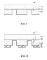
- the second portions 52 of the conductive structures 5 are formed such that they abut the second metal layer 74 (as shown in FIG. 9 , FIG. 10 , FIG. 11 , and FIG. 12 ), and thus, the upper surfaces 521 of the second portions 52 of the conductive structures 5 are substantially coplanar. As discussed above, the coplanarity of the upper surfaces 521 of the second portions 52 of the conductive structures 5 may be about ⁇ 15 ⁇ m, about ⁇ 7 ⁇ m, about ⁇ 3 ⁇ m, or less.
- a portion of the seed layer 48 may also be removed. Accordingly, a substrate structure 1 a is formed as shown in FIG. 2 . That is, the top portion 481 of the seed layer 48 is removed. Accordingly, the upper surface 511 a of the first portion 51 a is a surface of the conductive material 46 . Hence, the upper surface 61 of the first protective layer 6 may be higher than the upper surface 511 a of the first portion 51 a of the conductive structure 5 a.
- FIG. 17 , FIG. 18 , FIG. 19 , FIG. 20 , FIG. 21 , and FIG. 22 illustrate a method for manufacturing a substrate structure according to some embodiments of the present disclosure.
- the method is for manufacturing a substrate structure such as the substrate structure 1 b shown in FIG. 3 .
- the initial stages of the illustrated process are the same as the stages illustrated in FIG. 7 and FIG. 8 .
- FIG. 17 depicts a stage subsequent to that depicted in FIG. 8 .
- a first protective layer 6 is formed directly on and contacts the first photoresist 76 . That is, the stage for forming the auxiliary seed layer 49 as shown in FIG. 9 is omitted.
- the first protective layer 6 may include a solder resist material, for example, BCB or PI.
- the first protective layer 6 defines at least one second opening 60 , which communicates with the first opening 760 of the first photoresist 76 .
- the second opening 60 extends through the first protective layer 6 .
- a seed layer 48 is formed or disposed on the first protective layer 6 , and in the second opening 60 of the first protective layer 6 and the first opening 760 of the first photoresist 76 .
- the seed layer 48 may include, for example, titanium and/or copper, and may be formed or disposed by sputtering.
- a second photoresist 78 is formed on the first protective layer 6 and the seed layer 48 .
- the second photoresist 78 may include a dry film.
- the second photoresist 78 defines a plurality of circuit openings (e.g., circuit openings 780 a and 780 b ).
- the circuit openings e.g., the circuit openings 780 a and 780 b
- the circuit openings extend through the second photoresist 78 .
- At least one of the circuit openings (e.g., the circuit opening 780 a ) communicates with the second openings 60 of the first protective layer 6 .
- another one of the circuit openings does not communicate with the second openings 60 of the first protective layer 6 .
- the second photoresist 78 may include a photo-imageable material, and the circuit openings (e.g., the circuit openings 780 a and 780 b ) may be patterned by a lithography technique.
- a second portion 52 of a conductive structure 5 , a first portion 51 of the conductive structure 5 and a first circuit layer 4 are integrally formed in the first opening 760 of the first photoresist 76 , the second opening 60 of the first protective layer 6 and the circuit openings (e.g., the circuit openings 780 a and 780 b ) of the second photoresist 78 , respectively.
- a conductive material 46 is filled in the first opening 760 of the first photoresist 76 , the second opening 60 of the first protective layer 6 and the circuit openings (e.g., the circuit openings 780 a and 780 b ) of the second photoresist 78 by electroplating.
- the second portion 52 of the conductive structure 5 is formed in the first opening 760 of the first photoresist 76
- the first portion 51 of the conductive structure 5 is formed in the second opening 60 of the first protective layer 6
- the first protective layer 6 contacts at least a portion of the sidewall 514 of the first portion 51 .
- the second photoresist 78 is removed by, for example, stripping. Portions of the seed layer 48 which are not covered by the conductive material 46 are then removed by, for example, etching.
- the first circuit layer 4 is thus formed.
- the first circuit layer 4 includes a trace 42 and a bump pad 44 .
- the trace 42 is formed corresponding to the circuit opening 780 b which does not communicate with the second opening 60 of the first protective layer 6 .
- the bump pad 44 is formed corresponding to the circuit opening 780 a which communicates with the second opening 60 of the first protective layer 6 .
- the bump pad 44 has an upper surface 441 contacting the second surface 62 of the first protective layer 6 .
- the first portion 51 has an upper surface 511 and a sidewall 514 .
- the second portion 52 has an upper surface 521 and a sidewall 522 .
- the first portion includes the top portion 481 of the seed layer 48 disposed adjacent to the first surface 61 of the first protective layer 3 .
- the seed layer 48 surrounds the conductive material 46 .
- a dielectric layer 3 is formed or disposed on and covers the first protective layer 6 and the first circuit layer 4 .
- the dielectric layer 3 has a first surface 31 and a second surface 32 opposite to the first surface 31 .
- the first surface 31 of the dielectric layer 3 is disposed on the second surface 62 of the first protective layer 6 .
- the dielectric layer 3 defines an opening 30 that exposes a portion of the bump pad 44 of the first circuit layer 4 .
- a second circuit layer 8 is formed on the dielectric layer 3 and in the opening 30 of the dielectric layer 3 .
- the second circuit layer 8 includes a trace 82 and a conductive via 84 .
- the conductive via 84 is disposed in the opening 30 of the dielectric layer 3 and is connected to the bump pad 44 of the first circuit layer 4 .
- forming the trace 82 and the conductive via 84 of the second circuit layer 8 may include forming a seed layer 88 and a conductive material 86 on the seed layer 88 .
- a second protective layer 9 is formed on the second surface 32 of the dielectric layer 3 and covers at least a portion of the second circuit layer 8 .
- the second protective layer 9 has a first surface 91 and a second surface 92 opposite to the first surface 91 .
- the first surface 91 is disposed on the second surface 32 of the dielectric layer 3 .
- a portion of the conductive via 84 of the second circuit layer 8 is exposed from the second surface 92 of the second protective layer 9 .
- the carrier 70 , the first metal layer 72 and the second metal layer 74 are removed.
- the first photoresist 76 is removed by, for example, plasma removing or chemical etching techniques.
- the substrate structure 1 b as shown in FIG. 3 is thus formed.
- a portion of the first protective layer 6 may also be removed. That is, the first protective layer 6 is thinned from the first surface 61 of the first protective layer 6 . Accordingly, the first surface 61 of the first protective layer 6 may be slightly recessed from and lower than the upper surface 511 of the first portion 51 of the conductive structure 5 .
- FIG. 23 , FIG. 24 , FIG. 25 , FIG. 26 , and FIG. 27 illustrate a method for manufacturing a substrate structure according to some embodiments of the present disclosure.
- the method is for manufacturing a substrate structure such as the substrate structure 1 c shown in FIG. 4 .
- the initial stages of the illustrated process are the same as the stages illustrated in FIG. 7 , FIG. 8 , FIG. 9 , FIG. 10 and FIG. 11 .
- FIG. 23 depicts a stage subsequent to that depicted in FIG. 11 .
- a second portion 52 of a conductive structure 5 , a first portion 51 of the conductive structure 5 and a first circuit layer 4 are integrally formed in the first opening 760 of the first photoresist 76 , the second opening 60 of the first protective layer 6 and the circuit openings (e.g., the circuit openings 780 a and 780 b ) of the second photoresist 78 , respectively.
- a conductive material 46 is formed or disposed in the first opening 760 of the first photoresist 76 , the second opening 60 of the first protective layer 6 and the circuit openings (e.g., the circuit openings 780 a and 780 b ) of the second photoresist 78 by electroplating.
- the second portion 52 of the conductive structure 5 is formed in the first opening 760 of the first photoresist 76
- the first portion 51 of the conductive structure 5 is formed in the second opening 60 of the first protective layer 6 .
- the first opening 760 of the first photoresist 76 , the second opening 60 of the first protective layer 6 and the circuit opening (e.g., the circuit opening 780 a ) of the second photoresist 78 communicating with the second opening 60 may not be completely filled by the conductive material 46 .
- a first hole 440 may be formed in the first circuit layer 4 in the circuit openings 780 .
- a second hole 510 may be formed in the first portion 51 of the conductive structure 5 in the second opening 60 . The second hole 510 communicates with the first hole 440 of the first circuit layer 4 .
- a third hole 520 may be formed in the second portion 52 of the conductive structure 5 in the first opening 760 .
- the third hole 520 communicates with the second hole 510 of the first portion 51 of the conductive structure 5 .
- the first hole 440 has a minimum width W 3 .
- the second hole 510 has a minimum width W 4 .
- the minimum width W 3 of the first hole 440 of the first circuit layer 4 is greater than the minimum width W 4 of the second hole 510 of the first portion 51 of the conductive structure 5 .
- the third hole 520 has a minimum width W 5 .
- the minimum width W 4 of the second hole 510 of the first portion 51 of the conductive structure 5 is greater than the minimum width W 5 of the third hole 520 of the second portion 52 of the conductive structure 5 .
- forming the first circuit layer 4 in the circuit openings 780 includes forming a first hole 440 in the first circuit layer 4 in the circuit openings 780 .
- Forming the first portion 51 of the conductive structure 5 in the second opening 60 includes forming a second hole 510 in the first portion 51 of the conductive structure 5 in the second opening 60 , and the second hole 510 communicates with the first hole 440 of the first circuit layer 4 .
- Forming the second portion 52 of the conductive structure 5 in the first opening 760 includes forming a third hole 520 in the second portion 52 of the conductive structure 5 in the first opening 760 , and the third hole 520 communicates with the second hole 510 of the first portion 51 of the conductive structure 5 .
- the second photoresist 78 is removed by, for example, stripping. Portions of the seed layer 48 which are not covered by the conductive material 46 are then removed by, for example, etching. The first circuit layer 4 is thus formed.
- a dielectric layer 3 is formed or disposed on and covers the first protective layer 6 and the first circuit layer 4 .
- the dielectric layer 3 is filled in the first hole 440 of the circuit layer 4 in the circuit opening (e.g., the circuit opening 780 a ).
- the dielectric layer 3 is further filled in the second hole 510 of the first portion 51 of the conductive structure 5 in the second opening 60 .
- the dielectric layer 3 is further filled in the third hole 520 of the second portion 52 of the conductive structure 5 in the first opening 760 .
- the dielectric layer 3 defines an opening 30 to expose a portion of the first circuit layer 4 .
- a second circuit layer 8 is formed on the dielectric layer 3 and in the opening 30 of the dielectric layer 3 .
- the carrier 70 , the first metal layer 72 and the second metal layer 74 are removed.
- the first photoresist 76 is removed. Then, an etching process is conducted to remove the auxiliary seed layer 49 on the first protective layer 6 and on the conductive structure 5 , to expose the upper surface 521 and the sidewall 522 of the second portion 52 of the conductive structure 5 , the upper surface 511 of the first portion 51 of the conductive structure 5 , and the first surface 61 of the first protective layer 6 .
- the substrate structure 1 c as shown in FIG. 4 is thus formed.
- FIG. 28 , FIG. 29 , FIG. 30 , FIG. 31 , and FIG. 32 illustrate a method for manufacturing a substrate structure according to some embodiments of the present disclosure.
- the method is for manufacturing a substrate structure such as the substrate structure 1 d shown in FIG. 5 .
- the initial stages of the illustrated process are the same as the stage illustrated in FIG. 7 .
- FIG. 28 depicts a stage subsequent to that depicted in FIG. 7 .
- a first photoresist 76 is formed or disposed on the carrier 70 .
- the first photoresist 76 defines at least one first opening 760 .
- the first opening 760 extends through the first photoresist 76 .
- the first opening 760 is in a substantially trapezoidal shape.
- an auxiliary seed layer 49 is formed or disposed on the first photoresist 76 and in the first opening 760 of the first photoresist 76 .
- a first protective layer 6 is formed or disposed on the first photoresist 76 and the auxiliary seed layer 49 .
- the first protective layer 6 defines at least one second opening 60 , which communicates with the first opening 760 of the first photoresist 76 .
- the second opening 60 extends through the first protective layer 6 .
- a seed layer 48 is formed or disposed on the first protective layer 6 , and in the second opening 60 of the first protective layer 6 and the first opening 760 of the first photoresist 76 .
- the seed layer 48 is formed on the auxiliary seed layer 49 in the second opening 60 of the first protective layer 6 and in the first opening 760 of the first photoresist 76 .
- second photoresist 78 is formed on the first protective layer 6 and the seed layer 48 .
- the second photoresist 78 defines a plurality of circuit openings (e.g., circuit openings 780 a and 780 b ).
- the circuit openings (e.g., the circuit openings 780 a and 780 b ) extend through the second photoresist 78 .
- At least one of the circuit openings (e.g., the circuit opening 780 a ) communicates with the second openings 60 of the first protective layer 6 .
- the circuit opening (e.g., the circuit opening 780 a ) communicating with the second openings 60 of the first protective layer 6 is in a substantially trapezoidal shape.
- the first opening 760 of the first photoresist 76 , the second opening 60 of the first protective layer 6 and the circuit opening 780 of the second photoresist 78 which communicates with the second opening 60 are substantially in a tapered shape. In some embodiments, another one of the circuit openings (e.g., the circuit opening 780 b ) does not communicate with the second openings 60 of the first protective layer 6 .
- a second portion 52 of a conductive structure 5 , a first portion 51 of the conductive structure 5 and a first circuit layer 4 are integrally formed in the first opening 760 of the first photoresist 76 , the second opening 60 of the first protective layer 6 and the circuit openings (e.g., the circuit openings 780 a and 780 b ) of the second photoresist 78 , respectively. Then, the second photoresist 78 is removed. Portions of the seed layer 48 which are not covered by the conductive material 46 are then removed.
- stages subsequent to FIG. 32 of the illustrated process are similar to the stages illustrated in FIG. 13 , FIG. 14 , FIG. 15 , and FIG. 16 , thus forming the substrate structure 1 d as shown in FIG. 5 .
- the terms “approximately,” “substantially,” “substantial” and “about” are used to describe and account for small variations. When used in conjunction with an event or circumstance, the terms can refer to instances in which the event or circumstance occurs precisely as well as instances in which the event or circumstance occurs to a close approximation.
- the terms can refer to a range of variation less than or equal to ⁇ 10% of that numerical value, such as less than or equal to ⁇ 5%, less than or equal to ⁇ 4%, less than or equal to ⁇ 3%, less than or equal to ⁇ 2%, less than or equal to ⁇ 1%, less than or equal to ⁇ 0.5%, less than or equal to ⁇ 0.1%, or less than or equal to ⁇ 0.05%.
- two numerical values can be deemed to be “substantially” the same or equal if a difference between the values is less than or equal to ⁇ 10% of an average of the values, such as less than or equal to ⁇ 5%, less than or equal to ⁇ 4%, less than or equal to ⁇ 3%, less than or equal to ⁇ 2%, less than or equal to ⁇ 1%, less than or equal to ⁇ 0.5%, less than or equal to ⁇ 0.1%, or less than or equal to ⁇ 0.05%.
- two surfaces can be deemed to be coplanar or substantially coplanar if a displacement between the two surfaces is no greater than 15 ⁇ m, no greater than 7 ⁇ m, no greater than 5 ⁇ m, no greater than 3 ⁇ m, no greater than 2 ⁇ m, no greater than 1 ⁇ m, or no greater than 0.5 ⁇ m.
Landscapes
- Internal Circuitry In Semiconductor Integrated Circuit Devices (AREA)
- Engineering & Computer Science (AREA)
- Manufacturing & Machinery (AREA)
- Ceramic Engineering (AREA)
Abstract
Description
Claims (18)
Priority Applications (2)
| Application Number | Priority Date | Filing Date | Title |
|---|---|---|---|
| US15/665,289 US10354969B2 (en) | 2017-07-31 | 2017-07-31 | Substrate structure, semiconductor package including the same, and method for manufacturing the same |
| CN201711085518.XA CN109326574B (en) | 2017-07-31 | 2017-11-07 | Substrate structure, semiconductor package including the same, and method of manufacturing the same |
Applications Claiming Priority (1)
| Application Number | Priority Date | Filing Date | Title |
|---|---|---|---|
| US15/665,289 US10354969B2 (en) | 2017-07-31 | 2017-07-31 | Substrate structure, semiconductor package including the same, and method for manufacturing the same |
Publications (2)
| Publication Number | Publication Date |
|---|---|
| US20190035753A1 US20190035753A1 (en) | 2019-01-31 |
| US10354969B2 true US10354969B2 (en) | 2019-07-16 |
Family
ID=65039039
Family Applications (1)
| Application Number | Title | Priority Date | Filing Date |
|---|---|---|---|
| US15/665,289 Active US10354969B2 (en) | 2017-07-31 | 2017-07-31 | Substrate structure, semiconductor package including the same, and method for manufacturing the same |
Country Status (2)
| Country | Link |
|---|---|
| US (1) | US10354969B2 (en) |
| CN (1) | CN109326574B (en) |
Families Citing this family (6)
| Publication number | Priority date | Publication date | Assignee | Title |
|---|---|---|---|---|
| CN109729639B (en) * | 2018-12-24 | 2020-11-20 | 奥特斯科技(重庆)有限公司 | Component carrier including pillars on a coreless substrate |
| JP7240909B2 (en) * | 2019-03-13 | 2023-03-16 | 新光電気工業株式会社 | Wiring board and its manufacturing method |
| US11139232B2 (en) * | 2020-03-06 | 2021-10-05 | Advanced Semiconductor Engineering, Inc. | Wiring structure and method for manufacturing the same |
| US12354935B2 (en) * | 2020-08-25 | 2025-07-08 | Qualcomm Incorporated | Integrated circuit (IC) package substrate with embedded trace substrate (ETS) layer on a substrate, and related fabrication methods |
| US12100645B2 (en) | 2021-09-23 | 2024-09-24 | Qualcomm Incorporated | Integrated circuit (IC) package employing added metal for embedded metal traces in ETS-based substrate for reduced signal path impedance, and related fabrication methods |
| US12362269B2 (en) * | 2021-10-18 | 2025-07-15 | Qualcomm Incorporated | Integrated circuit (IC) packages employing supplemental metal layer coupled to embedded metal traces in a die-side embedded trace substrate (ETS) layer, and related fabrication methods |
Citations (2)
| Publication number | Priority date | Publication date | Assignee | Title |
|---|---|---|---|---|
| TWM433634U (en) | 2012-03-23 | 2012-07-11 | Unimicron Technology Corp | Semiconductor substrate |
| US9282640B2 (en) | 2007-08-15 | 2016-03-08 | Tessera, Inc. | Interconnection element with posts formed by plating |
Family Cites Families (3)
| Publication number | Priority date | Publication date | Assignee | Title |
|---|---|---|---|---|
| US7405149B1 (en) * | 1998-12-21 | 2008-07-29 | Megica Corporation | Post passivation method for semiconductor chip or wafer |
| KR100538633B1 (en) * | 2003-11-13 | 2005-12-22 | 매그나칩 반도체 유한회사 | Method of forming a metal wiring in a semiconductor device |
| US7956463B2 (en) * | 2009-09-16 | 2011-06-07 | International Business Machines Corporation | Large grain size conductive structure for narrow interconnect openings |
-
2017
- 2017-07-31 US US15/665,289 patent/US10354969B2/en active Active
- 2017-11-07 CN CN201711085518.XA patent/CN109326574B/en active Active
Patent Citations (3)
| Publication number | Priority date | Publication date | Assignee | Title |
|---|---|---|---|---|
| US9282640B2 (en) | 2007-08-15 | 2016-03-08 | Tessera, Inc. | Interconnection element with posts formed by plating |
| TWM433634U (en) | 2012-03-23 | 2012-07-11 | Unimicron Technology Corp | Semiconductor substrate |
| US20130249083A1 (en) | 2012-03-23 | 2013-09-26 | Unimicron Technology Corporation | Packaging substrate |
Also Published As
| Publication number | Publication date |
|---|---|
| US20190035753A1 (en) | 2019-01-31 |
| CN109326574B (en) | 2020-09-11 |
| CN109326574A (en) | 2019-02-12 |
Similar Documents
| Publication | Publication Date | Title |
|---|---|---|
| US10354969B2 (en) | Substrate structure, semiconductor package including the same, and method for manufacturing the same | |
| US11913121B2 (en) | Fabrication method of substrate having electrical interconnection structures | |
| CN112233989B (en) | Stacked package structure and forming method thereof | |
| US20200258826A1 (en) | Semiconductor package and semiconductor manufacturing process | |
| US20190206824A1 (en) | Semiconductor package structure and method for manufacturing the same | |
| US11705341B2 (en) | Method of fabricating a semiconductor package having redistribution patterns including seed patterns and seed layers | |
| CN107393894A (en) | Integrated fan-out package | |
| US11538798B2 (en) | Semiconductor package with multiple redistribution substrates | |
| US20190043819A1 (en) | Electronic package having redistribution structure | |
| CN110473843A (en) | Semiconductor package and manufacturing method thereof | |
| KR102826729B1 (en) | Semiconductor device and manufacturing method thereof | |
| US9984898B2 (en) | Substrate, semiconductor package including the same, and method for manufacturing the same | |
| US20250279375A1 (en) | Electronic package and manufacturing method thereof | |
| US20200273722A1 (en) | Semiconductor package structure and method for manufacturing the same | |
| US9117697B2 (en) | Semiconductor substrate and method for making the same | |
| US10629558B2 (en) | Electronic device | |
| US12183593B2 (en) | Manufacturing method for manufacturing a package structure | |
| US20200303333A1 (en) | Electronic package and manufacturing method thereof | |
| US11398419B2 (en) | Wiring structure and method for manufacturing the same | |
| US20220199509A1 (en) | Wiring structure and method for manufacturing the same | |
| US11973039B2 (en) | Semiconductor device package and method of manufacturing the same | |
| US11217520B2 (en) | Wiring structure, assembly structure and method for manufacturing the same | |
| KR20220034596A (en) | Semiconductor package | |
| US11610834B2 (en) | Leadframe including conductive pillar over land of conductive layer | |
| US20250183140A1 (en) | Integrated circuit packages and methods of forming the same |
Legal Events
| Date | Code | Title | Description |
|---|---|---|---|
| AS | Assignment |
Owner name: ADVANCED SEMICONDUCTOR ENGINEERING, INC., TAIWAN Free format text: ASSIGNMENT OF ASSIGNORS INTEREST;ASSIGNORS:SHIH, YU-LIN;LEE, CHIH-CHENG;REEL/FRAME:043404/0572 Effective date: 20170726 |
|
| STPP | Information on status: patent application and granting procedure in general |
Free format text: FINAL REJECTION MAILED |
|
| STPP | Information on status: patent application and granting procedure in general |
Free format text: RESPONSE AFTER FINAL ACTION FORWARDED TO EXAMINER |
|
| STPP | Information on status: patent application and granting procedure in general |
Free format text: NOTICE OF ALLOWANCE MAILED -- APPLICATION RECEIVED IN OFFICE OF PUBLICATIONS |
|
| STPP | Information on status: patent application and granting procedure in general |
Free format text: PUBLICATIONS -- ISSUE FEE PAYMENT VERIFIED |
|
| STPP | Information on status: patent application and granting procedure in general |
Free format text: AWAITING TC RESP, ISSUE FEE PAYMENT VERIFIED |
|
| STPP | Information on status: patent application and granting procedure in general |
Free format text: PUBLICATIONS -- ISSUE FEE PAYMENT VERIFIED |
|
| STCF | Information on status: patent grant |
Free format text: PATENTED CASE |
|
| MAFP | Maintenance fee payment |
Free format text: PAYMENT OF MAINTENANCE FEE, 4TH YEAR, LARGE ENTITY (ORIGINAL EVENT CODE: M1551); ENTITY STATUS OF PATENT OWNER: LARGE ENTITY Year of fee payment: 4 |