US10340918B2 - Level shifter - Google Patents
Level shifter Download PDFInfo
- Publication number
- US10340918B2 US10340918B2 US15/968,829 US201815968829A US10340918B2 US 10340918 B2 US10340918 B2 US 10340918B2 US 201815968829 A US201815968829 A US 201815968829A US 10340918 B2 US10340918 B2 US 10340918B2
- Authority
- US
- United States
- Prior art keywords
- switch element
- voltage
- path terminal
- terminal
- node
- Prior art date
- Legal status (The legal status is an assumption and is not a legal conclusion. Google has not performed a legal analysis and makes no representation as to the accuracy of the status listed.)
- Active
Links
Images


Classifications
-
- H—ELECTRICITY
- H03—ELECTRONIC CIRCUITRY
- H03K—PULSE TECHNIQUE
- H03K19/00—Logic circuits, i.e. having at least two inputs acting on one output; Inverting circuits
- H03K19/0175—Coupling arrangements; Interface arrangements
- H03K19/017509—Interface arrangements
-
- H—ELECTRICITY
- H03—ELECTRONIC CIRCUITRY
- H03K—PULSE TECHNIQUE
- H03K19/00—Logic circuits, i.e. having at least two inputs acting on one output; Inverting circuits
- H03K19/0175—Coupling arrangements; Interface arrangements
- H03K19/0185—Coupling arrangements; Interface arrangements using field effect transistors only
- H03K19/018507—Interface arrangements
- H03K19/018521—Interface arrangements of complementary type, e.g. CMOS
-
- H—ELECTRICITY
- H03—ELECTRONIC CIRCUITRY
- H03K—PULSE TECHNIQUE
- H03K19/00—Logic circuits, i.e. having at least two inputs acting on one output; Inverting circuits
- H03K19/20—Logic circuits, i.e. having at least two inputs acting on one output; Inverting circuits characterised by logic function, e.g. AND, OR, NOR, NOT circuits
Definitions
- the invention relates in general to a level shifter, and more particularly to a level shifter with a high response speed.
- a level shifter is used to convert an input signal having a certain voltage amplitude to an output signal having a different voltage amplitude, and is extensively applied in different types of integrated circuits having different operating voltages.
- a current level shifter and specifically a charge pump level shifter, has a low operating speed and is not suitable for operating in a high frequency. More particularly, a conventional level shifter usually adopts an input/output (IO) device, of which a high threshold voltage and a low input voltage amplitude severely affect the response speed of the IO device, resulting in an overall slow operating speed of the level shifter.
- IO input/output
- the present invention provides a level shifter including a bias voltage providing circuit, a level shifting circuit and an output switching circuit.
- the bias voltage providing circuit includes: a bias voltage providing unit, disposed between a first operating voltage and a ground voltage, providing a first bias voltage; and a second bias voltage providing unit, disposed between the first operating voltage and the ground voltage, providing a second bias voltage.
- the level shifting circuit includes: a high level shifting unit, receiving a first control signal and connected to the first operating voltage, determining whether to conduct the high level shifting circuit according to the first control signal to accordingly determine whether to output the first operating voltage; and a low level shifting unit, receiving the first control signal and connected to the second operating voltage, determining whether to conduct the low level shifting unit according to the first control signal to accordingly determine whether to output the second operating voltage.
- the output switching circuit includes a first switch element and a second switch element.
- the first switch element includes a control terminal, a first path terminal and a second path terminal, wherein the control terminal receives a first control voltage, and the first path terminal receives an output of the level shifting circuit; wherein, when the level shifting circuit outputs the first operating voltage, the first switch element is conducted to enable the output switching circuit to output the first operating voltage, and when the level shifting circuit outputs the second operating voltage, the first switch element is cut off.
- the second switch element includes a control terminal, a first path terminal and a second path terminal, wherein the first control terminal receives a second control voltage, and the first path terminal receives the second control signal; wherein, the second control signal is configured to match the operation of the first switch element, such that the second switch element is cut off when the first switch element is conducted, and the first switch element is cut off when the second switch element is conduct to cause the output switching circuit to output the ground voltage; the first switch element is a first-type switch element, the second switch element is a second-type switch element, and the type of the first-type switch element is different from the type of the second-type switch element.
- the high level shifting circuit When the high level shifting unit is in a cut-off state, the high level shifting circuit further receives the first bias voltage such that the high level shifting circuit is in a partially cut-off state. When the low level shifting unit is in a cut-off state, the low level shifting circuit further receives the second bias voltage such that the low level shifting circuit is in a partially cut-off state.
- the level shifter of the present invention allows the high level shifting unit and the low level shifting unit to be in a partially cut-off state to accordingly increase a response speed thereof. Further, the core devices and the first-type IO devices also significantly increase the response speed, thus enhancing the overall operation speed of the device and allowing the device to operate in high frequencies.
- FIG. 1 is a block diagram of a level shifter according to an embodiment of the present invention
- FIG. 2 is a brief schematic diagram of the level shifter according to an embodiment of the present invention.
- FIG. 3 is a circuit schematic diagram of the level shifter in FIG. 1 and FIG. 2 according to an embodiment of the present invention.
- the present invention provides a level shifter. Details of the present invention are given in the embodiments with the accompanying drawings below.
- FIG. 1 shows a block diagram of a level shifter according to an embodiment of the present invention.
- the level shifter 100 includes a bias voltage providing circuit 110 , a level shifting circuit 120 and an output switching circuit 130 .
- the bias voltage providing circuit 110 includes a first bias voltage providing unit 111 and a second bias voltage providing unit 112 .
- the first bias voltage providing unit 111 is disposed between a first operating voltage vddio and a ground voltage, and provides a first bias voltage.
- the second bias voltage providing unit 112 is also disposed between the first operating voltage vddio and the ground voltage, and provides a second bias voltage.
- the first operating voltage vddio may be set to 3.3V.
- the level shifting circuit 120 includes a high level shifting unit 121 and a low level shifting unit 122 .
- the high level shifting unit 121 is connected to the first operating voltage vddio, receives a first control signal UPB, and determines whether to conduct the high level shifting unit 122 according to the first control signal UPB to further determine whether to output the first operating voltage vddio.
- the low level shifting unit 122 is connected to a second operating voltage dvdd, receives the first control signal UPB, and determines whether to conduct the low level shifting unit 122 according to the first control signal UPB to further determine whether to output the second operating voltage dvdd.
- the first control signal UPB is a pulse width modulation (PWM) signal formed by the ground voltage and the second operating voltage dvdd.
- PWM pulse width modulation
- the second operating voltage dvdd may be set to 1.1V
- the output switching circuit 130 includes switch elements T 1 and T 2 .
- each of the switch elements described below includes a control terminal, a first path terminal and a second path terminal, and may be implemented by a transistor.
- the control terminal of the switch element refers to the gate of a transistor
- the first path terminal of the switch element refers to the source of a transistor
- the second path terminal of the switch element refers to the drain of a transistor.
- the control terminal of the switch element T 1 receives a first control voltage Vbp, and the first path terminal receives an output of the level shifting circuit 120 .
- the switch element T 1 is conducted so as cause the output switching circuit 130 to output the first operating voltage vddio.
- the switch element T 1 is cut-off.
- the control terminal of the switch element T 2 receives a second control voltage Vbn, and the first path terminal receives a second control signal DN.
- the second control signal DN is similarly a PWM signal formed by the ground voltage and the second operating voltage dvdd, and is designed to match the operation of the switch element T 1 , such that the switch element T 2 is cut off when the switch element T 1 is conducted, and the switch element T 1 is cut off when the switch element T 2 is conducted so as to enable the output switching circuit 300 to output the ground voltage.
- the second control signal DN may be designed as, the switch element T 2 is cut off when the second control signal DN is the ground voltage, and the switch element T 2 is conducted when the second control signal DN is the second operating voltage dvdd, so as to enable the output switching circuit 130 to output the ground voltage.
- the switch element T 1 is a first-type switch element
- the switch element T 2 is a second-type switch element
- the type of the first-type switch element is different from the type of the second-type switch element.
- the switch element T 1 is a PMOS transistor
- the switch element T 2 is an NMOS transistor.
- the high level shifting unit 121 when the high level shifting unit 121 is in a cut-off state, it further receives a first bias voltage provided by the first bias voltage providing unit 111 , such that the high level shifting unit 121 is in a partially cut-off state, thus increasing the response speed of the high level shifting unit 121 .
- the low level shifting unit 122 when the low level shifting unit 122 is in a cut-off state, it further receives a second bias voltage provided by the first bias voltage providing unit 112 , such that the low level shifting unit 122 is in a partially cut-off state, thus increasing the response speed of the low level shifting unit 122 .
- the bias voltage providing circuit 110 before the level shifting circuit 120 is further designed to provide a bias voltage to the level shifting circuit 120 , such that some components originally in a cut-off state may become in a partially cut-off state when the level shifting circuit 120 switches between the first operating voltage vddio and the second operating voltage dvdd.
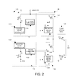
- FIG. 2 shows a brief schematic diagram of the level shifter in FIG. 1 according to an embodiment of the present invention.
- the first bias voltage providing unit 111 in this embodiment includes a switch element T 3 , a first bias current providing circuit 1111 and a first voltage buffer circuit 1112 .
- the first path terminal of the switch element T 3 is connected to the first operating voltage vddio, and the control terminal and the second path terminal thereof are connected together at a connecting position defined as a first node A.
- the first bias current providing circuit 1111 is connected to the first node A, and is connected to the switch element T 3 via the first node A to further provide the switch element T 3 with a bias current, so as to enable the switch element T 3 to generate the first bias voltage at the first node A.
- the first voltage buffer circuit 1112 is also connected to the node A to buffer the first bias voltage outputted.
- the high level shifting unit 121 includes a switch element T 4 and a first source follower circuit 1210 .
- the first path terminal of the switch element T 4 is also connected to the first operating voltage vddio, and the second path terminal serves as an output end of the high level shifting unit 121 and is connected to the low level shifting unit 122 .
- the first source follower circuit 1210 is connected to the control terminal of the switch element T 4 at a connecting position defined as a second node B.
- the first source follower circuit 1210 is connected to the first bias voltage providing unit 111 via the second node B in a way that the voltage at the second node B changes with a change in the first bias voltage, such that the switch element T 4 is in a partially cut-off state when the high level shifting unit 121 is in a cut-off state.
- the first bias current providing circuit 1111 in the first bias voltage providing unit 111 provides a bias current to the switch element T 3 to enable the switch element T 3 to generate the first bias voltage at the first node A; with the first voltage buffer circuit 1112 and the first source follower circuit 1210 in the high level shifting unit 121 , the voltage at the second node B changes with the change in the first bias voltage at the first node A.
- the switch element T 4 can be in a partially cut-off state.
- the second bias voltage providing unit 112 includes switch element T 5 , a second bias current providing circuit 1121 and a second voltage buffer circuit 1122 .
- the first path terminal of the switch element T 5 is connected to the second operating voltage dvdd, and the control terminal and the second path terminal thereof are connected together at a connecting position defined as a third node C.
- the second bias current providing circuit 1121 is connected to the third node C, and is connected to the switch element T 5 via the node C to provide the switch element T 5 with a bias current, so as to enable the switch element T 5 to generate a second bias voltage at the third node C.
- the second voltage buffer circuit 1122 is connected to the third node C to buffer the second bias voltage outputted.
- the low shifting unit 1220 includes a switch element T 6 and a second source follower circuit 1220 .
- the first path terminal of the switch element T 6 is connected to the second operating voltage dvdd, and the second path terminal thereof serves as an output end of the low level shifting unit 122 and is connected to the high level shifting unit 121 .
- the second source follower circuit 1220 is connected to the control terminal of the switch element T 6 at a connecting position defined as a fourth node D, and is connected to the second bias voltage providing unit 112 via the fourth node D in a way that the voltage at the fourth node D changes with a change in the second bias voltage, such that the switch element T 6 is in a partially cut-off state when the low level shifting unit 122 is in a cut-off state.
- FIG. 3 shows a circuit schematic diagram of the level shifter in FIGS. 1 and 2 according to an embodiment of the present invention. The present invention is further described with reference to FIGS. 1 to 3 .
- the first bias current providing circuit 1111 in the first bias voltage providing unit 111 includes switch elements T 7 and T 8 .
- the first voltage buffer circuit 1112 includes a first operational amplifier 11121 and switch elements T 9 and T 10 .
- the first path terminal of the switch element T 7 is connected to the ground voltage, and the control terminal and the second path terminal are connected to a first voltage source V 1 , i.e., a voltage source provided from an external terminal.
- the control terminal of the switch element T 8 is connected to the first voltage source V 1 , and the first path terminal is connected to the ground voltage.
- the first operational amplifier 11211 includes a positive input end, a negative input end and an output end, wherein the negative input end is connected to the first node A.
- the control end of the switch element T 9 is connected to the second operating voltage dvdd, and the second path terminal is connected to the ground voltage.
- the control terminal of the switch element T 10 is connected to the output end of the first operational amplifier 11211 , the first path terminal is connected to the first operating voltage vddio, and the second path terminal is connected to the first path terminal of the switch element T 9 at a connecting position defined as a fifth node E.
- the positive input end of the first operational amplifier 11211 is further connected to the fifth node E.
- the first source follower circuit 1210 in the high level shifting unit 121 includes switch elements T 11 and T 12 .
- the control terminal of the switch element T 11 is connected to the output end of the operational amplifier 11211 , and the first path terminal is connected to the first operating voltage vddio.
- the control terminal of the switch element T 12 receives the first control signal UPB, the second path terminal thereof is connected to the ground voltage, and the first path terminal thereof is connected to the second path terminal of the switch element T 11 .
- a connecting position between the second path terminal of the switch element T 11 and the first terminal path of the switch element T 12 is the second node B, which is further connected to the control terminal of the switch element T 4 .
- the second bias current providing circuit 1121 in the second bias voltage providing unit 112 includes switch elements T 13 and T 14
- the second voltage buffer circuit 1122 includes a second operational amplifier 11221 and switch elements T 15 and T 16 .
- the first path terminal of the switch element T 13 is connected to the first operating voltage vddio, and both of the control terminal and the second path terminal thereof are connected to a second voltage source V 2 , i.e., a voltage source provided from an external terminal.
- the control terminal of the switch element T 14 is connected to the second voltage source V 2 , and the first path terminal is connected to the first operating voltage vddio.
- the second operational amplifier 11221 includes a positive end, a negative end and an output end, wherein the negative input end is connected to the third node C.
- the control terminal of the switch element T 15 is connected to the output end of the second operational amplifier 11221 , and the first path terminal is connected to the first operating voltage vddio.
- the control terminal and the second path terminal of the switch element T 16 are connected to the ground voltage, and the first path terminal is connected to the second path terminal of the switch element T 15 at a connecting position defined as a sixth node F. Further, the positive input end of the second operational amplifier 11221 is connected to the sixth node F.
- the second source follower circuit 1220 in the low level shifting unit 122 includes switch elements T 17 and T 18 .
- the control terminal of the switch element T 17 is connected to the output end of the second operational amplifier 11221 , and the first path terminal thereof is connected to the first operating voltage vddio.
- the control terminal of the switch element T 18 receives the first control signal UPB, the second path terminal is connected to the ground voltage, and the first path terminal is connected to the second path terminal of the switch element T 17 .
- a connecting position between the second path terminal of the switch element T 17 and the first path terminal of the switch element T 18 is the fourth node D, which is further connected to the control terminal of the switch element T 6 .
- the switch elements T 3 , T 3 , T 9 , T 10 , T 11 , T 12 , T 13 , T 14 , T 15 , T 16 , T 17 and T 18 are first-type switch elements, i.e., PMOS transistors, and the switch elements T 5 , T 6 , T 7 and T 8 are second-type switch elements, i.e., NMOS transistors.
- the high level shifting unit 121 may further include a capacitor C 1 , which is disposed between the control terminal of the switch T 12 and the second node B.
- the low level shifting unit 122 may further include a capacitor C 2 , which is disposed between the control terminal of the switch element T 18 and the fourth node D.
- the output switching circuit 130 may further include a first buffer unit 131 and a second buffer unit 132 .
- the first buffer unit 131 is disposed between the output end of the level shifting circuit 120 and the first path terminal of the switch element T 1 .
- the second buffer unit 132 is disposed between the second control signal DN and the first path terminal of the switch element T 2 .
- Each of the first buffer unit 131 and the second buffer unit 132 may be formed by multiple inverters.
- the first buffer unit 131 includes a first inverter 1311 and a second inverter 1312 .
- the first inverter 1311 and the second inverter 1312 are both disposed between the first operating voltage vddio and the second operating voltage dvdd, and each includes an input end and an output end.
- first inverter 1311 and the second inverter 1312 are connected in series, the input end of the first inverter 1311 is connected to the output end of the level shifting circuit 120 , and the output end of the second inverter 1312 is connected to the first path terminal of the switch element T 1 , so as to transmit the output of the level shifting circuit 120 to the first path terminal of the first switch element T 1 .
- the second buffer unit 132 includes a third inverter 1321 , a fourth inverter 1322 and a fifth inverter 1323 .
- the third inverter 1321 , the fourth inverter 1322 and the fifth inverter 1323 are connected in series and are disposed between the second operating voltage dvdd and the ground voltage, and each includes an input end and an output end.
- the input end of the third inverter 1321 receives the second control signal DN
- the input end of the fourth inverter 1322 is connected to the output end of the third inverter 1321
- the input end of the fifth inverter 1323 is connected to the output end of the fourth inverter 1322
- the output end of the fifth inverter 1323 is connected to the first path terminal of the switch element T 2 , so as to transmit an inverted signal of the second control signal DN to the first path terminal of the switch element T 2 .
- the third inverter 1321 , the fourth inverter 1322 and the fifth inverter 1323 in the second buffer unit 132 are implemented by core devices; the switch elements T 3 , T 4 , T 5 and T 6 and the first inverters 1311 and the second inverters 1312 in the first buffer unit 131 are implemented by first-type IO devices; and the remaining devices, such as the switch elements T 1 , T 2 and T 7 to T 18 , the first operational amplifier 11121 and the second operational amplifier 11221 are all implemented by second-type IO devices.
- the driving voltage of the first-type IO devices is lower than the driving voltage of the second-type IO devices.
- the switch element T 3 in the first bias voltage providing unit 111 in the bias voltage providing circuit 110 , the switch element T 3 is a first-type IO device, and the other components are second-type IO devices.
- the switch element T 5 in the second bias voltage providing unit 112 , the switch element T 5 is a first-type IO device, and the other components are all second-type IO devices.
- the switch element T 4 is a first-type IO device, and the switch elements T 11 and T 12 are second-type IO devices.
- the switch element T 6 is a first-type IO device
- the switch elements T 17 and T 18 are second-type IO devices.
- the switch elements T 1 and T 2 in the output switching circuit 130 are implemented by second-type IOD devices.
- the first inverter 1311 and the second inverter 1312 in the first buffer unit 131 are first-type IO devices
- the third inverter 1321 , the fourth inverter 1322 and the fifth inverter 1323 in the second buffer unit 132 are core devices.
- a core device usually has a higher speed and a more robust driving capability, but can withstand a lower voltage difference.
- An IO device has a lower speed and a weaker driving capability, but can withstand a higher voltage difference. Therefore, in the present invention, the core devices require a lower the driving voltage but can only operate in an environment having a lower voltage difference; the IO devices require a higher driving voltage but can operate in an environment having a larger voltage difference.
- the first-type IO devices may be 2.5V IO devices
- the second-type IO devices may be 3.3V IO devices. That is to say, the first-type IO devices can only withstand a voltage difference of 2.5V but require a lower driving voltage, whereas the second-type IO devices can withstand a voltage difference of 3.3V but require a higher driving voltage. Operation principles of the above level shifter are further given below.
- the first voltage source V 1 is a high voltage source
- the second voltage source V 2 is a low voltage source, e.g., a ground voltage.
- the switch element T 8 Because the switch element T 8 is conducted, the ground voltage discharges the first node A via the conducted switch element T 8 , i.e., the conducted switch element T 8 transmits the ground voltage to the first node A. At this point, the voltage at the first node A is a low voltage, i.e., logic “0”.
- the switch element T 3 is a PMOS transistor, and has the first path terminal thereof connected to the first operating voltage vddio (i.e., a high voltage). Thus, the switch element T 3 is conducted, and the first operating voltage vddio charges the switch element T 3 to pull up the voltage at the first node A.
- the switch element T 8 is maintained in a conducted state, and so the ground voltage discharges the first node A via the conducted switch element T 8 , and the first operating voltage vddio charges the first node A via the conducted switch element T 3 , both achieving a balanced state. That is to say, during operation, the first node A has a certain level of voltage, which is higher than the ground voltage and lower than the first operating voltage vddio.
- the switch elements T 13 and T 14 in the second bias current providing circuit 1121 are both conducted, and the current IB flows out via the conducted switch element T 13 .
- the switch element T 14 Because the switch element T 14 is conducted, the first operating voltage vddio charges the third node C to pull up the voltage at the third node C.
- the switch element T 5 When the voltage at the third node C is pulled up to a certain level, the switch element T 5 is conducted, and the second operating voltage dvdd discharges the third node C via the conducted switch element T 5 , both reaching a balanced state.
- the third node C also has a certain level of voltage, which is higher than the second operating voltage dvdd (1.1V) and lower than the first operating voltage vddio (3.3V).
- the control terminal of the switch element T 9 is connected to the second operating voltage dvdd (1.1V).
- the switch element T 9 is in a cut-off state, and cannot be conducted easily.
- the fifth node E in an initial stage is in a virtual state, i.e., level “0”. Because the positive input end of the first operational amplifier 11121 is connected to the fifth node E, the voltage at the positive input end of the first operational amplifier 11121 in the initial stage is smaller than the voltage at the negative input end of the operational amplifier 11121 , i.e., logic “0”. In the above condition, the switch element T 10 is conducted, and the first operating voltage vddio charges the fifth node E via the conducted switch element T 10 to pull up the voltage at the fifth node E.
- the voltage at the positive input end of the first operational amplifier 11121 is also pulled up, i.e., a voltage difference between the positive input end and the negative input end is reduced, and thus the voltage outputted from the output end of the first operational amplifier 11121 increases.
- the voltage difference between the control terminal and the first path terminal of the switch element T 10 is reduced, and the switch element T 10 is gradually cut off.
- the voltages at the fifth node E, the positive end and the negative end of the first operational amplifier 111211 should become consistent.
- a circuit formed by the switch elements T 1 to T 12 in the first source follower circuit 1210 is the same as the circuit formed by the switch elements T 9 and T 10 .
- the second node B is similar to the fifth node E, and also has a certain level of voltage, that is, the voltage at the second node B is expected to be equal to the voltage at the negative input end of the first operational amplifier 11121 .
- the switch element T 4 in the high level shifting unit 121 is in a cut-off state.
- the sixth node F in the initial stage is in a virtual state, i.e., level “0”. Because the positive input end of the second operational amplifier 11221 is connected to the sixth node F, the voltage at the positive input end of the second operational amplifier 11221 in the initial stage is lower than the voltage at the negative input end of the second operational amplifier 11221 . Thus, the second operational amplifier 11221 outputs a low voltage. At this point, the switch element T 15 is conducted, and the first operating voltage vddio charges the sixth node F via the conducted switch element T 15 to pull up the voltage at the sixth node F.
- the voltage at the positive input end of the second operational amplifier 11221 is also pulled up, that is, a voltage difference between the positive input end and the negative input end of the second operational amplifier 11221 is reduced.
- control terminal of the switch element T 16 is connected to the ground voltage.
- the switch element T 16 is conducted, and the ground voltage discharges the sixth node F via the conducted switch element T 16 , i.e., pulling down the voltage at the sixth node F.
- the first operating voltage vddio (3.3V) charges the sixth node F via the switch element T 15
- the ground voltage discharges the sixth node F via the switch element T 16
- the second operational amplifier 11221 adjusts a conduction level or cut-off level of the switch element T 15 according to the voltage values at the negative input end and the positive input end of the second operational amplifier 11221 to reach a certain level of balance.
- the switch element T 17 is similar to the switch element T 15 and is controlled by the voltage outputted from the output end of the second operational amplifier 11221 . That is to say, when the switch element T 15 is conducted and the first operating voltage vddio charges the sixth node F, the switch element T 17 is also conducted and the first operating voltage vddio similarly charges the fourth node D.
- a circuit formed by the switch elements T 17 and T 18 does not include a discharging path (because the switch element T 18 is connected to the first control signal UPB at the second operating voltage dvdd, and is in a cut-off state), that is, the fourth node D is charged by only the first operating voltage vddio via the switch element T 17 .
- the voltage at the third node C is higher than the second operating voltage dvdd (1.1V) and is lower than the first operating voltage vddio (3.3V), and the voltage at the sixth voltage F is approximately consistent with the voltage at the third node C, and is definitely higher than the second operating voltage dvdd (1.1V).
- the voltage at the fourth node D is definitely higher than the voltage at the sixth node F.
- the switch element T 6 in the low level shifting unit 122 despite that the first path terminal thereof is connected to the second operating voltage dvdd, the control terminal thereof is however connected to the fourth node D. During this process, a large voltage value is gathered on the fourth node D, and so the switch element T 6 is conducted.
- the switch element T 6 is a first-type IO device (2.5V IO device), and can be conducted without a particularly high voltage.
- the switch element T 4 is cut off, i.e., that high level shifting circuit 121 in the left shifter 120 is cut off, and the switch element T 6 is conducted, i.e., the low level shifting circuit 122 in the level shifter 120 is conducted. Accordingly, the level shifter 120 outputs the second operating voltage dvdd via the conducted switch element T 6 .
- the circuit formed by the switch elements T 4 and T 6 is similar to the circuit formed by the switch elements T 3 and T 8 .
- the switch element T 8 is in a conducted state under the effect of the first voltage source V 1 , the ground voltage discharges the first node A via the conducted switch element T 8 , and the voltage at the first node A is pulled down. If the voltage at the first node A is pulled down to a certain level, the switch element T 3 is conducted, and the first operating voltage vddio charges the first node A via the conducted switch element T 3 to pull up the voltage at the first node A. Thus, the voltage at the first node A rises, and the switch element T 3 is cut off.
- the first bias current providing circuit 1111 provides the switch element T 3 with a bias current in a way that a specific first bias voltage is generated at the first node A. Further, because the first node A is also connected to the control terminal of the switch element T 3 , the first bias voltage at the first node A causes the switch element T 3 to be in a partially cut off state, and once the first bias voltage at the first node A is reduced to a certain level, the first operating voltage vddio quickly replenishes the voltage at the first node A. In other words, during this process, leakage current flows through the switch element T 3 to replenish the voltage at the first node A, and the switch element T 3 is extremely sensitive.
- the voltage at the second node B charges with a change in the first bias voltage at the first node A (i.e., the voltage at the negative input end of the first operational amplifier 11121 ).
- the switch element T 4 is also in a partially cut off state, and leakage current flows through the switch element T 4 .
- the switch element T 4 and the switch element T 3 are both first-type IO devices (2.5V IO devices), and therefore do not require a high driving voltage.
- the switch element T 12 in the first source follower circuit 1210 is conducted.
- the ground voltage discharges the second node B via the conducted switch element T 12 to pull down the voltage at the second node B.
- the switch element T 4 is conducted. More particularly, because the switch element T 4 is previously in a partially cut-off state, it can switch to a conducted state extremely fast. That is to say, the response speed of the high level shifting unit 121 is higher.
- the capacitor C 1 is further provided between the control terminal of the switch element T 2 and the second node B.
- the first control signal UPB received by the control terminal of the switch element T 12 is switched from the second operating voltage dvdd to the ground voltage, i.e., the voltage at the control terminal of the switch element T 12 jumps from the second operating voltage dvdd to the ground voltage, due to a coupling effect (bootstrap effect) of the capacitor C 1 , a voltage jump will also occur in the voltage at the second node B, which then changes towards the ground voltage. That is to say, the capacitor C 1 provided further promotes the discharging on the voltage at the second node B to pull down the voltage at the second node B.
- the capacitor C 1 provided can further enhance the response speed of the high level shifting unit 121 , enabling the high level shifting unit 121 to be free from limitations of the switching speed of the switch element T 12 .
- the switch element T 18 in the low level shifting unit 122 is conducted.
- the ground voltage discharges via the switch element T 18 to pull down the voltage at the fourth node D.
- the switch element T 6 is cut off.
- the capacitor C 2 between the control terminal of the switch element T 18 and the fourth node D further enhances the response speed of the low level shifting unit 122 , enabling the low level shifting unit 122 to be free from limitations of the switching speed of the switch element T 18 .
- the switch element T 4 is conducted, which is equivalently conducting the high level shifting unit 121 ; and the switch element T 6 is cut off, further cutting off the low level shifting unit 122 .
- the output end of the level shifting circuit 120 outputs the first operating voltage vddio (3.3V) via the conducted switch element T 4 .
- the circuit formed by the switch elements T 17 and T 18 in the low level shifting unit 122 is similar to the circuit formed by the switch elements T 15 and T 16 in the second bias voltage providing unit 112 . That is, the ground voltage discharges the fourth node D and the sixth node F via the switch elements T 18 and T 16 , respectively, and the first operating voltage vddio charges the fourth node D and the sixth node F via the switch elements T 17 and T 15 , respectively.
- the voltage at the sixth node F is equal to the voltage at the negative input end of the second operational amplifier 11221 , and is approximately consistent with the voltage at the positive input end (i.e., the third node C) of the second operational amplifier 11221 , that is, the voltage at the fourth node D changes with a change in the second bias voltage at the third node C.
- the switch element T 14 is conducted under the effect of the second voltage source V 2 , and the first operating voltage vddio continues to charge the third node C to pull up the voltage at the third node C.
- the switch element T 5 is conducted, and the second operating voltage dvdd discharges the third node C to pull down the voltage at the third node C. With the pulled down voltage at the node C, the switch element T 5 is cut off. Because the switch element T 14 is continually conducted, the charging process is continually performed and the voltage at the third node C is continually pulled up, the above process is sequentially iterated.
- the switch element T 6 is similarly in a partially cut-off state.
- the switch elements T 5 and T 6 are first-type IO devices (2.5V IO devices).
- the high level shifting unit 121 or the low level shifting unit 122 in the level shifting circuit 120 when the high level shifting unit 121 or the low level shifting unit 122 in the level shifting circuit 120 is in a cut-off state, it is actually in a partially cut-off state according to the bias voltage provided by the bias voltage providing circuit 110 .
- the response speed is extremely high during switching, enabling the level shifting circuit 120 to quickly switch between the first operating voltage vddio (3.3V) and the second operating voltage dvdd (1.1V).
- the second control signal DN is also a PWM signal formed by the ground voltage and the second operating voltage dvdd, and is identical to the first control signal UPB.
- the first control voltage Vbp should be larger than a difference between the second operating voltage dvdd and the threshold voltage of the switch element T 1
- the second control voltage Vbn should be smaller than a sum of the second operating voltage dvdd and the threshold voltage of the second switch element T 2 .
- the level shifting circuit 200 when the first control signal UPB is at the first operating voltage (1.1V), the level shifting circuit 200 outputs the second operating voltage dvdd; when the first control signal UPB is at the ground voltage, the level shifting circuit 200 outputs the first operating voltage vddio (3.3V).
- the level shifting circuit 200 when the first control signal UPB is at the second operating voltage dvdd, the level shifting circuit 200 outputs the second operating voltage dvdd.
- the second operating voltage dvdd outputted from the level shifting circuit 200 then undergoes two inversion processes performed by the first inverter 1311 and the second inverter 1312 in the first buffer unit 131 , and is transmitted to the first path terminal (i.e., the source) of the switch element T 1 .
- the control terminal (i.e., the gate) of the switch element T 1 is connected to the first control voltage Vpb, which is a constant voltage value that should be greater than the difference between the second operating voltage dvdd and the threshold voltage vthp of the switch element T 1 , i.e., Vbp>dvdd ⁇ vthp.
- the voltage difference between the source and the gate of the switch element T 1 is smaller than the threshold voltage vthp, and so the switch element T 1 is cut off.
- the second control signal DN is also at the second operating voltage dvdd.
- the second control signal DN is processed by the third inverter 1321 , the fourth inverter 1322 and the fifth inverter 1323 in the second buffer unit 132 , and an inverted signal of the second control signal DN is outputted to the first path terminal (i.e., the source) of the switch element T 2 .
- the third inverter 1321 , the fourth inverter 1322 and the fifth inverter 1323 are disposed between the second operating voltage dvdd and the ground voltage, the first path terminal of the switch element T 2 receives the ground voltage at this point.
- the control terminal (i.e., the gate) of the switch element T 2 is connected to the second control voltage Vbn, which is also a constant voltage value and should be smaller than the sum of the second operating voltage and the threshold vthn of the switch element T 2 , i.e., Vbn ⁇ dvdd+vthn.
- the voltage difference between the gate and the source of the switch element T 2 is: Vbn ⁇ 0 ⁇ dvdd+vthn.
- the voltage difference between the gate and the source of the switch element T 2 is definitely greater than the threshold voltage vthn, and so the switch element T 2 is conducted, so as to transmit the ground voltage to the output end Vctrl of the output switching circuit 300 .
- the switch element T 1 in the output switching circuit 300 is cut off and the switch element T 2 is conducted, and the ground voltage is outputted via the conducted switch element T 2 .
- the level shifting circuit 200 When the first control signal UPB is at the ground voltage, the level shifting circuit 200 outputs the first operating voltage vddio, and so the first path terminal of the switch element T 1 receives the first operating voltage vddio.
- the switch element T 1 Since the first operating voltage vddio (3.3V) is far higher than the second operating voltage dvdd (1.1V), the switch element T 1 is conducted at this point, and the conducted switch element T 1 transmits the first operating voltage vddio (3.3V) to the output end Vctrl of the output switching circuit 300 .
- the second control signal DN is also at the ground voltage, and the first path terminal of the switch element T 2 receives the inverted signal of the second control voltage DN, i.e., the second operating voltage dvdd.
- Vbn ⁇ dvdd ⁇ ( dvdd+vthn ) ⁇ dvdd vthn.
- the voltage difference between the gate and the source of the switch element T 2 is smaller than the threshold voltage vthn, and so the switch element T 2 is cut off.
- the switch element T 1 in the output switching circuit 300 is conducted and the switch element T 2 is cut off, and the first operating voltage vddio (3.3V) is outputted via the conducted switch element T 1 .
- the first buffer unit 131 is formed by two inverters 1311 and 1312 , i.e., an even number of inverters; the second buffer 132 is formed by the inverters 1321 , 1322 and 1323 , i.e., an odd number of inverters; the first control signal UPB is the same as the second control signal DN.
- the second buffer unit 132 is formed by an even number of inverters, and the second control signal DN is an inverted signal of the first control signal UPB.
- the inverters 1321 , 1322 and 1323 in the second buffer unit 132 are disposed between the second operating voltage dvdd (1.1V) and the ground voltage and need to withstand a lower voltage difference, the inverters 1321 , 1322 and 1323 may be implemented by core devices having a higher response speed.
- the inverters 1311 and 1312 in the first buffer unit 131 are disposed between the first operating voltage vddio (3.3V) and the second operating voltage dvdd (1.1V), and are not required to withstand an excessively high voltage difference.
- the inverters 1311 and 1312 may be implemented by first-type IO devices, i.e., 2.5V IO devices, which also have a higher response speed.
- the level shifter 100 of the present invention is capable of causing the high level shifting unit 121 and the low level shifting unit 122 to be in a partially cut off state, accordingly providing a higher response speed. Further, using the core devices and the first-type IO devices also increases the response speed and enhances the overall operation speed of the device, making the device suitable to operate in high frequencies.
Abstract
Description
dvdd−Vbp<dvdd−(dvdd−vthp)=vthp.
Vbn−0<dvdd+vthn.
vddio−Vbp<vddio−(dvdd−vthp)=(vddio−dvdd)+vthp.
Vbn−dvdd<(dvdd+vthn)−dvdd=vthn.
Claims (17)
Applications Claiming Priority (3)
| Application Number | Priority Date | Filing Date | Title |
|---|---|---|---|
| CN201710404315 | 2017-06-01 | ||
| CN201710404315.6A CN107404315B (en) | 2017-06-01 | 2017-06-01 | Level shifter |
| CN201710404315.6 | 2017-06-01 |
Publications (2)
| Publication Number | Publication Date |
|---|---|
| US20180351556A1 US20180351556A1 (en) | 2018-12-06 |
| US10340918B2 true US10340918B2 (en) | 2019-07-02 |
Family
ID=60405091
Family Applications (1)
| Application Number | Title | Priority Date | Filing Date |
|---|---|---|---|
| US15/968,829 Active US10340918B2 (en) | 2017-06-01 | 2018-05-02 | Level shifter |
Country Status (3)
| Country | Link |
|---|---|
| US (1) | US10340918B2 (en) |
| CN (1) | CN107404315B (en) |
| TW (1) | TWI650942B (en) |
Cited By (1)
| Publication number | Priority date | Publication date | Assignee | Title |
|---|---|---|---|---|
| US20190245524A1 (en) * | 2018-02-08 | 2019-08-08 | Db Hitek Co., Ltd. | Buffer Amplifier |
Families Citing this family (4)
| Publication number | Priority date | Publication date | Assignee | Title |
|---|---|---|---|---|
| TWI704438B (en) * | 2018-07-12 | 2020-09-11 | 立積電子股份有限公司 | Voltage control device |
| US10700683B1 (en) * | 2018-08-28 | 2020-06-30 | Qualcomm Incorporated | Dynamic power supply shifting |
| CN110518903B (en) * | 2019-08-22 | 2020-09-11 | 长江存储科技有限责任公司 | Level shift circuit |
| CN112202440B (en) * | 2020-09-15 | 2022-08-09 | 广州慧智微电子股份有限公司 | Negative voltage level conversion control circuit and method |
Citations (4)
| Publication number | Priority date | Publication date | Assignee | Title |
|---|---|---|---|---|
| TW201006130A (en) | 2008-07-23 | 2010-02-01 | Holtek Semiconductor Inc | Voltage input and output circuit |
| US7868657B1 (en) * | 2009-07-22 | 2011-01-11 | Qualcomm, Incorporated | High voltage logic circuits |
| US20150061746A1 (en) * | 2013-08-27 | 2015-03-05 | Mstar Semiconductor, Inc. | Output apparatus, output driver, and level shifting system |
| TW201711392A (en) | 2015-08-31 | 2017-03-16 | 賽普拉斯半導體公司 | Biasing circuit for level shifter with isolation |
Family Cites Families (7)
| Publication number | Priority date | Publication date | Assignee | Title |
|---|---|---|---|---|
| US4978870A (en) * | 1989-07-19 | 1990-12-18 | Industrial Technology Research Institute | CMOS digital level shifter circuit |
| GB2347567A (en) * | 1999-03-05 | 2000-09-06 | Sharp Kk | CMOS level shifters and sense amplifiers |
| US6967518B2 (en) * | 2002-06-12 | 2005-11-22 | International Rectifier Corporation | High voltage level shifting IC with under-ground voltage swing withstanding capability |
| JP2008225952A (en) * | 2007-03-14 | 2008-09-25 | Ricoh Co Ltd | Voltage regulator |
| US8436671B2 (en) * | 2010-08-19 | 2013-05-07 | Taiwan Semiconductor Manufacturing Company, Ltd. | Level shifters having diode-connected devices for input-output interfaces |
| CN103324230B (en) * | 2012-03-21 | 2015-01-21 | 华润矽威科技(上海)有限公司 | Voltage-current convertor |
| CN106330171B (en) * | 2016-08-26 | 2019-05-24 | 成都启臣微电子股份有限公司 | Positive/negative-pressure dynamic bias level displacement circuit based on detection of negative pressure and band-gap reference |
-
2017
- 2017-06-01 CN CN201710404315.6A patent/CN107404315B/en active Active
- 2017-07-14 TW TW106123616A patent/TWI650942B/en not_active IP Right Cessation
-
2018
- 2018-05-02 US US15/968,829 patent/US10340918B2/en active Active
Patent Citations (4)
| Publication number | Priority date | Publication date | Assignee | Title |
|---|---|---|---|---|
| TW201006130A (en) | 2008-07-23 | 2010-02-01 | Holtek Semiconductor Inc | Voltage input and output circuit |
| US7868657B1 (en) * | 2009-07-22 | 2011-01-11 | Qualcomm, Incorporated | High voltage logic circuits |
| US20150061746A1 (en) * | 2013-08-27 | 2015-03-05 | Mstar Semiconductor, Inc. | Output apparatus, output driver, and level shifting system |
| TW201711392A (en) | 2015-08-31 | 2017-03-16 | 賽普拉斯半導體公司 | Biasing circuit for level shifter with isolation |
Cited By (2)
| Publication number | Priority date | Publication date | Assignee | Title |
|---|---|---|---|---|
| US20190245524A1 (en) * | 2018-02-08 | 2019-08-08 | Db Hitek Co., Ltd. | Buffer Amplifier |
| US10630266B2 (en) * | 2018-02-08 | 2020-04-21 | Db Hitek Co., Ltd. | Buffer amplifier |
Also Published As
| Publication number | Publication date |
|---|---|
| CN107404315B (en) | 2020-08-21 |
| US20180351556A1 (en) | 2018-12-06 |
| TW201904199A (en) | 2019-01-16 |
| TWI650942B (en) | 2019-02-11 |
| CN107404315A (en) | 2017-11-28 |
Similar Documents
| Publication | Publication Date | Title |
|---|---|---|
| US10340918B2 (en) | Level shifter | |
| US20200274535A1 (en) | Input/output circuit and method | |
| CN105446923B (en) | Differential driver with pull-up booster and pull-down booster | |
| US9484922B2 (en) | Voltage level shifter module | |
| US9843325B2 (en) | Level shifter and parallel-to-serial converter including the same | |
| US8519747B2 (en) | Driver and high voltage drive circuit including the same | |
| US10262749B2 (en) | Shift register unit and driving method, shift register, gate driving circuit and display device | |
| EP3089368B1 (en) | Driver circuit receiving a regulated pre-driver supply voltage | |
| CN210168031U (en) | Circuit | |
| US10680584B2 (en) | Level shifting circuit and method for operating a level shifter | |
| KR20160103901A (en) | Input/output circuit | |
| US20140015587A1 (en) | Level shifting circuit with dynamic control | |
| US9735763B1 (en) | High voltage input receiver using low-voltage devices | |
| EP1193871B1 (en) | Latch and D-type flip-flop | |
| US9331698B2 (en) | Level shifter circuit | |
| US20200052703A1 (en) | Level shifter | |
| US10454479B2 (en) | Inverter with balanced voltages across internal transistors | |
| US20130222036A1 (en) | Voltage level converting circuit | |
| US9191006B1 (en) | Current-limited level shift circuit | |
| US8736311B2 (en) | Semiconductor integrated circuit | |
| US10164615B2 (en) | Level conversion device and method | |
| US9112486B2 (en) | Asymmetric propagation delays in level shifters and related circuits | |
| US10305482B2 (en) | Voltage level shifter | |
| CN111277261A (en) | Level conversion circuit | |
| US10804902B1 (en) | Level shifter for integrated circuit |
Legal Events
| Date | Code | Title | Description |
|---|---|---|---|
| AS | Assignment |
Owner name: MSTAR SEMICONDUCTOR, INC., TAIWAN Free format text: ASSIGNMENT OF ASSIGNORS INTEREST;ASSIGNOR:WU, JUN;REEL/FRAME:045690/0167 Effective date: 20180426 |
|
| FEPP | Fee payment procedure |
Free format text: ENTITY STATUS SET TO UNDISCOUNTED (ORIGINAL EVENT CODE: BIG.); ENTITY STATUS OF PATENT OWNER: LARGE ENTITY |
|
| STPP | Information on status: patent application and granting procedure in general |
Free format text: NOTICE OF ALLOWANCE MAILED -- APPLICATION RECEIVED IN OFFICE OF PUBLICATIONS |
|
| STPP | Information on status: patent application and granting procedure in general |
Free format text: PUBLICATIONS -- ISSUE FEE PAYMENT VERIFIED |
|
| STCF | Information on status: patent grant |
Free format text: PATENTED CASE |
|
| AS | Assignment |
Owner name: MEDIATEK INC., TAIWAN Free format text: MERGER;ASSIGNOR:MSTAR SEMICONDUCTOR, INC.;REEL/FRAME:050665/0001 Effective date: 20190124 |
|
| AS | Assignment |
Owner name: XUESHAN TECHNOLOGIES INC., CANADA Free format text: ASSIGNMENT OF ASSIGNORS INTEREST;ASSIGNOR:MEDIATEK INC.;REEL/FRAME:056593/0167 Effective date: 20201223 |
|
| MAFP | Maintenance fee payment |
Free format text: PAYMENT OF MAINTENANCE FEE, 4TH YEAR, LARGE ENTITY (ORIGINAL EVENT CODE: M1551); ENTITY STATUS OF PATENT OWNER: LARGE ENTITY Year of fee payment: 4 |