US10340799B2 - Step-up/down power supply and power supply circuit - Google Patents
Step-up/down power supply and power supply circuit Download PDFInfo
- Publication number
- US10340799B2 US10340799B2 US15/772,128 US201615772128A US10340799B2 US 10340799 B2 US10340799 B2 US 10340799B2 US 201615772128 A US201615772128 A US 201615772128A US 10340799 B2 US10340799 B2 US 10340799B2
- Authority
- US
- United States
- Prior art keywords
- voltage
- circuit
- power supply
- output
- switching element
- Prior art date
- Legal status (The legal status is an assumption and is not a legal conclusion. Google has not performed a legal analysis and makes no representation as to the accuracy of the status listed.)
- Expired - Fee Related
Links
Images


Classifications
-
- H—ELECTRICITY
- H02—GENERATION; CONVERSION OR DISTRIBUTION OF ELECTRIC POWER
- H02M—APPARATUS FOR CONVERSION BETWEEN AC AND AC, BETWEEN AC AND DC, OR BETWEEN DC AND DC, AND FOR USE WITH MAINS OR SIMILAR POWER SUPPLY SYSTEMS; CONVERSION OF DC OR AC INPUT POWER INTO SURGE OUTPUT POWER; CONTROL OR REGULATION THEREOF
- H02M3/00—Conversion of dc power input into dc power output
- H02M3/02—Conversion of dc power input into dc power output without intermediate conversion into ac
- H02M3/04—Conversion of dc power input into dc power output without intermediate conversion into ac by static converters
- H02M3/10—Conversion of dc power input into dc power output without intermediate conversion into ac by static converters using discharge tubes with control electrode or semiconductor devices with control electrode
- H02M3/145—Conversion of dc power input into dc power output without intermediate conversion into ac by static converters using discharge tubes with control electrode or semiconductor devices with control electrode using devices of a triode or transistor type requiring continuous application of a control signal
- H02M3/155—Conversion of dc power input into dc power output without intermediate conversion into ac by static converters using discharge tubes with control electrode or semiconductor devices with control electrode using devices of a triode or transistor type requiring continuous application of a control signal using semiconductor devices only
- H02M3/156—Conversion of dc power input into dc power output without intermediate conversion into ac by static converters using discharge tubes with control electrode or semiconductor devices with control electrode using devices of a triode or transistor type requiring continuous application of a control signal using semiconductor devices only with automatic control of output voltage or current, e.g. switching regulators
- H02M3/158—Conversion of dc power input into dc power output without intermediate conversion into ac by static converters using discharge tubes with control electrode or semiconductor devices with control electrode using devices of a triode or transistor type requiring continuous application of a control signal using semiconductor devices only with automatic control of output voltage or current, e.g. switching regulators including plural semiconductor devices as final control devices for a single load
- H02M3/1582—Buck-boost converters
-
- G—PHYSICS
- G05—CONTROLLING; REGULATING
- G05F—SYSTEMS FOR REGULATING ELECTRIC OR MAGNETIC VARIABLES
- G05F1/00—Automatic systems in which deviations of an electric quantity from one or more predetermined values are detected at the output of the system and fed back to a device within the system to restore the detected quantity to its predetermined value or values, i.e. retroactive systems
- G05F1/10—Regulating voltage or current
- G05F1/12—Regulating voltage or current wherein the variable actually regulated by the final control device is ac
- G05F1/40—Regulating voltage or current wherein the variable actually regulated by the final control device is ac using discharge tubes or semiconductor devices as final control devices
-
- G—PHYSICS
- G06—COMPUTING; CALCULATING OR COUNTING
- G06F—ELECTRIC DIGITAL DATA PROCESSING
- G06F1/00—Details not covered by groups G06F3/00 - G06F13/00 and G06F21/00
- G06F1/26—Power supply means, e.g. regulation thereof
-
- H—ELECTRICITY
- H02—GENERATION; CONVERSION OR DISTRIBUTION OF ELECTRIC POWER
- H02M—APPARATUS FOR CONVERSION BETWEEN AC AND AC, BETWEEN AC AND DC, OR BETWEEN DC AND DC, AND FOR USE WITH MAINS OR SIMILAR POWER SUPPLY SYSTEMS; CONVERSION OF DC OR AC INPUT POWER INTO SURGE OUTPUT POWER; CONTROL OR REGULATION THEREOF
- H02M1/00—Details of apparatus for conversion
- H02M1/08—Circuits specially adapted for the generation of control voltages for semiconductor devices incorporated in static converters
-
- H—ELECTRICITY
- H02—GENERATION; CONVERSION OR DISTRIBUTION OF ELECTRIC POWER
- H02M—APPARATUS FOR CONVERSION BETWEEN AC AND AC, BETWEEN AC AND DC, OR BETWEEN DC AND DC, AND FOR USE WITH MAINS OR SIMILAR POWER SUPPLY SYSTEMS; CONVERSION OF DC OR AC INPUT POWER INTO SURGE OUTPUT POWER; CONTROL OR REGULATION THEREOF
- H02M3/00—Conversion of dc power input into dc power output
- H02M3/02—Conversion of dc power input into dc power output without intermediate conversion into ac
- H02M3/04—Conversion of dc power input into dc power output without intermediate conversion into ac by static converters
- H02M3/06—Conversion of dc power input into dc power output without intermediate conversion into ac by static converters using resistors or capacitors, e.g. potential divider
- H02M3/07—Conversion of dc power input into dc power output without intermediate conversion into ac by static converters using resistors or capacitors, e.g. potential divider using capacitors charged and discharged alternately by semiconductor devices with control electrode, e.g. charge pumps
-
- H—ELECTRICITY
- H02—GENERATION; CONVERSION OR DISTRIBUTION OF ELECTRIC POWER
- H02M—APPARATUS FOR CONVERSION BETWEEN AC AND AC, BETWEEN AC AND DC, OR BETWEEN DC AND DC, AND FOR USE WITH MAINS OR SIMILAR POWER SUPPLY SYSTEMS; CONVERSION OF DC OR AC INPUT POWER INTO SURGE OUTPUT POWER; CONTROL OR REGULATION THEREOF
- H02M1/00—Details of apparatus for conversion
- H02M1/0003—Details of control, feedback or regulation circuits
- H02M1/0016—Control circuits providing compensation of output voltage deviations using feedforward of disturbance parameters
- H02M1/0022—Control circuits providing compensation of output voltage deviations using feedforward of disturbance parameters the disturbance parameters being input voltage fluctuations
-
- H02M2001/0022—
Definitions
- the present invention relates to a switching power supply, and more particularly to a power supply suitable for an on-vehicle step-up/down power supply that generates a voltage for a micro-computer.
- a power supply circuit of an engine control unit (ECU) of a current vehicle has only a step-down power supply having a step-down function from a voltage of a battery to a low voltage. Therefore, a step-up/down power supply having both a step-down function and a step-up function needs to be applied to the ECU.
- ECU engine control unit
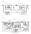
- the step-up/down power supply constituted using the bootstrap circuit is constituted by a step-down unit 1 , a step-up unit 2 , a control circuit 13 , a step-up/down determining circuit 14 , an inductor 9 , and an output capacity 121 .
- the step-down unit 1 is constituted by a switching element 3 , a step-down driver 4 , a bootstrap circuit 7 , and a diode 8 .
- the bootstrap circuit 7 is constituted by a diode 5 and a capacitor 6 .
- the step-up unit 2 is constituted by a switching element 11 , a step-up driver 12 , and a diode 10 .
- the switching element 3 or 11 is constituted by, for example, a transistor created by a semiconductor technique.
- the switching element 11 At the time of stepping-down when the input voltage Vin is high, the switching element 11 is continuously turned off, and the switching element 3 is switched.
- the switching element 3 When the switching element 3 is turned on, energy from the input voltage Vin is transferred to the output voltage Vo through the inductor 9 .
- current Iin flowing to the inductor 9 is accumulated in the inductor 9 as energy.
- the switching element 3 When the switching element 3 is turned off, the energy charged in the inductor 9 is transferred to the output voltage Vo through the diodes 8 and 10 . Accordingly, stepping-down is performed from the high input voltage Vin to the low output voltage Vo.
- the switching element 3 is continuously turned on, and the switching element 11 is switched.
- the input voltage Vin causes energy to be accumulated in the inductor 9 .
- the switching element 11 is turned off, the energy accumulated in the inductor 9 and energy from both sides of the input voltage Vin are transferred to the output voltage Vo through the diode 10 . Accordingly, stepping-up is performed from the low input voltage Vin to the high output voltage Vo.
- the step-up/down determining circuit 14 is a circuit that generates a high signal, for example, in a case in which the input voltage Vin is higher than the output voltage Vo, and generates a low signal in a case in which the input voltage Vin is lower than the output voltage Vo.
- the control circuit 13 is a circuit that generates control signals Vc_buck and Vc_boost by a signal Vchange generated by the step-up/down determining circuit 14 and a feedback signal from the output voltage Vo, controls the step-down unit 1 and the step-up unit 2 , and generates a stable output voltage Vo even when the input voltage Vin becomes lower or higher than the output voltage Vo to be required.
- the step-down driver 4 and the step-up driver 12 are circuits that receive the control signals Vc_buck and Vc_boost from the control circuit 13 , and drive the switching elements 3 and 11 to be turned on or off at a high speed.
- the switching element 3 of the step-down unit 1 is continuously turned on by the control signals Vc_buck and Vc_boost from the control circuit 13 , the switching element 11 of the step-up unit 2 is switched, and the output voltage Vo is stepped-up to a required voltage.
- the switching element 3 of the step-down unit 1 is switched by the control signals Vc_buck and Vc_boost from the control circuit 13 , the switching element 11 of the step-up unit 2 is continuously turned off, and the output voltage Vo is stepped-down to a required voltage.
- the gate voltage Vg of the switching element 3 is required a sufficient voltage higher than the drain voltage Vd.
- the drain voltage Vd of the switching element 3 is the input voltage Vin so as to become the highest voltage in the circuits.
- the bootstrap circuit fully turns on the switching element 3 , and generates a higher voltage than the input voltage Vin.
- the diode 8 When the switching element 3 is turned off, the diode 8 is conducted, and the source voltage Vs of the switching element 3 becomes substantially a GND voltage. At this time, the input voltage Vin charges the capacitor 6 through the diode 5 of the bootstrap circuit 7 , and a voltage Vb between the capacitor 6 and the diode 5 becomes an input voltage Vin ⁇ Vf.
- Vf is a forward voltage of the diode 5 .
- the source voltage Vs is substantially the same level as the drain voltage Vd, that is, the input voltage Vin, and thus the other end voltage of the capacitor 6 increases to the input voltage Vin. Accordingly, when the switching element 3 is turned on, the voltage Vb between the capacitor 6 and the diode 5 can be increased to 2Vin ⁇ Vf.
- This voltage Vb becomes a power supply voltage of the step-down driver 4 , and becomes the gate voltage Vg when the switching element 3 is turned on. Accordingly, it is possible to fully turn on the switching element 3 .
- a problem of the step-up/down power supply of FIG. 1 is that a circuit area is larger than as that in a case of only step-down power supply. Accordingly, costs of the power supply circuit increase. Reasons thereof are two as follows.
- Peak values Iin_boost and Iin_buck of the current Iin flowing to the switching element 3 at the time of stepping-up and stepping-down are obtained by Expressions (1) and (2) as follows.
- Iin_boost at the time of stepping-up is a multiple of Vo/Vin_boost of Iin_buck at the time of stepping-down.
- on-resistance of the switching element 3 at the time of stepping-up is needed to be a multiple of Vin_boost/Vo at the time of stepping-down
- an area of the switching element 3 of the step-up/down power supply is needed to be a multiple of Vo/Vin_boost in a case of only the step-down power supply. Since the input voltage Vin_boost at the time of stepping-up is lower than the output voltage Vo, the area of the switching element 3 of the step-up/down power supply is larger than that in the case of only the step-down power supply.
- Vin_boost input voltage at the time of stepping-up
- Vin_buck input voltage at the time of stepping-down
- Vf forward voltage value of diode of bootstrap circuit
- the gate voltages Vg_boost and Vg_buck which are generated by the bootstrap circuit, when the switching element 3 is turned on at the time of stepping-up and down become Vin_boost ⁇ 2 ⁇ Vf and Vin buck ⁇ 2 ⁇ Vf.
- a source-drain voltage Vds at the time of stepping-up and down is required to be the same.
- the drain voltages Vd_boost and Vd_buck of the switching element 3 at the time of stepping-up and down are Vin_boost and Vin_buck, and thus the source voltages Vs_boost and Vs_buck become Vin_boost-Vds and Vin_buck-Vds.
- a gate-source voltages Vgs_boost and Vgs_buck of the switching element 3 at the time of stepping-up and down become (Vin_boost ⁇ Vf+Vds) and (Vin_buck ⁇ Vf+Vds). Since the on-resistance of MOS is proportional to the gate-source voltage so that the same on-resistance is realized, the area of the switching element 3 of the step-up/down power supply is needed to be a multiple of (Vin_buck ⁇ Vf+Vds)/(Vin_boost ⁇ Vf+Vds) in the case of only the step-down power supply.
- the area of the switching element 3 of the step-up/down power supply is larger than that in the case of only the step-down power supply.
- the area of the switching element 3 of the step-up/down power supply is needed to be larger than that in the case of only the step-down power supply.
- the area of the switching element 3 is increased, a circuit area of the power supply is increased, and thus costs of the power supply circuit are increased.
- the bootstrap circuit 7 in the step-down unit 1 can be replaced to a charge pump circuit for increasing a voltage by combining a capacitor and a switch, but when the step-up/down power supply is stepped-down, the switching element 3 is needed to be switched at a high speed, and thus the charge pump circuit having a sufficient high current driving capability is required to be used. Accordingly, an area of the charge pump circuit becomes significantly large, the circuit area of the power supply, and costs of the power supply circuit are increased.
- An object of the invention is to provide a step-up/down power supply including a small circuit area.
- a step-up/down power supply including a step-down unit that generates an output voltage lower than an input voltage by turning on or off a step-down switch in which the input voltage of the step-up/down power supply is applied to an end of the step-down switch, a step-up unit that generates an output voltage higher than the input voltage by turning on or off a step-up switch in which a ground is applied to an end of the step-down switch, and a step-down gate voltage control circuit that controls a gate voltage of the step-down switch.
- the step-down gate voltage control circuit includes a gate voltage generating circuit that generates a first voltage and a second voltage for turning on the step-down switch, and a gate voltage switching circuit that switches between the first voltage and the second voltage, and the gate voltage generating circuit includes a first voltage source that generates the first voltage and a second generation voltage source that generates the second voltage.
- a step-up/down power supply including a step-down unit that generates an output voltage lower than an input voltage by turning on or off a step-down switch in which the input voltage of the step-up/down power supply is applied to an end of the step-down switch, a step-up unit that generates an output voltage higher than the input voltage by turning on or off a step-up switch in which a ground is applied to an end of the step-down switch, and a step-down gate voltage control circuit that controls a gate voltage of the step-down switch.
- the step-down gate voltage control circuit includes a gate voltage generating circuit that generates a first voltage and a second voltage for turning on the step-down switch, and a gate voltage switching circuit that switches between the first voltage and the second voltage, the gate voltage generating circuit includes a first generating circuit generating the first voltage and a second generating circuit generating the second voltage, and a load current for driving the second generating circuit is greater than that of the first generating circuit.
- a step-up/down power supply circuit that generates an output voltage from an input voltage, including a step-up unit that steps-up the input voltage, and a step-down unit that steps-down the input voltage, the step-down unit including a step-down switch constituted by a semiconductor transistor in which the input voltage is supplied to a first terminal of the semiconductor transistor, and a step-down gate voltage control circuit which switches between a first circuit having a different output voltage level and a second circuit different from the first circuit and supplies a gate voltage of the step-down switch.
- the step-down switch is continuously turned on at the time of a step-up operation for generating the output voltage higher than the input voltage, and the step-down switch is operated to be switched at the time of a step-down operation for generating the output voltage lower than the input voltage.
- the step-down gate voltage control circuit supplies a voltage of a first level from the first circuit as the gate voltage of the step-down switch at the time of the step-up operation, and supplies a voltage of a second level lower than the first level as the gate voltage of the step-down switch from the second circuit different from the first circuit at the time of the step-down operation.
- the step-down switch is continuously turned on at the time of a step-up operation for generating the output voltage higher than the input voltage, the step-down switch is operated to be switched at the time of a step-down operation for generating the output voltage lower than the input voltage.
- the step-down gate voltage control circuit supplies the gate voltage of the step-down switch from a charge pump circuit which is the first circuit at the time of the step-up operation, and supplies the gate voltage of the step-down switch from a bootstrap circuit which is the second circuit at the time of the step-down operation.
- an inductor is connected to a second terminal of the step-down switch
- the step-up unit includes a step-up switch, a first terminal of the step-up switch is connected to a ground potential, a second terminal is connected to the inductor, and a connection point of the second terminal and the inductor is connected to an output terminal for obtaining the output voltage
- the power supply circuit further includes a control circuit that controls operations of the step-down switch and the step-up switch.
- the control circuit controls the step-down switch so as to perform a switching operation and continuously turns off the step-up switch, at the time of the step-down operation for generating the output voltage lower than the input voltage, and controls the step-up switch so as to perform the switching operation and continuously turns on the step-down switch, at the time of the step-up operation for generating the output voltage higher than the input voltage.
- the step-down gate voltage control circuit supplies the gate voltage of the step-down switch from the charge pump circuit which is the first circuit at the time of the step-up operation, and supplies the gate voltage of the step-down switch from the bootstrap circuit which is the second circuit at the time of the step-down operation.
- the second circuit supplies the voltage of the second level lower than the first level as the gate voltage of the step-down switch, and the second circuit has higher current driving capability and a lower output voltage level than that of the first circuit.
- the first circuit and the second circuit independently input and output a voltage.
- FIG. 1 is a circuit diagram illustrating a configuration example of a step-up/down power supply.
- FIG. 2 is a circuit diagram illustrating a configuration of the step-up/down power supply of Embodiment 1.
- FIG. 3 is a timing chart of switching between stepping-up and stepping-down of the step-up/down power supply of Embodiment 1.
- FIG. 4 is a flow chart of a switching operation of the step-up/down power supply of Embodiment 1 from stepping-down to stepping-up.
- FIG. 5 is a flow chart of a switching operation of the step-up/down power supply of Embodiment 1 from stepping-up to stepping-down.
- a notation such as a “first”, a “second”, or a “third” in this specification is attached to identify a configuration element, and is not necessary to limit to the numeral or an order.
- the numeral for identifying the configuration element is used in each context, and the numeral used for one context is not necessary to limit to indicating the same configuration in other contexts.
- it does not preclude the configuration element identified by a certain numeral from serving as a function of a configuration element identified by another numeral.
- a power supply voltage of a driver of a switching element 3 is generated by switching between a bootstrap circuit and a charge pump circuit.
- step-up/down determining circuit determines that the input voltage Vin becomes lower than the output voltage Vo, a power supply is in a step-up mode, and the switching element 3 is continuously turned on.
- the power supply voltage of the driver of the switching element 3 is switched from the bootstrap circuit to the charge pump circuit by a voltage switching circuit at this timing.
- the step-up/down determining circuit determines that the input voltage Vin becomes higher than the output voltage Vo, the power supply is in a step-down mode, and the switching element 3 is switched.
- the power supply voltage of the driver of the switching element 3 is switched from the charge pump circuit to the bootstrap circuit by the voltage switching circuit at this timing.
- FIG. 2 is a diagram illustrating a configuration of a step-up/down power supply of Embodiment 1. The same numeral is given to the same configuration part in FIGS. 2 and 1 .
- the step-up/down power supply of Embodiment 1 is constituted by a step-down unit 15 , a step-up unit 2 , a control circuit 13 , a step-up/down determining circuit 14 , an inductor 9 , and an output capacity 121 . Since the step-up unit 2 , the control circuit 13 , the step-up/down determining circuit 14 , the inductor 9 , the output capacity 121 are the same as those of FIG. 1 , description thereof will be omitted.
- the step-down unit 15 is constituted by a switching element 23 , a diode 8 , a step-down driver 24 , a voltage switching circuit 16 , and a gate voltage generating circuit 22 .
- the gate voltage generating circuit 22 is constituted by a charge pump (CP) circuit 21 and a bootstrap circuit 7 . Since the bootstrap circuit 7 is the same as that of FIG. 1 , description thereof will be omitted.
- the charge pump (CP) circuit 21 is constituted by a charge pump (CP) initiation determining circuit 17 , an oscillator 19 , a charge pump (CP) 18 , and a charge pump (CP) voltage determining circuit 20 .
- the charge pump circuit 21 a known electronic circuit for increasing a voltage can be used by combining the capacitor and the switch.
- the oscillator 19 a known configuration can be also used.
- the bootstrap circuit 7 a known electronic circuit constituted by a capacitor and a diode can be used.
- FIG. 2 illustrates an example, but it is not limited to this configuration.
- the charge pump circuit 21 and the bootstrap circuit 7 are separately and independently configured, and input or output is also independent.
- Each of output voltages Vcp and Vb is input to the voltage switching circuit 16 , and either of the output voltages is selected and supplied to the step-down driver 24 .
- Embodiment 1 At the time of stepping-up and down, the entire operations of the step-up/down power supply of Embodiment 1 will be described as follows.
- the switching element 11 is continuously turned off, and the switching element 23 is switched.
- the switching element 23 is turned on, energy is transferred to the output voltage Vo from the input voltage Vin through the inductor 9 .
- a current flowing to the inductor 9 is accumulated in the inductor 9 as energy.
- the switching element 23 is turned off, the energy charged in the inductor 9 is transferred to the output voltage Vo through the diode 8 . Accordingly, stepping-down is performed from a high input voltage Vin to a low output voltage Vo.
- the switching element 23 is continuously turned on, and the switching element 11 is switched.
- the switching element 11 is turned on, the input voltage Vin is accumulated in the inductor 9 as energy.
- the switching element 11 is turned off, the energy charged in the inductor 9 and energy from both sides of the input voltage Vin are transferred to the output voltage Vo through the diode 10 . Accordingly, stepping-up is performed from a low input voltage Vin to a high output voltage Vo.
- the gate voltage generating circuit 22 generates two types of voltages of a charge pump voltage Vcp generated by the charge pump (CP) circuit 21 and a bootstrap voltage Vb generated by the bootstrap circuit 7 . Since an operation of the bootstrap circuit 7 is the same as FIG. 1 , description thereof will be omitted.
- the charge pump (CP) initiation determining circuit 17 controls switching of an operation state (stop, initiating, and operating) of the oscillator 19 by a determining signal Vst which is generated depending on a magnitude of the input voltage Vin and a determining signal Vchange output from the step-up/down determining circuit 14 .
- the oscillator 19 generates a pulse signal Vosc.
- the charge pump (CP) 18 is a circuit for increasing a voltage by combining a plurality of capacitors and a plurality of switches, and generates a high voltage Vcp from the input voltage Vin by the pulse signal Vosc from the oscillator 19 .
- the charge pump (CP) voltage determining circuit 20 generates a determining signal Vcptest if the output voltage Vcp of the charge pump (CP) 18 becomes a desired voltage, and inputs the determining signal to the voltage switching circuit 16 .
- the voltage switching circuit 16 outputs the bootstrap voltage Vb and the charge pump voltage Vcp which are input in a switching manner as a power supply voltage Vdriver of the step-down driver 16 depending on the determining signal Vcptest from the charge pump (CP) voltage determining circuit 20 and the determining signal Vchange from the step-up/down determining circuit 14 .
- the step-down driver 24 is a circuit which receives a control signal Vc_buck of the control circuit 13 and drives the switching element 23 so as to be turned on and off at a high speed.
- the gate voltage Vg causing the switching element 23 to be turned on becomes an output of the voltage switching circuit 16 , that is, the power supply voltage Vdriver of the step-down driver 24 .
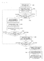
- FIG. 3 is a timing chart of each signal and an output voltage when the step-up/down power supply of Embodiment 1 is switched from stepping-down and stepping-up.
- FIGS. 4 and 5 are respectively an operation flow of switching from stepping-down to stepping-up and an operation flow of switching from stepping-up to stepping-down of the step-up/down power supply of Embodiment 1.
- An operation of the oscillator 19 is initiated by the determining signal Vst, generation of the pulse signal Vosc is started (S 405 ), and the output voltage Vcp of the charge pump (CP) 18 is increased (S 406 ).
- the determining signal Vcptest output from the output of the charge pump (CP) voltage determining circuit 20 becomes high from low, and the state 302 of the charge pump (CP) circuit 21 becomes the operation state from the initiating state (S 408 ).
- the operation state 301 of the step-up/down power supply is switched from stepping-down to stepping-up by the control circuit 13 (S 411 ).
- the bootstrap circuit 7 since the bootstrap circuit 7 is continuously operated even after being switched to be output from the charge pump (CP) 18 , the output voltage Vb 309 of the bootstrap circuit 7 does not become zero, but the output is decreased as the input voltage Vin 303 is decreased.
- the bootstrap circuit 7 may be configured to be stopped to be operated after being switched to be output from the charge pump (CP) 18 , but in this case, an initiation timing of the bootstrap circuit is needed to be considered.
- the determining signal Vchange 308 output from the step-up/down determining circuit 14 becomes low from high.
- the operation state 301 of the step-up/down power supply is switched from stepping-up to stepping-down by the control circuit 13 (S 505 ).
- the charge pump (CP) initiation determining circuit 17 is reset, and a determining signal Vst 304 of an output is switched from high to low (S 506 ).
- a state of the oscillator 19 becomes a stop state from an operation state by the determining signal Vst, and the pulse signal Vosc 305 is stopped to be generated (S 507 ). Accordingly, the output voltage Vcp 306 of the charge pump (CP) 18 decreases (S 508 ).
- the determining signal Vcptest 307 output from the charge pump (CP) voltage determining circuit 20 becomes low from high, and the state 302 of the charge pump (CP) circuit 21 becomes a stop state from the operation state (S 509 ).
- the threshold Vth 1 in the charge pump (CP) initiation determining circuit 17 be set to be higher than the threshold Vth 3 in the step-up/down determining
- the threshold Vth 3 in the step-up/down determining circuit 14 is a value required to switch the operation state of the step-up/down power supply between a stepping up state and a stepping-down state depending on a magnitude relationship of the input voltage Vin and a desired output voltage Vo.
- the threshold Vth 3 in the step-up/down determining circuit 14 may be set to be the same as the desired output voltage Vo.
- the threshold Vth 1 in the charge pump (CP) initiation determining circuit 17 is determined depending on the initiating time of the charge pump (CP) circuit 21 , a maximum decrease speed of the input voltage Vin 303 , and the threshold Vth 3 in the step-up/down determining circuit 14 .
- the threshold Vth 1 in the charge pump (CP) initiation determining circuit 17 becomes Vth 3 +A ⁇ B.
- the threshold Vth 2 in the charge pump (CP) voltage determining circuit 20 is a value of the output voltage Vcp 306 of the desired charge pump (CP) 18 , and is desirably set to be higher than both the threshold Vth 1 in the charge pump (CP) initiation determining circuit 17 and the threshold Vth 3 in the step-up/down determining circuit 14 .
- the value of the output voltage Vcp 306 of the desired charge pump (CP) 18 is obtained with reference to description as follows.
- the area of the switching element 3 is larger than that in the case of only the step-down power supply.
- An input current Iin_boost at the time of stepping-up is a multiple of Vo/Vin_boost of Iin_buck at the time of stepping-down. Therefore, in order to realize the same efficiency, the area of the switching element 3 is needed to be a multiple of Vo/Vin_boost in the case of only the step-down power supply.
- the area of the switching element 3 is needed to be multiplied by 1.2 of the case of only the step-down power supply.
- the area of the switching element 3 is needed to be multiplied by 1.4 of the case of only the step-down power supply.
- Vd_boost of the switching element 3 at the time of stepping-up is Vin_boost (5V)
- a value of the output voltage Vcp 306 of the desired charge pump (CP) 18 of the step-up/down power supply in FIG. 2 of Embodiment 1 is needed to be 15.42 V. This value becomes the threshold Vth 2 in the charge pump (CP) voltage determining circuit 20 .
- an area of the switching element 23 is possible to be the same as that in the case of only the step-down power supply. Accordingly, an increase of costs of the step-up/down power supply can be suppressed.
- the switching element 3 is continuously turned on.
- the gate voltage causing the switching element 3 to be continuously turned on is generated by the charge pump circuit. Since the switching element 3 is driven to be turned on by a higher voltage than the voltage generated from the bootstrap circuit of FIG. 1 , the area of the switching element 3 can be reduced.
- the bootstrap circuit a circuit of which a current driving capability is high and an output voltage level is low
- the charge pump circuit a circuit of which a current driving capability is low and an output voltage level is high are appropriately used at the time of stepping-up and down.
- the step-down switch 23 (transistor) is needed to be continuously turned on.
- a decreasing power supply (for example, battery) voltage is increased to a voltage required for a gate voltage of the transistor by the bootstrap circuit, in order to satisfy requirement of the on-resistance at the time of stepping-up, the area of the step-down switch 23 is needed to be large.
- the charge pump circuit is capable of supplying a sufficient gate voltage for continuously turning on the transistor (step-down switch 23 ) at the time of stepping-up.
- step-down switch 23 transistor
- the current driving capability is needed to be increased in the charge pump circuit. Therefore, a large capacity external capacitor is needed. Meanwhile, the bootstrap circuit has the low output voltage level, but may become a problem at the time of stepping-down when the power supply (for example, battery) voltage is high. Further, since the sufficient current driving capability for switching the transistor (step-down switch 23 ) at the time of stepping-down is included, the capacitor is not needed to be large.
- the step-down switch 23 may be configured to use a first switching element and a second switching element having a smaller element area than that of the first switching element which are connected in parallel.
- the first switching element is turned on by the voltage of the charge pump circuit 18
- the second switching element is turned on by the voltage of the bootstrap circuit 7 . Switching characteristics suitable for at the time of stepping-up and down are obtained.
- the invention is not limited to the above-described embodiments, and includes various modification examples. For example, it is possible to replace a part of a configuration of one example with a configuration of another example, and also to add the configuration of one example to the configuration of another example. In addition, it is possible to add, delete, or replace the configuration of another example with respect to the part of the configuration of each example.
- a function of the “source” or “drain” of the transistor is changed in a case in which a transistor having different polarity is adopted, a case a direction of a current is changed in a circuit operation, or the like. Therefore, in this specification, a term of the “source” or “drain” can be used by being changed.
- the invention relates to the switching power supply, and more particularly, it is possible to be used for an on-vehicle step-up/down power supply that generates a voltage for a micro-computer, or the like.
Abstract
Description
At the time of stepping-up Iin_boost=Vo·Io/Vin_boost Expression (1)
At the time of stepping-down Iin_buck=Io Expression (2)
Vg=Vin·2−Vf Expression (3)
Claims (7)
Applications Claiming Priority (3)
| Application Number | Priority Date | Filing Date | Title |
|---|---|---|---|
| JP2015-225628 | 2015-11-18 | ||
| JP2015225628A JP6490565B2 (en) | 2015-11-18 | 2015-11-18 | Buck-boost power supply and power supply circuit |
| PCT/JP2016/078566 WO2017086028A1 (en) | 2015-11-18 | 2016-09-28 | Step-up/down power supply and power supply circuit |
Publications (2)
| Publication Number | Publication Date |
|---|---|
| US20180316268A1 US20180316268A1 (en) | 2018-11-01 |
| US10340799B2 true US10340799B2 (en) | 2019-07-02 |
Family
ID=58718686
Family Applications (1)
| Application Number | Title | Priority Date | Filing Date |
|---|---|---|---|
| US15/772,128 Expired - Fee Related US10340799B2 (en) | 2015-11-18 | 2016-09-28 | Step-up/down power supply and power supply circuit |
Country Status (5)
| Country | Link |
|---|---|
| US (1) | US10340799B2 (en) |
| JP (1) | JP6490565B2 (en) |
| CN (1) | CN108352784B (en) |
| DE (1) | DE112016004754T5 (en) |
| WO (1) | WO2017086028A1 (en) |
Families Citing this family (4)
| Publication number | Priority date | Publication date | Assignee | Title |
|---|---|---|---|---|
| FR3064849B1 (en) * | 2017-03-31 | 2019-06-07 | Centum Adetel Transportation | HYBRID POWER CELL |
| US10714152B1 (en) * | 2019-05-29 | 2020-07-14 | Advanced Micro Devices, Inc. | Voltage regulation system for memory bit cells |
| CN110299842B (en) * | 2019-07-23 | 2024-02-13 | 东莞保力电子有限公司 | Boost freewheel low pressure differential Buck type switching power supply device |
| US11829222B2 (en) | 2020-09-25 | 2023-11-28 | Advanced Micro Devices, Inc. | Operating voltage adjustment for aging circuits |
Citations (10)
| Publication number | Priority date | Publication date | Assignee | Title |
|---|---|---|---|---|
| JPH1023749A (en) | 1996-07-03 | 1998-01-23 | Fuji Electric Co Ltd | Switching power unit |
| JP2002037099A (en) | 2000-07-24 | 2002-02-06 | Koyo Seiko Co Ltd | Electronic control device for electric power, steering |
| JP2006033971A (en) | 2004-07-14 | 2006-02-02 | Sanyo Electric Co Ltd | Power supply circuit |
| JP2008029085A (en) | 2006-07-19 | 2008-02-07 | Denso Corp | Drive unit for switching device and switching constant-voltage power supply unit |
| US7737668B2 (en) * | 2007-09-07 | 2010-06-15 | Panasonic Corporation | Buck-boost switching regulator |
| JP2012182884A (en) | 2011-02-28 | 2012-09-20 | Denso Corp | Load drive control circuit |
| US20140252950A1 (en) * | 2013-03-07 | 2014-09-11 | Panasonic Corporation | Semiconductor light source lighting circuit and vehicular lamp |
| US20150289325A1 (en) * | 2014-04-03 | 2015-10-08 | Linear Technology Corporation | Boost then floating buck mode converter for led driver using common switch control signal |
| US20150314754A1 (en) * | 2012-12-11 | 2015-11-05 | Denso Corporation | Vehicular emergency reporting device |
| US20170036555A1 (en) * | 2015-08-05 | 2017-02-09 | GM Global Technology Operations LLC | Transformerless, current-isolated onboard charger with solid-state switching controls |
Family Cites Families (4)
| Publication number | Priority date | Publication date | Assignee | Title |
|---|---|---|---|---|
| ITMI20022268A1 (en) * | 2002-10-25 | 2004-04-26 | Atmel Corp | VARIABLE CHARGE PUMP CIRCUIT WITH DYNAMIC LOAD |
| US7313004B1 (en) * | 2006-12-21 | 2007-12-25 | System General Corp. | Switching controller for resonant power converter |
| JP2014011841A (en) * | 2012-06-28 | 2014-01-20 | Denso Corp | Switching regulator |
| CN104953991A (en) * | 2015-06-23 | 2015-09-30 | 东南大学 | IGBT (insulated gate bipolar transistor) drive circuit provided with level bootstrap and charge pump circuits and adopting double N-MOSFET (N-channel metal oxide semiconductor field effect transistor) drive stages as well as sequential control method |
-
2015
- 2015-11-18 JP JP2015225628A patent/JP6490565B2/en not_active Expired - Fee Related
-
2016
- 2016-09-28 DE DE112016004754.1T patent/DE112016004754T5/en not_active Withdrawn
- 2016-09-28 WO PCT/JP2016/078566 patent/WO2017086028A1/en active Application Filing
- 2016-09-28 US US15/772,128 patent/US10340799B2/en not_active Expired - Fee Related
- 2016-09-28 CN CN201680066564.2A patent/CN108352784B/en not_active Expired - Fee Related
Patent Citations (11)
| Publication number | Priority date | Publication date | Assignee | Title |
|---|---|---|---|---|
| JPH1023749A (en) | 1996-07-03 | 1998-01-23 | Fuji Electric Co Ltd | Switching power unit |
| JP2002037099A (en) | 2000-07-24 | 2002-02-06 | Koyo Seiko Co Ltd | Electronic control device for electric power, steering |
| JP2006033971A (en) | 2004-07-14 | 2006-02-02 | Sanyo Electric Co Ltd | Power supply circuit |
| JP2008029085A (en) | 2006-07-19 | 2008-02-07 | Denso Corp | Drive unit for switching device and switching constant-voltage power supply unit |
| US7737668B2 (en) * | 2007-09-07 | 2010-06-15 | Panasonic Corporation | Buck-boost switching regulator |
| JP2012182884A (en) | 2011-02-28 | 2012-09-20 | Denso Corp | Load drive control circuit |
| US20150314754A1 (en) * | 2012-12-11 | 2015-11-05 | Denso Corporation | Vehicular emergency reporting device |
| US20140252950A1 (en) * | 2013-03-07 | 2014-09-11 | Panasonic Corporation | Semiconductor light source lighting circuit and vehicular lamp |
| JP2014175124A (en) | 2013-03-07 | 2014-09-22 | Koito Mfg Co Ltd | Semiconductor light source lighting circuit and vehicular lighting fixture |
| US20150289325A1 (en) * | 2014-04-03 | 2015-10-08 | Linear Technology Corporation | Boost then floating buck mode converter for led driver using common switch control signal |
| US20170036555A1 (en) * | 2015-08-05 | 2017-02-09 | GM Global Technology Operations LLC | Transformerless, current-isolated onboard charger with solid-state switching controls |
Non-Patent Citations (1)
| Title |
|---|
| International Search Report of PCT/JP2016/078566 dated Dec. 27, 2016. |
Also Published As
| Publication number | Publication date |
|---|---|
| WO2017086028A1 (en) | 2017-05-26 |
| DE112016004754T5 (en) | 2018-07-05 |
| US20180316268A1 (en) | 2018-11-01 |
| CN108352784B (en) | 2020-03-06 |
| CN108352784A (en) | 2018-07-31 |
| JP2017099048A (en) | 2017-06-01 |
| JP6490565B2 (en) | 2019-03-27 |
Similar Documents
| Publication | Publication Date | Title |
|---|---|---|
| US9484758B2 (en) | Hybrid bootstrap capacitor refresh technique for charger/converter | |
| KR101036867B1 (en) | Dc-dc converter | |
| US7388422B2 (en) | Charge pump circuit for high side drive circuit and driver driving voltage circuit | |
| US10340799B2 (en) | Step-up/down power supply and power supply circuit | |
| US10879802B2 (en) | DC-DC converter and display apparatus having the same | |
| US8415932B2 (en) | Switching control circuit | |
| US7528589B2 (en) | Step-up DC/DC converter and electronic appliance therewith | |
| JP2007215259A (en) | Drive circuit and switching regulator using the same | |
| US20160011610A1 (en) | Dc-dc converter and television receiver therewith | |
| US20140062431A1 (en) | Dc-dc converter and semiconductor device | |
| US20140176105A1 (en) | Electronic control device including voltage converter | |
| JP2012205408A (en) | Power circuit | |
| JP2008295237A (en) | Switching pulse formation circuit and regulator using same | |
| US9590508B2 (en) | Control apparatus, and control method for buck-boost power supply with two primary switches | |
| US9992826B1 (en) | Dual mode constant current LED driver | |
| JP2014011841A (en) | Switching regulator | |
| US9351361B2 (en) | Driver circuit for light-emitting diodes | |
| US10362645B1 (en) | Negative charge pump doubling output voltage range for step-up LED driver | |
| US20220200458A1 (en) | Power supply for driving synchronous rectification elements of sepic converter | |
| US20130162234A1 (en) | Buck regulation of a boost regulator | |
| JP6500701B2 (en) | Drive power circuit | |
| TWI405392B (en) | Voltage converter | |
| JP6559901B2 (en) | Electronic control unit | |
| US11641162B2 (en) | Circuits and methods for generating a supply voltage for a switching regulator | |
| CN113615059A (en) | Detection of low output voltage of power converter |
Legal Events
| Date | Code | Title | Description |
|---|---|---|---|
| FEPP | Fee payment procedure |
Free format text: ENTITY STATUS SET TO UNDISCOUNTED (ORIGINAL EVENT CODE: BIG.); ENTITY STATUS OF PATENT OWNER: LARGE ENTITY |
|
| AS | Assignment |
Owner name: HITACHI AUTOMOTIVE SYSTEMS, LTD., JAPAN Free format text: ASSIGNMENT OF ASSIGNORS INTEREST;ASSIGNORS:LIU, MING;KAJIYAMA, SHINYA;YAMAWAKI, TAIZO;AND OTHERS;SIGNING DATES FROM 20180416 TO 20180524;REEL/FRAME:045933/0379 |
|
| STPP | Information on status: patent application and granting procedure in general |
Free format text: NOTICE OF ALLOWANCE MAILED -- APPLICATION RECEIVED IN OFFICE OF PUBLICATIONS |
|
| STPP | Information on status: patent application and granting procedure in general |
Free format text: PUBLICATIONS -- ISSUE FEE PAYMENT VERIFIED |
|
| STCF | Information on status: patent grant |
Free format text: PATENTED CASE |
|
| AS | Assignment |
Owner name: HITACHI ASTEMO, LTD., JAPAN Free format text: CHANGE OF NAME;ASSIGNOR:HITACHI AUTOMOTIVE SYSTEMS, LTD.;REEL/FRAME:056299/0447 Effective date: 20210101 |
|
| FEPP | Fee payment procedure |
Free format text: MAINTENANCE FEE REMINDER MAILED (ORIGINAL EVENT CODE: REM.); ENTITY STATUS OF PATENT OWNER: LARGE ENTITY |
|
| LAPS | Lapse for failure to pay maintenance fees |
Free format text: PATENT EXPIRED FOR FAILURE TO PAY MAINTENANCE FEES (ORIGINAL EVENT CODE: EXP.); ENTITY STATUS OF PATENT OWNER: LARGE ENTITY |
|
| STCH | Information on status: patent discontinuation |
Free format text: PATENT EXPIRED DUE TO NONPAYMENT OF MAINTENANCE FEES UNDER 37 CFR 1.362 |
|
| FP | Lapsed due to failure to pay maintenance fee |
Effective date: 20230702 |