US10340468B2 - Display device - Google Patents
Display device Download PDFInfo
- Publication number
- US10340468B2 US10340468B2 US15/698,739 US201715698739A US10340468B2 US 10340468 B2 US10340468 B2 US 10340468B2 US 201715698739 A US201715698739 A US 201715698739A US 10340468 B2 US10340468 B2 US 10340468B2
- Authority
- US
- United States
- Prior art keywords
- film
- base film
- region
- display device
- display
- Prior art date
- Legal status (The legal status is an assumption and is not a legal conclusion. Google has not performed a legal analysis and makes no representation as to the accuracy of the status listed.)
- Active
Links
Images


Classifications
-
- H—ELECTRICITY
- H10—SEMICONDUCTOR DEVICES; ELECTRIC SOLID-STATE DEVICES NOT OTHERWISE PROVIDED FOR
- H10K—ORGANIC ELECTRIC SOLID-STATE DEVICES
- H10K71/00—Manufacture or treatment specially adapted for the organic devices covered by this subclass
- H10K71/80—Manufacture or treatment specially adapted for the organic devices covered by this subclass using temporary substrates
-
- H01L51/0097—
-
- H01L51/5253—
-
- H—ELECTRICITY
- H10—SEMICONDUCTOR DEVICES; ELECTRIC SOLID-STATE DEVICES NOT OTHERWISE PROVIDED FOR
- H10K—ORGANIC ELECTRIC SOLID-STATE DEVICES
- H10K50/00—Organic light-emitting devices
- H10K50/80—Constructional details
- H10K50/84—Passivation; Containers; Encapsulations
- H10K50/844—Encapsulations
-
- H—ELECTRICITY
- H10—SEMICONDUCTOR DEVICES; ELECTRIC SOLID-STATE DEVICES NOT OTHERWISE PROVIDED FOR
- H10K—ORGANIC ELECTRIC SOLID-STATE DEVICES
- H10K59/00—Integrated devices, or assemblies of multiple devices, comprising at least one organic light-emitting element covered by group H10K50/00
- H10K59/80—Constructional details
- H10K59/87—Passivation; Containers; Encapsulations
- H10K59/873—Encapsulations
-
- H—ELECTRICITY
- H10—SEMICONDUCTOR DEVICES; ELECTRIC SOLID-STATE DEVICES NOT OTHERWISE PROVIDED FOR
- H10K—ORGANIC ELECTRIC SOLID-STATE DEVICES
- H10K77/00—Constructional details of devices covered by this subclass and not covered by groups H10K10/80, H10K30/80, H10K50/80 or H10K59/80
- H10K77/10—Substrates, e.g. flexible substrates
- H10K77/111—Flexible substrates
-
- H01L2227/323—
-
- H01L2227/326—
-
- H01L2251/5338—
-
- H01L27/323—
-
- H01L27/3276—
-
- H—ELECTRICITY
- H10—SEMICONDUCTOR DEVICES; ELECTRIC SOLID-STATE DEVICES NOT OTHERWISE PROVIDED FOR
- H10K—ORGANIC ELECTRIC SOLID-STATE DEVICES
- H10K2102/00—Constructional details relating to the organic devices covered by this subclass
- H10K2102/301—Details of OLEDs
- H10K2102/311—Flexible OLED
-
- H—ELECTRICITY
- H10—SEMICONDUCTOR DEVICES; ELECTRIC SOLID-STATE DEVICES NOT OTHERWISE PROVIDED FOR
- H10K—ORGANIC ELECTRIC SOLID-STATE DEVICES
- H10K59/00—Integrated devices, or assemblies of multiple devices, comprising at least one organic light-emitting element covered by group H10K50/00
- H10K59/10—OLED displays
- H10K59/12—Active-matrix OLED [AMOLED] displays
- H10K59/1201—Manufacture or treatment
-
- H—ELECTRICITY
- H10—SEMICONDUCTOR DEVICES; ELECTRIC SOLID-STATE DEVICES NOT OTHERWISE PROVIDED FOR
- H10K—ORGANIC ELECTRIC SOLID-STATE DEVICES
- H10K59/00—Integrated devices, or assemblies of multiple devices, comprising at least one organic light-emitting element covered by group H10K50/00
- H10K59/10—OLED displays
- H10K59/12—Active-matrix OLED [AMOLED] displays
- H10K59/131—Interconnections, e.g. wiring lines or terminals
-
- H—ELECTRICITY
- H10—SEMICONDUCTOR DEVICES; ELECTRIC SOLID-STATE DEVICES NOT OTHERWISE PROVIDED FOR
- H10K—ORGANIC ELECTRIC SOLID-STATE DEVICES
- H10K59/00—Integrated devices, or assemblies of multiple devices, comprising at least one organic light-emitting element covered by group H10K50/00
- H10K59/40—OLEDs integrated with touch screens
-
- Y—GENERAL TAGGING OF NEW TECHNOLOGICAL DEVELOPMENTS; GENERAL TAGGING OF CROSS-SECTIONAL TECHNOLOGIES SPANNING OVER SEVERAL SECTIONS OF THE IPC; TECHNICAL SUBJECTS COVERED BY FORMER USPC CROSS-REFERENCE ART COLLECTIONS [XRACs] AND DIGESTS
- Y02—TECHNOLOGIES OR APPLICATIONS FOR MITIGATION OR ADAPTATION AGAINST CLIMATE CHANGE
- Y02E—REDUCTION OF GREENHOUSE GAS [GHG] EMISSIONS, RELATED TO ENERGY GENERATION, TRANSMISSION OR DISTRIBUTION
- Y02E10/00—Energy generation through renewable energy sources
- Y02E10/50—Photovoltaic [PV] energy
- Y02E10/549—Organic PV cells
-
- Y—GENERAL TAGGING OF NEW TECHNOLOGICAL DEVELOPMENTS; GENERAL TAGGING OF CROSS-SECTIONAL TECHNOLOGIES SPANNING OVER SEVERAL SECTIONS OF THE IPC; TECHNICAL SUBJECTS COVERED BY FORMER USPC CROSS-REFERENCE ART COLLECTIONS [XRACs] AND DIGESTS
- Y02—TECHNOLOGIES OR APPLICATIONS FOR MITIGATION OR ADAPTATION AGAINST CLIMATE CHANGE
- Y02P—CLIMATE CHANGE MITIGATION TECHNOLOGIES IN THE PRODUCTION OR PROCESSING OF GOODS
- Y02P70/00—Climate change mitigation technologies in the production process for final industrial or consumer products
- Y02P70/50—Manufacturing or production processes characterised by the final manufactured product
Definitions
- An embodiment of the present invention relates to a display device such as an organic EL display device and a liquid crystal display device and a manufacturing method thereof.
- a display device such as an organic EL display device and a liquid crystal display device and a manufacturing method thereof.
- an embodiment of the present invention relates to a flexible display device and a manufacturing method thereof.
- a liquid crystal display device and an organic EL (Electroluminescence) display device having a liquid crystal element or a light-emitting element in each pixel are represented as a typical example of a display device.
- These display devices have a liquid crystal element or an organic light-emitting element (hereinafter, referred to as a light-emitting element) in each of a plurality of pixels formed over a substrate.
- a liquid crystal element and a light-emitting element respectively have a liquid crystal or a layer (hereinafter, referred to as an organic layer or an EL layer) including an organic compound between a pair of electrodes and are operated by applying a voltage or supplying current between the pair of electrodes.
- a flexible display device is called a sheet display and has attracted much attention as a wearable display device attachable to clothes or a part of a body, for example.
- Japanese patent application publication No. 2015-26055 discloses a display device utilizing, as a flexible substrate, a substrate including fibers containing silicon rubber and the like. This display device can be folded due to its flexibility.
- An embodiment of the present invention is a display device.
- the display device possesses a base film and a display-element layer over the base film, the display-element layer having a display region including a plurality of pixels.
- the base film has a first gap separating the base film into a first region and a second region.
- the display-element layer includes an insulating film, and the insulating film extends over the first region and the second region and overlaps with the first gap.
- An embodiment of the present invention is a display device.
- the display device possesses a first base film and a second base film separated from each other, and a display-element layer over the first base film and the second base film, the display-element layer having a display region including a plurality of pixels.
- the display-element layer has an insulating film, and the insulating film extends over the first base film and the second base film and overlaps with a boundary between the first base film and the second base film.
- An embodiment of the present invention is a manufacturing method of a display device.
- the manufacturing method includes: forming a base film over a first supporting substrate; forming a display-element layer over the base film, the display-element layer having a display region including a plurality of pixels; forming a cap film over a second supporting substrate; bonding the first supporting substrate to the second supporting substrate so that the base film, the display-element layer, and the cap film are sandwiched therebetween; separating the second supporting substrate from the cap film; bonding a second protection sheet to the cap film; separating the first supporting film from the base film; forming a gap in the base film to separate the base film into two parts; and bonding a first protection sheet to the base film.
- FIG. 1 is a schematic developed view of a display device according to an embodiment of the present invention
- FIG. 2 is a schematic side view of a display device according to an embodiment of the present invention.
- FIG. 3A and FIG. 3B are schematic side views of a display device according to an embodiment of the present invention.
- FIG. 4A and FIG. 4B are schematic side views of a display device according to an embodiment of the present invention.
- FIG. 5A to FIG. 5D are schematic top views of a display device according to an embodiment of the present invention.
- FIG. 6 is a schematic top view of a display device according to an embodiment of the present invention.
- FIG. 7 is a schematic top view of a display device according to an embodiment of the present invention.
- FIG. 8 is a schematic cross-sectional view showing an outline of a manufacturing method of a display device according to an embodiment of the present invention.
- FIG. 9 is a schematic cross-sectional view showing an outline of a manufacturing method of a display device according to an embodiment of the present invention.
- FIG. 10 is a schematic cross-sectional view showing an outline of a manufacturing method of a display device according to an embodiment of the present invention.
- FIG. 12 is a schematic cross-sectional view showing an outline of a manufacturing method of a display device according to an embodiment of the present invention.
- FIG. 13A to FIG. 13C are schematic cross-sectional views showing a manufacturing method of a display device according to an embodiment of the present invention.
- FIG. 14A to FIG. 14C are schematic cross-sectional views showing a manufacturing method of a display device according to an embodiment of the present invention.
- FIG. 15A and FIG. 15B are schematic cross-sectional views showing a manufacturing method of a display device according to an embodiment of the present invention.
- FIG. 16A and FIG. 16B are schematic cross-sectional views showing a manufacturing method of a display device according to an embodiment of the present invention.
- FIG. 17A and FIG. 17B are schematic cross-sectional views showing a manufacturing method of a display device according to an embodiment of the present invention.
- FIG. 18 is a schematic cross-sectional view showing a manufacturing method of a display device according to an embodiment of the present invention.
- FIG. 19 is a schematic cross-sectional view showing a manufacturing method of a display device according to an embodiment of the present invention.
- FIG. 20 is a schematic cross-sectional view showing a manufacturing method of a display device according to an embodiment of the present invention.
- FIG. 21A and FIG. 21B are schematic cross-sectional views showing a manufacturing method of a display device according to an embodiment of the present invention.
- FIG. 22 is a schematic cross-sectional view showing a manufacturing method of a display device according to an embodiment of the present invention.
- FIG. 23 is a schematic cross-sectional view showing a manufacturing method of a display device according to an embodiment of the present invention.
- FIG. 24 is a schematic cross-sectional view showing a manufacturing method of a display device according to an embodiment of the present invention.
- FIG. 25 is a schematic cross-sectional view showing a manufacturing method of a display device according to an embodiment of the present invention.
- FIG. 26 is a schematic cross-sectional view showing a manufacturing method of a display device according to an embodiment of the present invention.
- the plurality of films when a plurality of films is formed by performing etching or light irradiation on one film, the plurality of films may have functions or rules different from each other.
- the plurality of films originates from a film formed as the same layer in the same process and has the same layer structure and the same material. Therefore, the plurality of films is defined as films existing in the same layer.
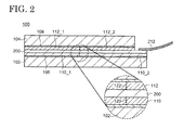
- FIG. 1 A schematic developed view of the display device 100 is shown in FIG. 1 .
- the display device 100 has a display-element layer 200 .
- a base film 110 and a cap film 112 are disposed under and over the display-element layer 200 , respectively, and the display-element layer 200 is sandwiched by the base film 110 and the cap film 112 .
- the display device 100 further possesses a first protection sheet 102 and a second protection sheet 104 under the base film 110 and over the cap film 112 , respectively.
- the base film 110 , the cap film 112 , and the display-element layer 200 are sandwiched by the first protection sheet 102 and the second protection sheet 104 .
- the display device 100 may possess, as an optional structure, a touch sensor 280 and a polarizing plate 290 between the base film 110 and the cap film 112 .
- FIG. 1 shows a structure where the touch sensor 280 is located between the display-element layer 200 and the polarizing plate 290 .
- the polarizing plate 290 may be arranged between the display-element layer 200 and the touch sensor 280 .
- the display device 100 may further include, as an optional structure, adhesion layers 106 and 108 between the base film 110 and the first protection sheet 102 and/or between the cap film 112 and the second protection sheet 104 . When the adhesion layers 106 and 108 are not provided, the base film 110 and the first protection sheet 102 can be in contact with each other, and the cap film 112 and the second protection sheet 104 can be in contact with each other.
- the display-element layer 200 has a function to display an image.
- the display-element layer 200 has a plurality of pixels 202 and a display region demarcated by the pixels 202 .
- the display-element layer 200 is provided with driver circuits 206 and 208 supplying a variety of signals to the pixels 202 to control the pixels 202 .
- An example is illustrated in FIG. 1 where two driver circuits 206 are disposed so as to sandwich the display region 204 and the driver circuit 208 is arranged along a side of the display region 204 .
- the number and the arrangement of the driver circuits 206 and 208 are not limited.
- driver circuits 206 and 208 may be disposed over a connector 212 described below.
- a driver circuit formed over a semiconductor substrate, such as an IC chip, may be used as the driver circuits 206 and 208 .
- Wirings not illustrated extend from each pixel 202 and are connected to the driver circuits 206 and 208 . Wirings further extend from the driver circuits 206 and 208 toward an edge portion of the display-element layer 200 and are exposed at the edge portion of the display-element layer 200 to form terminals 210 .
- the terminals 210 are connected to a connector 212 such as a flexible printed circuit (FPC), and signals from an external circuit not illustrated are supplied to the driver circuits 206 and 208 through the connector 212 and the terminals 210 .
- the driver circuits 206 and 208 are operated according to these signals and provide signals for displaying an image to the pixels 202 .
- the plurality of pixels 202 are each provided with a display element such as a light-emitting element and a liquid crystal element and configured so that adjacent pixels 202 give red, green, or blue color.
- each of the pixels 202 may be configured so that all pixels 202 provide the same color (e.g., white color), and color filters with different absorption properties are arranged in every pixel, by which different colors are extracted between adjacent pixels 202 .
- Arrangement of the pixels 202 is also not limited, and an arbitral arrangement such as a stripe arrangement and a delta arrangement may be employed.
- the touch sensor 280 has a function to sense a touch and determine a position thereof when a person's finger or the like touches the touch sensor 280 through the second protection sheet 104 and the cap film 112 formed thereover (hereinafter, this operation is called a touch).
- the touch sensor 280 overlaps with the display region 204 .
- the touch sensor 208 has a plurality of first touch electrodes 282 and a plurality of second touch electrodes 284 .
- a plurality of columns (lines) of the touch electrodes extending in a first direction is structured by connecting the plurality of first touch electrodes 282 .
- a plurality of lines (columns) of the touch electrodes extending in a second direction intersecting the first direction is structured by connecting the plurality of second touch electrodes 284 .
- Each of the first touch electrodes 282 is spaced from each of the second touch electrodes 284 , and capacitance is generated therebetween. A touch of a person's finger and the like causes a change of the capacitance, and the touch is sensed and the position thereof is determined by reading this change. Thus, the first touch electrodes 282 and the second touch electrodes 284 form the so-called projection-capacitive touch sensor 280 .
- Wirings not shown extend from the first touch electrodes 282 and the second touch electrodes 284 and are connected to the terminals 210 .
- Signals for driving the touch sensor 280 are provided from the external circuit to the touch sensor 280 through the terminals 210 and the connector 212 .
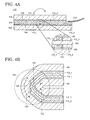
- the first touch electrodes 282 and the second touch electrodes 284 each have a plurality of square regions having a substantially square shape (diamond electrode) and connection regions (not illustrated) connecting the adjacent diamond electrodes.
- the first touch electrodes 282 and the second touch electrodes 284 may exist in the same layer. In this case, over the connection region of one of the first touch electrodes 282 and the second touch electrodes 284 , the connection region of the other (bridge electrode) intersects through an interlayer insulating film (described below).
- the first touch electrodes 282 and the second touch electrodes 284 may exist in different layers with the interlayer insulating film therebetween.
- the polarizing plate has a function to inhibit light incident to the display device 100 from outside and reflected in the display-element layer 200 from being radiated outside from the display device 100 .
- the polarizing plate 290 overlaps with the display region 204 .
- a linear polarizing plate and a circularly polarizing plate may be used as the polarizing plate 290 .
- a circularly polarizing plate is used as the polarizing plate 290 , a stacked structure of a 1 /A plate and a linear polarizing plate may be applied.
- the base film 110 has a function to support the display-element layer 200 , the touch sensor 280 , and the polarizing plate 290 and provide physical strength to the display device 100 .
- the base film 110 may have flexibility.
- the base film 110 may include a polymer material such as a polyimide, a polyamide, a polyester, and a polycarbonate.
- a polymer material with a relatively high glass-transition temperature or melting point such as an aromatic polyimide and an aromatic polyamide (aramide), may be used.
- the cap film 112 has also a function to support the display-element layer 200 and provide physical strength to the display device 100 and protects the display-element layer 200 , the touch sensor 280 , and the polarizing plate 290 in association with the base film 110 . Similar to the base film 110 , the cap film 112 may have flexibility and include a polymer material usable in the base film 110 . Note that, when the pixels 202 , the driver circuits 206 and 208 , and terminals 210 fabricated in the display-element layer 200 are formed over the base film 110 and then the cap film 112 is arranged, a glass-transition temperature or a melting point of the cap film 112 may be lower than that of the base film 110 .
- transmittivity of the base film 110 in a visible region may be lower than that of the cap film 112 , which permits a color of the base film 110 to be deeper than that of the cap film 112 .
- a thickness of the base film 110 and a thickness of the cap film 112 may be independently selected and each may be equal to or more than 3 ⁇ m and equal to or less than 30 ⁇ m, equal to or more than 3 ⁇ m and equal to or less than 15 ⁇ m, or equal to or more than 3 ⁇ m and equal to or less than 10 ⁇ m.
- At least one of the base film 110 and the cap film 112 may be provided with a cut (hereinafter, referred to as a gap or a slit) 120 or 122 as shown in FIG. 1 .
- the gap 120 may pass from a top surface to a bottom surface of the base film 110 .
- the gap 120 separates the base film 110 into two regions.
- the base film 110 has two base films (first base film 110 _ 1 and second base film 110 _ 2 ) separated from each other, and a boundary therebetween corresponds to the gap 120 .
- the boundary is positioned between an edge portion of the first base film 110 _ 1 and an edge portion of the second base film 110 _ 2 .
- the first base film 110 _ 1 and the second base film 110 _ 2 are independent from each other. Therefore, when the first base film 110 includes a polymer material, there is no or substantially no covalent bond between the first base film 110 _ 1 and the second base film 110 _ 2 . However, the first base film 110 _ 1 and the second base film 110 _ 2 may be in physical contact with each other.
- the gap 122 may pass from a top surface to a bottom surface of the cap film 112 ( FIG. 2 ).
- the gap 112 separates the cap film 112 into two regions.
- the cap film 112 has two cap films (first cap film 112 _ 1 and second cap film 112 _ 2 ) separated from each other, and a boundary therebetween corresponds to the gap 122 .
- the boundary is positioned between an edge portion of the first cap film 112 _ 1 and an edge portion of the second cap film 112 _ 2 .
- the first cap film 112 _ 1 and the second cap film 112 _ 2 are independent from each other. Therefore, when the first cap film 112 includes a polymer material, there is no or substantially no covalent bond between the first cap film 112 _ 1 and the second cap film 112 _ 2 . However, the first cap film 112 _ 1 and the second cap film 112 _ 2 may be in physical contact with each other.
- the first protection sheet 102 and the second protection sheet 104 have a function to improve reliability by protecting the display device 100 in addition to a function to provide physical strength to the display device 100 .
- Both or at least one of the first protection sheet 102 and the second protection sheet 104 include a material capable of transmitting visible light. This material may have elasticity, and the first protection sheet 102 and the second protection sheet 104 can include a material which has a high elastic limit and does not readily undergo elastic deformation.
- the first protection sheet 102 and the second protection sheet 104 may have a higher elastic limit than the base film 110 and the cap film 112 .
- a polysiloxane, silicon rubber in which a polysiloxane is cross-linked and the like are represented.
- a polymer such as an acrylonitrile-butadiene-styrene copolymer, a polyurethane, a polybutadiene, a styrene-butadiene copolymer, and a styrene-isoprene copolymer or rubber which is a cross-linked material of these polymers can be used.
- the adhesion layers 106 and 108 are an optional structure and have a function to adhere the first protection sheet 102 and the second protection sheet 104 to the base film 110 and the cap film 112 , respectively.
- a variety of adhesives can be used for the adhesion layers 106 and 108 , and an epoxy-based adhesive, an acryl-based adhesive, an adhesive based on silicon rubber, an olefin-based adhesive, a urethane-based adhesive, and the like may be used.
- the adhesion layers 106 and 108 may be configured to be a pressure-sensitive adhesive.
- the display device 100 can be deformed.
- one or both of the gaps 120 and 122 is/are provided to one or both of the base films 110 and the cap film 112 , by which the display device 100 can be bent or folded by using the gaps 120 and 122 as a center.
- FIG. 3A and FIG. 3B Schematic side views before and after folding the display device 100 are shown in FIG. 3A and FIG. 3B , respectively.
- the first base film 110 _ 1 and the second base film 110 _ 2 overlap with each other ( FIG. 3B ).
- the first cap film 112 _ 1 and the second cap film 112 _ 2 also overlap with each other.
- the edge portion of the first base film 110 _ 1 , the edge portion of the second base film 110 _ 2 , the edge portion of the first cap film 112 _ 1 , and the edge portion of the second cap film 112 _ 2 are bent to form a bent portion 128 .
- the gaps 120 and 122 are located in the bent portion 128 , and the bent portion 128 are sandwiched by flat regions 124 and 126 .
- the polymer materials used in the base film 110 and the cap film 112 are compressed or tensed when applied with an external force, leading to deformation.
- an external force When a magnitude of the external force is equal to or less than an elastic limitation, fracture does not take place. Thus, the strain is released by releasing the force, and the polymer materials return to their original state.
- the external force exceeds the elastic limitation, fracture occurs, and a crack or turbidity is caused in the polymer material.
- the strain remains even if the external force is released, which results in plasticity and inhibits the polymer materials from returning to their original state. Additionally, an attempt to recover the original state results in an adverse influence on the display and causes a decrease in display quality because the shapes of the base film 110 and the cap film 112 irreversibly change due to the residual strain.
- the base film 110 and the cap film 112 has the gap 120 or 122 in the display device 100 . Therefore, the base film 110 or the cap film 112 is separated into a plurality of regions. Although these regions may be in contact with one another, they can independently undergo deformation. Hence, when the display device 100 is folded, the stress generated in the bent portion 128 is not accumulated in the entire base film 110 or the cap film 112 , but dispersed to the separated portions (first base film 110 _ 1 , second base film 110 _ 2 , first cap film 112 _ 1 , and second cap film 112 _ 2 ), thereby preventing the fracture of the base film 110 and the cap film 112 . For example, even when the display device 100 is folded so that a curvature thereof is 1 mm or less, it is possible to prevent fracture of the base film 110 and the cap film 112 .
- the display device 100 further possesses the first protection sheet 102 and the second protection sheet 104 having a higher elastic limit than the base film 110 and the cap film 112 .
- the first protection sheet 102 and the second protection sheet 104 have high durability to bending or folding similar to the base film 110 and the cap film 112 . Therefore, fracture does not take place and the stress does not remain after deformation even when the display device 100 is deformed.
- each layer forming the display-element layer 200 is located at a center of the bent portion 128 . That is, each layer is placed at a vicinity of the middle (center line) between the uppermost surface and the lowest surface of the display device 100 in the bent portion (T 2 is approximately twice T 1 in an enlarged figure of FIG. 3B ). Hence, no stress appears or the stress is small in each layer forming the display-element layer 200 . Additionally, each layer structuring the display-element layer 200 has an extremely small thickness compared with the base film 110 , the cap film 112 , the first protection sheet 102 , and the second protection sheet 104 . Accordingly, influence of the deformation is small and fracture does not readily occur even if the display device 100 is deformed.
- the first protection sheet 102 and the second protection sheet 104 have a higher elastic limit than the base film 110 and the cap film 112 , these protection sheets are not fractured and do not exhibit plasticity while the display device is deformed even if no gap is formed therein. Accordingly, if the display device 100 is repeatedly subjected to folding processes at a small curvature, the display device 100 is not fractured and display quality can be maintained. That is, a display device with high reliability can be produced.
- gaps 120 and 122 there is no limitation to the shape of the gaps 120 and 122 , and an arbitral shape can be employed. Since the cross-sectional shapes of the gaps 120 and 122 are a linear line in the example shown in FIG. 1 to FIG. 3B , side surfaces of the first base film 110 _ 1 and the second base film 110 _ 2 are perpendicular to the top surface and the bottom surface of the base film 110 . Similarly, side surfaces of the first cap film 112 _ 1 and the second cap film 112 _ 2 are also perpendicular to the top surface and the bottom surface of the cap film 112 .
- the gap 120 may have a V-shaped cross-sectional shape.
- the side surface of the first base film 110 _ 1 and the side surface of the second base film 110 _ 2 are inclined from the top surface and the bottom surface of the base film 110 .
- the first base film 110 _ 1 and the second base film 110 _ 2 are spaced from each other at an interface in contact with the adhesion layer 106 (at an interface with the first protection sheet 102 in the case where the adhesive layer 106 is not provided) other than at an interface with the display-element layer 200 .
- the adhesive layer 106 (the interface with the first protection sheet 102 in the case where the adhesive layer 106 is not provided) is able to exist between the side surface of the first base film 110 _ 1 and the side surface of the second base film 110 _ 2 .
- the first protection sheet 102 and the adhesive layer 106 may form a projected portion at a position overlapping with the gap 120 .
- the gap 122 may have a V-shaped cross-sectional shape.
- the side surface of the first cap film 112 _ 1 and the side surface of the second cap film 112 _ 2 are inclined from the top surface and the bottom surface of the cap film 112 .
- the first cap film 112 _ 1 and the second cap film 112 _ 2 are spaced from each other at an interface in contact with the adhesion layer 108 (at an interface with the second protection sheet 104 in the case where the adhesive layer 108 is not provided) other than at an interface with the display-element layer 200 .
- the adhesive layer 108 (the interface with the second protection sheet 104 in the case where the adhesive layer 108 is not provided) is able to exist between the side surface of the first cap film 112 _ 1 and the side surface of the second cap film 112 _ 2 .
- the second protection sheet 104 and the adhesive layer 108 may form a projected portion at a position overlapping with the gap 122 .
- a width of the gap 122 of the cap film 112 is narrowed.
- the first cap film 112 _ 1 and the second cap film 112 _ 2 may make contact with each other, they are not fractured because they are not compressed by each other with a strong force.
- the second protection sheet 104 is compressed by the external force, the protection sheet 104 does not exhibit plasticity and is not fractured even if a compression stress is applied because it has a higher elastic limit than the cap film 112 .
- the cross-sectional shapes of the gap 120 and 122 are not limited to the V-shape and may be a U-shape or another shape. In such a case, at least one of the side surface of the first base film 110 _ 1 , the side surface of the second base film 110 _ 2 , the side surface of the first cap film 112 _ 1 , and the side surface of the second cap film 112 _ 2 has a bent shape.
- a plane layout and the number of the gaps 120 and 122 are also not limited, and they can be designed in view of the place where the display device 100 is bent or folded or the properties (i.e., a position which is readily bent) of the base film 110 and the cap film 112 .
- the base film 110 and the cap film 112 each may have one gap 120 and one gap 122 , respectively.
- these gaps may overlap with each other or may be arranged parallel to each other.
- the gaps 120 and 122 may interest each other.
- the base film 110 and the cap film 112 may each have a plurality of gaps 120 and 122 , respectively.
- the numbers of the gaps 120 and 122 may be different and one of the numbers may be one.
- the gaps 120 and 122 may be arranged so as to extend in a direction parallel to a long side of the display region 204 .
- the display device 100 may have the gaps 120 and 122 parallel to the long side of the display region 204 as well as the gaps 120 and 122 perpendicular thereto.
- the gaps 120 and 122 may be inclined from the long side and the short side of the display region 204 .
- the display device 100 may have a plane layout where each of the gaps 120 and 122 is structured with a plurality of straight lines.
- the display device 100 may have a plane layout where the gaps 120 and 122 each have a curve.
- the gaps 120 and 122 overlap with the display region 204 and may be provided between the display region 204 and the terminals 210 , for example.
- the gaps 120 and 122 overlap with the display region 204 , the gaps 120 and 122 overlap or intersect with a variety of insulating films and wirings in the display-element layer 200 . This mode is explained by using FIG. 6 and FIG. 7 .
- FIG. 6 and FIG. 7 are schematic top views of two adjacent pixels 202 .
- structural elements are illustrated so as not to overlap with one another for visibility. However, the plurality of structural elements may overlap with one another. Additionally, a part of the structural elements is omitted.
- the pixels 202 including a light-emitting element are illustratively demonstrated.
- the display-element layer 200 has wirings including a plurality of gate lines 220 , a plurality of data lines 222 , a plurality of current-supplying lines 224 , and the like.
- the plurality of pixels 202 are electrically connected to the gate line 220 , and two pixels 202 are illustrated in FIG. 6 .
- the data line 222 and the current-supplying line 224 are connected to the plurality of pixels 202 arranged along these wirings.
- the pixel 202 possesses transistors 230 and 250 .
- the transistor 230 has a semiconductor film 232 , a gate 234 , a drain 236 , a source 238 , and the like.
- the gate 234 is a part of the gate line 220
- the drain 236 is a part of the data line 222 .
- the transistor 230 has a so-called double-gate structure having two gates 234 in FIG. 6 . However, the transistor 230 may have one gate or three or more gates.
- the transistor 250 has a part of a semiconductor film 240 , a gate 252 , a drain 254 , a source 256 , and the like.
- the drain 254 is a part of the current-supplying line 224 .
- the source 238 of the transistor 230 is connected to a first capacitor electrode 242 existing in the same layer as the gate line 220 , and a part of the first capacitor electrode 242 functions as the gate 252 of the transistor 250 . Therefore, signals generated by the driver circuit 208 and input from the data line 222 are input to the gate 252 of the transistor 250 through the transistor 230 .
- the semiconductor film 240 and a second capacitor electrode 244 are disposed so as to overlap with the first capacitor electrode 242 .
- an insulating film functioning as a gate insulating film of the transistor 230 and the transistor 250 is provided between the first capacitor electrode 242 and the semiconductor film 240
- an insulating film functioning as an interlayer film covering the gates 234 and 252 of the transistors 230 and the transistor 250 is arranged between the semiconductor film 240 and the second capacitor electrode 244 as described below.
- a capacitor is formed by the first capacitor electrode 242 , the gate insulating film, the semiconductor film 240 , the interlayer film, and the second capacitor electrode 244 and contributes to maintenance of a potential of the gate 252 of the transistor 250 .
- a supplementary capacitor electrode 260 is further provided to the pixel 202 , and the supplementary capacitor electrode 260 may be electrically connected to the current-supplying line 224 .
- a first electrode 270 functioning as a pixel electrode is formed in each pixel 202 .
- the first electrode 270 is not illustrated in the left pixel 202 in FIG. 6 for visibility.
- the first electrode 270 is electrically connected to the source 256 of the transistor 250 .
- a supplementary capacitor is formed by the supplementary capacitor electrode 260 , the first electrode 270 , and an insulating film provided therebetween and contributes to maintenance of the potential of the gate 252 of the transistor 250 .
- a second electrode 278 is formed over the first electrode 270 .
- the second electrode 278 is provided over the plurality of pixels 202 . Therefore, the second electrode 278 is shared by the plurality of pixels 202 .
- An EL layer not illustrated is formed between the first electrode 270 and the second electrode 278 , by which the light-emitting element 268 is formed.
- the pixel 202 may further possess another element such as a transistor and a capacitor and a wring.
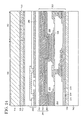
- gaps 120 and 122 are formed by dotted lines in FIG. 6 and FIG. 7 .
- the gaps 120 and 122 are formed in the base film 110 and the cap film 122 , respectively, and separate the base film 110 and the cap film 112 to give the plurality of regions.
- the gaps 120 and 122 perpendicular to the gate line 220 respectively separate the base film 110 and the cap film 112 into a first region 150 and a second region 152 .
- the gate line 220 , the first electrode 270 , and the second electrode 278 extend over the first region 150 and the second region 152 and overlap or intersect with the gaps 120 and 122 .
- the gaps 120 and 122 parallel to the gate line 220 respectively separate the base film 110 and the cap film 112 into a third region 154 and a forth region 156 .
- the data line 222 , the current-supplying line 224 , the first electrode 270 , the second electrode 278 , the supplementary capacitor electrode 260 , and the like extend over the third region 154 and the fourth region 156 and overlap or intersect with the gaps 120 and 122 .
- the first region 150 and the second region 152 respectively correspond to the first base film 110 _ 1 and the second base film 110 _ 2 (alternatively, the first cap film 112 _ 1 and the second cap film 112 _ 2 ). Therefore, the gate line 220 , the first electrode 270 , and the second electrode 278 extend over the first base film 110 _ 1 and the second base film 110 _ 2 (the first cap film 112 _ 1 and the second cap film 112 _ 2 ) and intersect or overlap with a boundary between the first base film 112 _ 1 and the second base film 110 _ 2 (between the first cap film 112 _ 1 and the second cap film 112 _ 2 ).
- the third region 154 and the fourth region 156 respectively correspond to the first base film 110 _ 1 and the second base film 110 _ 2 (alternatively, the first cap film 112 _ 1 and the second cap film 112 _ 2 ).
- the data line 222 , the current-supplying line 224 , the first electrode 270 , the second electrode 278 , the supplementary capacitor electrode 260 , and the like extend over the first base film 110 _ 1 and the second base film 110 _ 2 (the first cap film 112 _ 1 and the second cap film 112 _ 2 ) and overlap or intersect with a boundary between the first base film 110 _ 1 and the second base film 110 _ 2 (between the first cap film 112 _ 1 and the second cap film 112 _ 2 ).
- both or at least one of the base film 110 and the cap film 112 are/is provided with the gaps 120 and 122 , which improves durability of the display device 100 to deformation. Accordingly, a display device with high reliability can be produced.
- FIG. 8 An example of a process flow of the display device 100 is schematically shown in FIG. 8 .
- the base film 110 is formed over a first supporting substrate 140 (S 1 ). After that, the display-element layer 200 is formed over the base film 110 (S 2 ).
- the cap film 112 is formed over another second supporting substrate 142 (S 1 ), over which the polarizing plate 290 and the touch sensor 280 are successively formed (S 2 ).
- the first supporting substrate 140 and the second supporting substrate 142 are bonded to each other so that the base film 110 , the display-element layer 200 , the polarizing plate 290 , the touch sensor 280 , and the cap film 112 are sandwiched therebetween (S 3 ).
- the second supporting substrate 142 is separated from the cap film 112 , which is followed by formation of the gap 122 by irradiating the cap film 112 with light such as a laser or mechanical formation of the gap 122 by using a knife or the like (S 4 and S 5 ).
- the second protection sheet 104 is bonded to the cap film 112 via the adhesion layer 108 (S 5 ). After that, the first supporting substrate 140 is separated from the base film 110 (S 6 ), and the gap 120 is formed in the base film 110 with the same method as that of the gap 122 (S 6 and S 7 ).
- the first protection sheet 102 is bonded to the base film 110 via the adhesion layer 106 (S 8 ).
- the display device 100 can be manufactured.
- the gap 120 is formed in the base film 110 after the formation of the gap 122 in the cap film 112 .
- the order is not limited.
- the first supporting substrate 140 may be first separated after bonding the first supporting substrate 140 and the second supporting substrate 142 .
- the gap 120 may be formed in the base film 110 , and then the bonding of the first protection sheet 102 , the separation of the second supporting substrate 142 , and the formation of the gap 122 in the cap film 112 may be sequentially performed.
- the display device 100 may also be prepared with a flow (process flow 2 ) shown in FIG. 9 .
- the process flow shown in FIG. 9 is different from the process flow 1 in that the adhesion layers 106 and 108 are not used when the first protection sheet 102 and the second protection sheet 104 are bonded (S 5 , S 8 ). In this case, the first protection sheet 102 and the second protection sheet 104 are in direct contact with the base film 110 and the cap film 112 , respectively.
- the display device 100 may be manufactured by using the adhesion layer in bonding one of the protection sheet 102 and the second protection sheet 104 without the use of any adhesion layer when the other is bonded.
- the display device 100 may also be prepared with a flow (process flow 3 ) shown in FIG. 10 .
- the process flow shown in FIG. 10 is different from the process flow 1 in that the polarizing plate 290 is formed after the touch sensor 280 is formed over the second supporting substrate 142 (S 2 ).
- the use of this flow allows a distance between the touch sensor 280 and the second electrode 278 of the light-emitting element 268 to be increased. Hence, influence of an electric field by the second electrode 278 of the light-emitting element 268 on the operation of the touch sensor 280 can be reduced, by which a touch can be sensed with higher sensitivity at higher accuracy.
- the display device 100 may also be prepared with a flow (process flow 4 ) shown in FIG. 11 .
- the process flow shown in FIG. 11 is different from the process flow 1 in that the touch sensor 280 is formed over the display-element layer 200 after the display-element layer 200 is formed over the first substrate 140 (S 2 ).
- the use of this flow allows direct formation of the touch sensor 280 over a variety of elements such as the transistors 230 and 250 , the capacitors, and the light-emitting element 268 , by which the wirings for driving the touch sensor 280 as well as the wirings for driving the pixels 202 and the terminals 210 of the display-element layer 200 can be integrated in the same layer.
- the signals can be supplied to the display-element layer 200 and the touch sensor 280 by using one connector 212 .
- the display device 100 may also be prepared with a flow (process flow 5 ) shown in FIG. 12 .
- the process flow shown in FIG. 12 is different from the process flow 1 in that the gaps 120 and 122 are prepared by performing light irradiation or mechanical processing on the base film 110 and the cap film 112 after the base film 110 and the cap film 112 are respectively formed over the first supporting substrate 140 and the second supporting substrate 142 (S 1 ) and before the display-element layer 200 , the polarizing plate 290 , and the touch sensor 280 are formed. (S 2 ).
- FIG. 13A to FIG. 26 correspond to a cross section of a region extending through the plurality of pixels 202 .
- FIG. 13A to FIG. 26 may not be consistent with the layout of the pixels 202 shown in FIG. 6 and FIG. 7 , the elements indicated by the same reference number are the same in each figure.
- the base film 110 is first formed over the first supporting substrate 140 .
- the first supporting film 140 has a function to support the base film 110 , the display-element layer 200 , the touch sensor 280 , the polarizing plate 290 , and the like. Therefore, a material having heat resistance to the process temperature of these structural members formed thereover and chemical stability to the chemicals used in the process can be used for the first supporting substrate 140 .
- the first supporting substrate 140 may include glass, quartz, plastics, a metal, ceramics, and the like.
- the base film 110 is an insulating film with flexibility and may include a material selected from the polymer materials described in the First Embodiment.
- the base film 110 can be formed by applying a wet-type film-forming method such as a printing method, an ink-jet method, a spin-coating method, and a dip-coating method or a lamination method.
- the undercoat 214 is a film having a function to prevent impurities such as an alkaline metal from diffusing to the display-element layer 200 from the first supporting substrate 140 and the base film 110 and may include an inorganic insulator such as silicon nitride, silicon oxide, silicon nitride oxide, and silicon oxynitride.
- the undercoat 214 can be formed to have a single-layer or stacked-layer structure by applying a chemical vapor deposition method (CVD method), a sputtering method, or the like.
- a structure can be used where a film including silicon nitride is sandwiched by films including silicon oxide.
- the undercoat 214 may not be provided or may be formed to cover a part of the base film 110 .
- the semiconductor film 240 may contain Group 14 elements such as silicon, for example. Crystallinity of the semiconductor film 240 is not limited, and the semiconductor film 240 may exist in a crystal state of a single crystalline, polycrystalline, microcrystalline, or amorphous state. Alternatively, these crystalline states may be mixed in the semiconductor film 240 . Alternatively, the semiconductor film 240 may include an oxide semiconductor. As an oxide semiconductor, Group 13 elements such as indium and gallium are represented, and a mixed oxide of indium and gallium (IGO) is exemplified. When an oxide semiconductor is used, the semiconductor film 240 may further contain a Group 12 element, and a mixed oxide of indium, gallium, and zinc (IGZO) is given as an example.
- Group 14 elements such as silicon, for example. Crystallinity of the semiconductor film 240 is not limited, and the semiconductor film 240 may exist in a crystal state of a single crystalline, polycrystalline, microcrystalline, or amorphous state. Alternatively, these crystalline states may be mixed in the semiconductor
- the semiconductor film 240 may be prepared with a CVD method by using silane gas and the like as a raw material. A heat treatment or application of light such as a laser may be performed on amorphous silicon obtained to conduct crystallization.
- the semiconductor film 240 includes an oxide semiconductor, the semiconductor film 240 can be formed by utilizing a sputtering method or the like.
- a first doping is conducted on the semiconductor film 240 to form doped regions 240 _ 2 and an undoped region 240 _ 1 ( FIG. 13C ).
- a resist film is formed over a portion where the undoped regions 240 _ 1 are to be formed, and then the semiconductor film 240 is doped with ions. Ions of phosphorus and nitrogen imparting a n-type conductivity may be used. After that, the resist film is removed to obtain the state shown in FIG. 13C .
- the gate insulating film 216 is prepared so as to cover the semiconductor film 240 ( FIG. 14A ).
- the gate insulating film 216 may have a single-layer structure or a stacked-layer structure and may include a material usable for the undercoat 214 .
- the gate insulating film 216 can be prepared with a CVD method, or a sputtering method, or the like.
- the gate 252 and the first capacitor electrode 242 existing in the same layer as the gate 252 are formed over the gate insulating film 216 with a sputtering method or a CVD method ( FIG. 14A ).
- the gate electrode 252 is provided so as to overlap with the undoped region 240 _ 1 .
- the gate 252 may be formed with a metal such as titanium, aluminum, copper, molybdenum, tungsten, and tantalum or an alloy thereof so as to have a single-layer or stacked-layer structure.
- a structure in which a highly conductive metal such as aluminum and copper is sandwiched by a metal with a relatively high melting point, such as titanium, tungsten, and molybdenum can be employed.
- a second doping is carried out on the semiconductor film 240 by using the gate 252 as a mask ( FIG. 14B ).
- the doping conditions at this time are adjusted so that the semiconductor film 240 is doped at a lower concentration compared with that of the first doping.
- low-concentration doped regions 240 _ 3 are formed in the regions of the undoped region 240 _ 1 which do not overlap with the gate 252 over the undoped region 240 _ 1 .
- the low-concentration doped regions 240 _ 3 have a lower impurity concentration than the doped regions 240 _ 2 .
- the undoped region 240 _ 1 is a region undoped or substantially undoped with impurities and functions as a channel region.
- the interlayer film 218 is formed over the first capacitor electrode 242 ( FIG. 14C ).
- the interlayer film 218 may have a single-layer or stacked layer structure, may include a material usable for the undercoat 214 , and may be prepared with a CVD method, a sputtering method, or the like.
- etching is performed on the interlayer film 218 and the gate insulating film 216 to form opening portions reaching the doped regions 240 _ 2 ( FIG. 15A ).
- the opening portions can be prepared, for example, by conducting plasma etching in a gas including a fluorine-containing hydrocarbon.
- a metal film is formed to cover the opening portions and processed with etching to form a source 256 and a drain 254 ( FIG. 15B ).
- the transistor 250 is fabricated.
- the source 256 also serves as the second capacitor electrode 244 and partly overlaps with the first capacitor electrode 242 .
- the capacitor 246 is formed by the doped region 240 _ 2 and the gate insulating film 216 which overlap with the first capacitor electrode 242 , the first capacitor electrode 242 , the interlayer film 218 sandwiched by the first capacitor electrode 242 and the second capacitor electrode 244 , and the second capacitor electrode 244 .
- the capacitor 246 contributes to maintenance of a potential of the gate 252 .
- the metal film may include a metal usable for the gate 252 and may have a single-layer or stacked layer structure.
- the metal film can be formed by applying a sputtering method or a CVD method.
- the leveling film 226 has a function to absorb depressions and projections caused by the transistor 250 , the capacitor 246 , and the like and provide a flat surface.
- the leveling film 226 can be prepared with an organic insulator.
- an organic insulator a polymer material such as an epoxy resin, an acrylic resin, a polyimide, a polyamide, a polyester, a polycarbonate, and a polysiloxane is represented, and the leveling film 226 can be formed with the aforementioned wet-type film-forming method.
- the leveling film 226 may have a stacked-layer structure of a layer including the aforementioned organic insulator and a layer including an inorganic insulator.
- a silicon-containing inorganic insulator such as silicon oxide, silicon nitride, silicon nitride oxide, and silicon oxynitride is represented as an inorganic insulator, and a film including these materials can be formed with a sputtering method or a CVD method.
- connection electrode 248 is prepared so as to cover this opening portion ( FIG. 16A ).
- the connection electrode 248 may be formed by using a conductive oxide transmitting visible light, such as indium-tin oxide (ITO) and indium-zinc oxide (IZO), with a sputtering method or the like. Note that it is not always necessary to form the connection electrode 248 .
- the formation of the connection electrode 248 enables protection of an exposed metal surface such as a surface of the source 256 in the following processes, by which an increase in contact resistance can be prevented.
- the supplementary capacitor electrode 260 is formed by using a metal such as aluminum, copper, titanium, molybdenum, tungsten, and tantalum or an alloy thereof ( FIG. 16B ).
- the supplementary capacitor electrode 260 may also have a single layer structure or a stacked layer structure, and a stacked-layer structure of molybdenum/aluminum/molybdenum may be employed, for example.
- the supplementary capacitor electrode 260 forms the supplementary capacitor 262 in association with the first electrode 270 of the light-emitting element 268 formed later.
- the insulating film 228 is formed ( FIG. 16B ).
- the insulating film 228 may include a material usable for the undercoat 214 and the gate insulating film 216 , such as silicon nitride, and the formation method thereof can be applied.
- the insulating film 228 has an opening portion for exposing a contact portion (that is, a bottom surface of the connection electrode 248 formed in the opening portion formed in the leveling film 226 ) where an electrical connection between the transistor 250 and the light-emitting element 268 is conducted.
- the first electrode 270 of the light-emitting element 268 is formed ( FIG. 17A ).
- a material having a light-transmitting property exemplified by a conductive oxide such as ITO and IZO can be used.
- a metal such as aluminum and silver or an alloy thereof may be used.
- stacked layers of the metal or alloy with the conductive oxide such as a stacked-layer structure in which the metal is sandwiched by the conductive oxide (e.g., ITO/silver/ITO), can be employed.
- the supplementary capacitor 262 is formed by the first electrode 270 , the supplementary capacitor electrode 260 , and the insulating film 228 sandwiched therebetween.
- a partition wall 229 is formed ( FIG. 17A ).
- the partition wall 229 has a function to absorb steps caused by an edge portion of the first electrode 270 and the opening portion provided in the leveling film 226 and electrically insulate the first electrodes 270 of the adjacent pixels 202 .
- the partition wall 229 is also called a bank (rib).
- the partition wall 229 may be prepared with a material usable for the leveling film 226 .
- the partition wall 229 has an opening exposing a part of the first electrode 270 , and an edge of the opening portion is preferred to have a gradually tapered shape. When the edge of the opening portion has a steep slope with respect to the first electrode 270 , coverage failure of the EL layer 274 and the second electrode 278 formed later readily occurs.
- an opening portion 258 may be provided to the insulating film 228 so that the leveling film 226 and the partition wall 229 make direct contact with each other.
- the use of such a structure allows impurities such as water eliminated from the leveling film 226 to be released in the heat treatment and the like after the formation of the partition wall 229 .
- the EL layer 274 of the light-emitting element 268 and the second electrode 274 over the EL layer 274 are formed ( FIG. 17B ).
- a structure is illustrated in which the EL layer 274 is composed of a first layer 274 _ 1 , a second layer 274 _ 2 , and a third layer 274 _ 3 .
- the present embodiment is not limited thereto, and an EL layer having a single-layer structure or an EL layer having a structure of four or more layers may be employed.
- a carrier-injection layer, a carrier-transporting layer, an emission layer, a carrier-blocking layer, an exciton-blocking layer, and the like may be appropriately used.
- one layer may have a plurality of functions.
- the EL layer 274 can be prepared with an evaporation method, an ink-jet method, a printing method, a spin-coating method, or the like.
- the first layer 274 _ 1 and the third layer 274 _ 3 of the EL layer 274 are a carrier-injection layer, a carrier-transporting layer, or stacked layers thereof and are formed so as to extend over the adjacent pixels 202 . That is, they are shared by each of the pixels 202 .
- the second layer 274 _ 2 is an emission layer and may have a different material or structure in every pixel 202 . Thus, emission colors different between the adjacent pixels 202 can be obtained, thereby enabling a full-color display.
- the second layer 274 _ 2 may be configured to be white emissive and shared by all of the pixels 202 . In this case, a wavelength of light extracted from each pixel 202 is selected by using a color filter or the like to perform a full-color display.
- the second electrode 278 is formed.
- the light-emitting element 268 is fabricated by the first electrode 270 , the EL layer 274 , and the second electrode 278 .
- Carriers (electrons and holes) are injected to the EL layer 274 from the first electrode 270 and the second electrode 278 , and recombination of the carriers results in an excited state.
- Light-emission is obtained through a relaxation process of the excited state to a ground state.
- a region in which the EL layer 274 and the first electrode 270 are in direct contact with each other is an emission region in the light-emitting element 268 .
- a metal such as aluminum and silver or an alloy thereof can be used for the second electrode 278 .
- the second electrode 278 is prepared by using the metal or the alloy so as to have a thickness to transmit visible light.
- a material having a light-transmitting property such as a conductive oxide exemplified by ITO and IZO, can be used for the second electrode 278 .
- a stacked-layer structure of the metal or alloy with the conductive oxide e.g., M-Ag/ITO, etc. may be employed for the second electrode 278 .
- a protection film (passivation film) 292 is formed as an optional structure ( FIG. 18 ).
- the passivation film 292 has a function to prevent moisture from entering the light-emitting element 268 from outside and is preferred to have a high gas-barrier property.
- the structure of the passivation film 292 can be arbitrarily determined and may have a three-layer (a first layer 294 , a second layer 296 , and a third layer 298 ) structure as shown in FIG. 18 .
- the first layer 294 may include an inorganic material such as silicon nitride, silicon oxide, silicon nitride oxide, and silicon oxynitride and can be formed with a CVD method or a sputtering method, for example.
- the second layer 296 is formed ( FIG. 18 ).
- the second layer 296 may include an organic resin including an acrylic resin, a polysiloxane, a polyimide, and a polyester. Furthermore, as shown in FIG. 18 , the second layer 296 may be formed at a thickness so that depressions and projections caused by the partition wall 229 are absorbed and a flat surface is provided.
- the second layer 296 may be formed by a wet-type film-forming method such as an ink-jet method.
- the second layer 296 may be prepared by atomizing or vaporizing oligomers serving as a raw material of the aforementioned polymer material at a reduced pressure, spraying the first layer 294 with the oligomers, and then polymerizing the oligomers.
- the third layer 298 may include a material usable in the first layer 294 and may be formed with the method applicable to the formation of the first layer 294 .
- the display-element layer 200 is fabricated.
- the touch sensor 280 is formed as an optional structure.
- an insulating film 286 is formed over the passivation film 292 ( FIG. 19 ).
- the insulating film 286 has a function to increase a distance between the light-emitting element 268 and the touch sensor 280 or a function to adhere the first touch electrode 282 or the second touch electrode 284 of the touch sensor 280 to the display-element layer 200 .
- the insulating film 286 may contain a silicon-containing inorganic compound such as silicon oxide, silicon nitride, silicon oxynitride, and silicon nitride oxide or a polymer material such as an epoxy resin, an acrylic resin, a polyimide, a polyamide, a polyester, and a polycarbonate.
- the insulating film 286 can be formed by applying a CVD method or a sputtering method. When a polymer material is used, a wet-type film-forming method or a lamination method may be used. Note that the insulating film 286 is an optional structure and may not be provided.
- the first touch electrode 282 and the second touch electrode 284 are formed ( FIG. 19 ).
- the first touch electrode 282 and the second touch electrode 284 may include a transparent conductive oxide such as ITO and IZO and can be formed with a sputtering method.
- the first touch electrode 282 and the second touch electrode 284 may be prepared in a mesh form in a plane view so as to be disposed in a region which does not overlap with the light-emitting element. In this case, since a light-transmitting property is not required, a metal material with low resistance can be used.
- a mode is illustrated where the first touch electrode 282 and the second touch electrode 284 exist in the same layer. In this case, the first touch electrode 282 and the second touch electrode 284 can be prepared at the same time.
- the interlayer insulating film 289 is formed over the first touch electrode 282 and the second touch electrode 284 ( FIG. 20 ).
- the interlayer insulating film 289 may include a material usable in the insulating film 286 and may be formed with a method applicable to the formation of the insulating film 286 .
- the bridge electrode 288 connecting the diamond electrodes of the second touch electrode 284 is formed.
- the bridge electrode 288 may also include a transparent conductive oxide and can be formed by using a sputtering method.
- the touch sensor 280 is fabricated.
- a protection film for protecting the touch sensor 280 may be disposed over the touch sensor 280 .
- the protection film may include a polymer material such as a polyester, an epoxy resin, and an acrylic resin and can be formed by applying a wet-type film-forming method or a lamination method.
- the cap film 112 is formed over the second supporting substrate 142 .
- a substrate including a material usable for the first supporting substrate 140 can be used.
- the cap film 112 can be formed with a material usable in the base film 110 .
- the glass transition temperature or the melting point of the cap film 112 may be lower than that of the base film 110 .
- the transmittivity of the base film 110 in a visible region may be lower than that of the cap film 112 .
- the base film 110 may have a deeper color than the cap film 112 .
- the polarizing plate 290 is formed over the cap film 112 ( FIG. 21B ).
- the polarizing plate 290 may be a linear polarizing plate or a circularly polarizing plate. It is preferred to use a circularly polarizing plate in order to effectively suppress reflection of external light in the display-element layer 200 .
- the first supporting substrate 140 and the second supporting substrate 142 are bonded with an adhesion layer 300 so as to sandwich the display-element layer 200 , the touch sensor 280 , and the polarizing plate 290 .
- An adhesive arbitrarily selected from an epoxy-based adhesive, an acrylic-based adhesive, an adhesive based on silicon rubber, an olefin-based adhesive, a urethane-based adhesive, and the like can be used for the adhesion layer 300 .
- the second supporting substrate 142 is peeled off. Specifically, light such as laser light is applied from a side of the second supporting substrate 142 to reduce the adhesion between the second supporting substrate 142 and the cap film 112 . Then, the cap film 112 is separated from the second supporting substrate 142 using physical force ( FIG. 23 ).
- a solid laser such as a ruby laser, an yttrium-aluminum-garnet (YAG) laser, a titanium-sapphire laser, and a semiconductor laser
- a liquid laser such as a pigment laser
- a gas laser such as a helium-neon laser, an argon-ion laser, a carbon-dioxide laser, a nitrogen laser, an excimer laser, a metal-vapor laser, and a helium-cadmium laser, and the like can be used.
- a laser may be selected which has an oscillation wavelength in an absorption wavelength of the cap film 112 .
- the formation of the gap 122 may be carried out by physically removing a part of the cap film 112 with a knife or the like.
- the gap 122 is formed so as to pass from the top surface to the bottom surface of the cap film 112 .
- the gap 122 may be provided to overlap with the variety of insulating films in the display-element layer 200 .
- the gap 122 can be arranged so as to overlap with the insulating films such as the undercoat 214 , the gate insulating film 216 , the interlayer film 218 , the leveling film 226 , the insulating film 222 forming the supplementary capacitor 262 , the partition wall 229 , the EL layer 274 , and each of the layers included in the passivation film 292 .
- the gap 122 may be formed so as to overlap with the emission region of the light-emitting element 268 .
- the aforementioned insulating films are also prepared outside the display region 204 .
- the insulating films are formed between the display region 204 and the terminals 210 . Therefore, as shown in FIG. 5D , these insulating films are able to overlap with the gap 122 when the gap 122 is formed between the display region 204 and the terminals 210 .
- the gap 122 separates the cap film 112 into the plurality of regions.
- the gap 122 separates the cap film 112 into the first region 150 and the second region 152 .
- the aforementioned insulating films extend over the first region 150 and the second region 152 and overlap with the gap 122 .
- the gap 122 separates the cap film 112 to provide the first cap film 112 _ 1 and the second cap film 112 _ 2 which correspond to the first region 150 and the second region 152 , respectively. Therefore, the aforementioned insulating films extend over the first cap film 112 _ 1 and the second cap film 112 _ 2 and overlap with the boundary between the first cap film 112 _ 1 and the second cap film 112 _ 2 .
- the second protection sheet 104 is bonded to the cap film 112 by using the adhesion layer 108 .
- the adhesion layer 108 and the second protection sheet 104 those described in the First Embodiment can be used.
- a polymer usable for the second protection sheet 104 (see the First Embodiment) or a solution or a dispersion of a precursor or an oligomer thereof is applied over the cap film 112 , and then a solvent is evaporated.
- a polymer the polymer may be cross-linked after being applied onto the cap film.
- a polymer reaction may be conducted after evaporating a solvent.
- an oligomer is used, polymerization may be carried out after evaporating a solvent.
- the gap 120 is formed in the base film 110 .
- the second supporting substrate 142 shown in FIG. 24 is separated from the base film 110 . This separation may be performed in a similar manner as that of the first supporting substrate 140 from the cap film 112 .
- the gap 120 is formed by performing light irradiation or physical disconnection on the base film 110 ( FIG. 25 ).
- the gap 120 may be provided so as to overlap with the variety of insulating films in the display-element layer 200 .
- the gap 120 may be formed so as to overlap with the insulating films such as the undercoat 214 , the gate insulating film 216 , the interlayer film 218 , the leveling film 226 , the insulating film 222 forming the supplementary capacitor 262 , the partition wall 229 , the EL layer 274 , and each of the layers included in the passivation film 292 .
- the gap 120 may be formed so as to overlap with the emission region of the light-emitting element.
- the gap 120 separates the base film 110 into the plurality of regions.
- the gap 120 separates the base film 110 into the first region 150 and the second region 152 .
- the aforementioned insulating films extend over the first region 150 and the second region 152 and overlap with the gap 120 .
- the gap 120 separates the base film 110 to provide the first base film 110 _ 1 and the second base film 112 _ 2 which correspond to the first region 150 and the second region 152 , respectively. Therefore, the aforementioned insulating films extend over the first base film 102 _ 1 and the second base film 102 _ 2 and overlap with the boundary between the first base film 110 _ 1 and the second base film 110 _ 2 .
- these insulating films may overlap with the gap 120 when the gap 120 is formed between the display region 204 and the terminals 210 .
- the first protection sheet 102 is bonded to the base film 110 with the adhesion layer 106 .
- the adhesion layer 106 and the first protection sheet 102 those described in the First Embodiment can be used.
- the first protection sheet 102 can be prepared with the same method as that of the protection sheet 104 .
- the display device 100 can be manufactured. As described in the First Embodiment, both or one of the base film 110 and the cap film 112 are/is provided with the gaps 120 and/or 122 , and the first protection sheet 102 and the second protection sheet 104 sandwiching the display-element layer 200 , the base film 110 , and the cap film 112 have higher elastic limits than the base film 110 and the cap film 112 . Therefore, the base film 110 , the cap film 112 , the first protection sheet 102 , and the second protection sheet 104 are not fractured even if the display device 100 is folded at a small curvature, and a flexible display device with high reliability can be produced.
- the embodiments can be applied to any kind of display devices of the flat panel type such as other self-emission type display devices, liquid crystal display devices, and electronic paper type display device having electrophoretic elements and the like.
- the size of the display device is not limited, and the embodiment can be applied to display devices having any size from medium to large.
Landscapes
- Engineering & Computer Science (AREA)
- Manufacturing & Machinery (AREA)
- Devices For Indicating Variable Information By Combining Individual Elements (AREA)
- Microelectronics & Electronic Packaging (AREA)
- Physics & Mathematics (AREA)
- Optics & Photonics (AREA)
- Electroluminescent Light Sources (AREA)
Abstract
Description
Claims (17)
Applications Claiming Priority (2)
| Application Number | Priority Date | Filing Date | Title |
|---|---|---|---|
| JP2016203210A JP2018066769A (en) | 2016-10-17 | 2016-10-17 | Display device |
| JP2016-203210 | 2016-10-17 |
Publications (2)
| Publication Number | Publication Date |
|---|---|
| US20180108851A1 US20180108851A1 (en) | 2018-04-19 |
| US10340468B2 true US10340468B2 (en) | 2019-07-02 |
Family
ID=61904744
Family Applications (1)
| Application Number | Title | Priority Date | Filing Date |
|---|---|---|---|
| US15/698,739 Active US10340468B2 (en) | 2016-10-17 | 2017-09-08 | Display device |
Country Status (2)
| Country | Link |
|---|---|
| US (1) | US10340468B2 (en) |
| JP (1) | JP2018066769A (en) |
Families Citing this family (7)
| Publication number | Priority date | Publication date | Assignee | Title |
|---|---|---|---|---|
| JP6826881B2 (en) * | 2016-12-22 | 2021-02-10 | 株式会社ジャパンディスプレイ | Protective member, display device and manufacturing method of display device |
| KR102441930B1 (en) * | 2017-12-04 | 2022-09-14 | 삼성디스플레이 주식회사 | Flexible display device and method for manufacturing the flexilbe display device |
| US10916717B2 (en) * | 2018-05-29 | 2021-02-09 | Wuhan China Star Optoelectronics Semiconductor Display Technology Co., Ltd. | Flexible organic light emitting diode display assembly |
| JP6609351B1 (en) * | 2018-06-18 | 2019-11-20 | デクセリアルズ株式会社 | Polarizing plate and manufacturing method thereof |
| WO2020065910A1 (en) * | 2018-09-28 | 2020-04-02 | シャープ株式会社 | Method for manufacturing display device |
| CN209912874U (en) * | 2019-08-05 | 2020-01-07 | 北京京东方技术开发有限公司 | Display substrate, display device |
| JP7204611B2 (en) * | 2019-08-05 | 2023-01-16 | デクセリアルズ株式会社 | Polarizing plate and manufacturing method thereof |
Citations (2)
| Publication number | Priority date | Publication date | Assignee | Title |
|---|---|---|---|---|
| JP2015026055A (en) | 2013-07-29 | 2015-02-05 | 三星ディスプレイ株式會社Samsung Display Co.,Ltd. | Foldable display device |
| US20160181346A1 (en) * | 2014-12-23 | 2016-06-23 | Lg Display Co., Ltd. | Flexible Display Device with Gate-In-Panel Circuit |
-
2016
- 2016-10-17 JP JP2016203210A patent/JP2018066769A/en active Pending
-
2017
- 2017-09-08 US US15/698,739 patent/US10340468B2/en active Active
Patent Citations (3)
| Publication number | Priority date | Publication date | Assignee | Title |
|---|---|---|---|---|
| JP2015026055A (en) | 2013-07-29 | 2015-02-05 | 三星ディスプレイ株式會社Samsung Display Co.,Ltd. | Foldable display device |
| US9639121B2 (en) | 2013-07-29 | 2017-05-02 | Samsung Display Co., Ltd. | Foldable display |
| US20160181346A1 (en) * | 2014-12-23 | 2016-06-23 | Lg Display Co., Ltd. | Flexible Display Device with Gate-In-Panel Circuit |
Also Published As
| Publication number | Publication date |
|---|---|
| US20180108851A1 (en) | 2018-04-19 |
| JP2018066769A (en) | 2018-04-26 |
Similar Documents
| Publication | Publication Date | Title |
|---|---|---|
| US10340468B2 (en) | Display device | |
| US10353501B2 (en) | Display device | |
| US10809553B2 (en) | Flexible substrate | |
| US10217956B2 (en) | Display device | |
| US10153322B2 (en) | Organic light emitting display device | |
| US9899428B2 (en) | Display device having terminal electrode including stepped surface | |
| US9524992B2 (en) | Thin film transistor array panel and manufacturing method thereof | |
| US20120262660A1 (en) | Display device | |
| KR101320787B1 (en) | Substrate and process for production thereof, and display device | |
| US20180113546A1 (en) | Display device and manufacturing method thereof | |
| US10290821B2 (en) | Display device and manufacturing method of the same | |
| US11644702B2 (en) | Semiconductor substrate | |
| US10061419B2 (en) | Display device | |
| WO2018193681A1 (en) | Display device and method for manufacturing display device | |
| US9035298B2 (en) | Semiconductor device, TFT substrate, and method for manufacturing semiconductor device and TFT substrate | |
| CN107564934A (en) | Display device and preparation method thereof | |
| JP2018081532A (en) | Touch sensor and display device | |
| US20070031642A1 (en) | Adhesive tape for a flexible display device and method of manufacturing a flexible display device using the same | |
| US20240414961A1 (en) | Display apparatus | |
| JP2019102526A (en) | Display device, and method for manufacturing the display device |
Legal Events
| Date | Code | Title | Description |
|---|---|---|---|
| AS | Assignment |
Owner name: JAPAN DISPLAY INC., JAPAN Free format text: ASSIGNMENT OF ASSIGNORS INTEREST;ASSIGNOR:CHENG, HSIANG-YUAN;REEL/FRAME:043793/0980 Effective date: 20140801 |
|
| FEPP | Fee payment procedure |
Free format text: ENTITY STATUS SET TO UNDISCOUNTED (ORIGINAL EVENT CODE: BIG.); ENTITY STATUS OF PATENT OWNER: LARGE ENTITY |
|
| STPP | Information on status: patent application and granting procedure in general |
Free format text: NOTICE OF ALLOWANCE MAILED -- APPLICATION RECEIVED IN OFFICE OF PUBLICATIONS |
|
| STPP | Information on status: patent application and granting procedure in general |
Free format text: PUBLICATIONS -- ISSUE FEE PAYMENT VERIFIED |
|
| STCF | Information on status: patent grant |
Free format text: PATENTED CASE |
|
| MAFP | Maintenance fee payment |
Free format text: PAYMENT OF MAINTENANCE FEE, 4TH YEAR, LARGE ENTITY (ORIGINAL EVENT CODE: M1551); ENTITY STATUS OF PATENT OWNER: LARGE ENTITY Year of fee payment: 4 |
|
| AS | Assignment |
Owner name: MAGNOLIA WHITE CORPORATION, JAPAN Free format text: ASSIGNMENT OF ASSIGNORS INTEREST;ASSIGNOR:JAPAN DISPLAY INC.;REEL/FRAME:072130/0313 Effective date: 20250625 |