US10305447B2 - Acoustic wave filter with enhanced rejection - Google Patents
Acoustic wave filter with enhanced rejection Download PDFInfo
- Publication number
- US10305447B2 US10305447B2 US15/443,740 US201715443740A US10305447B2 US 10305447 B2 US10305447 B2 US 10305447B2 US 201715443740 A US201715443740 A US 201715443740A US 10305447 B2 US10305447 B2 US 10305447B2
- Authority
- US
- United States
- Prior art keywords
- capacitive
- acoustic
- interdigitated
- fingers
- filter
- Prior art date
- Legal status (The legal status is an assumption and is not a legal conclusion. Google has not performed a legal analysis and makes no representation as to the accuracy of the status listed.)
- Active, expires
Links
Images


Classifications
-
- H—ELECTRICITY
- H03—ELECTRONIC CIRCUITRY
- H03H—IMPEDANCE NETWORKS, e.g. RESONANT CIRCUITS; RESONATORS
- H03H9/00—Networks comprising electromechanical or electro-acoustic elements; Electromechanical resonators
- H03H9/46—Filters
- H03H9/64—Filters using surface acoustic waves
-
- H—ELECTRICITY
- H03—ELECTRONIC CIRCUITRY
- H03H—IMPEDANCE NETWORKS, e.g. RESONANT CIRCUITS; RESONATORS
- H03H9/00—Networks comprising electromechanical or electro-acoustic elements; Electromechanical resonators
- H03H9/46—Filters
- H03H9/54—Filters comprising resonators of piezoelectric or electrostrictive material
- H03H9/542—Filters comprising resonators of piezoelectric or electrostrictive material including passive elements
-
- H—ELECTRICITY
- H03—ELECTRONIC CIRCUITRY
- H03H—IMPEDANCE NETWORKS, e.g. RESONANT CIRCUITS; RESONATORS
- H03H9/00—Networks comprising electromechanical or electro-acoustic elements; Electromechanical resonators
- H03H9/46—Filters
- H03H9/54—Filters comprising resonators of piezoelectric or electrostrictive material
- H03H9/56—Monolithic crystal filters
- H03H9/564—Monolithic crystal filters implemented with thin-film techniques
-
- H—ELECTRICITY
- H03—ELECTRONIC CIRCUITRY
- H03H—IMPEDANCE NETWORKS, e.g. RESONANT CIRCUITS; RESONATORS
- H03H9/00—Networks comprising electromechanical or electro-acoustic elements; Electromechanical resonators
- H03H9/46—Filters
- H03H9/64—Filters using surface acoustic waves
- H03H9/6423—Means for obtaining a particular transfer characteristic
- H03H9/6433—Coupled resonator filters
- H03H9/6483—Ladder SAW filters
-
- H—ELECTRICITY
- H03—ELECTRONIC CIRCUITRY
- H03H—IMPEDANCE NETWORKS, e.g. RESONANT CIRCUITS; RESONATORS
- H03H9/00—Networks comprising electromechanical or electro-acoustic elements; Electromechanical resonators
- H03H9/46—Filters
- H03H9/54—Filters comprising resonators of piezoelectric or electrostrictive material
- H03H9/56—Monolithic crystal filters
- H03H9/566—Electric coupling means therefor
- H03H9/568—Electric coupling means therefor consisting of a ladder configuration
Definitions
- the present inventions generally relate to microwave filters, and more particularly, to acoustic wave filters designed for high frequency-selectivity applications.
- Electrical filters have long been used in the processing of electrical signals.
- such electrical filters are used to select desired electrical signal frequencies from an input signal by passing the desired signal frequencies, while blocking or attenuating other undesirable electrical signal frequencies.
- Filters may be classified in some general categories that include low-pass filters, high-pass filters, band-pass filters, and band-stop filters, indicative of the type of frequencies that are selectively passed by the filter.
- filters can be classified by type, such as Butterworth, Chebyshev, Inverse Chebyshev, and Elliptic, indicative of the type of bandshape frequency response (frequency cutoff characteristics) the filter provides relative to the ideal frequency response.
- radio frequency (RF) filters are conventionally used in telecommunications systems where information is transmitted over wireless links, for example, in the RF front-ends of base stations, mobile devices, satellite transceivers and ground receivers, Internet of Things (IOT) devices, laptop computers and tablets, fixed point links, and other similar systems, to filter out or block RF signals in all but one or more predefined bands.
- IOT Internet of Things
- laptop computers and tablets fixed point links, and other similar systems
- RF filters typically require many design trade-offs to achieve the best compromise for a specific application in such performance parameters as insertion loss, rejection, isolation, power handling, linearity, as well as size and cost. Specific design and manufacturing methods and enhancements can benefit simultaneously one or several of these requirements. Performance enhancements to the RF filters in a telecommunications system can have broad impact to system performance. Improvements realized can come in several ways: cell size, battery life, data rates, network capacity, cost, security, reliability, etc. These improvements can be realized at many levels of the wireless system both separately and in combination, for example, at the RF module, RF transceivers, mobile or fixed sub-system, or network levels.
- RF filters are generally built using two circuit building blocks: a plurality of resonators, which store energy very efficiently at a resonant frequency (which may be a fundamental resonant frequency f 0 or any one of a variety of higher order resonant frequencies f 1 -f n ); and couplings, which couple electromagnetic energy between the resonators to form multiple reflection zeros providing a broader spectral response.
- a resonator filter may include four reflection zeros. The strength of a given coupling is determined by its reactance (i.e., inductance and/or capacitance).
- the relative strengths of the couplings determine the filter shape, and the topology of the couplings determines whether the filter performs a band-pass or a band-stop function.
- the resonant frequency f 0 is largely determined by the inductance and capacitance of the respective resonator.
- the frequency at which the filter is active is determined by the resonant frequencies of the resonators that make up the filter.
- Each resonator must have very low internal resistance to enable the response of the filter to be sharp and highly selective for the reasons discussed above. This requirement for low resistance tends to drive the size and cost of the resonators for a given technology.
- the duplexer a specialized kind of filter is a key component in the front-end of mobile devices.
- Modern mobile communications devices transmit and receive at the same time (using LTE, WCDMA or CDMA) and use the same antenna.
- the duplexer separates the transmit signal, which can be up to 0.5 Watt power, from the receive signal, which can be as low as a pico-Watt.
- the transmit and receive signals are modulated on carriers at different frequencies allowing the duplexer to select them, even so the duplexer must provide the frequency selection, isolation and low insertion loss in a very small size often only about two millimeters square.
- the front-end receive filter preferably takes the form of a sharply defined band-pass filter to eliminate various adverse effects resulting from strong interfering signals at frequencies near the desired received signal frequency. Because of the location of the front-end receiver filter at the antenna input, the insertion loss must be very low so as to not degrade the noise figure. In most filter technologies, achieving a low insertion loss requires a corresponding compromise in filter steepness or selectivity.
- acoustic resonator technology such as surface acoustic wave (SAW), bulk acoustic wave (BAW), and film bulk acoustic resonator (FBAR) technologies.
- SAW surface acoustic wave
- BAW bulk acoustic wave
- FBAR film bulk acoustic resonator
- the equivalent circuit of an acoustic resonator has two resonances closely spaced in frequency called the “resonance” frequency and the “anti-resonance” frequency (see K. S. Van Dyke, Piezo-Electric Resonator and its Equivalent Network Proc. IRE, Vol. 16, 1928, pp. 742-764).
- Such acoustic resonator filters have the advantages of low insertion loss (on the order of 1 dB at the center frequency), compact size, and low cost compared to equivalent inductor/capacitor resonators. For this reason, acoustic resonator implementations are often used for RF filtering applications in the front-end receive filter of mobile devices.
- Acoustic resonators are typically arranged in a ladder topology (alternating series and shunt resonators) in order to create band pass filters.
- Acoustic ladder filters have been very successful for handset applications, with more than a billion units currently sold each year.
- the recent trend in wireless technology towards multifunctional devices and a more crowded electromagnetic spectrum requires filters for ever more bands with sharper line shapes, while simultaneously demanding reduction in the size, cost, and power consumption.
- a typical acoustic resonator has a plurality of interdigitized fingers (e.g., 80-100 fingers) that reflect acoustic waves back and forth between the fingers.
- the frequency band over which the acoustic reflections between the fingers add in phase to create the resonance may be referred to as the “Bragg Band.”
- a discontinuity feature in the frequency response occurs at the upper edge of the Bragg Band, i.e., the highest frequency at which the acoustic reflections add in phase.
- This Bragg resonance can distort the high side of the passband of the bandpass filter, resulting in excessive loss at these frequencies.
- the performance of the filter may be compromised if this discontinuity feature falls within the passband, it is important to ensure that the discontinuity feature falls well outside of the passband of the filter.
- an acoustic filter comprises a piezoelectric layer, and an acoustic resonator structure monolithically disposed on the piezoelectric layer, and a lumped capacitive structure monolithically disposed on the piezoelectric layer and being electrically coupled (e.g., in parallel) to the acoustic resonator structure.
- the piezoelectric layer may be, e.g., a piezoelectric substrate or may be thin-film piezoelectric monolithically disposed on a non-piezoelectric substrate.
- the acoustic resonator structure comprises an arrangement of planar interdigitated resonator fingers
- the lumped capacitive structure comprises an arrangement of planar interdigitated capacitive fingers.
- the interdigitated capacitive fingers and interdigitated resonator fingers have orientations that are parallel, oblique, or orthogonal to each other.
- the acoustic filter further may further comprise a metalized signal plane monolithically disposed on the piezoelectric layer, and a metalized ground plane monolithically disposed on the piezoelectric layer.
- each of the acoustic resonator structure and the capacitive resonator structure is electrically coupled between the signal plane and the ground plane.
- the lumped capacitive structure may be least partially nested, and perhaps fully nested, within at least one of the signal plane and the ground plane.
- the acoustic filter may further comprise a metalized input signal plane portion monolithically disposed on the piezoelectric layer, and a metalized output signal plane portion monolithically disposed on the piezoelectric layer.
- each of the acoustic resonator structure and the capacitive resonator structure is electrically coupled between the input signal plane portion and the output signal plane portion.
- the lumped capacitive structure may be least partially nested, and perhaps fully nested, within at least one of the input signal plane portion and the output signal plane portion.
- each of at least one, and perhaps all, of the interdigitated capacitive fingers has an edge that is entirely continuous.
- the entirely continuous edge of each of the interdigitated capacitive finger(s) has one or more undulations (e.g., a single undulation or a plurality of undulations).
- the interdigitated capacitive fingers and interdigitated resonator fingers have orientations that are parallel to each other, but no finite portion of an entire edge along the length of each of at least one, and perhaps all, of the interdigitated capacitive fingers is parallel to any finite portions of entire edges along the lengths of the interdigitated resonator fingers.
- the entire edge of each of the interdigitated capacitive finger(s) has one or more undulations (e.g., a single undulation or a plurality of undulations).
- the entire edge of each of the interdigitated capacitive finger(s) has at least one sawtooth (e.g., a single sawtooth or a plurality of sawteeth).
- each of at least one, and perhaps all, of the interdigitated capacitive fingers comprises a plurality of interdigitated capacitive sub-fingers.
- the plurality of interdigitated capacitive sub-fingers has an orientation that is orthogonal to the orientation of the interdigitated capacitive finger(s).
- each of the sub-fingers has an edge that forms at least one undulation.
- each of the sub-fingers has an edge that forms at least one sawtooth.
- no finite portion of an edge along the length of each of at least one of the interdigitated capacitive sub-fingers is parallel to any finite portions of edges along the lengths of the interdigitated resonator fingers.
- each of at least one of the interdigitated capacitive fingers has a length/width ratio of less than two, and preferably less than one.
- each of the interdigitated capacitive finger(s) forms a single undulation.
- each of the interdigitated capacitive finger(s) forms a single sawtooth.
- FIG. 1 is a block diagram of a wireless telecommunications system
- FIG. 2 is a schematic diagram of a conventional microwave acoustic filter arranged in an Nth order ladder topology
- FIG. 3 is a schematic diagram illustrating the transformation of an acoustic resonator of the acoustic filter of FIG. 2 into an equivalent modified Butterworth-Van Dyke (MBVD) model;
- FIG. 4 is a schematic diagram illustrating the MBVD equivalent circuit of the conventional acoustic filter of FIG. 2 ;
- FIG. 5 is a schematic diagram illustrating an enhanced microwave acoustic filter constructed in accordance with one embodiment of the present inventions
- FIG. 6 is a schematic diagram illustrating the MBVD equivalent circuit of the enhanced acoustic filter of FIG. 5 ;
- FIG. 7 is a frequency response plot comparing the passbands of the conventional acoustic filter of FIG. 3 and the enhanced acoustic filter of FIG. 5 ;
- FIG. 8 is a frequency response plot comparing the upper edges of the passbands of the conventional acoustic filter of FIG. 3 and the enhanced acoustic filter of FIG. 5 ;
- FIG. 9 is another frequency response plot comparing the upper edges of the passbands of the conventional acoustic filter of FIG. 3 and the enhanced acoustic filter of FIG. 5 ;
- FIG. 10 is a frequency response plot comparing the out-of-band rejection of the conventional acoustic filter of FIG. 3 and the enhanced acoustic filter of FIG. 5 ;
- FIG. 11 a is a plan view of an actual in-line acoustic resonator with additional capacitive elements fabricated for use in the enhanced acoustic filter of FIG. 5 ;
- FIG. 11 b is a plan view of a portion of the actual acoustic resonator of FIG. 11 ;
- FIG. 12 is a plan view of an actual in-shunt acoustic resonator with an additional capacitive element fabricated for use in the enhanced acoustic filter of FIG. 5 ;
- FIG. 13 a is a schematic diagram of a conventional single section band-pass acoustic filter circuit
- FIG. 13 b is a schematic diagram illustrating the MBVD equivalent circuit of the conventional acoustic filter circuit of FIG. 13 a;
- FIG. 13 c is a frequency response plot of the passband of the conventional acoustic filter of FIG. 13 b;
- FIGS. 14 a -14 c are frequency response plots of passbands of varying bandwidths
- FIG. 15 is a frequency response plot comparing the passbands of FIGS. 14 a - 14 c;
- FIG. 16 a is a schematic diagram of an enhanced single section band-pass acoustic filter circuit, wherein a capacitive element is added in parallel with the in-shunt resonator;
- FIG. 16 b is a schematic diagram illustrating the MBVD equivalent circuit of the enhanced acoustic filter circuit of FIG. 16 a;
- FIG. 16 c is a frequency response plot of the passband of the enhanced acoustic filter of FIG. 16 b;
- FIG. 17 a is a schematic diagram of an enhanced single section band-pass acoustic filter circuit, wherein a capacitive element is added in parallel with the in-line resonator;
- FIG. 17 b is a schematic diagram illustrating the MBVD equivalent circuit of the enhanced acoustic filter circuit of FIG. 17 a;
- FIG. 17 c is a frequency response plot of the passband of the enhanced acoustic filter of FIG. 17 b;
- FIG. 18 is a frequency response plot comparing an enhanced acoustic resonator with a conventional acoustic resonator
- FIG. 19 a is a plan view of one embodiment of a lumped capacitive structure that can be used in the acoustic filter of FIG. 5 , particularly showing the lumped capacitive structure oriented orthogonal to the lumped resonant structure;
- FIG. 19 b is a plan view of the embodiment of the lumped capacitive structure of FIG. 19 a , particularly showing the lumped capacitive structure oriented parallel to the lumped resonant structure;
- FIG. 19 c is a plan view of the embodiment of the lumped capacitive structure of FIG. 19 a , particularly showing the lumped capacitive structure oriented oblique to the lumped resonant structure;
- FIG. 20 a is a plan view of another embodiment of a lumped capacitive structure that can be used in the acoustic filter of FIG. 5 , particularly showing the lumped capacitive structure oriented orthogonal to the lumped resonant structure;
- FIG. 20 b is a plan view of the embodiment of the lumped capacitive structure of FIG. 20 a , particularly showing the lumped capacitive structure oriented parallel to the lumped resonant structure;
- FIG. 20 c is a plan view of the embodiment of the lumped capacitive structure of FIG. 20 a , particularly showing the lumped capacitive structure oriented oblique to the lumped resonant structure;
- FIG. 21 a is a plan view of still another embodiment of a lumped capacitive structure that can be used in the acoustic filter of FIG. 5 , particularly showing the lumped capacitive structure oriented orthogonal to the lumped resonant structure;
- FIG. 21 b is a plan view of the embodiment of the lumped capacitive structure of FIG. 21 a , particularly showing the lumped capacitive structure oriented parallel to the lumped resonant structure;
- FIG. 21 c is a plan view of the embodiment of the lumped capacitive structure of FIG. 21 a , particularly showing the lumped capacitive structure oriented oblique to the lumped resonant structure;
- FIG. 22 a is a plan view of yet another embodiment of a lumped capacitive structure that can be used in the acoustic filter of FIG. 5 , particularly showing the lumped capacitive structure oriented orthogonal to the lumped resonant structure;
- FIG. 22 b is a plan view of the embodiment of the lumped capacitive structure of FIG. 22 a , particularly showing the lumped capacitive structure oriented parallel to the lumped resonant structure;
- FIG. 22 c is a plan view of the embodiment of the lumped capacitive structure of FIG. 22 a , particularly showing the lumped capacitive structure oriented oblique to the lumped resonant structure.
- the present disclosure describes a design technique that enhances the rejection on one or both sides of a passband of an acoustic wave (AW) microwave filter, such as, e.g., a surface acoustic wave (SAW), bulk acoustic wave (BAW), film bulk acoustic resonator (FBAR), or microelectromechanical system (MEMS) filter.
- AW acoustic wave
- SAW surface acoustic wave
- BAW bulk acoustic wave
- FBAR film bulk acoustic resonator
- MEMS microelectromechanical system
- Narrow band filters/duplexers can be designed, which increases the number of designs possible for a given piezoelectric material.
- the acoustic microwave filter may operate at microwave frequencies in the range of 300 MHz to 300 GHz, but is most applicable at frequencies in the range of 300 MHz to 10 GHz, and most particularly, at frequencies in the range of 500 MHz to 3.5 GHz.
- a telecommunications system 10 for use in the front-end of devices that transmit or receive information over wireless links, such as, e.g., base stations, mobile devices, satellite transceivers and ground receivers, Internet of Things (IOT) devices, laptop computers and tablets, fixed point links, and other similar systems.
- the telecommunications system 10 may include a transceiver 12 capable of transmitting and receiving wireless signals, and a controller/processor 14 capable of controlling the functions of the transceiver 12 .
- the transceiver 12 generally comprises a broadband antenna 16 , a duplexer 18 having a transmit filter 24 and a receive filter 26 , a transmitter 20 coupled to the antenna 16 via the transmit filter 24 of the duplexer 18 , and a receiver 22 coupled to the antenna 16 via the receive filter 26 of the duplexer 18 .
- the transmitter 20 includes an upconverter 28 configured for converting a baseband signal provided by the controller/processor 14 to a radio frequency (RF) signal, a variable gain amplifier (VGA) 30 configured for amplifying the RF signal, a bandpass filter 32 configured for outputting the RF signal at an operating frequency selected by the controller/processor 14 , and a power amplifier 34 configured for amplifying the filtered RF signal, which is then provided to the antenna 16 via the transmit filter 24 of the duplexer 18 .
- RF radio frequency
- VGA variable gain amplifier
- the receiver 22 includes a notch or stopband filter 36 configured for rejecting transmit signal interference from the RF signal input from the antenna 16 via the receiver filter 26 , a low noise amplifier (LNA) 38 configured for amplifying the RF signal from the stop band filter 36 with a relatively low noise, a tunable bandpass filter 40 configured for outputting the amplified RF signal at a frequency selected by the controller/processor 14 , and a downconverter 42 configured for downconverting the RF signal to a baseband signal that is provided to the controller/processor 14 .
- LNA low noise amplifier
- the function of rejecting transmit signal interference performed by the stop-band filter 36 can instead be performed by the duplexer 18 .
- the power amplifier 34 of the transmitter 20 can be designed to reduce the transmit signal interference.
- FIG. 1 is functional in a nature, and that several functions can be performed by one electronic component or one function can be performed by several electronic components.
- the functions performed by the up converter 28 , VGA 30 , bandpass filter 40 , downconverter 42 , and controller/processor 14 are oftentimes performed by a single transceiver chip.
- the function of the bandpass filter 32 can be into the power amplifier 34 and the transmit filter 24 of the duplexer 18 .
- the exemplary design techniques described herein are used to design acoustic microwave filters for the front-end of the telecommunications system 10 , and in particular, the transmit filter 24 of the duplexer 18 , although the same techniques can be used to design acoustic microwave filters for the receive filter 26 of the duplexer 18 and for other RF filters. Furthermore, although the exemplary design techniques are described herein for use in the front-end of the telecommunications system 10 , such exemplary design techniques can be used in other systems, such as radio and electronic and information warfare systems.
- the filter 100 comprises a voltage source V, a source resistance S, a load resistance L, five series (or in-line) acoustic resonators Z S1 -Z S5 , and four parallel (or in-shunt) acoustic resonators Z P1 -Z P4 .
- each of the acoustic resonators Z may be described by a modified Butterworth-Van Dyke (MBVD) model 110 .
- MBVD models 110 may also describe SAW resonators, which may be fabricated by disposing interdigital transducers (IDTs) on a piezoelectric substrate, such as crystalline Quartz, Lithium Niobate (LiNbO 3 ), Lithium Tantalate (LiTaO 3 ) crystals or BAW (including FBAR) resonators or MEMS resonators.
- IDTs interdigital transducers
- Each MBVD model 110 includes a motional capacitance C m , a static capacitance C 0 , a motional inductance L m , and a resistance R.
- the motional capacitance C m and motional inductance L m may result from the interactions of electrical and acoustical behavior, and thus, may be referred to as the motional arm of the MBVD model.
- the static capacitance C 0 may result from the capacitance of the structure, and thus, may be referred to as the static (non-motional) capacitance of the MBVD model.
- the resistance R may result from the electrical resistance of the acoustic resonator.
- each of the acoustic resonators Z of the conventional filter 100 can be replaced with the MBVD model 110 illustrated in FIG. 3 .
- the in-band and out-of-band rejection of the conventional band-pass filter 100 can be significantly improved by adding at least one capacitive element in parallel with at least one of the acoustic resonators 110 . For example, as illustrated in FIG.
- an embodiment of an enhanced band-pass filter 200 with improved in-band and out-of-band rejection is similar to the conventional band-pass filter 100 , with the exception that the enhanced band-pass filter 200 comprises a plurality of additional capacitive elements 120 (C S1 -C S5 and C P1 -C P4 ), each of which is in parallel with a respective one of the acoustic resonators (Z S1 -Z S5 and Z P1 -Z P4 ).
- Each of the capacitive elements 120 may, e.g., have a capacitance in the range of 0.5 pF-2.0 pF, specifically, in the range of 0.8 pF-1.5 pF, and more specifically, in the range of 0.9 pF-1.1 pF.
- each of the acoustic resonators Z of the enhanced filter 200 can be replaced with the MBVD model 110 illustrated in FIG. 3 .
- a simulated frequency response of the enhanced band-pass filter 200 where the values C S1 , C S2 , C S3 , C S4 , and C S5 are set to 0.4 pF, and the values of C P1 , C P1 , C P3 , and C P4 are set to 0.0 pF, can be compared to the simulated frequency response of the conventional band-pass filter 100 in terms of insertion loss
- the enhanced frequency response has been aligned to the conventional acoustic filter at the upper ⁇ 3 dB insertion loss point for comparison of the slopes at the upper sides of the passbands.
- the lower edge of the passband of the enhanced band-pass filter 200 is sharper than the lower edge of the nominal passband of the conventional band-pass filter 100 .
- the enhanced filter 200 has improved rejection over that of the conventional filter 100 at the upper edge of the passband.
- the band-pass filter 200 has a substantially improved out-of-band rejection compared to that of the band-pass filter 100 .
- the capacitive elements 120 can be easily incorporated into an already existing conventional filter structure to create the band-pass filter 200 .
- a portion of the filter 200 a comprises a piezoelectric layer 252 , and a metalized signal plane 254 , acoustic resonator structure 258 a , and a distinct lumped capacitive structure 260 a all monolithically disposed on the piezoelectric layer 252 .
- the piezoelectric layer 252 may be, e.g., a piezoelectric substrate or may be monolithically disposed on a non-piezoelectric substrate, e.g., as a thin-film piezoelectric.
- the signal plane 254 comprises an input signal plane portion 254 a and an output signal plane portion 254 b .
- the acoustic resonator structure 258 a which corresponds to one of the in-line resonators Z S in FIG. 5 , is electrically coupled between the input signal plane portion 254 a and the output signal plane portion 254 b , and in the illustrated embodiment, is directly connected to the input signal plane portion 254 a and output signal plane portion 254 b .
- the acoustic resonator structure 258 a comprises an interdigitated transducer (IDT) 262 formed by a plurality of interdigitated resonator fingers 266 , for generating the acoustic waves, and an optional reflector 264 for reflecting the acoustic waves back into the IDT 262 .
- the lumped capacitive structure 260 is shown coupled to both ends of the acoustic resonator structure 258 a , and in particular, is directly electrically coupled between the input signal plane portion 254 a and output signal plane portion 254 b , and in the illustrated embodiment, is directly connected to the input signal plane portion 254 a and output signal plane portion 254 b .
- the lumped capacitive structure 260 a comprises a plurality of interdigitated capacitive fingers 268 .
- the interdigitated capacitive fingers 268 are orthogonal to the interdigitated resonator fingers 266 to avoid excitation of acoustic waves.
- another portion of the filter 200 b comprises the piezoelectric layer 252 and the signal plane 254 , a metallized ground plane 256 , an acoustic resonator structure 258 b , and a distinct lumped capacitive structure 260 b all monolithically disposed on the piezoelectric layer 252 .
- the acoustic resonator structure 258 b which corresponds to one of the in-shunt resonators Z P in FIG. 5 , is electrically coupled between the signal plane 254 and the ground plane 256 .
- the acoustic resonator structure 258 b comprises an IDT 262 formed by a plurality of interdigitated resonator fingers 266 , for generating the acoustic waves, and an optional reflector 264 for reflecting the acoustic waves back into the IDT 262 .
- the lumped capacitive structure 260 b is shown coupled to both ends of the acoustic resonator structure 258 b , and in particular, is directly electrically coupled between the signal plane 254 and ground plane 256 , and in the illustrated embodiment is directly connected to the signal plane 254 and ground plane 256 .
- the lumped capacitive structure 260 b comprises a plurality of interdigitated capacitive fingers 268 that are orthogonal to the interdigitated resonator fingers 266 to avoid excitation of acoustic waves.
- the interdigitated capacitive fingers 268 are at least partially nested within one or both of the signal plane 254 and ground plane 256 in order to utilize the limited space on the piezoelectric layer 252 . In this manner, the lumped capacitive structure 260 b can be more easily incorporated into an already existing filter layout. In the illustrated embodiment, the interdigitated capacitive fingers 268 are fully nested within the ground plane 256 .
- the interdigitated capacitive fingers 268 of the lumped capacitive structure 260 a may be at least partially nested, and perhaps fully nested, within one or both of the input signal plane portion 254 a and output signal plane portion 254 b illustrated in FIG. 11 b.
- a conventional single section band-pass filter circuit 300 may have a single acoustic resonator pair 302 consisting of a series (or in-line) acoustic resonator Z S and a parallel (or in-shunt) acoustic resonator Z P ( FIG. 13 a ).
- acoustic resonator pair 302 consisting of a series (or in-line) acoustic resonator Z S and a parallel (or in-shunt) acoustic resonator Z P ( FIG. 13 a ).
- Four of such acoustic resonator pairs can be found in the conventional band-pass filter 100 or the enhanced band-pass filter 200 .
- the acoustic resonators pairs may be identified in the filters 100 , 200 as the resonators Z S1 /Z P1 , Z S2 /Z P2 , Z S3 /Z P3 , and Z S4 /Z P4 , or as the resonators Z P1 /Z S2 , Z P2 /Z S3 , Z P3 /Z S4 , and Z P4 /Z S5 .
- each of the acoustic resonators Z of the filter circuit 300 can be replaced with the BVD model 100 ′ (i.e., the MBVD model 110 illustrated in FIG. 3 without the resistance R) to create an equivalent filter circuit, and modeled to create a passband having the profile represented by the
- the resonance and anti-resonance frequencies of the series resonator Z S be respectively designated as ⁇ rs and ⁇ as
- the resonance and anti-resonance frequencies of each of the shunt resonator Z P be respectively designated as ⁇ rp and ⁇ ap .
- ⁇ R and ⁇ A may be the respective resonance and anti-resonance frequencies for any given acoustic resonator, and gamma ⁇ may depend on a material's property, which may be further defined by:
- the Q factor models the real loss in each acoustic resonator, and generally more than one Q factor may be required to describe the loss in an acoustic resonator.
- Q factors may be defined as follows for the filter examples.
- Circuit designers may typically characterize SAW resonators by resonant frequency ⁇ R , static capacitance C 0 , gamma ⁇ , and Quality factor QL m .
- QL m may be about 1000 for SAW resonators, and about 3000 for BAW resonators. Typical ⁇ values may range from about 12 to about 18 for 42-degree X Y cut LiTaO 3 .
- the transmission zeroes and reflection zeroes of the equivalent filter circuit of FIG. 13 c can be computed as follows.
- the transmission zero at the lower edge of the passband is effectively the resonance created by the circuit L m1 and C m1 (i.e., the resonance of the acoustic resonator Z P ) and is given by:
- the bandwidths of acoustic filters 300 a - 300 c are tightly coupled to the spacing between the frequencies F a and F b and the spacing between the frequencies F c and F d .
- FIG. 15 a comparison of the frequency responses of these acoustic filters reveals that, as these spacings become larger, the relative bandwidths of acoustic filters increase and the slopes of the passbands of the acoustic filters become more shallow (see frequency response of the acoustic filter circuit 300 c ). In contrast, as these spacings become smaller, the relative bandwidths of these acoustic filters decrease and the slopes of the passbands of the acoustic filters become steeper (see frequency response of the acoustic filter circuit 300 a ).
- FIGS. 16 a -16 c assume that a capacitance C sh is added in parallel with the shunt acoustic resonator Z P of the original filter circuit 300 ( FIG. 16 a ), and the shunt acoustic resonator Z P is replaced with the BVD model 110 ′ to create a new filter circuit 300 ′ ( FIG. 16 b ), which yields an
- the transmission zero located at the lower edge of the passband is effectively the resonance created by the circuit L m1 and C m1 (i.e., the resonance of the acoustic resonator Z P ).
- This transmission zero therefore, remains unchanged with the addition of the capacitance C sh , and is thus, located at the frequency F a given by equation [5] above.
- One reflection zero located in the passband is effectively the resonance created by the circuit L m1 and C m1 (i.e., the resonance of the acoustic resonator Z P ).
- F b F b ′.
- F b ′ F b ′.
- the result of adding a capacitance C sh in parallel with the shunt resonator Z P does not affect the location of the transmission zero F a , but causes the reflection zero F b to move down in frequency to F b ′. Because the filter match is affected (degraded), the transmission zero F a can be moved higher to return the filter match to its original response, which also narrows the filter bandwidth. The resulting filter has a steeper skirt on the lower side of the passband.
- FIGS. 17 a -17 c assume that a capacitance C se is added in parallel with the in-line acoustic resonator Z S of the original filter circuit 300 ( FIG. 17 a ), and the in-line acoustic resonator Z S is replaced with the MBVD model 110 illustrated in FIG. 3 to create a new filter circuit 300 ′′ ( FIG. 17 b ), which yields an
- the reflection zero located in the passband is effectively the resonance created by L m2 and C m2 (i.e., the resonance of the acoustic resonator Z S ).
- This reflection zero therefore, remains unchanged with the addition of the capacitance C se , and is thus, located at the frequency F c given by equation [7] above.
- the transmission zero located at the right edge of the passband is effectively the resonance created by the circuit L m2 , C m2 , and C 02 (i.e., the anti-resonance of the acoustic resonator Z S ), and is given by:
- F d F d ′.
- the result of adding a capacitance C se in parallel with the in-line resonator Z S does not affect the location of the reflection zero F c , but causes the transmission zero F d to move down in frequency to F d ′.
- the filter match is not greatly affected, and the frequency response of the resulting filter is narrower and also steeper on the high side of the passband.
- adding capacitance in parallel to shunt resonators of an acoustic filter narrows and steepens the lower edge of the passband, while adding capacitance in parallel to in-line resonators of an acoustic filter narrows and steepens the upper edge of the passband. It follows that adding capacitance in parallel to both the shunt and in-line resonators of an acoustic filter narrows and steepens both edges of the passband.
- narrower filters can be realized with piezoelectric materials that are normally used for wider bandwidth filters.
- the passband insertion loss increases and the filter skirts become steeper.
- the benefits of increasing the steepness of the passband can be realized by moving the entire filter up or down in frequency to maximize customer specification from band edge to rejection frequencies.
- Adding capacitance in parallel to shunt resonators of the acoustic filter also effectively moves the upper Bragg Band resonance further from the passband.
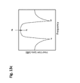
- the frequency response (in terms of the real impedance) of a conventional shunt resonator without an added parallel capacitance and the frequency response (in terms of real impedance) of an enhanced shunt resonator with an added parallel capacitance of 1.0 pF can be compared.
- the resonances of both the conventional acoustic resonator and the enhanced acoustic resonator are the same and are shown at marker m 1 (1.898 GHz).
- the upper Bragg Band frequencies of both the conventional acoustic resonator and the enhanced acoustic resonator are the same and are shown at markers m 4 and m 5 (2.028 GHz).
- the anti-resonance of the conventional acoustic resonator is shown at marker m 3 (1.964 GHz), while the anti-resonance of the enhanced acoustic resonator is shown at marker m 2 (1.964 GHz).
- the upper Bragg band frequency at marker m 4 is higher than the anti-resonant frequency at marker m 3 by 64 MHz
- the upper Bragg band frequency at marker m 5 is higher than the anti-resonant frequency at marker m 2 by 82 MHz.
- the lumped capacitive structures 260 avoid coupling the acoustic waves originating from the lumped resonator structures 258 . Furthermore, it is desirable that the lumped capacitive structures 260 be capable of handling high power without incurring damage. To this end, several novel designs of lumped capacitive structures 260 that avoid or minimize coupling acoustic waves originating from the interdigitated resonator fingers 266 and/or handle high power without incurring damage, will now be described.
- the following described lumped capacitive structures 260 are monolithically disposed on the piezoelectric layer 252 (which may, e.g., be a piezoelectric substrate or a thin-film piezoelectric monolithically disposed on a non-piezoelectric substrate) and are electrically coupled (e.g., in parallel) to the acoustic resonator structure 258 .
- the following lumped capacitive structures 260 are described as being electrically coupled between the metalized input signal plane portion 254 a and the metalized output signal plane portion 254 b , similar to the lumped capacitive structure 260 a illustrated in FIG. 11 b , although the following lumped capacitive structures 260 may be alternatively electrically coupled between the metalized signal plane 254 and the metalized ground plane 256 , similar to the lumped capacitive structure 260 b illustrated in FIG. 12 .
- the following described lumped capacitive structures 260 may be partially nested within, fully nested within, or not nested at all within, the metalized input signal plane portion 254 a , metalized output signal plane portion 254 b , metalized input signal plane 254 , or metalized ground plane 256 .
- one embodiment of a lumped capacitive structure 260 comprises an arrangement of planar interdigitated capacitive fingers 268 a .
- the orientation of the interdigitated capacitive fingers 268 a may be orthogonal to the orientation of the interdigitated resonator fingers 266 of the lumped resonator structure 258 a ( FIG. 19 a ), parallel to the orientation of the interdigitated resonator fingers 266 of the lumped resonator structure 258 a ( FIG. 19 b ), or oblique to the orientation of the interdigitated resonator fingers 266 of the lumped resonator structure 258 a ( FIG. 19 c ).
- Each of at least one of the interdigitated capacitive fingers 268 a (in the illustrated embodiment, all of the interdigitated capacitive fingers 268 a ) has an edge 270 that is entirely continuous (i.e., there are no discontinuities, such as sharp corners, along the entire edge).
- the edge 270 of each interdigitated capacitive finger 268 a takes the form of a single undulation. Because there are no discontinuities in the edges 270 of the interdigitated capacitive fingers 268 a , electrical power will not be concentrated or focused on any portions of the edges 270 .
- At least one of the interdigitated capacitive fingers 268 a (in the illustrated embodiment, all of the interdigitated capacitive fingers 268 a ) has a length (l)-to-width (w) ratio of less than two, and preferably, a length-to-width ratio of less than one. Furthermore, it should be appreciated that no finite portion of the edge 270 along the length of each of at least one of the interdigitated capacitive fingers 268 a (in the illustrated embodiment, all of the interdigitated capacitive fingers 268 a ) is parallel to any finite portions of edges 282 (in this case, the straight edges 282 ) along the lengths of the interdigitated resonator fingers 266 .
- FIG. 20 a -20 c another embodiment of a lumped capacitive structure 260 ( 2 ) comprises an arrangement of planar interdigitated capacitive fingers 268 b .
- the orientation of the interdigitated capacitive fingers 268 b may be orthogonal to the orientation of the interdigitated resonator fingers 266 of the lumped resonator structure 258 a ( FIG. 20 a ), parallel to the orientation of the interdigitated resonator fingers 266 of the lumped resonator structure 258 a ( FIG. 20 b ), or orthogonal to the orientation of the interdigitated resonator fingers 266 of the lumped resonator structure 258 a ( FIG. 20 c ).
- At least one of the interdigitated capacitive fingers 268 b (in the illustrated embodiment, all of the interdigitated capacitive fingers 268 b ) has a length (l)-to-width (w) ratio of less than two, and preferably, a length-to-width ratio of less than one.
- each of at least one of the interdigitated capacitive fingers 268 b (in the illustrated embodiment, all of the interdigitated capacitive fingers 268 b ) has straight edges 272 a , 272 b that takes the form of a single sawtooth instead of a single undulation.
- no finite portion of the edge 272 a , 272 b along the length of each of at least one of the interdigitated capacitive fingers 268 b is parallel to any finite portions of edges 282 (in this case, the straight edges 282 ) along the length of the interdigitated resonator fingers 266 .
- the straight edges 272 a , 272 b of each of the interdigitated capacitive fingers 268 b are oriented at a 45-degree angle relative to the orientation of the straight edges 282 of the interdigitated resonator fingers 266 .
- the edge 272 a of each of the interdigitated capacitive fingers 268 b is orthogonal to the straight edges 282 of each of the interdigitated capacitive fingers 268 b
- the edge 272 b of each of the interdigitated capacitive fingers 268 b is parallel to the straight edges 282 of each of the interdigitated capacitive fingers 268 b.
- FIGS. 19 and 20 lend themselves well to lumped capacitive structures 268 with relatively low static capacitance requirements. However, for lumped capacitive structures 268 with relatively high static capacitance requirements, the embodiments illustrated in FIGS. 21 and 22 may be used.
- a lumped capacitive structure 260 ( 3 ) comprises an arrangement of planar interdigitated capacitive fingers 268 c .
- the orientation of the interdigitated capacitive fingers 268 c may be orthogonal to the orientation of the interdigitated resonator fingers 266 of the lumped resonator structure 258 a ( FIG. 21 a ), parallel to the orientation of the interdigitated resonator fingers 266 of the lumped resonator structure 258 a ( FIG. 21 b ), or oblique to the orientation of the interdigitated resonator fingers 266 of the lumped resonator structure 258 a ( FIG. 21 c ).
- the lumped capacitive structure 260 ( 3 ) is similar to the embodiment illustrated in FIGS. 19 a -19 c , with the exception that each of the interdigitated capacitive fingers 268 c has an edge that forms a plurality of undulations, instead of a single undulation. In this manner, each of the interdigitated capacitive fingers 268 c comprises a plurality of interdigitated capacitive sub-fingers 274 , thereby increasing the effective lengths, and thus the static capacitances, of the interdigitated capacitive fingers 268 c . As can be seen in FIGS.
- all of the interdigitated capacitive sub-fingers 274 of each interdigitated capacitive finger 268 c have an orientation that is orthogonal to the orientation of the respective interdigitated capacitive finger 268 c .
- Each of the interdigitated capacitive sub-fingers 274 of each least one of the interdigitated capacitive fingers 268 c (in the illustrated embodiment, all of the interdigitated capacitive fingers 268 c ) has an edge 276 that is entirely continuous (i.e., there are no discontinuities, such as sharp corners). Because there are no discontinuities in the edges 276 of the interdigitated capacitive sub-fingers 274 , electrical power will not be concentrated or focused on any portions of the edges 276 .
- No finite portion of the edge 276 along each of at least one of the interdigitated capacitive sub-fingers 274 is parallel to any finite portions of edges 282 (in this case, the straight edges 282 ) along the lengths of the interdigitated resonator fingers 266 . This remains true regardless the orientation of the orientation of the interdigitated capacitive fingers 268 a relative to the orientation of the interdigitated resonator fingers 266 of the lumped resonator structure 258 a , as can be seen in FIGS. 21 a -21 c .
- yet another embodiment of a lumped capacitive structure 260 comprises an arrangement of planar interdigitated capacitive fingers 268 d .
- the orientation of the interdigitated capacitive fingers 268 d may be orthogonal to the orientation of the interdigitated resonator fingers 266 of the lumped resonator structure 258 a ( FIG. 22 a ), parallel to the orientation of the interdigitated resonator fingers 266 of the lumped resonator structure 258 a ( FIG. 22 b ), or oblique to the orientation of the interdigitated resonator fingers 266 of the lumped resonator structure 258 a ( FIG. 22 c ).
- each of the interdigitated capacitive fingers 268 d shown in FIGS. 22 a -22 c comprises a plurality of interdigitated capacitive sub-fingers 278 , thereby increasing the effective lengths, and thus the static capacitances, of the interdigitated capacitive fingers 268 d .
- all of the interdigitated capacitive sub-fingers 278 of each interdigitated capacitive finger 268 d have an orientation that is orthogonal to the orientation of the respective interdigitated capacitive finger 268 d .
- each interdigitated capacitive sub-finger 278 has two straight edges 280 a , 280 b that forms a sawtooth.
- no finite portion of the straight edges 280 a , 280 b along the length of each of at least one of the interdigitated capacitive sub-fingers 278 is parallel to any finite portions of edges 282 (in this case, the straight edges 282 ) along the length of the interdigitated resonator fingers 266 .
- the straight edges 280 a , 280 b of each of the interdigitated capacitive sub-fingers 278 are oriented at a 45-degree angle relative to the orientation of the straight edges 282 of the interdigitated resonator fingers 266 .
- the edge 280 a of each of the interdigitated capacitive sub-fingers 278 is orthogonal to the straight edges 282 along the length of the interdigitated resonator fingers 266
- the edge 280 b of each of the interdigitated capacitive sub-fingers 278 is parallel to the straight edges 282 along the length of the interdigitated resonator fingers 266 .
Landscapes
- Physics & Mathematics (AREA)
- Acoustics & Sound (AREA)
- Chemical & Material Sciences (AREA)
- Crystallography & Structural Chemistry (AREA)
- Surface Acoustic Wave Elements And Circuit Networks Thereof (AREA)
- Piezo-Electric Or Mechanical Vibrators, Or Delay Or Filter Circuits (AREA)
Abstract
Description
where ωR and ωA may be the respective resonance and anti-resonance frequencies for any given acoustic resonator, and gamma γ may depend on a material's property, which may be further defined by:
It can be appreciated from equation [1] that the resonant frequency of each of the acoustic resonators will depend on the motional arm of the
wherein f is the frequency in hertz, L is the inductance in henrys, and C is the capacitance in farads, the transmission zeroes and reflection zeroes of the equivalent filter circuit of
This resonance creates an effective short circuit to the return path and no power is transmitted from the input to the output of the filter. One reflection zero located in the passband is effectively the resonance created by the circuit Lm1, Cm1, and C01 (i.e., the anti-resonance of the acoustic resonator ZP) and is given by:
This resonance creates an effective open circuit to the return path, allowing power to be transmitted from the input to the output of the filter. The other reflection zero located in the passband is effectively the resonance created by the circuit Lm2 and Cm2 (i.e., the resonance of the acoustic resonator ZS) and is given by:
This resonance creates an effective short circuit, allowing power to be transmitted from the input to the output of the filter. The transmission zero at the upper edge of the passband is effectively the resonance created by the circuit Lm2, Cm2, and C02 (i.e., the anti-resonance of the acoustic resonator ZS) and is given by:
This resonance creates an effective open circuit to the return path, preventing power from being transmitted from the input to the output of the filter.
The relationship between the reflection zero Fb in equation [6] and the reflection zero Fb′ in equation [9] can be determined by assigning values to the lumped elements and solving equations [6] and [9]. Setting Lm1=Cm1=C01=1, then
where k is a constant. When Csh=0, Fb=Fb′. For any positive values of Csh, then Fb′<Fb.
The relationship between the transmission zero Fd in equation [8] and the transmission zero Fd′ in equation [10] can be determined by assigning values to the lumped elements and solving equations [8] and [10]. Setting Lm2=Cm2=C02=1, then
where k is a constant. When Cse=0, Fd=Fd′. For any positive values of Cse, then Fd′<Fd.
Claims (22)
Priority Applications (4)
| Application Number | Priority Date | Filing Date | Title |
|---|---|---|---|
| US15/443,740 US10305447B2 (en) | 2015-11-13 | 2017-02-27 | Acoustic wave filter with enhanced rejection |
| PCT/US2018/019899 WO2018157114A1 (en) | 2017-02-27 | 2018-02-27 | Acoustic wave filter with enhanced rejection |
| DE112018001025.2T DE112018001025T5 (en) | 2017-02-27 | 2018-02-27 | Acoustic wave filter with increased rejection |
| CN201880012977.1A CN110506391B (en) | 2017-02-27 | 2018-02-27 | Acoustic wave filter with enhanced suppression |
Applications Claiming Priority (2)
| Application Number | Priority Date | Filing Date | Title |
|---|---|---|---|
| US14/941,451 US9608595B1 (en) | 2015-11-13 | 2015-11-13 | Acoustic wave filter with enhanced rejection |
| US15/443,740 US10305447B2 (en) | 2015-11-13 | 2017-02-27 | Acoustic wave filter with enhanced rejection |
Related Parent Applications (1)
| Application Number | Title | Priority Date | Filing Date |
|---|---|---|---|
| US14/941,451 Continuation-In-Part US9608595B1 (en) | 2015-11-13 | 2015-11-13 | Acoustic wave filter with enhanced rejection |
Publications (2)
| Publication Number | Publication Date |
|---|---|
| US20170179928A1 US20170179928A1 (en) | 2017-06-22 |
| US10305447B2 true US10305447B2 (en) | 2019-05-28 |
Family
ID=59065286
Family Applications (1)
| Application Number | Title | Priority Date | Filing Date |
|---|---|---|---|
| US15/443,740 Active 2036-02-04 US10305447B2 (en) | 2015-11-13 | 2017-02-27 | Acoustic wave filter with enhanced rejection |
Country Status (1)
| Country | Link |
|---|---|
| US (1) | US10305447B2 (en) |
Cited By (18)
| Publication number | Priority date | Publication date | Assignee | Title |
|---|---|---|---|---|
| US20220247382A1 (en) * | 2021-02-03 | 2022-08-04 | Resonant Inc. | Bandpass filters using transversely-excited film bulk acoustic resonators |
| US12095446B2 (en) | 2018-06-15 | 2024-09-17 | Murata Manufacturing Co., Ltd. | Transversely-excited film bulk acoustic resonator with optimized electrode thickness, mark, and pitch |
| US12107568B2 (en) | 2021-03-24 | 2024-10-01 | Murata Manufacturing Co., Ltd. | Composite transversely-excited film bulk acoustic resonator circuits having a capacitor for improved rejection |
| US12166468B2 (en) | 2021-01-15 | 2024-12-10 | Murata Manufacturing Co., Ltd. | Decoupled transversely-excited film bulk acoustic resonators for high power filters |
| US12176878B2 (en) | 2018-06-15 | 2024-12-24 | Murata Manufacturing Co., Ltd. | Solidly-mounted transversely-excited film bulk acoustic resonator with recessed interdigital transducer fingers |
| US12244295B2 (en) | 2018-06-15 | 2025-03-04 | Murata Manufacturing Co., Ltd. | Transversely-excited film bulk acoustic resonators with two-layer electrodes having a narrower top layer |
| US12244299B2 (en) | 2018-06-15 | 2025-03-04 | Murata Manufacturing Co., Ltd. | Transversely-excited film bulk acoustic resonator with periodic etched holes |
| US12255605B2 (en) | 2020-06-18 | 2025-03-18 | Murata Manufacturing Co., Ltd. | Transversely-excited film bulk acoustic resonators with electrodes having a second layer of variable width |
| US12283938B2 (en) | 2021-01-15 | 2025-04-22 | Murata Manufacturing Co., Ltd. | Decoupled transversely-excited film bulk acoustic resonators |
| US12289094B2 (en) | 2020-06-30 | 2025-04-29 | Murata Manufacturing Co., Ltd. | Transversely-excited film bulk acoustic resonator with symmetric diaphragm |
| US12301204B2 (en) | 2018-06-15 | 2025-05-13 | Murata Manufacturing Co., Ltd. | Solidly-mounted transversely-excited film bulk acoustic resonator |
| US12308823B2 (en) | 2018-06-15 | 2025-05-20 | Murata Manufacturing Co., Ltd. | Transversely-excited film bulk acoustic filters with symmetric layout |
| US12375062B2 (en) | 2020-02-28 | 2025-07-29 | Murata Manufacturing Co., Ltd. | Transversely-excited film bulk acoustic resonator filters with sub-resonators having different mark and pitch |
| US12375061B2 (en) | 2020-10-05 | 2025-07-29 | Murata Manufacturing Co., Ltd. | Transversely-excited film bulk acoustic resonator matrix filters |
| US12375056B2 (en) | 2018-06-15 | 2025-07-29 | Murata Manufacturing Co., Ltd. | Transversely-excited film bulk acoustic resonators |
| US12413196B2 (en) | 2022-02-16 | 2025-09-09 | Murata Manufacturing Co., Ltd. | Tuning acoustic resonators with back-side coating |
| US12424999B2 (en) | 2021-12-28 | 2025-09-23 | Murata Manufacturing Co., Ltd. | Transversely-excited film bulk acoustic resonators with gap dielectric stripes in busbar-electrode gaps |
| US12549151B2 (en) | 2022-04-12 | 2026-02-10 | Murata Manufacturing Co., Ltd. | Transversely-excited film bulk acoustic resonator with thick dielectric layer for improved coupling |
Families Citing this family (138)
| Publication number | Priority date | Publication date | Assignee | Title |
|---|---|---|---|---|
| DE112018001025T5 (en) * | 2017-02-27 | 2020-07-02 | Resonant Inc. (n.d.Ges.d. Staates Delaware) | Acoustic wave filter with increased rejection |
| US11996827B2 (en) | 2018-06-15 | 2024-05-28 | Murata Manufacturing Co., Ltd. | Transversely-excited film bulk acoustic resonator with periodic etched holes |
| US10637438B2 (en) | 2018-06-15 | 2020-04-28 | Resonant Inc. | Transversely-excited film bulk acoustic resonators for high power applications |
| US12237826B2 (en) | 2018-06-15 | 2025-02-25 | Murata Manufacturing Co., Ltd. | Transversely-excited film bulk acoustic resonator with optimized electrode thickness, mark, and pitch |
| US10790802B2 (en) | 2018-06-15 | 2020-09-29 | Resonant Inc. | Transversely excited film bulk acoustic resonator using rotated Y-X cut lithium niobate |
| US10491192B1 (en) | 2018-06-15 | 2019-11-26 | Resonant Inc. | Transversely-excited film bulk acoustic resonator |
| US11206009B2 (en) | 2019-08-28 | 2021-12-21 | Resonant Inc. | Transversely-excited film bulk acoustic resonator with interdigital transducer with varied mark and pitch |
| US10601392B2 (en) | 2018-06-15 | 2020-03-24 | Resonant Inc. | Solidly-mounted transversely-excited film bulk acoustic resonator |
| US11936358B2 (en) | 2020-11-11 | 2024-03-19 | Murata Manufacturing Co., Ltd. | Transversely-excited film bulk acoustic resonator with low thermal impedance |
| US10756697B2 (en) | 2018-06-15 | 2020-08-25 | Resonant Inc. | Transversely-excited film bulk acoustic resonator |
| US11323090B2 (en) | 2018-06-15 | 2022-05-03 | Resonant Inc. | Transversely-excited film bulk acoustic resonator using Y-X-cut lithium niobate for high power applications |
| US11146232B2 (en) | 2018-06-15 | 2021-10-12 | Resonant Inc. | Transversely-excited film bulk acoustic resonator with reduced spurious modes |
| US11323089B2 (en) | 2018-06-15 | 2022-05-03 | Resonant Inc. | Filter using piezoelectric film bonded to high resistivity silicon substrate with trap-rich layer |
| US12040779B2 (en) | 2020-04-20 | 2024-07-16 | Murata Manufacturing Co., Ltd. | Small transversely-excited film bulk acoustic resonators with enhanced Q-factor |
| US12088281B2 (en) | 2021-02-03 | 2024-09-10 | Murata Manufacturing Co., Ltd. | Transversely-excited film bulk acoustic resonator with multi-mark interdigital transducer |
| US10911023B2 (en) | 2018-06-15 | 2021-02-02 | Resonant Inc. | Transversely-excited film bulk acoustic resonator with etch-stop layer |
| US11929731B2 (en) | 2018-02-18 | 2024-03-12 | Murata Manufacturing Co., Ltd. | Transversely-excited film bulk acoustic resonator with optimized electrode mark, and pitch |
| US11509279B2 (en) | 2020-07-18 | 2022-11-22 | Resonant Inc. | Acoustic resonators and filters with reduced temperature coefficient of frequency |
| WO2019226683A1 (en) * | 2018-05-25 | 2019-11-28 | Skyworks Solutions, Inc. | Filter including acoustic wave resonator in parallel with circuit element |
| US11264966B2 (en) | 2018-06-15 | 2022-03-01 | Resonant Inc. | Solidly-mounted transversely-excited film bulk acoustic resonator with diamond layers in Bragg reflector stack |
| US10998882B2 (en) | 2018-06-15 | 2021-05-04 | Resonant Inc. | XBAR resonators with non-rectangular diaphragms |
| US10985728B2 (en) | 2018-06-15 | 2021-04-20 | Resonant Inc. | Transversely-excited film bulk acoustic resonator and filter with a uniform-thickness dielectric overlayer |
| US11171629B2 (en) | 2018-06-15 | 2021-11-09 | Resonant Inc. | Transversely-excited film bulk acoustic resonator using pre-formed cavities |
| US11967945B2 (en) | 2018-06-15 | 2024-04-23 | Murata Manufacturing Co., Ltd. | Transversly-excited film bulk acoustic resonators and filters |
| US10917072B2 (en) | 2019-06-24 | 2021-02-09 | Resonant Inc. | Split ladder acoustic wave filters |
| US12463619B2 (en) | 2018-06-15 | 2025-11-04 | Murata Manufacturing Co., Ltd. | Filter device |
| US12301212B2 (en) | 2018-06-15 | 2025-05-13 | Murata Manufacturing Co., Ltd. | XBAR resonators with non-rectangular diaphragms |
| US12040781B2 (en) | 2018-06-15 | 2024-07-16 | Murata Manufacturing Co., Ltd. | Transversely-excited film bulk acoustic resonator package |
| US11201601B2 (en) | 2018-06-15 | 2021-12-14 | Resonant Inc. | Transversely-excited film bulk acoustic resonator with multiple diaphragm thicknesses and fabrication method |
| US11901878B2 (en) | 2018-06-15 | 2024-02-13 | Murata Manufacturing Co., Ltd. | Transversely-excited film bulk acoustic resonators with two-layer electrodes with a wider top layer |
| US11909381B2 (en) | 2018-06-15 | 2024-02-20 | Murata Manufacturing Co., Ltd. | Transversely-excited film bulk acoustic resonators with two-layer electrodes having a narrower top layer |
| US12155374B2 (en) | 2021-04-02 | 2024-11-26 | Murata Manufacturing Co., Ltd. | Tiled transversely-excited film bulk acoustic resonator high power filters |
| US11146238B2 (en) | 2018-06-15 | 2021-10-12 | Resonant Inc. | Film bulk acoustic resonator fabrication method |
| US10797675B2 (en) | 2018-06-15 | 2020-10-06 | Resonant Inc. | Transversely excited film bulk acoustic resonator using rotated z-cut lithium niobate |
| US11996822B2 (en) | 2018-06-15 | 2024-05-28 | Murata Manufacturing Co., Ltd. | Wide bandwidth time division duplex transceiver |
| US12218650B2 (en) | 2018-06-15 | 2025-02-04 | Murata Manufacturing Co., Ltd. | Transversely-excited film bulk acoustic resonator |
| US11323095B2 (en) | 2018-06-15 | 2022-05-03 | Resonant Inc. | Rotation in XY plane to suppress spurious modes in XBAR devices |
| US12021496B2 (en) | 2020-08-31 | 2024-06-25 | Murata Manufacturing Co., Ltd. | Resonators with different membrane thicknesses on the same die |
| US12155371B2 (en) | 2021-03-29 | 2024-11-26 | Murata Manufacturing Co., Ltd. | Layout of xbars with multiple sub-resonators in series |
| US12224732B2 (en) | 2018-06-15 | 2025-02-11 | Murata Manufacturing Co., Ltd. | Solidly-mounted transversely-excited film bulk acoustic resonators and filters for 27 GHz communications bands |
| US11949402B2 (en) | 2020-08-31 | 2024-04-02 | Murata Manufacturing Co., Ltd. | Resonators with different membrane thicknesses on the same die |
| US11374549B2 (en) | 2018-06-15 | 2022-06-28 | Resonant Inc. | Filter using transversely-excited film bulk acoustic resonators with divided frequency-setting dielectric layers |
| US11323091B2 (en) | 2018-06-15 | 2022-05-03 | Resonant Inc. | Transversely-excited film bulk acoustic resonator with diaphragm support pedestals |
| US11329628B2 (en) | 2020-06-17 | 2022-05-10 | Resonant Inc. | Filter using lithium niobate and lithium tantalate transversely-excited film bulk acoustic resonators |
| US10826462B2 (en) | 2018-06-15 | 2020-11-03 | Resonant Inc. | Transversely-excited film bulk acoustic resonators with molybdenum conductors |
| US10992284B2 (en) | 2018-06-15 | 2021-04-27 | Resonant Inc. | Filter using transversely-excited film bulk acoustic resonators with multiple frequency setting layers |
| US11349450B2 (en) | 2018-06-15 | 2022-05-31 | Resonant Inc. | Symmetric transversely-excited film bulk acoustic resonators with reduced spurious modes |
| US12283944B2 (en) | 2018-06-15 | 2025-04-22 | Murata Manufacturing Co., Ltd. | Transversely-excited film bulk acoustic resonator with recessed rotated-Y-X cut lithium niobate |
| US12009798B2 (en) | 2018-06-15 | 2024-06-11 | Murata Manufacturing Co., Ltd. | Transversely-excited film bulk acoustic resonators with electrodes having irregular hexagon cross-sectional shapes |
| US11876498B2 (en) | 2018-06-15 | 2024-01-16 | Murata Manufacturing Co., Ltd. | Transversely-excited film bulk acoustic resonator with multiple diaphragm thicknesses and fabrication method |
| US10819309B1 (en) | 2019-04-05 | 2020-10-27 | Resonant Inc. | Transversely-excited film bulk acoustic resonator package and method |
| US12184261B2 (en) | 2018-06-15 | 2024-12-31 | Murata Manufacturing Co., Ltd. | Transversely-excited film bulk acoustic resonator with a cavity having round end zones |
| US12170516B2 (en) | 2018-06-15 | 2024-12-17 | Murata Manufacturing Co., Ltd. | Filters using transversly-excited film bulk acoustic resonators with frequency-setting dielectric layers |
| US11888463B2 (en) | 2018-06-15 | 2024-01-30 | Murata Manufacturing Co., Ltd. | Multi-port filter using transversely-excited film bulk acoustic resonators |
| US10868513B2 (en) | 2018-06-15 | 2020-12-15 | Resonant Inc. | Transversely-excited film bulk acoustic filters with symmetric layout |
| US10998877B2 (en) | 2018-06-15 | 2021-05-04 | Resonant Inc. | Film bulk acoustic resonator fabrication method with frequency trimming based on electric measurements prior to cavity etch |
| US12191838B2 (en) | 2018-06-15 | 2025-01-07 | Murata Manufacturing Co., Ltd. | Solidly-mounted transversely-excited film bulk acoustic device and method |
| US11996825B2 (en) | 2020-06-17 | 2024-05-28 | Murata Manufacturing Co., Ltd. | Filter using lithium niobate and rotated lithium tantalate transversely-excited film bulk acoustic resonators |
| US10992283B2 (en) | 2018-06-15 | 2021-04-27 | Resonant Inc. | High power transversely-excited film bulk acoustic resonators on rotated Z-cut lithium niobate |
| US11728785B2 (en) | 2018-06-15 | 2023-08-15 | Murata Manufacturing Co., Ltd. | Transversely-excited film bulk acoustic resonator using pre-formed cavities |
| US12119808B2 (en) | 2018-06-15 | 2024-10-15 | Murata Manufacturing Co., Ltd. | Transversely-excited film bulk acoustic resonator package |
| US12081187B2 (en) | 2018-06-15 | 2024-09-03 | Murata Manufacturing Co., Ltd. | Transversely-excited film bulk acoustic resonator |
| US11228296B2 (en) | 2018-06-15 | 2022-01-18 | Resonant Inc. | Transversely-excited film bulk acoustic resonator with a cavity having a curved perimeter |
| US12149227B2 (en) | 2018-06-15 | 2024-11-19 | Murata Manufacturing Co., Ltd. | Transversely-excited film bulk acoustic resonator package |
| US12191837B2 (en) | 2018-06-15 | 2025-01-07 | Murata Manufacturing Co., Ltd. | Solidly-mounted transversely-excited film bulk acoustic device |
| US12113512B2 (en) | 2021-03-29 | 2024-10-08 | Murata Manufacturing Co., Ltd. | Layout of XBARs with multiple sub-resonators in parallel |
| US12212306B2 (en) | 2018-06-15 | 2025-01-28 | Murata Manufacturing Co., Ltd. | Transversely-excited film bulk acoustic resonator with multiple diaphragm thicknesses and fabrication method |
| US12237827B2 (en) | 2018-06-15 | 2025-02-25 | Murata Manufacturing Co., Ltd. | Solidly-mounted transversely-excited film bulk acoustic filters with multiple piezoelectric plate thicknesses |
| US12119805B2 (en) | 2018-06-15 | 2024-10-15 | Murata Manufacturing Co., Ltd. | Substrate processing and membrane release of transversely-excited film bulk acoustic resonator using a sacrificial tub |
| US11870423B2 (en) | 2018-06-15 | 2024-01-09 | Murata Manufacturing Co., Ltd. | Wide bandwidth temperature-compensated transversely-excited film bulk acoustic resonator |
| US11901873B2 (en) | 2019-03-14 | 2024-02-13 | Murata Manufacturing Co., Ltd. | Transversely-excited film bulk acoustic resonator with partial BRAGG reflectors |
| CN113615083B (en) | 2019-03-14 | 2024-10-15 | 株式会社村田制作所 | Laterally excited film bulk acoustic resonator with half-λ dielectric layer |
| US10911021B2 (en) | 2019-06-27 | 2021-02-02 | Resonant Inc. | Transversely-excited film bulk acoustic resonator with lateral etch stop |
| US12034423B2 (en) | 2019-06-27 | 2024-07-09 | Murata Manufacturing Co., Ltd | XBAR frontside etch process using polysilicon sacrificial layer |
| US10862454B1 (en) | 2019-07-18 | 2020-12-08 | Resonant Inc. | Film bulk acoustic resonators in thin LN-LT layers |
| US11329625B2 (en) | 2019-07-18 | 2022-05-10 | Resonant Inc. | Film bulk acoustic sensors using thin LN-LT layer |
| EP4042567A4 (en) * | 2019-10-07 | 2023-07-05 | Intel Corporation | HYBRID RESONATORS |
| CN115004550A (en) * | 2020-01-24 | 2022-09-02 | 株式会社村田制作所 | Filter device, multiplexer, high-frequency front-end circuit, and communication device |
| WO2021153458A1 (en) * | 2020-01-31 | 2021-08-05 | 株式会社村田製作所 | Multiplexer |
| JP7405159B2 (en) * | 2020-01-31 | 2023-12-26 | 株式会社村田製作所 | multiplexer |
| US12506462B2 (en) | 2020-02-28 | 2025-12-23 | Murata Manufacturing Co., Ltd. | Transversely-excited film bulk acoustic resonator with multi-pitch interdigital transducer |
| US12255625B2 (en) | 2020-02-28 | 2025-03-18 | Murata Manufacturing Co., Ltd. | Filter using transversely-excited film bulk acoustic resonators with inductively coupled sub-resonators |
| US12278617B2 (en) | 2020-04-20 | 2025-04-15 | Murata Manufacturing Co., Ltd. | High Q solidly-mounted transversely-excited film bulk acoustic resonators |
| US12341493B2 (en) | 2020-04-20 | 2025-06-24 | Murata Manufacturing Co., Ltd. | Low loss transversely-excited film bulk acoustic resonators and filters |
| US12341490B2 (en) | 2020-04-20 | 2025-06-24 | Murata Manufacturing Co., Ltd. | Low loss transversely-excited film bulk acoustic resonators and filters |
| US11811391B2 (en) | 2020-05-04 | 2023-11-07 | Murata Manufacturing Co., Ltd. | Transversely-excited film bulk acoustic resonator with etched conductor patterns |
| US11469733B2 (en) | 2020-05-06 | 2022-10-11 | Resonant Inc. | Transversely-excited film bulk acoustic resonators with interdigital transducer configured to reduce diaphragm stress |
| US12074584B2 (en) | 2020-05-28 | 2024-08-27 | Murata Manufacturing Co., Ltd. | Transversely-excited film bulk acoustic resonators with two-layer electrodes |
| US12267062B2 (en) | 2020-06-17 | 2025-04-01 | Murata Manufacturing Co., Ltd. | Transversely-excited film bulk acoustic resonators with three-layer electrodes |
| US11482981B2 (en) | 2020-07-09 | 2022-10-25 | Resonanat Inc. | Transversely-excited film bulk acoustic resonators with piezoelectric diaphragm supported by piezoelectric substrate |
| US11264969B1 (en) | 2020-08-06 | 2022-03-01 | Resonant Inc. | Transversely-excited film bulk acoustic resonator comprising small cells |
| US11271539B1 (en) | 2020-08-19 | 2022-03-08 | Resonant Inc. | Transversely-excited film bulk acoustic resonator with tether-supported diaphragm |
| US11671070B2 (en) | 2020-08-19 | 2023-06-06 | Murata Manufacturing Co., Ltd. | Transversely-excited film bulk acoustic resonators using multiple dielectric layer thicknesses to suppress spurious modes |
| US11894835B2 (en) | 2020-09-21 | 2024-02-06 | Murata Manufacturing Co., Ltd. | Sandwiched XBAR for third harmonic operation |
| US11476834B2 (en) | 2020-10-05 | 2022-10-18 | Resonant Inc. | Transversely-excited film bulk acoustic resonator matrix filters with switches in parallel with sub-filter shunt capacitors |
| US11405017B2 (en) | 2020-10-05 | 2022-08-02 | Resonant Inc. | Acoustic matrix filters and radios using acoustic matrix filters |
| US11728784B2 (en) | 2020-10-05 | 2023-08-15 | Murata Manufacturing Co., Ltd. | Transversely-excited film bulk acoustic resonator matrix filters with split die sub-filters |
| US11929733B2 (en) | 2020-10-05 | 2024-03-12 | Murata Manufacturing Co., Ltd. | Transversely-excited film bulk acoustic resonator matrix filters with input and output impedances matched to radio frequency front end elements |
| US11658639B2 (en) | 2020-10-05 | 2023-05-23 | Murata Manufacturing Co., Ltd. | Transversely-excited film bulk acoustic resonator matrix filters with noncontiguous passband |
| US11463066B2 (en) | 2020-10-14 | 2022-10-04 | Resonant Inc. | Transversely-excited film bulk acoustic resonators with piezoelectric diaphragm supported by piezoelectric substrate |
| US12119806B2 (en) | 2020-10-30 | 2024-10-15 | Murata Manufacturing Co., Ltd. | Transversely-excited film bulk acoustic resonator with spiral interdigitated transducer fingers |
| US12003226B2 (en) | 2020-11-11 | 2024-06-04 | Murata Manufacturing Co., Ltd | Transversely-excited film bulk acoustic resonator with low thermal impedance |
| US12255617B2 (en) | 2020-11-11 | 2025-03-18 | Murata Manufacturing Co., Ltd. | Solidly-mounted transversely-excited film bulk acoustic resonators with low thermal impedance |
| US12431856B2 (en) | 2020-11-12 | 2025-09-30 | Murata Manufacturing Co., Ltd. | Transversely-excited film bulk acoustic resonator with reduced loss in the aperture direction |
| US12028039B2 (en) | 2020-11-13 | 2024-07-02 | Murata Manufacturing Co., Ltd. | Forming XBAR devices with excess piezoelectric material removed |
| US12362725B2 (en) | 2020-11-13 | 2025-07-15 | Murata Manufacturing Co., Ltd. | Transversely-excited film bulk acoustic filters with excess piezoelectric material removed |
| US11496113B2 (en) | 2020-11-13 | 2022-11-08 | Resonant Inc. | XBAR devices with excess piezoelectric material removed |
| US12255626B2 (en) | 2020-11-13 | 2025-03-18 | Murata Manufacturing Co., Ltd. | Solidly-mounted transversely-excited film bulk acoustic filters with excess piezoelectric material removed |
| US11405020B2 (en) | 2020-11-26 | 2022-08-02 | Resonant Inc. | Transversely-excited film bulk acoustic resonators with structures to reduce acoustic energy leakage |
| WO2022124391A1 (en) * | 2020-12-11 | 2022-06-16 | 株式会社村田製作所 | Elastic wave device |
| US12126318B2 (en) | 2021-01-15 | 2024-10-22 | Murata Manufacturing Co., Ltd. | Filters using decoupled transversely-excited film bulk acoustic resonators |
| US12463615B2 (en) | 2021-01-21 | 2025-11-04 | Murata Manufacturing Co., Ltd | Transversely-excited film bulk acoustic resonators with improved coupling and reduced energy leakage |
| US12113510B2 (en) | 2021-02-03 | 2024-10-08 | Murata Manufacturing Co., Ltd. | Transversely-excited film bulk acoustic resonators with multiple piezoelectric membrane thicknesses on the same chip |
| US12308825B2 (en) | 2021-02-12 | 2025-05-20 | Murata Manufacturing Co., Ltd | Transversely-excited film bulk acoustic resonators with narrow gaps between busbars and ends of interdigital transducer fingers |
| US12289099B2 (en) | 2021-03-24 | 2025-04-29 | Murata Manufacturing Co., Ltd. | Acoustic filters with shared acoustic tracks for series and shunt resonators |
| US12126328B2 (en) | 2021-03-24 | 2024-10-22 | Murata Manufacturing Co., Ltd. | Acoustic filters with shared acoustic tracks |
| US12348216B2 (en) | 2021-03-24 | 2025-07-01 | Murata Manufacturing Co., Ltd. | Acoustic filters with shared acoustic tracks and cascaded series resonators |
| US12355426B2 (en) | 2021-03-24 | 2025-07-08 | Murata Manufacturing Co., Ltd. | Acoustic filters with shared acoustic tracks |
| US12341492B2 (en) | 2021-03-29 | 2025-06-24 | Murata Manufacturing Co., Ltd. | Transversely-excited film bulk acoustic resonators with busbar side edges that form angles with a perimeter of the cavity |
| US12224735B2 (en) | 2021-03-30 | 2025-02-11 | Murata Manufacturing Co., Ltd. | Diplexer using decoupled transversely-excited film bulk acoustic resonators |
| CN120454674A (en) | 2021-03-30 | 2025-08-08 | 株式会社村田制作所 | Filter for 6 GHz Wi-Fi using laterally excited film bulk acoustic resonators |
| US12249971B2 (en) | 2021-04-02 | 2025-03-11 | Murata Manufacturing Co., Ltd. | Transversely-excited film bulk acoustic resonators with solidly mounted resonator (SMR) pedestals |
| US12237823B2 (en) | 2021-04-02 | 2025-02-25 | Murata Manufacturing Co., Ltd. | Transversely-excited film bulk acoustic resonators with solidly mounted resonator (SMR) pedestals |
| US12255633B2 (en) | 2021-04-16 | 2025-03-18 | Murata Manufacturing Co., Ltd. | Filter using transversely-excited film bulk acoustic resonators |
| US12126316B2 (en) | 2021-04-16 | 2024-10-22 | Murata Manufacturing Co., Ltd | Transversely-excited film bulk acoustic resonator |
| US12160220B2 (en) | 2021-04-30 | 2024-12-03 | Murata Manufacturing Co., Ltd. | Transversely-excited film bulk acoustic resonator with oxide strip acoustic confinement structures |
| US12255607B2 (en) | 2021-04-30 | 2025-03-18 | Murata Manufacturing Co., Ltd. | Transversely-excited film bulk acoustic resonator with buried oxide strip acoustic confinement structures |
| US12075700B2 (en) | 2021-05-07 | 2024-08-27 | Murata Manufacturing Co., Ltd. | Transversely-excited film bulk acoustic resonator fabrication using polysilicon pillars |
| US12057823B2 (en) | 2021-05-07 | 2024-08-06 | Murata Manufacturing Co., Ltd. | Transversely-excited film bulk acoustic resonator with concentric interdigitated transducer fingers |
| US12170513B2 (en) | 2021-06-30 | 2024-12-17 | Murata Manufacturing Co., Ltd. | Transversely-excited film bulk acoustic resonator with reduced substrate to contact bump thermal resistance |
| US12603639B2 (en) | 2021-08-02 | 2026-04-14 | Murata Manufacturing Co., Ltd. | Metal cavity for transversely-excited film bulk acoustic resonator (XBAR) |
| US12456962B2 (en) | 2021-09-24 | 2025-10-28 | Murata Manufacturing Co., Ltd. | Transversely-excited film bulk acoustic resonators wafer-level packaging using a dielectric cover |
| US12225387B2 (en) | 2021-09-29 | 2025-02-11 | Murata Manufacturing Co., Ltd. | Communications device with concurrent operation in 5GHZ and 6GHZ U-NII frequency ranges |
| US12451864B2 (en) | 2021-09-29 | 2025-10-21 | Murata Manufacturing Co., Ltd. | Transversely-excited film bulk acoustic resonators with curved shaped ends of fingers or opposing busbars |
| US12407326B2 (en) | 2021-11-04 | 2025-09-02 | Murata Manufacturing Co., Ltd. | Stacked die transversely-excited film bulk acoustic resonator (XBAR) filters |
| US12494768B2 (en) | 2021-12-28 | 2025-12-09 | Murata Manufacturing Co., Ltd. | Transversely-excited film bulk acoustic resonators with gap dielectric stripes in busbar-electrode gaps |
| US12489417B2 (en) | 2022-04-12 | 2025-12-02 | Murata Manufacturing Co., Ltd. | Ladder filter with transversely-excited film bulk acoustic resonators having different pitches |
| US12489415B2 (en) | 2022-10-19 | 2025-12-02 | Murata Manufacturing Co., Ltd. | Acoustic resonator lid for thermal transport |
Citations (18)
| Publication number | Priority date | Publication date | Assignee | Title |
|---|---|---|---|---|
| JPH0522074A (en) | 1991-07-11 | 1993-01-29 | Hitachi Ltd | Surface acoustic wave resonator, surface acoustic wave resonator composite filter, and wireless transceiver |
| JPH0865089A (en) | 1994-08-22 | 1996-03-08 | Fujitsu Ltd | Surface acoustic wave filter |
| US5821834A (en) | 1997-03-05 | 1998-10-13 | Northern Telecom Limited | Surface wave device with capacitance |
| US5933062A (en) | 1997-11-04 | 1999-08-03 | Motorola Inc. | Acoustic wave ladder filter with effectively increased coupling coefficient and method of providing same |
| US6018281A (en) | 1995-03-15 | 2000-01-25 | Matsushita Electric Industrial Co., Ltd. | Resonator type surface acoustic wave ladder filter with voltage variable capacitance element |
| US6043585A (en) | 1996-03-29 | 2000-03-28 | Nokia Mobile Phones Limited | Acoustic wave filter |
| JP2001044792A (en) | 1999-07-30 | 2001-02-16 | Kyocera Corp | Surface acoustic wave device and band frequency adjustment method thereof |
| JP2002299997A (en) | 2001-03-30 | 2002-10-11 | Kyocera Corp | Surface acoustic wave filter |
| US6593678B1 (en) | 2000-10-24 | 2003-07-15 | Clarisay, Inc. | Surface acoustic wave filter having diminished bandwidth and method of operating the same |
| US6653913B2 (en) | 2000-04-06 | 2003-11-25 | Koninklijke Philips Electronics N.V. | Tunable piezoelectric filter arrangement using a dielectric material with a voltage-dependent dielectric constant |
| US20050212612A1 (en) | 2004-01-30 | 2005-09-29 | Kabushiki Kaisha Toshiba | Tunable filter and portable telephone |
| US7034638B2 (en) | 2002-09-18 | 2006-04-25 | Nihon Dempa Kogyo Co., Ltd. | SAW filter |
| US7616079B2 (en) | 2002-10-08 | 2009-11-10 | Epcos Ag | Bulk acoustic wave resonator and circuit comprising same |
| US8179211B2 (en) | 2005-07-08 | 2012-05-15 | Epcos Ag | RF-filter with improved adjacent channel suppression |
| EP2530837A1 (en) | 2010-01-28 | 2012-12-05 | Murata Manufacturing Co., Ltd. | Surface acoustic wave filter device |
| US8552818B2 (en) | 2010-01-28 | 2013-10-08 | Murata Manufacturing Co., Ltd. | Tunable filter |
| JP2013243570A (en) | 2012-05-22 | 2013-12-05 | Panasonic Corp | Elastic wave device |
| US20150070227A1 (en) | 2012-04-25 | 2015-03-12 | Kyocera Corporation | Acoustic wave element, branching filter and communication module |
-
2017
- 2017-02-27 US US15/443,740 patent/US10305447B2/en active Active
Patent Citations (18)
| Publication number | Priority date | Publication date | Assignee | Title |
|---|---|---|---|---|
| JPH0522074A (en) | 1991-07-11 | 1993-01-29 | Hitachi Ltd | Surface acoustic wave resonator, surface acoustic wave resonator composite filter, and wireless transceiver |
| JPH0865089A (en) | 1994-08-22 | 1996-03-08 | Fujitsu Ltd | Surface acoustic wave filter |
| US6018281A (en) | 1995-03-15 | 2000-01-25 | Matsushita Electric Industrial Co., Ltd. | Resonator type surface acoustic wave ladder filter with voltage variable capacitance element |
| US6043585A (en) | 1996-03-29 | 2000-03-28 | Nokia Mobile Phones Limited | Acoustic wave filter |
| US5821834A (en) | 1997-03-05 | 1998-10-13 | Northern Telecom Limited | Surface wave device with capacitance |
| US5933062A (en) | 1997-11-04 | 1999-08-03 | Motorola Inc. | Acoustic wave ladder filter with effectively increased coupling coefficient and method of providing same |
| JP2001044792A (en) | 1999-07-30 | 2001-02-16 | Kyocera Corp | Surface acoustic wave device and band frequency adjustment method thereof |
| US6653913B2 (en) | 2000-04-06 | 2003-11-25 | Koninklijke Philips Electronics N.V. | Tunable piezoelectric filter arrangement using a dielectric material with a voltage-dependent dielectric constant |
| US6593678B1 (en) | 2000-10-24 | 2003-07-15 | Clarisay, Inc. | Surface acoustic wave filter having diminished bandwidth and method of operating the same |
| JP2002299997A (en) | 2001-03-30 | 2002-10-11 | Kyocera Corp | Surface acoustic wave filter |
| US7034638B2 (en) | 2002-09-18 | 2006-04-25 | Nihon Dempa Kogyo Co., Ltd. | SAW filter |
| US7616079B2 (en) | 2002-10-08 | 2009-11-10 | Epcos Ag | Bulk acoustic wave resonator and circuit comprising same |
| US20050212612A1 (en) | 2004-01-30 | 2005-09-29 | Kabushiki Kaisha Toshiba | Tunable filter and portable telephone |
| US8179211B2 (en) | 2005-07-08 | 2012-05-15 | Epcos Ag | RF-filter with improved adjacent channel suppression |
| EP2530837A1 (en) | 2010-01-28 | 2012-12-05 | Murata Manufacturing Co., Ltd. | Surface acoustic wave filter device |
| US8552818B2 (en) | 2010-01-28 | 2013-10-08 | Murata Manufacturing Co., Ltd. | Tunable filter |
| US20150070227A1 (en) | 2012-04-25 | 2015-03-12 | Kyocera Corporation | Acoustic wave element, branching filter and communication module |
| JP2013243570A (en) | 2012-05-22 | 2013-12-05 | Panasonic Corp | Elastic wave device |
Non-Patent Citations (6)
| Title |
|---|
| Bickermann, "Thin Film Electroacoustic Devices", paper published in Klausurtagung in Pappenheim, 16.-Feb. 19, 2004, pp. 1-2. * |
| Bickermann, "Thin Film Electroacoustic Devices", paper published in Klausurtagung in Pappenheim, 16.—Feb. 19, 2004, pp. 1-2. * |
| K.S. Van Dyke, Piezo-Electric Resonator and its Equivalent Network Proc. IRE, vol. 16, 1928, pp. 742-764. |
| PCT International Search Report for PCT/US2016/061725, Applicant: Resonant Inc., Form PCT/ISA/210 and 220, dated Feb. 24, 2017 (6pages). |
| PCT Written Opinion of the International Search Authority for PCT/US2016/061725, Applicant: Resonant Inc., Form PCT/ISA/237, dated Feb. 24, 2017 (9pages). |
| Song et al., "Topology Bandpass Filter with Spiral Capacitors", 62nd Electronic Components and Technology Conference (ECTC), 2012 IEEE, pp. 1758-1763. * |
Cited By (20)
| Publication number | Priority date | Publication date | Assignee | Title |
|---|---|---|---|---|
| US12301204B2 (en) | 2018-06-15 | 2025-05-13 | Murata Manufacturing Co., Ltd. | Solidly-mounted transversely-excited film bulk acoustic resonator |
| US12095446B2 (en) | 2018-06-15 | 2024-09-17 | Murata Manufacturing Co., Ltd. | Transversely-excited film bulk acoustic resonator with optimized electrode thickness, mark, and pitch |
| US12375056B2 (en) | 2018-06-15 | 2025-07-29 | Murata Manufacturing Co., Ltd. | Transversely-excited film bulk acoustic resonators |
| US12308823B2 (en) | 2018-06-15 | 2025-05-20 | Murata Manufacturing Co., Ltd. | Transversely-excited film bulk acoustic filters with symmetric layout |
| US12176878B2 (en) | 2018-06-15 | 2024-12-24 | Murata Manufacturing Co., Ltd. | Solidly-mounted transversely-excited film bulk acoustic resonator with recessed interdigital transducer fingers |
| US12244295B2 (en) | 2018-06-15 | 2025-03-04 | Murata Manufacturing Co., Ltd. | Transversely-excited film bulk acoustic resonators with two-layer electrodes having a narrower top layer |
| US12244299B2 (en) | 2018-06-15 | 2025-03-04 | Murata Manufacturing Co., Ltd. | Transversely-excited film bulk acoustic resonator with periodic etched holes |
| US12375062B2 (en) | 2020-02-28 | 2025-07-29 | Murata Manufacturing Co., Ltd. | Transversely-excited film bulk acoustic resonator filters with sub-resonators having different mark and pitch |
| US12255605B2 (en) | 2020-06-18 | 2025-03-18 | Murata Manufacturing Co., Ltd. | Transversely-excited film bulk acoustic resonators with electrodes having a second layer of variable width |
| US12289094B2 (en) | 2020-06-30 | 2025-04-29 | Murata Manufacturing Co., Ltd. | Transversely-excited film bulk acoustic resonator with symmetric diaphragm |
| US12556160B2 (en) | 2020-06-30 | 2026-02-17 | Murata Manufacturing Co., Ltd. | Transversely-excited film bulk acoustic resonator with symmetric diaphragm |
| US12375061B2 (en) | 2020-10-05 | 2025-07-29 | Murata Manufacturing Co., Ltd. | Transversely-excited film bulk acoustic resonator matrix filters |
| US12283938B2 (en) | 2021-01-15 | 2025-04-22 | Murata Manufacturing Co., Ltd. | Decoupled transversely-excited film bulk acoustic resonators |
| US12166468B2 (en) | 2021-01-15 | 2024-12-10 | Murata Manufacturing Co., Ltd. | Decoupled transversely-excited film bulk acoustic resonators for high power filters |
| US12308826B2 (en) * | 2021-02-03 | 2025-05-20 | Murata Manufacturing Co., Ltd. | Bandpass filters using transversely-excited film bulk acoustic resonators |
| US20220247382A1 (en) * | 2021-02-03 | 2022-08-04 | Resonant Inc. | Bandpass filters using transversely-excited film bulk acoustic resonators |
| US12107568B2 (en) | 2021-03-24 | 2024-10-01 | Murata Manufacturing Co., Ltd. | Composite transversely-excited film bulk acoustic resonator circuits having a capacitor for improved rejection |
| US12424999B2 (en) | 2021-12-28 | 2025-09-23 | Murata Manufacturing Co., Ltd. | Transversely-excited film bulk acoustic resonators with gap dielectric stripes in busbar-electrode gaps |
| US12413196B2 (en) | 2022-02-16 | 2025-09-09 | Murata Manufacturing Co., Ltd. | Tuning acoustic resonators with back-side coating |
| US12549151B2 (en) | 2022-04-12 | 2026-02-10 | Murata Manufacturing Co., Ltd. | Transversely-excited film bulk acoustic resonator with thick dielectric layer for improved coupling |
Also Published As
| Publication number | Publication date |
|---|---|
| US20170179928A1 (en) | 2017-06-22 |
Similar Documents
| Publication | Publication Date | Title |
|---|---|---|
| US10305447B2 (en) | Acoustic wave filter with enhanced rejection | |
| US9608595B1 (en) | Acoustic wave filter with enhanced rejection | |
| US8701065B1 (en) | Microwave acoustic wave filters | |
| US10657305B2 (en) | Technique for designing acoustic microwave filters using LCR-based resonator models | |
| US11329626B2 (en) | Bandpass filter with improved upper band edge sharpness | |
| CN102811032B (en) | Electronic circuit and electronic module | |
| US7688161B2 (en) | Acoustic wave device and filter using the same | |
| US10339247B2 (en) | Simulating effects of temperature on acoustic microwave filters | |
| US10038424B2 (en) | Radio frequency filter, high selectivity triplexer, and communications device | |
| EP2930845B1 (en) | Low-insertion-loss piezoelectric acoustic wave band-pass filter and realization method thereof | |
| JP4871966B2 (en) | High frequency device, filter, duplexer, communication module, communication device | |
| US9148119B2 (en) | Filter and duplexer | |
| CN110506391B (en) | Acoustic wave filter with enhanced suppression | |
| Inoue et al. | Ultra-steep cut-off double mode SAW filter and its application to a PCS duplexer | |
| CN111835312A (en) | A radio frequency filter circuit |
Legal Events
| Date | Code | Title | Description |
|---|---|---|---|
| AS | Assignment |
Owner name: RESONANT INC., CALIFORNIA Free format text: ASSIGNMENT OF ASSIGNORS INTEREST;ASSIGNORS:RAIHN, KURT F.;HEY-SHIPTON, GREGORY L.;REEL/FRAME:041623/0753 Effective date: 20170227 |
|
| STPP | Information on status: patent application and granting procedure in general |
Free format text: NOTICE OF ALLOWANCE MAILED -- APPLICATION RECEIVED IN OFFICE OF PUBLICATIONS |
|
| STPP | Information on status: patent application and granting procedure in general |
Free format text: PUBLICATIONS -- ISSUE FEE PAYMENT VERIFIED |
|
| STCF | Information on status: patent grant |
Free format text: PATENTED CASE |
|
| FEPP | Fee payment procedure |
Free format text: ENTITY STATUS SET TO UNDISCOUNTED (ORIGINAL EVENT CODE: BIG.); ENTITY STATUS OF PATENT OWNER: LARGE ENTITY |
|
| MAFP | Maintenance fee payment |
Free format text: PAYMENT OF MAINTENANCE FEE, 4TH YEAR, LARGE ENTITY (ORIGINAL EVENT CODE: M1551); ENTITY STATUS OF PATENT OWNER: LARGE ENTITY Year of fee payment: 4 |
|
| AS | Assignment |
Owner name: MURATA MANUFACTURING CO., LTD., JAPAN Free format text: ASSIGNMENT OF ASSIGNORS INTEREST;ASSIGNOR:RESONANT INC.;REEL/FRAME:062957/0864 Effective date: 20230208 |