US10295716B2 - Inorganic polarizing plate and production method thereof - Google Patents
Inorganic polarizing plate and production method thereof Download PDFInfo
- Publication number
- US10295716B2 US10295716B2 US14/709,862 US201514709862A US10295716B2 US 10295716 B2 US10295716 B2 US 10295716B2 US 201514709862 A US201514709862 A US 201514709862A US 10295716 B2 US10295716 B2 US 10295716B2
- Authority
- US
- United States
- Prior art keywords
- metal wire
- metal
- polarizing plate
- layer
- wire
- Prior art date
- Legal status (The legal status is an assumption and is not a legal conclusion. Google has not performed a legal analysis and makes no representation as to the accuracy of the status listed.)
- Active
Links
- 238000004519 manufacturing process Methods 0.000 title claims description 23
- 229910052751 metal Inorganic materials 0.000 claims abstract description 168
- 239000002184 metal Substances 0.000 claims abstract description 168
- 239000000758 substrate Substances 0.000 claims abstract description 40
- 238000002834 transmittance Methods 0.000 claims description 32
- 238000000059 patterning Methods 0.000 claims description 24
- 229910044991 metal oxide Inorganic materials 0.000 claims description 22
- 150000004706 metal oxides Chemical class 0.000 claims description 22
- VYPSYNLAJGMNEJ-UHFFFAOYSA-N Silicium dioxide Chemical group O=[Si]=O VYPSYNLAJGMNEJ-UHFFFAOYSA-N 0.000 claims description 18
- 229910052681 coesite Inorganic materials 0.000 claims description 9
- 229910052906 cristobalite Inorganic materials 0.000 claims description 9
- 239000000377 silicon dioxide Substances 0.000 claims description 9
- 229910052682 stishovite Inorganic materials 0.000 claims description 9
- 229910052905 tridymite Inorganic materials 0.000 claims description 9
- 229910000789 Aluminium-silicon alloy Inorganic materials 0.000 claims description 5
- 229910045601 alloy Inorganic materials 0.000 claims description 5
- 239000000956 alloy Substances 0.000 claims description 5
- 239000011521 glass Substances 0.000 claims description 5
- PNEYBMLMFCGWSK-UHFFFAOYSA-N aluminium oxide Inorganic materials [O-2].[O-2].[O-2].[Al+3].[Al+3] PNEYBMLMFCGWSK-UHFFFAOYSA-N 0.000 claims description 3
- 238000000277 atomic layer chemical vapour deposition Methods 0.000 claims description 3
- 238000000231 atomic layer deposition Methods 0.000 claims description 3
- 229910052593 corundum Inorganic materials 0.000 claims description 3
- 229910001845 yogo sapphire Inorganic materials 0.000 claims description 3
- 239000010410 layer Substances 0.000 description 149
- 238000000034 method Methods 0.000 description 70
- 238000005530 etching Methods 0.000 description 27
- 238000004088 simulation Methods 0.000 description 12
- 239000000463 material Substances 0.000 description 9
- 239000011295 pitch Substances 0.000 description 8
- 238000004380 ashing Methods 0.000 description 6
- 230000005540 biological transmission Effects 0.000 description 6
- 239000011241 protective layer Substances 0.000 description 6
- 230000005672 electromagnetic field Effects 0.000 description 5
- 230000003287 optical effect Effects 0.000 description 5
- 229910000838 Al alloy Inorganic materials 0.000 description 4
- 238000001312 dry etching Methods 0.000 description 4
- 239000005871 repellent Substances 0.000 description 4
- 229920002284 Cellulose triacetate Polymers 0.000 description 2
- 239000004372 Polyvinyl alcohol Substances 0.000 description 2
- NNLVGZFZQQXQNW-ADJNRHBOSA-N [(2r,3r,4s,5r,6s)-4,5-diacetyloxy-3-[(2s,3r,4s,5r,6r)-3,4,5-triacetyloxy-6-(acetyloxymethyl)oxan-2-yl]oxy-6-[(2r,3r,4s,5r,6s)-4,5,6-triacetyloxy-2-(acetyloxymethyl)oxan-3-yl]oxyoxan-2-yl]methyl acetate Chemical compound O([C@@H]1O[C@@H]([C@H]([C@H](OC(C)=O)[C@H]1OC(C)=O)O[C@H]1[C@@H]([C@@H](OC(C)=O)[C@H](OC(C)=O)[C@@H](COC(C)=O)O1)OC(C)=O)COC(=O)C)[C@@H]1[C@@H](COC(C)=O)O[C@@H](OC(C)=O)[C@H](OC(C)=O)[C@H]1OC(C)=O NNLVGZFZQQXQNW-ADJNRHBOSA-N 0.000 description 2
- 239000004411 aluminium Substances 0.000 description 2
- 229910052782 aluminium Inorganic materials 0.000 description 2
- XAGFODPZIPBFFR-UHFFFAOYSA-N aluminium Chemical compound [Al] XAGFODPZIPBFFR-UHFFFAOYSA-N 0.000 description 2
- 238000004458 analytical method Methods 0.000 description 2
- 230000006866 deterioration Effects 0.000 description 2
- 230000000694 effects Effects 0.000 description 2
- 235000012054 meals Nutrition 0.000 description 2
- 239000000203 mixture Substances 0.000 description 2
- 229920002451 polyvinyl alcohol Polymers 0.000 description 2
- 238000001771 vacuum deposition Methods 0.000 description 2
- KZBUYRJDOAKODT-UHFFFAOYSA-N Chlorine Chemical compound ClCl KZBUYRJDOAKODT-UHFFFAOYSA-N 0.000 description 1
- 229910001111 Fine metal Inorganic materials 0.000 description 1
- 238000010521 absorption reaction Methods 0.000 description 1
- QVGXLLKOCUKJST-UHFFFAOYSA-N atomic oxygen Chemical compound [O] QVGXLLKOCUKJST-UHFFFAOYSA-N 0.000 description 1
- 239000000919 ceramic Substances 0.000 description 1
- 239000013078 crystal Substances 0.000 description 1
- 238000000151 deposition Methods 0.000 description 1
- 230000008021 deposition Effects 0.000 description 1
- 238000009826 distribution Methods 0.000 description 1
- 229910010272 inorganic material Inorganic materials 0.000 description 1
- 239000011147 inorganic material Substances 0.000 description 1
- 150000002497 iodine compounds Chemical class 0.000 description 1
- 238000002267 linear dichroism spectroscopy Methods 0.000 description 1
- 239000004973 liquid crystal related substance Substances 0.000 description 1
- 238000001459 lithography Methods 0.000 description 1
- 239000011368 organic material Substances 0.000 description 1
- 239000001301 oxygen Substances 0.000 description 1
- 229910052760 oxygen Inorganic materials 0.000 description 1
- 238000000206 photolithography Methods 0.000 description 1
- 230000002265 prevention Effects 0.000 description 1
- 238000003672 processing method Methods 0.000 description 1
- 239000004065 semiconductor Substances 0.000 description 1
- 238000004904 shortening Methods 0.000 description 1
- 238000004528 spin coating Methods 0.000 description 1
- XLYOFNOQVPJJNP-UHFFFAOYSA-N water Substances O XLYOFNOQVPJJNP-UHFFFAOYSA-N 0.000 description 1
Images


Classifications
-
- G—PHYSICS
- G02—OPTICS
- G02B—OPTICAL ELEMENTS, SYSTEMS OR APPARATUS
- G02B5/00—Optical elements other than lenses
- G02B5/30—Polarising elements
- G02B5/3025—Polarisers, i.e. arrangements capable of producing a definite output polarisation state from an unpolarised input state
- G02B5/3058—Polarisers, i.e. arrangements capable of producing a definite output polarisation state from an unpolarised input state comprising electrically conductive elements, e.g. wire grids, conductive particles
-
- C—CHEMISTRY; METALLURGY
- C23—COATING METALLIC MATERIAL; COATING MATERIAL WITH METALLIC MATERIAL; CHEMICAL SURFACE TREATMENT; DIFFUSION TREATMENT OF METALLIC MATERIAL; COATING BY VACUUM EVAPORATION, BY SPUTTERING, BY ION IMPLANTATION OR BY CHEMICAL VAPOUR DEPOSITION, IN GENERAL; INHIBITING CORROSION OF METALLIC MATERIAL OR INCRUSTATION IN GENERAL
- C23C—COATING METALLIC MATERIAL; COATING MATERIAL WITH METALLIC MATERIAL; SURFACE TREATMENT OF METALLIC MATERIAL BY DIFFUSION INTO THE SURFACE, BY CHEMICAL CONVERSION OR SUBSTITUTION; COATING BY VACUUM EVAPORATION, BY SPUTTERING, BY ION IMPLANTATION OR BY CHEMICAL VAPOUR DEPOSITION, IN GENERAL
- C23C16/00—Chemical coating by decomposition of gaseous compounds, without leaving reaction products of surface material in the coating, i.e. chemical vapour deposition [CVD] processes
- C23C16/44—Chemical coating by decomposition of gaseous compounds, without leaving reaction products of surface material in the coating, i.e. chemical vapour deposition [CVD] processes characterised by the method of coating
- C23C16/455—Chemical coating by decomposition of gaseous compounds, without leaving reaction products of surface material in the coating, i.e. chemical vapour deposition [CVD] processes characterised by the method of coating characterised by the method used for introducing gases into reaction chamber or for modifying gas flows in reaction chamber
- C23C16/45523—Pulsed gas flow or change of composition over time
- C23C16/45525—Atomic layer deposition [ALD]
Definitions
- the present invention relates to an inorganic polarizing plate, and a production method thereof.
- a polarizing plate which is configured to polarize light in a certain direction, and only pass the polarized light through, is used in a liquid crystal display.
- a polarizing component of the light which is not passed through the polarizing film, is absorbed in the polarizing film, and released outside the polarizing film as heat.
- the temperature of the polarizing film is increased by the generated heat, to thereby deteriorate the polarizing properties. This is due to heat resistance of the organic material itself, and thus it is difficult to fundamentally solve this problem.
- a wire grid polarizing plate composed only of inorganic materials has been considered as a polarizing plate usable in an environment where high heat resistance is required.
- the wire grid polarizing plate has a structure where a wire grid formed of fine metal wires having a frequency equal to or lower than a wavelength of light is formed on a surface of a substrate (see, for example, Japanese Patent Application Laid-Open (JP-A) Nos. 2010-204626, and 2010-117646).
- the wire grid polarizing plate causes a phenomenon called “Rayleigh resonance” associated with a pitch (frequency) of the metal wires, because of the principle thereof.
- the properties of the wire grid polarizing plate significantly change at adjacent to the resonance wavelength, to thereby degrade the properties as a polarizer.
- the resonance wavelength is determined by the following formula:
- ⁇ R is a resonance wavelength
- p is a pitch of metal wires
- n eff is an effective refractive index adjacent to the metal wires
- ⁇ is an incident angle
- k is diffraction order.
- ⁇ is typically 0°.
- the resonance wavelength of Rayleigh resonance is proportional to a pitch of the metal wires, and the effective refractive index adjacent to the metal wires.
- the deterioration of the properties due to Rayleigh resonance can be prevented by largely sifting the resonance wavelength from wavelengths of a bandwidth for use.
- two regions present both sides of a line formed by the patterning may have different depths, as the processing methods are different.
- the present inventors have studied a production of an inorganic polarizing plate through double patterning, and have found a problem that the Rayleigh resonance is caused due to a difference in depth of two region present both sides of a metal wire in a wire grid layer, as described above, namely the Rayleigh resonance is caused by asymmetry.
- the Rayleigh resonance degrades transmission properties of the inorganic polarizing plate.
- an object of the present invention is to provide an inorganic polarizing plate, which can prevent reduction in transmittance caused by Layleight resonance due to asymmetric shapes of two regions at both sides of a metal wire in a wire grid layer, and to provide a production method thereof.
- An inorganic polarizing plate containing:
- a substrate which is transparent to light of a bandwidth for use
- a wire grid layer containing a plurality of metal wires aligned on the substrate with gaps shorter than a wavelength of the light
- the inorganic polarizing plate satisfies the following formulae (1) to (3): 0 nm ⁇ ( D R ⁇ D L ) Formula (1); 0 nm ⁇
- D L is a distance along a thickness direction of the substrate in a region R L between one metal wire W and a metal wire W L provided next to the metal wire W in the wire grid layer
- D R is a distance along the thickness direction of the substrate in a region R R between the metal wire W and a metal wire W R provided next to the metal wire W and at an opposite side to a side where the metal wire W L is provided
- G L is a gap between the metal wire W and the metal wire W L
- G R is a gap between the metal wire W and the metal wire W R
- S L is a ratio of the distance D L to the gap G L
- S R is a ratio of the distance D R to the gap G R .
- ⁇ 2> The inorganic polarizing plate according to ⁇ 1>, wherein the distance D L and the distance D R satisfy the following formula (1-2), and the gap G L and the gap G R satisfy the following formula (2-2): 0 nm ⁇ ( D R ⁇ D L ) ⁇ 8 nm Formula (1-2); and 0 nm ⁇
- ⁇ 3> The inorganic polarizing plate according to ⁇ 1> or ⁇ 2>, wherein the substrate is glass.
- ⁇ 4> The inorganic polarizing plate according to any one of ⁇ 1> to ⁇ 3>, wherein the metal wire contains Al or an AlSi alloy.
- the production method is a method for producing the inorganic polarizing plate according to any one of ⁇ 1> to ⁇ 5>.
- ⁇ 7> The production method according to ⁇ 6>, wherein the coverage film used for the double patterning is an Al 2 O 3 film or a SiO 2 film.
- ⁇ 8> The production method according to ⁇ 6> or ⁇ 7>, wherein the coverage film used for the double patterning is formed by atomic layer deposition or chemical vapor deposition.
- the present invention can solve the aforementioned various problems in the art, achieve the aforementioned object, and provide an inorganic polarizing plate, which can prevent reduction in transmittance caused by Layleight resonance due to asymmetric shapes of two regions at both sides of a metal wire in a wire grid layer, and provide a production method thereof.
- FIG. 1 is a schematic cross-sectional view illustrating one example of the inorganic polarizing plate of the present invention.
- FIG. 2A is a schematic cross-sectional view explaining one example of a step where a wire grid layer is formed through double patterning using a coverage film (part 1).
- FIG. 2B is a schematic cross-sectional view explaining one example of a step where a wire grid layer is formed through double patterning using a coverage film (part 2).
- FIG. 2C is a schematic cross-sectional view explaining one example of a step where a wire grid layer is formed through double patterning using a coverage film (part 3).
- FIG. 2D is a schematic cross-sectional view explaining one example of a step where a wire grid layer is formed through double patterning using a coverage film (part 4).
- FIG. 2E is a schematic cross-sectional view explaining one example of a step where a wire grid layer is formed through double patterning using a coverage film (part 5).
- FIG. 2F is a schematic cross-sectional view explaining one example of a step where a wire grid layer is formed through double patterning using a coverage film (part 6).
- FIG. 2G is a schematic cross-sectional view explaining one example of a step where a wire grid layer is formed through double patterning using a coverage film (part 7).
- FIG. 2H is a schematic cross-sectional view explaining one example of a step where a wire grid layer is formed through double patterning using a coverage film (part 8).
- FIG. 2I is a schematic cross-sectional view explaining one example of a step where a wire grid layer is formed through double patterning using a coverage film (part 9).
- FIG. 2J is a schematic cross-sectional view explaining one example of a step where a wire grid layer is formed through double patterning using a coverage film (part 10).
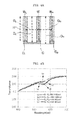
- FIG. 3A is a schematic cross-sectional view illustrating a structure of the wire grid layer used for Simulation 1.
- FIG. 3B is a graph depicting transmittance in Simulation 1.
- FIG. 4A is a schematic cross-sectional view illustrating a structure of the wire grid layer used for Simulation 2.
- FIG. 4B is a graph depicting transmittance in Simulation 2.
- the inorganic polarizing plate of the present invention contains at least a substrate, and a wire grid layer, and may further contain other members, such as a metal oxide layer, and a metal layer, as necessary.
- the wire grid layer contains a plurality of metal wires aligned on the substrate with gaps shorter than a wavelength of the light.
- the wire grid layer may be in contact with the substrate, or the metal oxide layer, or the meal layer may be provided between the wire grid layer and the substrate.
- a distance D L and a distance D R satisfy the following formula (1), where D L is a distance along a thickness direction of the substrate in a region R I between one metal wire W and a metal wire W L provided next to the metal wire W in the wire grid layer, and D R is a distance along the thickness direction of the substrate in a region R R between the metal wire W and a metal wire W R provided next to the metal wire W and at an opposite side to a side where the metal wire W L is provided.
- a gap G L and a gap G R satisfy the following formula (2), where G L is a gap between the metal wire W and the metal wire W L , and G R is a gap between the metal wire W and the metal wire W R .
- a ratio S L and a ratio S R satisfy the following formula (3), where S L is a ratio of the distance D L to the gap G L , and S R is a ratio of the distance D R to the gap G R .
- S L is a ratio of the distance D L to the gap G L
- S R is a ratio of the distance D R to the gap G R .
- the ratio S L is D L /G L
- the ratio S R is D R /G R .
- Rayleigh resonance caused by asymmetric two regions can be prevented by setting the ratio (S L ) and the ratio (S R ) of the two regions to the similar, i.e., satisfying the formula (3), even when the two regions present at both sides of the metal wire of the wire grid layer are asymmetric, i.e., the formulae (1) and (2) are satisfied.
- a reduction in the transmittance can be suppressed to 0.5% or less, when a relationship between the wavelength and the transmittance is measured. Note that, deterioration in transmittance properties due to the Rayleigh resonance caused by asymmetry can be sufficiently prevented, when the reduction in the transmittance is 0.5% or less.
- the prevention of the Rayleigh resonance can be achieved by adjusting the effective refractive indexes adjacent both sides of the metal wire to the similar degrees.
- the effective refractive index is an average refractive index of the medium in the region.
- the width of the metal wire, and gap of the metal wires in the wire grid layer for use in the present invention are sufficiently smaller than visible light, and sizes appropriately sufficiently applicable for the aforementioned mechanism.
- the effective refractive index can be associated with an electrostatic capacity between metal wires. Strictly, the effective refractive index is considered from an electromagnetic field distribution adjacent to the metal wire. In the present invention, however, the effective refractive index can be simplified as long as it is sufficient to attain an effect of reducing the Rayleigh resonance. Specifically, the effective refractive index can be considered to relate an amount determined by [distance (D)/gap (G)] of the region where the electromagnetic field spreads to a pseudo-capacity between the metal wires.
- the two regions are symmetric in view of the effective refractive index, if the amounts determined by [distance (D)/gap (G)] of the two regions are similar degrees.
- the effective refractive indexes adjacent to the metal wire in the regions both sides of the metal wire are similar degrees by satisfying the formula (3), to thereby prevent the Rayleigh resonance.
- the distance D L and the distance D R satisfy the following formula (1-2), and the gap G L and the gap G R satisfy the following formula (2-2), as a wider bandwidth of light can be polarized.
- the gap G L and the gap G R more preferably satisfy the following formula (2-3).
- 0 nm ⁇ ( D R ⁇ D L ) ⁇ 8 nm Formula (1-2) 0 nm ⁇
- the lower limit of the absolute value of a difference between the distance D L and the distance D R is appropriately selected depending on the intended purpose without any limitation, provided that it is greater than 0 nm.
- the lower limit thereof is preferably 1 nm or greater.
- the lower limit of the absolute value of a difference between the gap G L and the gap G R is appropriately selected depending on the intended purpose without any limitation, provided that it is greater than 0 nm.
- the lower limit thereof is preferably 1 nm or greater.
- the ratio S L of the distance D L to the gap G L and the ratio S R of the distance D R to the gap G R preferably satisfy the following formula (3-2). 1.00 ⁇ S R /S L ⁇ 1.30 Formula (3-2)
- a material, shape, and size of the metal wires are appropriately selected depending on the intended purpose without any limitation.
- Examples of the material of the metal wires include Al, and an Al alloy.
- Examples of the Al alloy include an AlSi alloy.
- the metal wires preferably contain Al or an AlSi alloy in view of optical properties, and easiness of a process.
- a shape of the metal wire is appropriately selected depending on the intended purpose without any limitation, and examples thereof include a rectangle, a trapezoid.
- a shape of the metal wire is a trapezoid
- a difference between two parallel bases is appropriately selected depending on the intended purpose without any limitation, but the difference is preferably greater than 0 nm, but 10 nm or less.
- the average width of the metal wires is appropriately selected depending on the intended purpose without any limitation, but the average width thereof is preferably 20 nm to 50 nm, more preferably 30 nm to 40 nm, in view of optical properties, and stability of a process.
- the average width of the metal wires can be determined, for example, by observing under a scanning electron microscope, or a transmission electron microscope. For example, widths of four metal wires are measured at arbitrary positions, and the average width is determined from the arithmetic mean of the measured values.
- the average gap between the metal wires is appropriately selected depending on the intended purpose without any limitation, but the average gap is preferably 80 nm to 200 nm, more preferably 100 nm to 140 nm, in view of easiness of a production, and stability.
- the average gap of the metal wires can be determined, for example, by observing under a scanning electron microscope, or a transmission electron microscope. For example, gaps between the metal wires are measured at arbitrary 4 positions, and the average gap is determined from the arithmetic mean of the measured values.
- the average thickness of the wire grid layer is appropriately selected depending on the intended purpose without any limitation, but the average thickness thereof is preferably 100 nm to 300 nm in view of optical properties.
- the average thickness of the wire grid layer is the average height of the metal wires.
- the average thickness is an arithmetic mean of a thickness of a layer in a cross-section cut the metal wire in a direction vertical to the length direction thereof.
- the average thickness can be determined by observing under a scanning electron microscope or a transmission electron microscope.
- thickness are measured at arbitrary 10 positions, and the average thickness is determined from the arithmetic mean of the measured values.
- the distance (D L ) may be referred to as “D L .” It is the same with the distance (D R ), the gap (G L ), the gap (G R ), the region (R L ), the region (R R ), and the height (H).
- the distance (D R ), the gap (G L ), the gap (G R ), the region (R L ), the region (R R ), and the height (H) of the metal wire are explained with reference to FIG. 1 , hereinafter.
- the inorganic polarizing plate of FIG. 1 contains a substrate 1 , a metal oxide layer 2 formed on the substrate 1 , and a wire grid layer 3 B formed on the metal oxide layer 2 .
- the wire grid layer 3 B is formed by aligning a plurality of metal wires.
- the height H of the metal wire W is a length from an edge (bottom edge) of the metal wire W at the side of the metal oxide layer 2 to the other edge (top edge) thereof.
- a metal wire W L is provided left next (in FIG. 1 ) to a metal wire W
- a metal wire W R is provided right next (in FIG. 1 ) to the metal wire W.
- the region R L is a region surrounded with the metal wire W, a metal wire W L , a virtual plane V L connecting a top of the metal wire W and a top of the metal wire W L , and the metal oxide layer 2 .
- the region R R is a region surrounded with the metal wire W, the metal wire W R , a virtual plane V R connecting a top of the metal wire W and a top of the metal wire W R , and the metal oxide layer 2 .
- the gap G L is the minimum distance between a centric position (relative to a height direction) on the center line C of the metal wire W in the width direction, and the center line C L of the metal wire W L in the width direction.
- the gap G R is the minimum distance between a centric position (relative to a height direction) on the center line C of the metal wire W in the width direction, and the center line C R of the metal wire W R in the width direction.
- the distance D R is a distance between the virtual plane V R , and the metal oxide layer 2 in the region R R .
- the distance D R is a distance measured to pass through a centric position between the metal wire W and the metal wire W R .
- the effective refractive index adjacent to the metal wire relates to a region where an electromagnetic field spreads. Therefore, the concave portion of the metal oxide layer 2 between the metal wires, which is included in a region where the electromagnetic field spreads, is also considered when the distance D L , and the distance D R are determined.
- the upper region of the metal wire (the upper region between the metal wire W and the metal wire W L , and the upper region between the metal wire W and the metal wire W R ) does not affect the ratio (S R /S L ). Therefore, the edge of the distance D L is determined as a virtual plane V L , and the edge of the distance D R is determined as a virtual plane V R .
- the light of a bandwidth for use is appropriately selected depending on the intended purpose without any limitation, and examples thereof include visible light.
- examples of the visible light include light in the range of 380 nm to 810 nm.
- Examples of the material of the substrate include glass, crystal, and ceramic. Among them, glass is preferable in view of a cost, and transmittance.
- the average thickness of the substrate is appropriately selected depending on the intended purpose without any limitation, but the average thickness thereof is preferably 300 ⁇ m to 1,000 ⁇ m.
- the metal oxide layer and the metal layer are provided, for example, between the substrate and the wire grid layer, or on a surface of the wire grid layer opposite to the side where the substrate is provided.
- the metal layer is a layer formed by forming a metal into a planar layer, and is different from the wire grid layer in that the metal layer is not in the form of a grid.
- the average thickness of the metal oxide layer is appropriately selected depending on the intended purpose without any limitation, but the average thickness thereof is preferably 20 nm to 50 nm in view of optical properties.
- the aforementioned other members are appropriately selected depending on the intended purpose without any limitation, and examples thereof include a protective layer, and a water-repellent layer.
- the protective layer can be provided, for example, in the area where the metal wires are not provided.
- a material of the protective layer is appropriately selected depending on the intended purpose without any limitation, and examples thereof include SiO 2 .
- the reliability of the inorganic polarizing plate can be provided by providing the protective layer therein.
- the water-repellent layer is provided, for example, on the protective layer.
- the water repellency of the inorganic polarizing plate is enhanced, and the reliability thereof can be improved by providing the water-repellent layer therein.
- a method for producing the inorganic polarizing plate is appropriately selected depending on the intended purpose without any limitation, but the following production method of an inorganic polarizing plate is preferable, as a wire grid layer having narrow pitches can be formed.
- the production method of an inorganic polarizing plate of the present invention contains at least a wire grid layer forming step, and may further contain other steps, as necessary.
- the wire grid layer forming step is appropriately selected depending on the intended purpose without any limitation, provided that it is a step containing forming a wire grid layer through double patterning using a coverage film.
- the wire grid layer forming step contains at least a metal layer forming process, a mask layer forming process, a resist pattern forming process, a coverage film forming process, a coverage film etching process, a resist ashing process, a mask layer etching process, a metal layer etching process, and a mask layer removing process, and may further contain other processes, such as an anti-reflection layer forming process, as necessary.
- the metal layer forming process is appropriately selected depending on the intended purpose without any limitation, provided that it is a process containing forming a metal layer on a substrate. Examples thereof include vacuum deposition.
- the metal layer is processed into a wire grid layer by the wire grid layer forming step.
- a material of the metal layer is appropriately selected depending on the intended purpose without any limitation, and examples thereof include Al, and an Al alloy. Examples of the Al alloy include an AlSi alloy.
- the metal oxide layer (e.g., a SiO 2 layer) may be formed on the substrate, on which the metal layer forming process is performed.
- the mask layer forming process is appropriately selected depending on the intended purpose without any limitation, provided that it is a process containing forming a mask layer on the metal layer. Examples thereof include vacuum deposition.
- a material of the mask layer is appropriately selected depending on the intended purpose without any limitation, and examples thereof include a multi-layer structure containing SiO 2 at least a part thereof.
- the resist pattern forming process is appropriately selected depending on the intended purpose without any limitation, provided that it is a process containing forming a resist pattern on the mask layer.
- the lines of the resist pattern have the similar width to that of the metal wire of the wire grid layer formed by the wire grid layer forming step, and the spaces of the resist pattern are each about twice the gap between two adjacent metal wires formed by the wire grid layer forming step.
- the coverage film forming process is appropriately selected depending on the intended purpose without any limitation, provided that it is a process containing forming a coverage film on the resist pattern formed by the resist pattern forming process, and the exposed mask layer between the resist pattern.
- the coverage film forming process is preferably atomic layer deposition, or chemical vapor deposition in view of coatability.
- the coverage film etching process is appropriately selected depending on the intended purpose without any limitation, provided that it is a process containing anisotropically etching the coverage film to expose the tops of the resist pattern and the mask layer, with remaining the coverage film on the side surfaces of the resist pattern.
- the coverage film etching process can be performed by dry etching.
- the resist ashing process is appropriately selected depending on the intended purpose without any limitation, provided that it is a process containing removing the resist pattern after the coverage film etching process.
- the resist ashing process can be performed with oxygen plasma.
- the mask layer etching process is appropriately selected depending on the intended purpose without any limitation, provided that it is a process containing etching the exposed mask layer after the resist ashing process, using the coverage film remained after the coverage film etching process as a mask.
- the mask layer etching process can be performed by dry etching.
- the metal layer etching process is appropriately selected depending on the intended purpose without any limitation, provided that it is a process containing etching the metal layer after the mask layer etching process, using the mask layer remained after the mask layer etching process, as a mask.
- the metal layer etching process can be performed by dry etching using a chlorine gas.
- the mask layer removing process is appropriately selected depending on the intended purpose without any limitation, provided that it is a process containing removing the mask layer remained after the metal layer etching process.
- the mask layer removing process can be performed by dry etching.
- Examples of the aforementioned other processes include an anti-reflection layer forming process.
- the anti-reflection layer forming process is appropriately selected depending on the intended purpose without any limitation, provided that it is a process, which is performed after the mask layer forming process but before the resist pattern forming process, and contains forming an anti-reflection layer on the mask layer.
- the anti-reflection layer forming process can be performed by spin coating.
- Reflections of exposure light on the metal layer can be prevented by forming the anti-reflection layer on the mask layer, at the time when resist pattern forming process is performed. Therefore, a desired resist pattern can be easily formed.
- FIGS. FIG. 2A to 2J One example of a method for producing the inorganic polarizing plate through double patterning using a coverage film is explained with reference to FIGS. FIG. 2A to 2J , hereinafter.
- FIGS. 2A to 2J are schematic cross-sectional views explaining one example of a step where a wire grid layer is formed through double patterning using a coverage film.
- a meal layer 3 is formed on a substrate 1 , to which a metal oxide layer 2 has been formed ( FIG. 2A ).
- a mask layer 4 is formed on the metal layer 3 ( FIG. 2B ).
- a resist film 5 is formed on the mask layer 4 ( FIG. 2C ).
- the resist film 5 is patterned by photolithography, to thereby form a resist pattern 5 A on the mask layer 4 ( FIG. 2D ).
- a coverage film 6 is formed on the resist pattern 5 A and the exposed mask layer 4 to correspond to the shapes thereof ( FIG. 2E ). Note that, the coverage film 6 is formed in a manner that space Sp, in which the coverage film 6 is not filled, is formed between the resist pattern 5 A.
- anisotropic etching is performed to selectively remove the coverage film 6 on the tops of the resist pattern 5 A and the mask layer 4 , to thereby obtain a coverage film pattern 6 A ( FIG. 2F ).
- resist ashing is performed to remove the resist pattern 5 A ( FIG. 2G ).
- resist ashing is performed to remove the resist pattern 5 A ( FIG. 2G ).
- only the coverage film pattern 6 A is remained on the mask layer 4 .
- etching is performed on the metal layer 3 using the mask layer pattern 4 A as a mask, to thereby obtain a metal wire 3 A ( FIG. 2I ).
- the wire grid layer is formed through double patterning using a coverage film.
- the region Ra and the region Rb illustrated in FIG. 2J have different environments when they are formed.
- the region Ra is a region formed based on the resist pattern 5 A
- the region Rb is a region formed based on a space Sp between the resist pattern when the coverage film 6 is formed. Therefore, heights (distance along the thickness direction of the substrate) and widths of the region Ra and the region Rb may be different because of the difference in the environment of each process in the wire grid layer forming step. For example, etching is performed even on the metal oxide layer 2 in the region Ra, and the region Rb, and the etching depth may be different.
- the regions present both sides of the metal wire 3 A may be asymmetric.
- the Rayleigh resonance may be caused by the aforementioned asymmetry.
- the inorganic polarizing plate can suppress the Rayleigh resonance, and prevents reduction in transmission properties.
- a change in the transmittance caused by varying a difference between the gap (G L ) and the gap (G R ) was confirmed. Specifically, a change in the transmittance was simulated by varying a gap between a metal wire (W) and a metal wire (W L ), and a gap between a metal wire (W) and a metal wire (W R ), which were formed of aluminium.
- FIG. 3A A schematic cross-sectional view of a structure of the wire grid layer used for the simulation is presented in FIG. 3A .
- the conditions and the transmittance dip (reduction in the transmittance) are presented below.
- FIG. 3B A graph depicting the transmittance by the simulation is presented in FIG. 3B .
- the difference between the gap (G R ) and the gap (G L ) was preferably 10 nm or less in order to make the reduction in the transmittance 0.5% or less.
- a change in the transmittance was confirmed by varying a difference between the gap (G L ) and the gap (G R ), with maintaining the distance (D L ) and the distance (D R ) to 8 mm.
- a change in the transmittance was simulated by forming a SiO 2 layer as an under layer below metal wires (W) and (W L ) formed of aluminium, making a distance (D L ) than a distance (D R ) by 8 nm, and varying a gap between the metal wires (W) and (W L ), and a gap between the metal wires (W) and (W R ).
- FIG. 4A A schematic cross-sectional view of a structure of the wire grid layer used for the simulation is presented in FIG. 4A .
- the conditions and the transmittance dip (reduction in the transmittance) are presented below.
- FIG. 4B A graph depicting the transmittance by the simulation is presented in FIG. 4B .
Landscapes
- Chemical & Material Sciences (AREA)
- Physics & Mathematics (AREA)
- Metallurgy (AREA)
- Engineering & Computer Science (AREA)
- Materials Engineering (AREA)
- Mechanical Engineering (AREA)
- Chemical Kinetics & Catalysis (AREA)
- Organic Chemistry (AREA)
- General Chemical & Material Sciences (AREA)
- General Physics & Mathematics (AREA)
- Optics & Photonics (AREA)
- Polarising Elements (AREA)
- Liquid Crystal (AREA)
Abstract
0 nm<(D R −D L) Formula (1);
0 nm<|G R −G L| Formula (2); and
0.90≤S R /S L≤1.30 Formula (3),
-
- where DL is distance along thickness direction of the substrate in region RL between one metal wire W and metal wire WL next to W in the wire grid layer, and DR is distance along the thickness direction of the substrate in region RR between W and metal wire WR provided next to W and at opposite side to side where WL is provided; GL is gap between W and WL, and GR is gap between W and WR; and SL is ratio of DL to GL, and SR is ratio of DR to GR.
Description
0 nm<(D R −D L) Formula (1);
0 nm<|G R −G L| Formula (2); and
0.90≤S R /S L≤1.30 Formula (3),
0 nm<(D R −D L)≤8 nm Formula (1-2); and
0 nm<|G R −G L|≤20 nm Formula (2-2).
<3> The inorganic polarizing plate according to <1> or <2>, wherein the substrate is glass.
<4> The inorganic polarizing plate according to any one of <1> to <3>, wherein the metal wire contains Al or an AlSi alloy.
<5> The inorganic polarizing plate according to any one of <1> to <4>, further containing a SiO2 layer between the substrate and the wire grid layer.
<6> A production method of an inorganic polarizing plate, containing:
0 nm<(D R −D L) Formula (1)
0 nm<|G R −G L| Formula (2)
0.90≤S R /S L≤1.30 Formula (3)
0 nm<(D R −D L)≤8 nm Formula (1-2)
0 nm<|G R −G L|≤20 nm Formula (2-2)
0 nm<|G R −G L|≤10 nm Formula (2-3)
The lower limit of the absolute value of a difference between the distance DL and the distance DR is appropriately selected depending on the intended purpose without any limitation, provided that it is greater than 0 nm. The lower limit thereof is preferably 1 nm or greater.
1.00≤S R /S L≤1.30 Formula (3-2)
| TABLE 1-1 | |||||
| Metal wire | Metal wire | Metal wire | |||
| (WL) | (W) | (WR) | |||
| Height (H) | 144 | 144 | 144 | ||
| (nm) | |||||
| Width | 35 | 35 | 35 | ||
| (nm) | |||||
| TABLE 1-2 | |||
| nm | |||
| Distance (DL) | 144 | ||
| Gap (GL) | Varied | ||
| Distance (DR) | 144 | ||
| Gap (GR) | Varied | ||
| TABLE 1-3 | ||||||
| Gap | Distance | SL | SR | Ratio | Transmittance | |
| (GL/GR) | (DL/DR) | (DL/GL) | (DR/GR) | SR/SL = S | dip | |
| (a) | 100 nm/ | 144 nm/ | 1.44 | 1.44 | 1.00 | 0.0% |
| 100 nm | 144 nm | |||||
| (b) | 100 nm/ | 144 nm/ | 1.44 | 1.60 | 1.11 | 0.5% |
| 90 nm | 144 nm | |||||
| (c) | 120 nm/ | 144 nm/ | 1.20 | 1.80 | 1.50 | 2.0% |
| 80 nm | 144 nm | |||||
| (d) | 130 nm/ | 144 nm/ | 1.11 | 2.06 | 1.86 | 4.1% |
| 70 nm | 144 nm | |||||
| TABLE 2-1 | |||||
| Metal wire | Metal wire | Metal wire | |||
| (WL) | (W) | (WR) | |||
| Height (H) | 144 | 144 | 144 | ||
| (nm) | |||||
| Width | 35 | 35 | 35 | ||
| (nm) | |||||
| TABLE 2-2 | |||
| nm | |||
| Distance (DL) | 152 | ||
| Gap (GL) | Varied | ||
| Distance (DR) | 160 | ||
| Gap (GR) | Varied | ||
| TABLE 2-3 | ||||||
| Gap | Distance | SL | SR | Ratio | Transmittance | |
| (GL/GR) | (DL/DR) | (DL/GL) | (DR/GR) | SR/SL = S | dip | |
| (a) | 90 nm/ | 152 nm/ | 1.69 | 1.45 | 0.86 | 1.1 |
| 110 nm | 160 nm | |||||
| (b) | 100 nm/ | 152 nm/ | 1.52 | 1.60 | 1.05 | 0.2 |
| 100 nm | 160 nm | |||||
| (c) | 110 nm/ | 152 nm/ | 1.38 | 1.78 | 1.29 | 0.2 |
| 90 nm | 160 nm | |||||
| (d) | 120 nm/ | 152 nm/ | 1.27 | 2.00 | 1.58 | 1.0 |
| 80 nm | 160 nm | |||||
Claims (10)
0 nm<(D R −D L) Formula (1)
0 nm<|G R −G L| Formula (2)
0.90≤S R /S L≤1.30 Formula (3)
0 nm<(D R −D L)≤8 nm Formula (1-2);and
0 nm<|G R −G L|≤20 nm Formula (2-2).
Applications Claiming Priority (2)
| Application Number | Priority Date | Filing Date | Title |
|---|---|---|---|
| JP2014101635A JP2015219319A (en) | 2014-05-15 | 2014-05-15 | Inorganic polarizer and method for manufacturing the same |
| JP2014-101635 | 2014-05-15 |
Publications (2)
| Publication Number | Publication Date |
|---|---|
| US20150331166A1 US20150331166A1 (en) | 2015-11-19 |
| US10295716B2 true US10295716B2 (en) | 2019-05-21 |
Family
ID=54538347
Family Applications (1)
| Application Number | Title | Priority Date | Filing Date |
|---|---|---|---|
| US14/709,862 Active US10295716B2 (en) | 2014-05-15 | 2015-05-12 | Inorganic polarizing plate and production method thereof |
Country Status (3)
| Country | Link |
|---|---|
| US (1) | US10295716B2 (en) |
| JP (1) | JP2015219319A (en) |
| CN (1) | CN105093380B (en) |
Families Citing this family (6)
| Publication number | Priority date | Publication date | Assignee | Title |
|---|---|---|---|---|
| KR102413970B1 (en) * | 2015-04-08 | 2022-06-28 | 삼성디스플레이 주식회사 | Wire grid polarizer and method for fabricating the same |
| JP2019061125A (en) * | 2017-09-27 | 2019-04-18 | デクセリアルズ株式会社 | Polarizing plate, method of manufacturing the same, and optical apparatus |
| CN108649140B (en) * | 2018-05-11 | 2019-09-20 | 武汉华星光电半导体显示技术有限公司 | OLED display panel and OLED display |
| JP2018189980A (en) * | 2018-07-19 | 2018-11-29 | デクセリアルズ株式会社 | Polarizing plate |
| JP7226936B2 (en) * | 2018-07-26 | 2023-02-21 | デクセリアルズ株式会社 | Polarizing plate and optical equipment |
| CN112218263B (en) * | 2019-07-12 | 2022-05-13 | 华为技术有限公司 | Data processing method, device and system |
Citations (15)
| Publication number | Priority date | Publication date | Assignee | Title |
|---|---|---|---|---|
| US6122103A (en) | 1999-06-22 | 2000-09-19 | Moxtech | Broadband wire grid polarizer for the visible spectrum |
| EP1775607A1 (en) | 2005-10-17 | 2007-04-18 | Asahi Kasei Kabushiki Kaisha | Wire grid polarizer and manufacturing method of the same |
| US20070242187A1 (en) | 2005-10-17 | 2007-10-18 | Hiroshi Yamaki | Wire grid polarizer and liquid crystal display device using the polarizer |
| JP2007310250A (en) | 2006-05-19 | 2007-11-29 | Hitachi Maxell Ltd | Method for manufacturing wire grid polarizer and wire grid polarizer |
| US20080055723A1 (en) | 2006-08-31 | 2008-03-06 | Eric Gardner | Durable, Inorganic, Absorptive, Ultra-Violet, Grid Polarizer |
| US20080278811A1 (en) | 2004-12-06 | 2008-11-13 | Perkins Raymond T | Selectively Absorptive Wire-Grid Polarizer |
| US20080316599A1 (en) | 2007-06-22 | 2008-12-25 | Bin Wang | Reflection-Repressed Wire-Grid Polarizer |
| US20100075503A1 (en) | 2008-09-19 | 2010-03-25 | Applied Materials, Inc. | Integral patterning of large features along with array using spacer mask patterning process flow |
| JP2010117646A (en) | 2008-11-14 | 2010-05-27 | Sony Corp | Functional grid structure and method of manufacturing the same |
| JP2010204626A (en) | 2009-02-05 | 2010-09-16 | Asahi Glass Co Ltd | Wire grid polarizer and manufacturing method therefor |
| US20110250757A1 (en) | 2010-04-09 | 2011-10-13 | Elpida Memory, Inc. | Method of manufacturing semiconductor device |
| JP2012080065A (en) | 2010-09-07 | 2012-04-19 | Sony Corp | Solid state image sensor, solid state image pickup device, image pickup equipment, and manufacturing method of polarization element |
| JP2012169408A (en) | 2011-02-14 | 2012-09-06 | Taiyo Nippon Sanso Corp | Material for mask, method for forming mask, method for forming pattern, and etching protection film |
| US20120250154A1 (en) * | 2010-09-21 | 2012-10-04 | Mark Alan Davis | Fine pitch wire grid polarizer |
| JP2012227130A (en) | 2011-04-07 | 2012-11-15 | Nissan Motor Co Ltd | Lamination device and lamination method |
Family Cites Families (8)
| Publication number | Priority date | Publication date | Assignee | Title |
|---|---|---|---|---|
| JP2006163291A (en) * | 2004-12-10 | 2006-06-22 | Canon Inc | Optical element and manufacturing method thereof |
| EP2023169A4 (en) * | 2006-04-07 | 2011-03-16 | Asahi Glass Co Ltd | WIRE GRID POLARIZER AND METHOD FOR PRODUCING THE SAME |
| JP4647545B2 (en) * | 2006-05-19 | 2011-03-09 | 日立マクセル株式会社 | Manufacturing method of wire grid polarizer |
| JP5933910B2 (en) * | 2006-08-15 | 2016-06-15 | ポラリゼーション ソリューションズ エルエルシー | Polarizer thin film and manufacturing method thereof |
| US8493658B2 (en) * | 2007-07-06 | 2013-07-23 | Semiconductor Energy Laboratory Co., Ltd. | Polarizer and display device including polarizer |
| JP5402317B2 (en) * | 2009-06-29 | 2014-01-29 | セイコーエプソン株式会社 | Polarizing element and manufacturing method of polarizing element, projection display device, liquid crystal device, and electronic apparatus |
| US8873144B2 (en) * | 2011-05-17 | 2014-10-28 | Moxtek, Inc. | Wire grid polarizer with multiple functionality sections |
| CN105572780B (en) * | 2016-02-03 | 2018-09-11 | 京东方科技集团股份有限公司 | Wire grid polarization device and preparation method thereof, display device |
-
2014
- 2014-05-15 JP JP2014101635A patent/JP2015219319A/en active Pending
-
2015
- 2015-05-12 US US14/709,862 patent/US10295716B2/en active Active
- 2015-05-15 CN CN201510251169.9A patent/CN105093380B/en active Active
Patent Citations (30)
| Publication number | Priority date | Publication date | Assignee | Title |
|---|---|---|---|---|
| US6122103A (en) | 1999-06-22 | 2000-09-19 | Moxtech | Broadband wire grid polarizer for the visible spectrum |
| JP2003502708A (en) | 1999-06-22 | 2003-01-21 | モックステック | Broadband wire grid polarizer for the visible spectrum |
| JP4800437B2 (en) | 1999-06-22 | 2011-10-26 | モックステック・インコーポレーテッド | Broadband wire grid polarizer for the visible spectrum |
| JP4763099B2 (en) | 1999-06-22 | 2011-08-31 | モックステック・インコーポレーテッド | Broadband wire grid polarizer for the visible spectrum |
| US20080278811A1 (en) | 2004-12-06 | 2008-11-13 | Perkins Raymond T | Selectively Absorptive Wire-Grid Polarizer |
| EP1775607A1 (en) | 2005-10-17 | 2007-04-18 | Asahi Kasei Kabushiki Kaisha | Wire grid polarizer and manufacturing method of the same |
| CN1952700A (en) | 2005-10-17 | 2007-04-25 | 旭化成株式会社 | Wire grid polarizer and manufacturing method of the same |
| US20070242187A1 (en) | 2005-10-17 | 2007-10-18 | Hiroshi Yamaki | Wire grid polarizer and liquid crystal display device using the polarizer |
| JP2008083657A (en) | 2005-10-17 | 2008-04-10 | Asahi Kasei Corp | Wire grid polarizer and liquid crystal display using the same |
| JP2007310250A (en) | 2006-05-19 | 2007-11-29 | Hitachi Maxell Ltd | Method for manufacturing wire grid polarizer and wire grid polarizer |
| US20080055723A1 (en) | 2006-08-31 | 2008-03-06 | Eric Gardner | Durable, Inorganic, Absorptive, Ultra-Violet, Grid Polarizer |
| JP2010530994A (en) | 2007-06-22 | 2010-09-16 | モックステック・インコーポレーテッド | Selective absorptive wire grid polarizer |
| JP2010530995A (en) | 2007-06-22 | 2010-09-16 | モックステック・インコーポレーテッド | Anti-reflection wire grid polarizer |
| JP2010531467A (en) | 2007-06-22 | 2010-09-24 | モックステック・インコーポレーテッド | Tolerant, inorganic and absorbing UV grid polarizer |
| US20080316599A1 (en) | 2007-06-22 | 2008-12-25 | Bin Wang | Reflection-Repressed Wire-Grid Polarizer |
| JP2010114424A (en) | 2008-09-19 | 2010-05-20 | Applied Materials Inc | Integral patterning of large feature portion and array using spacer mask patterning process flow |
| US20100075503A1 (en) | 2008-09-19 | 2010-03-25 | Applied Materials, Inc. | Integral patterning of large features along with array using spacer mask patterning process flow |
| JP2010117646A (en) | 2008-11-14 | 2010-05-27 | Sony Corp | Functional grid structure and method of manufacturing the same |
| JP2010204626A (en) | 2009-02-05 | 2010-09-16 | Asahi Glass Co Ltd | Wire grid polarizer and manufacturing method therefor |
| US20110286094A1 (en) | 2009-02-05 | 2011-11-24 | Asahi Glass Company, Limited | Wire-grid polarizer and process for producing the same |
| JP2011233878A (en) | 2010-04-09 | 2011-11-17 | Elpida Memory Inc | Method for manufacturing semiconductor device |
| US20110250757A1 (en) | 2010-04-09 | 2011-10-13 | Elpida Memory, Inc. | Method of manufacturing semiconductor device |
| JP2012080065A (en) | 2010-09-07 | 2012-04-19 | Sony Corp | Solid state image sensor, solid state image pickup device, image pickup equipment, and manufacturing method of polarization element |
| US20120319222A1 (en) | 2010-09-07 | 2012-12-20 | Sony Corporation | Solid-state imaging element, solid-state imaging device, imaging apparatus, and method of manufacturing polarizing element |
| US20120250154A1 (en) * | 2010-09-21 | 2012-10-04 | Mark Alan Davis | Fine pitch wire grid polarizer |
| US20140016197A1 (en) | 2010-09-21 | 2014-01-16 | Moxtek, Inc. | Fine Pitch Wire Grid Polarizer |
| JP2012169408A (en) | 2011-02-14 | 2012-09-06 | Taiyo Nippon Sanso Corp | Material for mask, method for forming mask, method for forming pattern, and etching protection film |
| JP2012227130A (en) | 2011-04-07 | 2012-11-15 | Nissan Motor Co Ltd | Lamination device and lamination method |
| US20140026398A1 (en) | 2011-04-07 | 2014-01-30 | Nissan Motor Co., Ltd. | Stacking device and stacking method |
| WO2013032570A1 (en) | 2011-09-02 | 2013-03-07 | Moxtek, Inc. | Fine pitch wire grid polarizer |
Non-Patent Citations (4)
| Title |
|---|
| Appeal Decision dated Jun. 5, 2018, by the Japanese Patent Office in corresponding Japanese Patent Application No. 2014-101635. (22 pages). |
| Notice of Reasons for Rejection issued by the Japanese Patent Office in corresponding Japanese Patent Application No. 2014-101635 dated Apr. 5, 2016 (6 pages including partial English translation). |
| Notice of Reasons for Rejection issued by the Japanese Patent Office in corresponding Japanese Patent Application No. 2014-101635 dated Aug. 2, 2016 (8 pages including partial English translation). |
| Office Action dated May 31, 2018, by the State Intellectual Property Office of People's Republic of China in corresponding Chinese Patent Application No. 201510251169.9 and an English Translation of the Office Action. (11 pages). |
Also Published As
| Publication number | Publication date |
|---|---|
| JP2015219319A (en) | 2015-12-07 |
| CN105093380A (en) | 2015-11-25 |
| CN105093380B (en) | 2020-02-07 |
| US20150331166A1 (en) | 2015-11-19 |
Similar Documents
| Publication | Publication Date | Title |
|---|---|---|
| US9988724B2 (en) | Inorganic polarizing plate having trapezoid shaped metal layers and production method thereof | |
| US10295716B2 (en) | Inorganic polarizing plate and production method thereof | |
| JP6117828B2 (en) | Inorganic polarizing plate | |
| US20210055591A1 (en) | Polarizer and optical apparatus | |
| US9097857B2 (en) | Polarizing plate and method for producing polarizing plate | |
| US9348076B2 (en) | Polarizer with variable inter-wire distance | |
| US10436964B2 (en) | Inorganic polarizing plate, method of manufacturing the same, and optical instrument | |
| KR101809313B1 (en) | Grid polarizing device and method for manufacturing grid polarizing device | |
| US8488070B2 (en) | Polarizing element and method for manufacturing the same, projection type display, liquid crystal device, and electronic apparatus | |
| US20180180785A1 (en) | Polarizing plate, method of manufacturing the same, and optical apparatus | |
| US20180180786A1 (en) | Polarizing plate, method of manufacturing the same, and optical apparatus | |
| US8913320B2 (en) | Wire grid polarizer with bordered sections | |
| JP2019536079A (en) | Embedded wire grid polarizer with high reflectivity on both sides | |
| JP6163180B2 (en) | Manufacturing method of polarizing plate | |
| EP2790043B1 (en) | Polarization separation element | |
| US10527768B2 (en) | Inorganic polarizing plate and method for manufacturing same | |
| US20190187350A1 (en) | Polarizing element | |
| US11867938B2 (en) | Polarizing plate having outermost layer of anti-reflection layer recessed towards substrate | |
| US20200371277A1 (en) | Polarizing plate, method of manufacturing the same, and optical apparatus | |
| CN110998384B (en) | Polarizing plate | |
| KR101836758B1 (en) | Grid polarizer and photo-alignment device | |
| US20210080634A1 (en) | Polarizing plate, polarizing plate manufacturing method, and optical apparatus | |
| US11644605B2 (en) | Polarizing element having alternately laminated dielectric layers and conductive layers and method for manufacturing polarizing element | |
| JP2025140405A (en) | Polarization element, manufacturing method of polarization element, and optical apparatus |
Legal Events
| Date | Code | Title | Description |
|---|---|---|---|
| AS | Assignment |
Owner name: DEXERIALS CORPORATION, JAPAN Free format text: ASSIGNMENT OF ASSIGNORS INTEREST;ASSIGNOR:HANASHIMA, NAOKI;REEL/FRAME:035618/0119 Effective date: 20150423 |
|
| STPP | Information on status: patent application and granting procedure in general |
Free format text: NOTICE OF ALLOWANCE MAILED -- APPLICATION RECEIVED IN OFFICE OF PUBLICATIONS |
|
| STPP | Information on status: patent application and granting procedure in general |
Free format text: PUBLICATIONS -- ISSUE FEE PAYMENT VERIFIED |
|
| STCF | Information on status: patent grant |
Free format text: PATENTED CASE |
|
| MAFP | Maintenance fee payment |
Free format text: PAYMENT OF MAINTENANCE FEE, 4TH YEAR, LARGE ENTITY (ORIGINAL EVENT CODE: M1551); ENTITY STATUS OF PATENT OWNER: LARGE ENTITY Year of fee payment: 4 |