US10291198B2 - Matching device and matching method - Google Patents
Matching device and matching method Download PDFInfo
- Publication number
- US10291198B2 US10291198B2 US15/553,334 US201615553334A US10291198B2 US 10291198 B2 US10291198 B2 US 10291198B2 US 201615553334 A US201615553334 A US 201615553334A US 10291198 B2 US10291198 B2 US 10291198B2
- Authority
- US
- United States
- Prior art keywords
- variable capacitance
- circle
- reflection coefficient
- capacitance
- capacitance capacitor
- Prior art date
- Legal status (The legal status is an assumption and is not a legal conclusion. Google has not performed a legal analysis and makes no representation as to the accuracy of the status listed.)
- Active, expires
Links
Images


Classifications
-
- H—ELECTRICITY
- H03—ELECTRONIC CIRCUITRY
- H03H—IMPEDANCE NETWORKS, e.g. RESONANT CIRCUITS; RESONATORS
- H03H7/00—Multiple-port networks comprising only passive electrical elements as network components
- H03H7/38—Impedance-matching networks
- H03H7/383—Impedance-matching networks comprising distributed impedance elements together with lumped impedance elements
-
- H—ELECTRICITY
- H01—ELECTRIC ELEMENTS
- H01J—ELECTRIC DISCHARGE TUBES OR DISCHARGE LAMPS
- H01J37/00—Discharge tubes with provision for introducing objects or material to be exposed to the discharge, e.g. for the purpose of examination or processing thereof
- H01J37/32—Gas-filled discharge tubes
- H01J37/32009—Arrangements for generation of plasma specially adapted for examination or treatment of objects, e.g. plasma sources
- H01J37/32082—Radio frequency generated discharge
- H01J37/32174—Circuits specially adapted for controlling the RF discharge
- H01J37/32183—Matching circuits
-
- H—ELECTRICITY
- H01—ELECTRIC ELEMENTS
- H01P—WAVEGUIDES; RESONATORS, LINES, OR OTHER DEVICES OF THE WAVEGUIDE TYPE
- H01P5/00—Coupling devices of the waveguide type
- H01P5/12—Coupling devices having more than two ports
- H01P5/16—Conjugate devices, i.e. devices having at least one port decoupled from one other port
- H01P5/18—Conjugate devices, i.e. devices having at least one port decoupled from one other port consisting of two coupled guides, e.g. directional couplers
-
- H—ELECTRICITY
- H03—ELECTRONIC CIRCUITRY
- H03H—IMPEDANCE NETWORKS, e.g. RESONANT CIRCUITS; RESONATORS
- H03H11/00—Networks using active elements
- H03H11/02—Multiple-port networks
- H03H11/28—Impedance matching networks
- H03H11/30—Automatic matching of source impedance to load impedance
-
- H—ELECTRICITY
- H03—ELECTRONIC CIRCUITRY
- H03H—IMPEDANCE NETWORKS, e.g. RESONANT CIRCUITS; RESONATORS
- H03H7/00—Multiple-port networks comprising only passive electrical elements as network components
- H03H7/38—Impedance-matching networks
- H03H7/40—Automatic matching of load impedance to source impedance
-
- H—ELECTRICITY
- H05—ELECTRIC TECHNIQUES NOT OTHERWISE PROVIDED FOR
- H05H—PLASMA TECHNIQUE; PRODUCTION OF ACCELERATED ELECTRICALLY-CHARGED PARTICLES OR OF NEUTRONS; PRODUCTION OR ACCELERATION OF NEUTRAL MOLECULAR OR ATOMIC BEAMS
- H05H1/00—Generating plasma; Handling plasma
- H05H1/24—Generating plasma
- H05H1/46—Generating plasma using applied electromagnetic fields, e.g. high frequency or microwave energy
-
- H05H2001/4682—
-
- H—ELECTRICITY
- H05—ELECTRIC TECHNIQUES NOT OTHERWISE PROVIDED FOR
- H05H—PLASMA TECHNIQUE; PRODUCTION OF ACCELERATED ELECTRICALLY-CHARGED PARTICLES OR OF NEUTRONS; PRODUCTION OR ACCELERATION OF NEUTRAL MOLECULAR OR ATOMIC BEAMS
- H05H2242/00—Auxiliary systems
- H05H2242/20—Power circuits
- H05H2242/26—Matching networks
Definitions
- the present invention relates to a matching device for matching an output of a RF (Radio Frequency) generator and a load.
- RF Radio Frequency
- a plasma processing apparatus is used in a semiconductor manufacturing process for performing etching or thin film formation.
- a power supply source of the plasma processing apparatus a RF generator is used.
- a matching device is interposed, as a unit for matching an impedance, between the RF generator and the plasma processing apparatus as described in, e.g., Patent Document 1.
- FIG. 7 is a functional block diagram of a conventional matching device 100 .
- the matching device 100 is interposed between a RF generator 2 and a plasma processing apparatus 3 .
- a plasma is generated by the plasma processing apparatus 3 by supplying a high frequency power outputted from the RF generator 2 to the plasma processing apparatus 3 through the matching device 100 .
- An output impedance of the RF generator 2 is generally 50 ⁇ . Therefore, it is preferable to set an input impedance of the matching device 100 to 50 ⁇ by converting an input impedance of the plasma processing apparatus 3 using the matching device 100 .
- the input impedance of the plasma processing apparatus 3 varies depending on types, flow rates, pressures and temperatures of gases to be supplied to the plasma processing apparatus 3 . Therefore, the matching device 100 needs to perform adaptive matching in response to the temporally varying input impedance of the plasma processing apparatus 3 .
- the matching device 100 shown in FIG. 7 includes a directional coupler 11 for detecting a travelling wave and a reflected wave, a matching circuit 30 having a matching element for matching an impedance between the RF generator 2 and the plasma processing apparatus 3 , and a control unit 120 for controlling a circuit constant of the matching element of the matching circuit 30 .
- a high frequency power (travelling wave: Pf) travelling from an RF in terminal toward an RF out terminal is detected by the directional coupler 11 and outputted to a FORWARD terminal.
- a high frequency power (reflected wave: Pr) travelling from the RF out terminal toward the RF in terminal is detected by the directional coupler 11 and outputted to a REFLECT terminal.
- the high frequency power Pf travelling from the RF in terminal toward the RF out terminal is not detected at the REFLECT terminal, or even if detected, the amount thereof is very small.
- the high frequency power Pr travelling from the RF out terminal toward the RF in terminal is not detected at the FORWARD terminal, or even if detected, the amount thereof is very small.
- a reflection coefficient ⁇ is defined from an amplitude ratio r of the reflected wave Pr to the travelling wave Pf and a phase difference ⁇ therebetween, as in the following Eq. (1).
- ⁇ r ⁇ exp( j ⁇ )( j : imaginary unit) Eq. (1)
- the reflection coefficient calculation unit 21 calculates the reflection coefficient ⁇ by obtaining the amplitude ratio r and the phase difference ⁇ based on the travelling wave Pf and the reflected wave Pr. Specifically, the travelling wave Pf and the reflected wave Pr are transformed to a frequency domain by FFT (Fast Fourier Transform), and the amplitude ratio r and the phase difference ⁇ are calculated by comparing the amplitudes and the phases of the travelling wave Pf and the reflected wave Pr at a frequency equal to that of the high frequency power outputted from the RF generator 2 .
- FFT Fast Fourier Transform
- a capacitance calculation unit 122 calculates a capacitance of a capacitor which makes the reflection coefficient ⁇ close to zero based on the reflection coefficient ⁇ calculated by the reflection coefficient calculation unit 21 . The calculation of the capacitance of the capacitor will be described later.
- a capacitance setting unit 23 sets and changes a capacitance of a variable capacitance capacitor in the matching circuit 30 based on the capacitance of the capacitor which is calculated by the capacitance calculation unit 122 .
- FIG. 2 is a block diagram of the matching circuit 30 .
- a circuit configuration of the matching circuit 30 is determined by a variation range of the input impedance of the plasma processing apparatus 3 which acts as a load. In that case, a ⁇ -type matching circuit will be described as an example.
- the matching circuit 30 includes variable capacitance capacitors 31 and 32 , an inductance 33 , and transmission lines 35 and 36 .
- the transmission lines 35 and 36 may be configured as coaxial cables, metal plates or the like and may include a lumped constant circuit of an inductor or a capacitor.
- An input terminal 30 a of the matching circuit 30 and one end of the variable capacitance capacitor 31 are connected through the transmission line 35 . The other end of the variable capacitance capacitor 31 is grounded.
- An output terminal 30 b of the matching circuit 30 and one end of the variable capacitance capacitor 32 are connected through the transmission line 36 . The other end of the variable capacitance capacitor 32 is grounded.
- the variable capacitance capacitors 31 and 32 and the inductance 33 serve as matching elements for matching an impedance between the RF generator 2 and the plasma processing apparatus 3 .
- the matching circuit 30 further includes a variable capacitance capacitor control terminal 31 a for controlling a capacitance of the variable capacitance capacitor 31 and a variable capacitance capacitor control terminal 32 a for controlling a capacitance of the variable capacitance capacitor 32 .
- variable capacitance capacitor of the matching circuit is controlled such that the reflection coefficient ⁇ calculated from the travelling wave Pf and the reflected wave Pr detected by the directional coupler 11 becomes close to zero.
- the variable capacitance at this time is calculated by the following Eqs. (2) and (3).
- VC 1 indicates a capacitance of the variable capacitance capacitor 31 .
- VC 2 indicates a capacitance of the variable capacitance capacitor 32 .
- VC1( n ) VC1( n ⁇ 1)+real( ⁇ ( n ))* S 1 Eq. (2)
- VC2( n ) VC2( n ⁇ 1) ⁇ imag( ⁇ ( n ))* S 2 Eq. (3)
- real( ) indicates a real part of a complex number in parentheses
- imag( ) indicates an imaginary part of a complex number in parentheses
- S 1 and S 2 indicate coefficient and determine an update amount of the capacitance of the capacitor.
- the above Eq. (2) is used for updating VC 1 .
- the above Eq. (3) is used for updating VC 2 .
- VC 1 (n) is calculated by adding a value obtained by multiplying the real part of the reflection coefficient ⁇ by the coefficient S 1 to a previously updated VC 1 (n ⁇ 1).
- VC 2 (n) is calculated by subtracting a value obtained by multiplying the imaginary part of the reflection coefficient ⁇ by the coefficient S 2 from a previously updated VC 2 (n ⁇ 1).
- whether the update amount (real( ⁇ )*S 1 or imag( ⁇ )*S 2 ) is added or subtracted depends on the circuit type of the matching circuit 30 and the input impedance of the load to be matched.
- the algorithm of such a conventional technique is disadvantageous in that VC 1 and VC 2 do not converge on a matching point when the load impedance changes.
- the impedance of the plasma load changes.
- the impedance of the plasma load changes abruptly before and after the ignition of the plasma and also changes depending on types, flow rates, pressures and temperatures of gases to be supplied to the plasma processing apparatus.
- VC 1 and VC 2 for allowing the input impedance of the matching circuit 30 to be matched to 50 ⁇ are determined by the load impedance connected to the output of the matching device 100 . Since, however, the plasma load changes, VC 1 and VC 2 for the matching also change. Therefore, in the case of using the algorithm of the above Eqs. (2) and (3), VC 1 and VC 2 may not converge on the matching point. This is because VC 1 is calculated by the above Eq. (2) and VC 2 is calculated by the above Eq. (3). In other words, VC 1 is calculated from the real part of the reflection coefficient and VC 2 is calculated from the imaginary part of the reflection coefficient. However, the relations in the above Eqs. (2) and (3) may not be satisfied depending on the impedance of the plasma load or the capacitance of the variable capacitance capacitor. In that case, VC 1 and VC 2 do not converge on the matching point.
- the present invention provides a matching algorithm that converges on a matching point regardless of the load impedance.
- the matching device includes: a directional coupler configured to detect a travelling wave and a reflected wave; a matching circuit including an input terminal, an output terminal, a first variable capacitance capacitor having one end connected to the input terminal through a first transmission line and the other end that is grounded, a second variable capacitance capacitor having one end connected to the output terminal through a second transmission line and the other end that is grounded, and an inductance having one end connected to said one end of the first variable capacitance capacitor and the other end connected to said one end of the second variable capacitance capacitor; and a control unit configured to control a capacitance value of the first variable capacitance capacitor and a capacitance value of the second variable capacitance capacitor based on the travelling wave and the reflected wave detected by the directional coupler.
- the control unit calculates a reflection coefficient based on the travelling wave and the reflected wave detected by the directional coupler, changes the capacitance of the second variable capacitance capacitor such that the capacitance of the second variable capacitance capacitor goes to a circle described by a trace of the reflection coefficient which passes through a matching point on a Smith chart, calculates and predicts an intersection point with the circle, and determines a direction of fine-tuning of the capacitance of the first variable capacitance capacitor based on the predicted intersection point (expected point on circumference).
- the control unit fine-tunes the capacitance of the first variable capacitance capacitor such that the capacitance of the first variable capacitance capacitor is increased when an imaginary part of the expected point on circumference is negative and fine-tunes the capacitance of the first variable capacitance capacitor such that the capacitance of the first variable capacitance capacitor is decreased when the imaginary part of the expected point on circumference is positive.
- the control unit changes the capacitance of the first variable capacitance capacitor such that the calculated reflection coefficient becomes close to zero when a distance between the calculated reflection coefficient and the circle becomes a predetermined value or less.
- the control unit fine-tunes the capacitance of the second variable capacitance capacitor such that the capacitance of the second variable capacitance capacitor is decreased in the case of outward deviation from the circle and fine-tunes the capacitance of the second variable capacitance capacitor such that the capacitance of the second variable capacitance capacitor is increased in the case of inward deviation from the circle.
- the matching algorithm of the preset invention can converge on the matching point regardless of the load impedance.
- FIG. 1 is a block diagram of a matching device according to a first embodiment.
- FIG. 2 is a block diagram of a matching circuit according to the first embodiment.
- FIG. 3 explains an example of a reflection coefficient trace in the case of changing a capacitance of a variable capacitance capacitor.
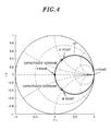
- FIG. 4 explains another example of the reflection coefficient trace in the case of changing a capacitance of a variable capacitance capacitor.
- FIG. 5 shows a reflection coefficient trace according to the first embodiment.
- FIG. 6 is a flowchart of an impedance matching process according to the first embodiment.
- FIG. 7 is a block diagram of a conventional matching device.
- FIGS. 8A to 8C explain circle matching.
- FIG. 9 is a block diagram of a matching device according to a second embodiment.
- FIG. 10 is a flowchart of an impedance matching process according to the second embodiment.
- FIG. 11 shows a reflection coefficient trace according to the second embodiment.
- FIG. 12 explains predictive control in a first example of the second embodiment.
- FIGS. 13 to 15 explain predictive control in a second example of the second embodiment.
- FIG. 1 is a block diagram of a matching device 10 according to the first embodiment.
- Like reference numerals used in FIGS. 1 and 7 designate like parts, and redundant description thereof will be omitted.
- the matching device 10 includes a directional coupler 11 for detecting a travelling wave and a reflected wave, a matching circuit 30 having a matching element for matching an impedance between a RF generator 2 and a plasma processing apparatus 3 , a control unit 20 for controlling a circuit constant of the matching element of the matching device 10 , and a storage unit 25 .
- the matching circuit 30 includes the input terminal 30 a , the output terminal 30 b , the first variable capacitance capacitor 31 having one end connected to the input terminal 30 a through the transmission line 35 and the other end that is grounded, the second variable capacitance capacitor 32 having one end connected to the output terminal 30 b through the transmission line 36 and the other end that is grounded, and the inductance 33 having one end connected to the one end of the first variable capacitance capacitor 31 and the other end connected to the one end of the second variable capacitance capacitor 32 .
- the control unit 20 includes the reflection coefficient calculation unit 21 , the capacitance calculation unit 22 , and the capacitance setting unit 23 . As described above, the control unit 20 calculates a reflection coefficient based on the travelling wave and the reflected wave detected by the directional coupler 11 and controls a capacitance value of the first variable capacitance capacitor 31 and a capacitance value of the second variable capacitance capacitor 32 by using the calculated reflection coefficient.
- the storage unit 25 stores information on a circle or the like which will be described later.
- the matching device 10 is different from the conventional matching device 100 in the processing of the capacitance calculation unit 22 , i.e., the control of the capacitance value VC 1 of the variable capacitance capacitor 31 and the capacitance value VC 2 of the variable capacitance capacitor 32 of the matching circuit 30 . Further, the matching device 10 is different from the conventional matching device 100 in that the storage unit 25 for storing information on a circle is provided. The other configurations are the same as those of the conventional matching device 100 .
- the information on a circle is the information on a position or a size of a circle described by a trace of the reflection coefficient ⁇ which passes through a matching point (where the real part and the imaginary part of the reflection coefficient ⁇ are zero) on a Smith chart. It is known that the information on a circle is determined based on conditions of the transmission line 35 , i.e., a characteristic impedance Z L and a line length L of the transmission line 35 .
- the capacitance calculation unit 22 calculates the capacitance values VC 1 and VC 2 of the variable capacitance capacitors 31 and 32 of the matching circuit 30 which correspond to the calculated reflection coefficient ⁇ based on the information on a circle which is stored in the storage unit 25 and the reflection coefficient ⁇ calculated by the reflection coefficient calculation unit 21 . In other words, the capacitance calculation unit 22 calculates the capacitance values VC 1 and VC 2 that make the reflection coefficient ⁇ smaller.
- the capacitance calculation unit 22 calculates the capacitance value VC 2 of the variable capacitance capacitor 32 of the matching circuit 30 such that the reflection coefficient ⁇ calculated by the reflection coefficient calculation unit 21 becomes close to the circle stored in the storage unit 25 .
- the capacitance setting unit 23 changes the capacitance value VC 2 of the variable capacitance capacitor 32 to the calculated capacitance value. Accordingly, the reflection coefficient ⁇ is positioned on the circle by the capacitance setting unit 23 .
- the capacitance calculation unit 22 calculates the capacitance value VC 1 of the variable capacitance capacitor 31 of the matching circuit 30 such that the reflection coefficient ⁇ calculated by the reflection coefficient calculation unit 21 becomes smaller.
- the capacitance setting unit 23 changes the capacitance value VC 1 of the variable capacitance capacitor 31 to the calculated capacitance value. Accordingly, the reflection coefficient ⁇ is positioned on the matching point (where the reflection coefficient ⁇ is zero) by the capacitance setting unit 23 .
- the information on a circle determined by the transmission line 35 has been previously stored in the storage unit 25 .
- the information on a circle is determined based on the condition of the transmission line 35 , i.e., the characteristic impedance Z L and the line length L of the transmission line 35 .
- the transmission line 35 is short enough to be ignored, a circle R 1 shown in FIG. 3 to be described later is drawn.
- a circle R 2 shown in FIG. 4 or a circle R 3 shown in FIG. 5 which will be described later is drawn.
- the values of VC 1 and VC 2 are set to X and Y, respectively.
- a trace of the input impedance of the matching circuit 30 i.e., the trace of the reflection coefficient ⁇ , in the case of changing the value of VC 1 from the matching condition in which VC 1 is X and VC 2 is Y, is shown on the Smith chart of FIG. 3 .
- the transmission line 35 is short enough to be ignored compared to the wavelength ⁇ of the travelling wave and the reflected wave.
- the trace of the reflection coefficient ⁇ describes the circle R 1 having as a diameter a segment connecting G point and F point where the matching is realized.
- the reflection coefficient ⁇ at the F point has an imaginary part ( ⁇ i) of zero and a real part ( ⁇ i) of zero (the input impedance of the matching device 10 is 50 ⁇ ).
- the reflection coefficient ⁇ at the G point has an imaginary part of zero and a real part of ⁇ 1.
- FIG. 3 shows the case in which the transmission line 35 may be ignored. However, the transmission line 35 may not be ignored actually.
- FIG. 4 shows a trace of the reflection coefficient ⁇ on the Smith chart which is obtained when the transmission line 35 has a characteristic impedance of 50 ⁇ and a line length of ⁇ /4.
- the trace of the reflection coefficient ⁇ draws a circle R 2 having as a diameter a segment connecting H point and the F point where the matching is realized.
- the reflection coefficient ⁇ at the H point has an imaginary part of zero and a real part of 1 (the input impedance of the matching device 10 is infinite).
- Z 1 indicates an input impedance in the case where the transmission line 35 may be ignored ( FIG. 3 )
- Z 2 indicates an input impedance in the case where the transmission line 35 may not be ignored ( FIG. 4 ).
- the circle R 1 shown in FIG. 3 is changed to the circle R 2 shown in FIG. 4 .
- Z 2 Z L ⁇ Z 1 + jZ L ⁇ tan ⁇ ( 2 ⁇ ⁇ ⁇ ⁇ ⁇ L ) Z L + jZ 1 ⁇ tan ⁇ ( 2 ⁇ ⁇ ⁇ ⁇ ⁇ L ) Eq . ⁇ ( 4 )
- FIG. 5 shows a trace of the reflection coefficient ⁇ on the Smith chart in the case of performing the impedance matching according to the embodiment by the matching circuit 30 under the condition that the transmission line 35 has a characteristic impedance of 50 ⁇ and a line length of ⁇ /4 as in the case shown in FIG. 4 .
- C point is the reflection coefficient ⁇ , i.e., the input impedance of the matching device 10 , at the time when VC 1 and VC 2 are initial values (e.g., minimum value of the variable capacitance capacitor), in the case where the plasma load has a certain input impedance.
- the control unit 20 increases only VC 2 until the reflection coefficient ⁇ reaches from the C point where VC 1 and VC 2 are the initial values to D point on the circle R 3 .
- the circle R 3 is the same as the circle R 2 shown in FIG. 4 .
- the information on the circle R 3 is stored in the storage unit 25 .
- VC 2 becomes a matching capacitance Y.
- VC 1 remains at the initial value. Therefore, the control unit 20 gradually increases VC 1 .
- VC 1 is increased, the reflection coefficient ⁇ moves on the circle R 3 as described above. Accordingly, it is preferable to stop the increase of VC 1 when the reflection coefficient ⁇ becomes zero. At this time, VC 1 becomes a matching capacitance X.
- the trace shown in FIG. 5 is an example of the case in which an input impedance of the plasma load is a certain value.
- the positions of the C point and the D point are changed.
- the reflection coefficient ⁇ is positioned on the circle R 3 .
- a minimum value of the variable capacitance capacitor is selected as the initial values of VC 1 and VC 2 .
- a maximum value of the variable capacitance capacitor or another value may be selected. In that case, the position of the C point is changed.
- the reflection coefficient ⁇ moves on the circle R 3 .
- the control unit 20 controls only VC 2 until the reflection coefficient ⁇ is positioned on the circle R 3 and then controls only VC 1 after the reflection coefficient ⁇ is positioned on the circle R 3 .
- the reflection coefficient ⁇ is outside the circle R 3 if VC 2 is greater than the matching value Y and, thus, VC 2 is decreased so that the reflection coefficient ⁇ is positioned on the circle R 3 .
- the reflection coefficient ⁇ is inside the circle R 3 if VC 2 is smaller than the matching value Y and, thus, VC 2 is increased so that the reflection coefficient ⁇ is positioned on the circle R 3 .
- VC 1 is controlled in the following manner. Specifically, when the imaginary part of the reflection coefficient ⁇ is positive, VC 1 is greater than the matching value X and, thus, VC 1 is decreased so that the reflection coefficient ⁇ becomes zero. On the contrary, when the imaginary part of the reflection coefficient ⁇ is negative, VC 1 is smaller than the matching value X and, thus, VC 1 is increased so that the reflection coefficient ⁇ becomes zero.
- VC 2 and VC 1 are controlled as described above.
- VC 2 is controlled so that the reflection coefficient ⁇ is positioned on the circle R 3 and, then, VC 1 is controlled.
- FIGS. 4 and 5 show as an example the case in which the transmission line 35 has a characteristic impedance of 50 ⁇ and a line length of ⁇ /4 in the matching circuit 30 of FIG. 2 .
- the present invention is not limited thereto. If the condition of the transmission line 35 is different from the above condition, the trace of the circle in the case of changing VC 1 under the condition in which VC 2 is the matching capacitance is different from the trace of the circle R 3 shown in FIGS. 4 and 5 . Therefore, the trace of the circle which satisfies the condition of the transmission line 35 may be set by the above-described Eq. (4).
- FIG. 6 is a flowchart of an impedance matching process according to the first embodiment. This process is performed by the control unit 20 .
- the information on the circle shown in FIGS. 4 and 5 (size and position on the Smith chart) is stored in the storage unit 25 (step S 1 of FIG. 6 ). Since the information on the circle is determined depending on the transmission line 35 as described above, the information corresponding to the matching circuit 30 is required.
- the initial values of VC 1 and VC 2 are also set.
- the reflection coefficient ⁇ at that time is calculated from the travelling wave Pf and the reflected wave Pr detected by the directional coupler 11 (step S 2 ). Then, an absolute value of the reflection coefficient ⁇ and a predetermined value L are compared (step S 3 ). When the absolute value of the reflection coefficient ⁇ is smaller than or equal to L (Yes in step S 3 ), the process returns to the step S 2 to obtain the travelling wave Pf and the reflected wave Pr from the directional coupler 11 and calculate again the reflection coefficient ⁇ at that time.
- the predetermined value L is a threshold value for determining whether or not the matching is realized.
- the predetermined value L is ideally zero. However, a certain threshold value L is used because it is actually difficult to make the reflection coefficient ⁇ zero.
- the predetermined value L is determined by a reflection-resistant power of the RF generator 2 and specifications of the plasma processing apparatus 1 using the RF generator 2 .
- step S 4 in order to determine whether or not the reflection coefficient ⁇ is positioned on the circle defined by the initial setting (step S 1 ), the information on the circle is acquired from the storage unit 25 and a minimum value P of the distance between the reflection coefficient ⁇ and the circle is calculated.
- a predetermined threshold value M (Yes in step S 5 )
- VC 2 is not the matching value and thus is controlled to be changed.
- the predetermined threshold value M is ideally zero. Since, however, it is actually difficult to set the predetermined threshold value M to zero, the predetermined threshold value M is set to a certain value.
- VC 2 is the matching value and there is no need to change VC 2 . Therefore, the process proceeds to an operation of controlling VC 1 (i.e., the capacitance of the variable capacitance capacitor 31 ). In other words, it is determined that the reflection coefficient ⁇ is positioned on the circle and the process proceeds to a step S 10 .
- step S 6 it is determined whether or not the reflection coefficient ⁇ is inside the circle to decide whether to increase or decrease VC 2 (i.e., the capacitance of the variable capacitance capacitor 32 ).
- VC 2 is smaller than Y and thus is increased (step S 7 ).
- step S 8 VC 2 is greater than Y and thus is decreased (step S 8 ).
- the amount of increase and decrease may be set in advance.
- the minimum value P can be smaller than or equal to the predetermined threshold value M.
- the reflection coefficient ⁇ can be positioned substantially on the circle.
- step S 10 it is determined whether or not the imaginary part of the reflection coefficient ⁇ is negative. In other words, it is determined whether or not VC 1 is smaller than X. As described above, when the imaginary part of the reflection coefficient ⁇ is negative, VC 1 is smaller than X. When the imaginary part of the reflection coefficient ⁇ is positive, VC 1 is greater than X. Therefore, when the imaginary part of the reflection coefficient ⁇ is negative (Yes in step S 10 ), VC 1 is increased. When the imaginary part of the reflection coefficient ⁇ is positive (No in step S 10 ), VC 1 is decreased. By changing VC 1 in the above manner, the reflection coefficient ⁇ becomes close to zero. The amount of increase and decrease may be set in advance.
- the control unit 20 calculates the reflection coefficient based on the travelling wave and the reflected wave detected by the directional coupler 11 .
- the control unit 20 changes the capacitance value of the second variable capacitance capacitor 32 and the calculated reflection coefficient to make the distance equal to or less than the predetermined value.
- the control unit 20 changes the capacitance value of the first variable capacitance capacitor 31 and makes the calculated reflection coefficient smaller without changing the distance.
- the present embodiment has at least the following effects.
- the capacitance value of the first variable capacitance capacitor is changed and the calculated reflection coefficient is decreased. Accordingly, the matching algorithm of the present invention can converge on the matching point regardless of the load impedance.
- U indicates a real part of the reflection coefficient ⁇
- V indicates an imaginary part of the reflection coefficient ⁇ .
- FIGS. 8A to 8C show graphs in which a plurality of fixed values of VC 1 is plotted while varying VC 2 .
- the basic operation of the circle matching may cause the following problems.
- the circle R 4 may not be a complete circle depending on a load condition.
- a matching device provides a technique for adapting circle matching to a dynamic load as a solution to the above drawbacks (1) to (3).
- a configuration of the matching device according to the second embodiment will be described with reference to FIG. 9 .
- a matching device 10 A according to the second embodiment is different from the matching device 10 of the first embodiment in the processing of the capacitance calculation unit 22 , i.e., the control of the capacitance VC 1 of the variable capacitance capacitor 31 of the matching circuit 30 and the capacitance VC 2 of the variable capacitance capacitor 32 of the matching circuit 30 .
- the other configurations of the matching device 10 A of the second embodiment are the same as those of the matching device 10 of the first embodiment.
- the capacitance calculation unit 22 A of the matching device 10 A of the second embodiment has following features in addition to the features of the capacitance calculation unit 22 of the first embodiment.
- a circle in circle matching is specified and a hysteresis is provided at IN/OUT of a circumference region to prevent hunting.
- the VC 2 control is predictive control for calculating an intersection point with the circle (circumference), not a simple operation of determining a direction.
- VC 2 and VC 1 are controlled by determining the direction of fine-tuning of VC 1 based on the intersection point with the circumference (expected point on circumference) which is predicted by the predictive control.
- the matching by VC 1 (movement toward the target point on the circumference) and the fine-tuning of VC 2 are performed at the same time to prevent deviation from the circumference region.
- the direction of the fine-tuning of VC 2 is a decreased direction in the case of outward deviation from the circle and an increased direction in the case of inward deviation from the circle.
- FIG. 10 is a flowchart of the impedance matching process according to the second embodiment.
- FIG. 11 shows a trace of a reflection coefficient according to the second embodiment.
- the impedance matching process shown in FIG. 10 is performed by the capacitance calculation unit 22 A.
- the respective steps will be described.
- VC 2 is changed such that VC 2 goes to a circle R from the reflection coefficient ⁇ , i.e., the input impedance of the matching device 10 , at the time when VC 1 and VC 2 are initial values.
- ⁇ the reflection coefficient
- VC 1 and VC 2 are initial values.
- an intersection point with the circle R is predicted by calculation and a direction of fine-tuning of VC 1 is determined based on the predicted intersection point.
- VC 1 is fine-tuned in the determined direction.
- a V coordinate of the predicted intersection point is negative, VC 1 is fine-tuned to be increased.
- VC 1 is fine-tuned to be decreased.
- the circumference region is a region between a circumference of an inner circle Rin of the circle R and a circumference of an outer circle Rout of the circle R. It is determined whether or not the reflection coefficient ⁇ is positioned within the circumference region (within a predetermined distance from the circle R). When the reflection coefficient ⁇ is positioned within the circumference region (Yes), the process proceeds to a step S 26 . When the reflection coefficient ⁇ is not positioned within the circumference region (No), the process proceeds to the step S 21 .
- the reflection coefficient ⁇ may be changed by the load variation.
- the process proceeds to the step S 21 .
- the process proceeds to a step S 25 .
- VC 2 is returned to a direction of the immediately previous VC 2 .
- the process proceeds to a step S 28 .
- the process proceeds to a step S 27 .
- Step S 27 Determining Whether or not the Reflection Coefficient is Positioned within a Target Region
- the target region is close to the matching point and greater than the circumference region near the matching point. It is determined whether or not the reflection coefficient ⁇ is positioned inside the target region. When the reflection coefficient ⁇ is positioned within the target region (Yes), the process proceeds to a step S 28 . When the reflection coefficient ⁇ is not positioned within the target region (No), the process proceeds to the step S 21 .
- the fine-tuning of VC 2 is also performed to prevent the deviation from the circumference region.
- the direction of the fine-tuning of VC 2 may be determined uniquely. Specifically, the direction of the fine-tuning of VC 2 is a decreased direction in the case of outward deviation from the circle and an increased direction in the case of inward deviation from the circle.
- the reflection coefficient ⁇ It is determined whether or not the reflection coefficient ⁇ has reached the matching point (target point). When the reflection coefficient ⁇ has reached the target point, the impedance matching is completed. When the reflection coefficient ⁇ has not reached the target point, the process returns to the step S 26 .
- the operation hunting due to the variation of the load is suppressed and the misfire of the plasma is suppressed by preventing deterioration of the impedance. Accordingly, the matching time can be shortened.
- FIG. 12 explains predictive control in the Example 1.
- An intersection point between a circumference and a straight line extending through two points in the control of VC 2 on the U, V coordinates is calculated and set to a target point (expected point on circumference).
- a target point expected point on circumference.
- an intersection point CL 1 between a circumference R and a straight line L 1 extending through the two points in the dashed ellipse A is calculated and set to the expected point on circumference.
- an intersection point CL 2 between the circumference R and a straight line L 2 extending through the two points in the dashed ellipse B is calculated and set to the expected point on circumference. Since the target value (expected point on circumference passage point) is updated for each calculation, it is possible to deal with the load variation.
- the target point is always constant.
- the control is performed by CPU and, thus, the continuous control cannot be performed.
- MVn and MVn ⁇ 1 indicate a current operation setting amount and a previous operation setting amount, respectively; ⁇ MVn indicates a difference from the current operation setting amount; e n , e n-1 and e n-2 indicate a current deviation, a previous deviation, and a deviation immediately before the previous deviation, respectively; and Kp, Ki and Kd indicate gain in each operation.
- the deviation from the target point is a difference of U 2 +V 2 .
- the actual control is to determine pF to be set for VC 1 .
- the calculation of the above Eq. (5) is performed by using U 2 +V 2 .
- a setting deviation ( ⁇ MVn) is converted to a deviation ( ⁇ VC 1 ) of VC 1 .
- the intersection point between the matching circle and the straight line obtained from the two points is set as the target point as in the Example 1, the actual operation describes a circular arc. Therefore, the calculation far from the final intersection point has a large error.
- the intersection point of the circle which is obtained from three points, instead of the straight line obtained from two points is set to the target point. Accordingly, the prediction can become more accurate.
- a circle C 1 is expressed by the central coordinate (xc 1 , yc 1 ) and a radius r 1 thereof.
- a circle C 2 is expressed by the central coordinate (xc 2 , yc 2 ) and a radius r 2 thereof.
- D is obtained by the above Eq. (7), and lengths of three sides D, r 1 and r 2 of a triangle shown in FIG. 14 are obtained.
- An angle ⁇ is obtained from the lengths of the three sides D, r 1 and r 2 by using the law of cosines (following Eqs. (9) to (11)).
- cos( ⁇ ) ( D 2 +r 1 2 ⁇ r 2 2 )/(2 ⁇ D ⁇ r 1)
- Eq. (9) c cos( ⁇ )
- intersection point IP 2 (xp 2 , yp 2 ) is spaced from the center C 1 (xc 1 , yc 1 ) by a radius r 1 in a direction of angle ( ⁇ ).
- One of the two intersection points IP 1 and IP 2 obtained by the above Eqs. (12) to (15) is selected as the target point.
- the variable capacitance required for the movement is calculated from a distance between a current position and the target point. At this time, a length of the circular arc is obtained and the prediction can be more accurate compared to the case of the straight line in the Example 1.
- a radius r of the circle and a central angle ⁇ are given, a length e of a chord between an E point and an F point and a length f of the circular arc are obtained by the following Eqs. (16) and (17).
- e 2 ⁇ r ⁇ sin( ⁇ /2) Eq. (16)
- f r ⁇ Eq. (17)
- the distance between the current position and the target point obtained by calculating the intersection point between the two circles becomes the length e of the chord.
- ⁇ is obtained from the Eq. 16 and the length f of the circular arc is obtained from the Eq. 17.
- the present invention is not limited to the above embodiment and may be variously modified without departing from the scope thereof.
- the information on the circle which corresponds to the transmission line 35 is stored in the storage unit 25 in advance.
- the information on the circle may be calculated by the control unit 20 , when necessary, by using the above Eq. (4).
- the specification includes at least the following configurations of the present invention.
- a matching device including:
- a directional coupler configured to detect a travelling wave and a reflected wave
- a matching circuit including an input terminal, an output terminal, a first variable capacitance capacitor having one end connected to the input terminal through a first transmission line and the other end that is grounded, a second variable capacitance capacitor having one end connected to the output terminal through a second transmission line and the other end that is grounded, and an inductance having one end connected to one end of the first variable capacitance capacitor and the other end connected to one end of the second variable capacitance capacitor;
- control unit configured to control a capacitance value of the first variable capacitance capacitor and a capacitance value of the second variable capacitance capacitor based on the travelling wave and the reflected wave detected by the directional coupler
- control unit calculates a reflection coefficient based on the travelling wave and the reflected wave detected by the directional coupler
- control unit changes the capacitance value of the second variable capacitance capacitor and the calculated reflection coefficient to make the distance equal to or less than the predetermined value
- control unit changes the capacitance value of the first variable capacitance capacitor and makes the calculated reflection coefficient smaller.
- control unit increases the capacitance value of the second variable capacitance capacitor when the calculated reflection coefficient is positioned inside the circle and decreases the capacitance value of the second variable capacitance capacitor when the calculated reflection coefficient is positioned outside the circle.
- control unit increases the capacitance value of the first variable capacitance capacitor when an imaginary part of the calculated reflection coefficient is negative and decreases the capacitance value of the first variable capacitance capacitor when the imaginary part of the calculated reflection coefficient is positive.
- the first transmission line of the matching circuit has a characteristic impedance of 50 ⁇ and a line length of ⁇ /4 ( ⁇ being a wavelength of the travelling wave and the reflected wave) or a line length that is short enough to be ignored compared to the travelling wave and the reflected wave.
- a matching method in a matching device including a matching circuit having a directional coupler configured to detect a traveling wave and a reflected wave, and a matching circuit including an input terminal, an output terminal, a first variable capacitance capacitor having one end connected to the input terminal through a first transmission line and the other end that is grounded, a second variable capacitance capacitor having one end connected to the output terminal through a second transmission line and the other end that is grounded, and an inductance having one end connected to one end of the first variable capacitance capacitor and the other end connected to one end of the second variable capacitance capacitor, the method including:
- a matching device including:
- a directional coupler configured to detect a travelling wave and a reflected wave
- a matching circuit including an input terminal, an output terminal, a first variable capacitance capacitor having one end connected to the input terminal through a first transmission line and the other end that is grounded, a second variable capacitance capacitor having one end connected to the output terminal through a second transmission line and the other end that is grounded, and an inductance having one end connected to said one end of the first variable capacitance capacitor and the other end connected to said one end of the second variable capacitance capacitor;
- control unit configured to control a capacitance value of the first variable capacitance capacitor and a capacitance value of the second variable capacitance capacitor based on the travelling wave and the reflected wave detected by the directional coupler
- control unit calculates a reflection coefficient based on the travelling wave and the reflected wave detected by the directional coupler, changes the capacitance of the second variable capacitance capacitor such that the capacitance of the second variable capacitance capacitor goes to a circle described by a trace of the reflection coefficient which passes through a matching point on a Smith chart, calculates and predicts an intersection point with the circle, and determines a direction of fine-tuning of the capacitance of the first variable capacitance capacitor based on the predicted intersection point (expected point on circumference),
- control unit fine-tunes the capacitance of the first variable capacitance capacitor such that the capacitance of the first variable capacitance capacitor is increased when an imaginary part of the expected point on circumference is negative and fine-tunes the capacitance of the first variable capacitance capacitor such that the capacitance of the first variable capacitance capacitor is decreased when the imaginary part of the expected point on circumference is positive,
- control unit changes the capacitance of the first variable capacitance capacitor such that the calculated reflection coefficient becomes close to zero when a distance between the calculated reflection coefficient and the circle becomes a predetermined value or less
- control unit fine-tunes the capacitance of the second variable capacitance capacitor such that the capacitance of the second variable capacitance capacitor is decreased in the case of outward deviation from the circle and fine-tunes the capacitance of the second variable capacitance capacitor such that the capacitance of the second variable capacitance capacitor is increased in the case of inward deviation from the circle.
- the expected point on circumference is set by calculating an intersection point between the circle and a straight line extending from two points of the reflection coefficient obtained by changing the capacitance of the second variable capacitance capacitor.
- the expected point on circumference is set by calculating an intersection point between the circle and three points of the reflection coefficient obtained by changing the capacitance of the second variable capacitor.
- the distance smaller than or equal to the predetermined value is a distance between a concentric circle greater than the circle and a concentric circle smaller than the circle.
- a matching method in a matching device including: a directional coupler configured to detect a travelling wave and a reflected wave; and a matching circuit including an input terminal, an output terminal, a first variable capacitance capacitor having one end connected to the input terminal through a first transmission line and the other end that is grounded, a second variable capacitance capacitor having one end connected to the output terminal through a second transmission line and the other end that is grounded, and an inductance having one end connected to said one end of the first variable capacitance capacitor and the other end connected to said one end of the second variable capacitance capacitor, the method comprising:
- the present invention can be used for a plasma processing apparatus in a semiconductor manufacturing process for performing etching or thin film formation, other than a RF generator and a matching device for matching an output of the RF generator and a load.
Landscapes
- Physics & Mathematics (AREA)
- Engineering & Computer Science (AREA)
- Plasma & Fusion (AREA)
- Chemical & Material Sciences (AREA)
- Analytical Chemistry (AREA)
- Electromagnetism (AREA)
- Spectroscopy & Molecular Physics (AREA)
- Plasma Technology (AREA)
- Networks Using Active Elements (AREA)
Abstract
Description
Γ=r·exp(j·θ)(j: imaginary unit) Eq. (1)
VC1(n)=VC1(n−1)+real(Γ(n))*S1 Eq. (2)
VC2(n)=VC2(n−1)−imag(Γ(n))*S2 Eq. (3)
- Patent document 1: PCT Publication No. WO2013/132591
Operation amount=Kp×deviation(proportional)+Ki×accumulation of deviation(integration)+Kd×difference from previous deviation(differentiation)
MVn=MVn−1+ΔMVn
ΔMVn(operation amount)=Kp×(e n −e n-1)+Ki×e n +Kd×((e n −e n-1)−(e n-1 −e n-2)) Eq. (5)
(X−a)2+(Y−b)2 =r 2 Eq. (6)
D=√((xc2−xc1)2+(yc2−yc1)2) Eq. (7)
θ=tan−1((yc2−yc1)/(xc2−xc1)) Eq. (8)
cos(α)=(D 2 +r12 −r22)/(2·D·r1) Eq. (9)
c=cos(α) Eq. (10)
α=cos−1(c)=a cos(c) Eq. (11)
xp1=xc1+r1·cos(θ+α) Eq. (12)
yp1=yc1+r1·sin(θ+α) Eq. (13)
xp2=xc1+r1·cos(θ−α) Eq. (14)
yp2=yc1+r1·sin(θ−α) Eq. (15)
e=2·r·sin(β/2) Eq. (16)
f=r·β Eq. (17)
- 2: RF generator
- 3: plasma processing apparatus
- 10, 10A: matching device
- 11: directional coupler
- 20: control unit
- 21: reflection coefficient calculation unit
- 22, 22A: capacitance calculation unit
- 23: capacitance setting unit
- 25: storage unit
- 30: matching circuit
- 30 a: input terminal
- 30 b: output terminal
- 31, 32: variable capacitance capacitor
- 31 a: control terminal
- 32 a: control terminal
- 33: inductance
- 35, 36: transmission line
- 100: matching device
- 120: control unit
- 122: capacitance setting unit
Claims (5)
Applications Claiming Priority (3)
| Application Number | Priority Date | Filing Date | Title |
|---|---|---|---|
| JP2015038531 | 2015-02-27 | ||
| JP2015-038531 | 2015-02-27 | ||
| PCT/JP2016/053676 WO2016136444A1 (en) | 2015-02-27 | 2016-02-08 | Matching device and matching method |
Publications (2)
| Publication Number | Publication Date |
|---|---|
| US20180115298A1 US20180115298A1 (en) | 2018-04-26 |
| US10291198B2 true US10291198B2 (en) | 2019-05-14 |
Family
ID=56789276
Family Applications (1)
| Application Number | Title | Priority Date | Filing Date |
|---|---|---|---|
| US15/553,334 Active 2036-04-24 US10291198B2 (en) | 2015-02-27 | 2016-02-08 | Matching device and matching method |
Country Status (4)
| Country | Link |
|---|---|
| US (1) | US10291198B2 (en) |
| JP (1) | JP6429419B2 (en) |
| KR (1) | KR101965995B1 (en) |
| WO (1) | WO2016136444A1 (en) |
Families Citing this family (20)
| Publication number | Priority date | Publication date | Assignee | Title |
|---|---|---|---|---|
| JP6507243B2 (en) | 2015-06-30 | 2019-04-24 | 株式会社日立国際電気 | Matching device |
| EP3280225B1 (en) | 2016-08-05 | 2020-10-07 | NXP USA, Inc. | Defrosting apparatus with lumped inductive matching network and methods of operation thereof |
| EP3280224A1 (en) | 2016-08-05 | 2018-02-07 | NXP USA, Inc. | Apparatus and methods for detecting defrosting operation completion |
| CN110462925B (en) * | 2017-03-24 | 2021-07-30 | 株式会社村田制作所 | bidirectional coupler |
| TWI641217B (en) * | 2017-09-15 | 2018-11-11 | 瑞柯科技股份有限公司 | Electronic apparatus with power over coaxial cable function |
| US10170287B1 (en) | 2017-10-16 | 2019-01-01 | Taiwan Semiconductor Manufacturing Co., Ltd. | Techniques for detecting micro-arcing occurring inside a semiconductor processing chamber |
| US10917948B2 (en) | 2017-11-07 | 2021-02-09 | Nxp Usa, Inc. | Apparatus and methods for defrosting operations in an RF heating system |
| US10771036B2 (en) * | 2017-11-17 | 2020-09-08 | Nxp Usa, Inc. | RF heating system with phase detection for impedance network tuning |
| CN111699542B (en) * | 2017-11-29 | 2023-05-16 | 康姆艾德技术美国分公司 | Retuning for Impedance Matching Network Control |
| US12288673B2 (en) * | 2017-11-29 | 2025-04-29 | COMET Technologies USA, Inc. | Retuning for impedance matching network control |
| US10785834B2 (en) | 2017-12-15 | 2020-09-22 | Nxp Usa, Inc. | Radio frequency heating and defrosting apparatus with in-cavity shunt capacitor |
| EP3503679B1 (en) | 2017-12-20 | 2022-07-20 | NXP USA, Inc. | Defrosting apparatus and methods of operation thereof |
| EP3547801B1 (en) | 2018-03-29 | 2022-06-08 | NXP USA, Inc. | Defrosting apparatus and methods of operation thereof |
| GB201806783D0 (en) * | 2018-04-25 | 2018-06-06 | Spts Technologies Ltd | A plasma generating arrangement |
| US10952289B2 (en) | 2018-09-10 | 2021-03-16 | Nxp Usa, Inc. | Defrosting apparatus with mass estimation and methods of operation thereof |
| US11800608B2 (en) | 2018-09-14 | 2023-10-24 | Nxp Usa, Inc. | Defrosting apparatus with arc detection and methods of operation thereof |
| US11166352B2 (en) | 2018-12-19 | 2021-11-02 | Nxp Usa, Inc. | Method for performing a defrosting operation using a defrosting apparatus |
| US11039511B2 (en) | 2018-12-21 | 2021-06-15 | Nxp Usa, Inc. | Defrosting apparatus with two-factor mass estimation and methods of operation thereof |
| CN114065683B (en) * | 2021-11-16 | 2025-12-30 | 成都华大九天科技有限公司 | LC matching method, computer storage medium, electronic device |
| CN116075031B (en) * | 2023-02-13 | 2025-10-31 | 天津大学 | Automatic impedance matching system and method based on reflection coefficient measurement and application |
Citations (5)
| Publication number | Priority date | Publication date | Assignee | Title |
|---|---|---|---|---|
| JP2001274651A (en) | 2000-03-27 | 2001-10-05 | Japan Radio Co Ltd | Impedance matching device, conductance detection circuit for impedance matching, and impedance matching method |
| US20100225411A1 (en) | 2009-03-05 | 2010-09-09 | Huettinger Elektronik Gmbh + Co. Kg | Impedance Matching |
| JP2012130061A (en) | 2010-08-10 | 2012-07-05 | Pioneer Electronic Corp | Impedance matching device and control method |
| WO2014037994A1 (en) | 2012-09-04 | 2014-03-13 | パイオニア株式会社 | Impedance matching device and method, and computer program |
| WO2014203346A1 (en) | 2013-06-19 | 2014-12-24 | ルネサスエレクトロニクス株式会社 | Power transmission device, wireless power feeding system, and control method |
Family Cites Families (1)
| Publication number | Priority date | Publication date | Assignee | Title |
|---|---|---|---|---|
| JP6045118B2 (en) | 2012-03-06 | 2016-12-14 | 株式会社日立国際電気 | High frequency power supply device and matching method thereof |
-
2016
- 2016-02-08 JP JP2017502039A patent/JP6429419B2/en active Active
- 2016-02-08 KR KR1020177023780A patent/KR101965995B1/en active Active
- 2016-02-08 WO PCT/JP2016/053676 patent/WO2016136444A1/en not_active Ceased
- 2016-02-08 US US15/553,334 patent/US10291198B2/en active Active
Patent Citations (7)
| Publication number | Priority date | Publication date | Assignee | Title |
|---|---|---|---|---|
| JP2001274651A (en) | 2000-03-27 | 2001-10-05 | Japan Radio Co Ltd | Impedance matching device, conductance detection circuit for impedance matching, and impedance matching method |
| US20100225411A1 (en) | 2009-03-05 | 2010-09-09 | Huettinger Elektronik Gmbh + Co. Kg | Impedance Matching |
| JP2012130061A (en) | 2010-08-10 | 2012-07-05 | Pioneer Electronic Corp | Impedance matching device and control method |
| WO2014037994A1 (en) | 2012-09-04 | 2014-03-13 | パイオニア株式会社 | Impedance matching device and method, and computer program |
| US20150236728A1 (en) | 2012-09-04 | 2015-08-20 | Pioneer Corporation | Impedance matching apparatus and method, and computer program |
| WO2014203346A1 (en) | 2013-06-19 | 2014-12-24 | ルネサスエレクトロニクス株式会社 | Power transmission device, wireless power feeding system, and control method |
| US20160141882A1 (en) | 2013-06-19 | 2016-05-19 | Renesas Electronics Corporation | Power transmission device, wireless power feeding system, and control method |
Non-Patent Citations (2)
| Title |
|---|
| International Search Report dated Mar. 22, 2016 and English translation. |
| Korean Office Action dated Aug. 21, 2018 issued in corresponding Korean Patent Application No. 10-2017-7023780 and English translation thereof. |
Also Published As
| Publication number | Publication date |
|---|---|
| JPWO2016136444A1 (en) | 2017-12-07 |
| KR20170107545A (en) | 2017-09-25 |
| US20180115298A1 (en) | 2018-04-26 |
| JP6429419B2 (en) | 2018-11-28 |
| WO2016136444A1 (en) | 2016-09-01 |
| KR101965995B1 (en) | 2019-04-04 |
Similar Documents
| Publication | Publication Date | Title |
|---|---|---|
| US10291198B2 (en) | Matching device and matching method | |
| US10812036B2 (en) | Matching box and matching method | |
| US8466623B2 (en) | Impedance matching methods and systems performing the same | |
| US9876482B2 (en) | Matching unit and matching method | |
| US20180247795A1 (en) | Impedance matching between loads and power generators | |
| US11244809B2 (en) | Control method of driving frequency of pulsed variable frequency RF generator | |
| US10840874B2 (en) | Matching device | |
| JP6045118B2 (en) | High frequency power supply device and matching method thereof | |
| KR20170121501A (en) | Plasma power supply system having a electronic variable impedance matching box | |
| JP2018032974A (en) | Automatic matching device and automatic matching method | |
| US12289039B2 (en) | High-frequency power supply system | |
| US12555746B2 (en) | High-frequency power supply system | |
| US12463012B2 (en) | High-frequency power supply system | |
| US20240222079A1 (en) | High-frequency power supply system | |
| JP6485924B2 (en) | Method for adjusting impedance of high-frequency matching system | |
| CN120301384A (en) | Tuned impedance matching method, matching device, semiconductor device and storage medium | |
| WO2018051447A1 (en) | Matching device | |
| KR101727106B1 (en) | Phase change impedance matching method and the electric device for this method |
Legal Events
| Date | Code | Title | Description |
|---|---|---|---|
| AS | Assignment |
Owner name: HITACHI KOKUSAI ELECTRIC INC., JAPAN Free format text: ASSIGNMENT OF ASSIGNORS INTEREST;ASSIGNORS:FUJIMOTO, NAOYA;OSHIDA, YOSHIYUKI;KATO, NORIKAZU;REEL/FRAME:043388/0100 Effective date: 20170728 |
|
| STPP | Information on status: patent application and granting procedure in general |
Free format text: PUBLICATIONS -- ISSUE FEE PAYMENT VERIFIED |
|
| STCF | Information on status: patent grant |
Free format text: PATENTED CASE |
|
| MAFP | Maintenance fee payment |
Free format text: PAYMENT OF MAINTENANCE FEE, 4TH YEAR, LARGE ENTITY (ORIGINAL EVENT CODE: M1551); ENTITY STATUS OF PATENT OWNER: LARGE ENTITY Year of fee payment: 4 |
|
| AS | Assignment |
Owner name: KOKUSAI DENKI ELECTRIC INC., JAPAN Free format text: CHANGE OF NAME;ASSIGNOR:HITACHI KOKUSAI ELECTRIC INC.;REEL/FRAME:071275/0236 Effective date: 20241227 Owner name: HITACHI KOKUSAI ELECTRIC INC., JAPAN Free format text: CHANGE OF ADDRESS;ASSIGNOR:HITACHI KOKUSAI ELECTRIC INC.;REEL/FRAME:071275/0058 Effective date: 20161001 |