US10285236B2 - Optoelectronic device and adaptive illumination system using the same - Google Patents
Optoelectronic device and adaptive illumination system using the same Download PDFInfo
- Publication number
- US10285236B2 US10285236B2 US15/948,642 US201815948642A US10285236B2 US 10285236 B2 US10285236 B2 US 10285236B2 US 201815948642 A US201815948642 A US 201815948642A US 10285236 B2 US10285236 B2 US 10285236B2
- Authority
- US
- United States
- Prior art keywords
- leds
- led
- section
- optical element
- led chip
- Prior art date
- Legal status (The legal status is an assumption and is not a legal conclusion. Google has not performed a legal analysis and makes no representation as to the accuracy of the status listed.)
- Active
Links
Images


Classifications
-
- G—PHYSICS
- G01—MEASURING; TESTING
- G01J—MEASUREMENT OF INTENSITY, VELOCITY, SPECTRAL CONTENT, POLARISATION, PHASE OR PULSE CHARACTERISTICS OF INFRARED, VISIBLE OR ULTRAVIOLET LIGHT; COLORIMETRY; RADIATION PYROMETRY
- G01J1/00—Photometry, e.g. photographic exposure meter
- G01J1/10—Photometry, e.g. photographic exposure meter by comparison with reference light or electric value provisionally void
- G01J1/20—Photometry, e.g. photographic exposure meter by comparison with reference light or electric value provisionally void intensity of the measured or reference value being varied to equalise their effects at the detectors, e.g. by varying incidence angle
- G01J1/28—Photometry, e.g. photographic exposure meter by comparison with reference light or electric value provisionally void intensity of the measured or reference value being varied to equalise their effects at the detectors, e.g. by varying incidence angle using variation of intensity or distance of source
- G01J1/30—Photometry, e.g. photographic exposure meter by comparison with reference light or electric value provisionally void intensity of the measured or reference value being varied to equalise their effects at the detectors, e.g. by varying incidence angle using variation of intensity or distance of source using electric radiation detectors
- G01J1/32—Photometry, e.g. photographic exposure meter by comparison with reference light or electric value provisionally void intensity of the measured or reference value being varied to equalise their effects at the detectors, e.g. by varying incidence angle using variation of intensity or distance of source using electric radiation detectors adapted for automatic variation of the measured or reference value
-
- H05B33/0854—
-
- B—PERFORMING OPERATIONS; TRANSPORTING
- B60—VEHICLES IN GENERAL
- B60Q—ARRANGEMENT OF SIGNALLING OR LIGHTING DEVICES, THE MOUNTING OR SUPPORTING THEREOF OR CIRCUITS THEREFOR, FOR VEHICLES IN GENERAL
- B60Q1/00—Arrangement of optical signalling or lighting devices, the mounting or supporting thereof or circuits therefor
- B60Q1/0017—Devices integrating an element dedicated to another function
- B60Q1/0023—Devices integrating an element dedicated to another function the element being a sensor, e.g. distance sensor, camera
-
- B—PERFORMING OPERATIONS; TRANSPORTING
- B60—VEHICLES IN GENERAL
- B60Q—ARRANGEMENT OF SIGNALLING OR LIGHTING DEVICES, THE MOUNTING OR SUPPORTING THEREOF OR CIRCUITS THEREFOR, FOR VEHICLES IN GENERAL
- B60Q1/00—Arrangement of optical signalling or lighting devices, the mounting or supporting thereof or circuits therefor
- B60Q1/02—Arrangement of optical signalling or lighting devices, the mounting or supporting thereof or circuits therefor the devices being primarily intended to illuminate the way ahead or to illuminate other areas of way or environments
- B60Q1/04—Arrangement of optical signalling or lighting devices, the mounting or supporting thereof or circuits therefor the devices being primarily intended to illuminate the way ahead or to illuminate other areas of way or environments the devices being headlights
- B60Q1/14—Arrangement of optical signalling or lighting devices, the mounting or supporting thereof or circuits therefor the devices being primarily intended to illuminate the way ahead or to illuminate other areas of way or environments the devices being headlights having dimming means
- B60Q1/1415—Dimming circuits
- B60Q1/1423—Automatic dimming circuits, i.e. switching between high beam and low beam due to change of ambient light or light level in road traffic
- B60Q1/143—Automatic dimming circuits, i.e. switching between high beam and low beam due to change of ambient light or light level in road traffic combined with another condition, e.g. using vehicle recognition from camera images or activation of wipers
-
- G—PHYSICS
- G01—MEASURING; TESTING
- G01J—MEASUREMENT OF INTENSITY, VELOCITY, SPECTRAL CONTENT, POLARISATION, PHASE OR PULSE CHARACTERISTICS OF INFRARED, VISIBLE OR ULTRAVIOLET LIGHT; COLORIMETRY; RADIATION PYROMETRY
- G01J1/00—Photometry, e.g. photographic exposure meter
- G01J1/02—Details
- G01J1/04—Optical or mechanical part supplementary adjustable parts
- G01J1/0488—Optical or mechanical part supplementary adjustable parts with spectral filtering
-
- G—PHYSICS
- G01—MEASURING; TESTING
- G01J—MEASUREMENT OF INTENSITY, VELOCITY, SPECTRAL CONTENT, POLARISATION, PHASE OR PULSE CHARACTERISTICS OF INFRARED, VISIBLE OR ULTRAVIOLET LIGHT; COLORIMETRY; RADIATION PYROMETRY
- G01J1/00—Photometry, e.g. photographic exposure meter
- G01J1/42—Photometry, e.g. photographic exposure meter using electric radiation detectors
- G01J1/4204—Photometry, e.g. photographic exposure meter using electric radiation detectors with determination of ambient light
-
- G—PHYSICS
- G01—MEASURING; TESTING
- G01J—MEASUREMENT OF INTENSITY, VELOCITY, SPECTRAL CONTENT, POLARISATION, PHASE OR PULSE CHARACTERISTICS OF INFRARED, VISIBLE OR ULTRAVIOLET LIGHT; COLORIMETRY; RADIATION PYROMETRY
- G01J1/00—Photometry, e.g. photographic exposure meter
- G01J1/42—Photometry, e.g. photographic exposure meter using electric radiation detectors
- G01J1/4228—Photometry, e.g. photographic exposure meter using electric radiation detectors arrangements with two or more detectors, e.g. for sensitivity compensation
-
- H05B37/0218—
-
- H—ELECTRICITY
- H05—ELECTRIC TECHNIQUES NOT OTHERWISE PROVIDED FOR
- H05B—ELECTRIC HEATING; ELECTRIC LIGHT SOURCES NOT OTHERWISE PROVIDED FOR; CIRCUIT ARRANGEMENTS FOR ELECTRIC LIGHT SOURCES, IN GENERAL
- H05B45/00—Circuit arrangements for operating light-emitting diodes [LED]
- H05B45/10—Controlling the intensity of the light
- H05B45/12—Controlling the intensity of the light using optical feedback
-
- H—ELECTRICITY
- H05—ELECTRIC TECHNIQUES NOT OTHERWISE PROVIDED FOR
- H05B—ELECTRIC HEATING; ELECTRIC LIGHT SOURCES NOT OTHERWISE PROVIDED FOR; CIRCUIT ARRANGEMENTS FOR ELECTRIC LIGHT SOURCES, IN GENERAL
- H05B45/00—Circuit arrangements for operating light-emitting diodes [LED]
- H05B45/40—Details of LED load circuits
- H05B45/44—Details of LED load circuits with an active control inside an LED matrix
-
- H—ELECTRICITY
- H05—ELECTRIC TECHNIQUES NOT OTHERWISE PROVIDED FOR
- H05B—ELECTRIC HEATING; ELECTRIC LIGHT SOURCES NOT OTHERWISE PROVIDED FOR; CIRCUIT ARRANGEMENTS FOR ELECTRIC LIGHT SOURCES, IN GENERAL
- H05B47/00—Circuit arrangements for operating light sources in general, i.e. where the type of light source is not relevant
- H05B47/10—Controlling the light source
- H05B47/105—Controlling the light source in response to determined parameters
- H05B47/11—Controlling the light source in response to determined parameters by determining the brightness or colour temperature of ambient light
-
- B—PERFORMING OPERATIONS; TRANSPORTING
- B60—VEHICLES IN GENERAL
- B60Q—ARRANGEMENT OF SIGNALLING OR LIGHTING DEVICES, THE MOUNTING OR SUPPORTING THEREOF OR CIRCUITS THEREFOR, FOR VEHICLES IN GENERAL
- B60Q2300/00—Indexing codes for automatically adjustable headlamps or automatically dimmable headlamps
- B60Q2300/05—Special features for controlling or switching of the light beam
- B60Q2300/056—Special anti-blinding beams, e.g. a standard beam is chopped or moved in order not to blind
-
- B—PERFORMING OPERATIONS; TRANSPORTING
- B60—VEHICLES IN GENERAL
- B60Q—ARRANGEMENT OF SIGNALLING OR LIGHTING DEVICES, THE MOUNTING OR SUPPORTING THEREOF OR CIRCUITS THEREFOR, FOR VEHICLES IN GENERAL
- B60Q2300/00—Indexing codes for automatically adjustable headlamps or automatically dimmable headlamps
- B60Q2300/40—Indexing codes relating to other road users or special conditions
- B60Q2300/42—Indexing codes relating to other road users or special conditions oncoming vehicle
-
- Y—GENERAL TAGGING OF NEW TECHNOLOGICAL DEVELOPMENTS; GENERAL TAGGING OF CROSS-SECTIONAL TECHNOLOGIES SPANNING OVER SEVERAL SECTIONS OF THE IPC; TECHNICAL SUBJECTS COVERED BY FORMER USPC CROSS-REFERENCE ART COLLECTIONS [XRACs] AND DIGESTS
- Y02—TECHNOLOGIES OR APPLICATIONS FOR MITIGATION OR ADAPTATION AGAINST CLIMATE CHANGE
- Y02B—CLIMATE CHANGE MITIGATION TECHNOLOGIES RELATED TO BUILDINGS, e.g. HOUSING, HOUSE APPLIANCES OR RELATED END-USER APPLICATIONS
- Y02B20/00—Energy efficient lighting technologies, e.g. halogen lamps or gas discharge lamps
- Y02B20/40—Control techniques providing energy savings, e.g. smart controller or presence detection
Definitions
- the present disclosure relates to light emitting devices in general, and more particularly, to an optoelectronic device and adaptive illumination system using the same.
- LEDs Light emitting diodes
- LEDs are commonly used as light sources in various applications. LEDs are more energy-efficient than traditional light sources, providing much higher energy conversion efficiency than incandescent lamps and fluorescent light, for example. Furthermore, LEDs radiate less heat into illuminated regions and afford a greater breadth of control over brightness, emission color and spectrum than traditional light sources. These characteristics make LEDs an excellent choice for various lighting applications ranging from indoor illumination to automotive lighting.
- an automotive headlight including: an optical unit including a plurality of optical elements, each optical element having a different central direction; a segmented light-emitting diode (LED) chip including a plurality of LEDs that are separated by trenches formed on the segmented LED chip and arranged in a plurality of sections, each section being aligned with a different respective optical element, and each section including at least one first LED and at least one second LED; and a controller configured to: apply a forward bias to each of the first LEDs, apply a reverse bias to each of the second LEDs, and change a brightness of the first LEDs in any section based on a signal generated by the second LED in that section.
- LED light-emitting diode
- FIG. 1 is a schematic top-down view of an example of a segmented light emitting diode (LED) chip, according to aspects of the disclosure
- FIG. 2 is a schematic side view of an example of the segmented LED chip of FIG. 1 , according to aspects of the disclosure;
- FIG. 3A is a diagram illustrating an example of an operational pattern that can be imparted on a segmented LED chip, according to aspects of the disclosure
- FIG. 3B is a diagram illustrating another example of an operational pattern that can be imparted on a segmented LED chip, according to aspects of the disclosure
- FIG. 3C is a diagram illustrating yet another example of an operational pattern that can be imparted on a segmented LED chip, according to aspects of the disclosure.
- FIG. 4 is a schematic top-down view of another example of a segmented LED chip, according to aspects of the disclosure.
- FIG. 5 is a schematic top-down view of another example of a segmented LED chip, according to aspects of the disclosure.
- FIG. 6 is a schematic diagram of an example of an adaptive lighting system, according to aspects of the disclosure.
- FIG. 7 is a schematic diagram of another example of an adaptive lighting system, according to aspects of the disclosure.
- FIG. 8 is a diagram illustrating an example of the operation of an adaptive automotive lighting system that uses a segmented LED chip, according to aspects of the disclosure
- FIG. 9 is a diagram illustrating an example of an adaptive action that could be taken by the adaptive automotive lighting system of FIG. 8 , according to aspects of the disclosure.
- FIG. 10A is a diagram illustrating an example of another adaptive action that could be taken by the adaptive automotive lighting system of FIG. 8 , according to aspects of the disclosure;
- FIG. 10B is a diagram illustrating an example of another adaptive action that could be taken by the adaptive automotive lighting system of FIG. 8 , according to aspects of the disclosure;
- FIG. 11A is a schematic exploded view of a headlight that can be used in the adaptive automotive lighting system of FIG. 8 , according to aspects of the disclosure;
- FIG. 11B is a schematic side view of the headlight of FIG. 11A , according to aspects of the disclosure.
- FIG. 12 is a diagram illustrating the operation of the headlight of FIG. 11A , according to aspects of the disclosure.
- FIG. 13 is flowchart of an example of a process for avoiding crosstalk between emitter LEDs and reflector LEDs in a segmented LED chip, according to aspects of the disclosure
- FIG. 14A is schematic top-down view of an example of a segmented LED chip that is optimized to avoid crosstalk between emitter LEDs and detector LEDs situated on the chip's die, according to aspects of the disclosure;
- FIG. 14B is schematic side view of the segmented LED chip of FIG. 14A , according to aspects of the disclosure.
- FIG. 15 is a flowchart of an example of a process for operating an LED matrix, according to aspects of the disclosure.
- FIG. 16 is a flowchart of an example of a process for operating a group of LEDs in an LED matrix, according to aspects of the disclosure
- FIG. 17 is a flowchart of an example of a process for operating an LED matrix, according to aspects of the disclosure.
- a segmented light-emitting diode (LED) chip that includes a plurality of LEDs. Each LED on the segmented LED chip is provided with a pair of contacts which permits the LED to be biased separately from the rest.
- some of the LEDs in the segmented LED chip can be used as detectors for detecting ambient light while others are can be used as emitters. Any given LED in the segmented LED chip may be used as an emitter when forward bias is applied to that LED. Similarly, any LED in the segmented LED chip may be used as a detector when a reverse bias is applied to that LED.
- some of the LEDs in the segmented LED chip may be optimized for use as detectors.
- any of the optimized LEDs may be provided with a filter structure for narrowing its absorption band.
- any of the optimized LEDs may be further doped by ion implantation for example to shift and/or expand that LEDs absorption band.
- any of the optimized LEDs may be both provided with a filter structure and additionally doped to fine-tune that LED's absorption band.
- the segmented LED chip can be used to build an improved adaptive lighting system.
- Traditional adaptive lighting systems include light emitters and light detectors that are located on separate chips.
- the segmented LED chip includes both light emitters and light detectors on the same die, the number of parts that need to be included in the improved adaptive lighting system is reduced along with the system's sensor footprint.
- the segmented LED chip may permit emitters and light detectors to share the same optics. Because emitters and light detectors are situated in close proximity to one another on the chip's die, they can both fit under the same lens (or another type of optical unit), without the need for optical alignment. As can be readily appreciated, fitting the emitters and detectors under the same lens eliminates the need for periodic optical alignments that could be necessary if the emitters and light detectors were to use separate lenses.
- the segmented LED chip may permit fine illumination control not found in traditional lighting systems. Because emitters and light detectors are situated in close proximity to one another on the chip's die, different emitter-detector pairs can fit under different lenses in a lens array. Each lens in the array may be configured to guide light emitted from its respective emitter in a different central direction. Additionally, each lens may be configured to pass through, to its respective light detector, light that is incident on the lens from the lens's respective central direction. Thus, each lens's respective light detector may be effectively configured to measure ambient lighting conditions that are predominantly associated with the lens's respective emitter. This in turn can permit an emitter LED that is directed towards an area that is over-illuminated to be dimmed without changing the brightness of other LEDs in the segmented LED chip that are oriented towards areas that are not over-illuminated.
- an apparatus comprising: a segmented light-emitting diode (LED) chip including a plurality of LEDs that are separated by trenches formed on the segmented LED chip, each LED having a respective emission band and a respective absorption band, wherein the plurality of LEDs includes one or more first LEDs and one or more second LEDs, and at least one of the second LEDs is configured to have a different absorption band than any of the first LEDs as a result of processing performed on the segmented LED chip after the trenches are formed.
- LED light-emitting diode
- an apparatus comprising: a segmented light-emitting diode (LED) chip including a plurality of LEDs that are separated by trenches formed on the segmented LED chip; and a controller configured to: apply a forward bias to a first LED and a second LED in the segmented LED chip; and change a brightness of each of the first LED and the second LED by different amounts, wherein the brightness of the first LED is changed based on a first signal generated by a reverse-biased LED in the segmented LED chip and the brightness of the second LED is changed based on a second signal that is generated concurrently with the first signal by another reverse-biased LED in the segmented LED chip.
- a segmented light-emitting diode (LED) chip including a plurality of LEDs that are separated by trenches formed on the segmented LED chip
- a controller configured to: apply a forward bias to a first LED and a second LED in the segmented LED chip; and change a brightness of each of the first LED and the
- an apparatus comprising: a segmented light-emitting diode (LED) chip including a plurality of LEDs that are separated by trenches formed on the segmented LED chip; and a controller configured to: apply a forward bias to one or more first LEDs in the plurality; apply a reverse bias to one or more second LEDs in the plurality; and change a brightness of a given first LED based on a signal generated by one or more given second LEDs that are co-located with the given first LED.
- LED light-emitting diode
- Relative terms such as “below” or “above” or “upper” or “lower” or “horizontal” or “vertical” may be used herein to describe a relationship of one element, layer or region to another element, layer or region as illustrated in the figures. It will be understood that these terms are intended to encompass different orientations of the device in addition to the orientation depicted in the figures.
- FIGS. 1 and 2 depict an example of a segmented LED chip 100 , according to aspects of the disclosure.
- FIG. 1 is a top-down view of the segmented LED chip 100
- FIG. 2 is side view of the segmented LED chip 100 .
- the segmented LED chip 100 includes a single LED die that is divided into multiple segments, each of which is configured to operate separately from the rest. More particularly, in the present example, the segmented LED chip 100 includes a plurality of LEDs 110 that are separated by trenches 120 formed on the chip's die. Each of the LEDs 110 in the segmented LED chip 100 is provided with a respective pair of contacts 130 that permit that LED to be biased separately from the rest.
- the segmented LED chip 100 may be of similar or identical size to a standard LED, and each LED 110 (e.g., a segment) can be smaller than the typical LED.
- a standard 1 mm ⁇ 1 mm LED chip could be made up of 5 ⁇ 5 LEDs (or segment) of 200 um ⁇ 200 um each. The size depends on the separation between the segments (e.g., LEDs), which is dictated by the manufacturing capabilities.
- the LEDs 110 are electrically isolated from one another, for example by dry etching the die of the segmented LED chip 100 down to an insulating substrate or submount to sever any electrical connection between the LEDs 110 . Contacts would be deposited on each LED 110 separately in a well-known fashion.
- the segmented LED chip 100 can be operated as an emitter and detector at the same time by forward-biasing some of the LEDs 110 while reverse-biasing others.
- forward bias when a forward bias is applied to an LED, that LED emits light and is said to operate as an emitter (or in emitter mode) under the nomenclature of the present specification.
- reverse bias when a reverse bias is applied to a given LED that LED operates as a photodetector and is said to operate as a detector (or in detector mode) under the nomenclature of the present specification.
- each of the LEDs 110 in the segmented LED chip 100 can be biased independently, the location, as well as the relative numbers, of the emitters and detectors in the chip can be set selectively by any control circuit that drives the segmented LED chip 100 .
- a given configuration of emitters and detectors in a segmented LED chip can be referred to as an “operational pattern” that is imparted on that segmented LED chip.
- FIGS. 3A, 3B, and 3C illustrate examples of different operational patterns that can be imparted on a segmented LED chip, according to aspects of the disclosure. More particularly, FIG. 3A illustrates an example of a segmented LED chip 300 a that is configured to operate in accordance with a first operational pattern. As illustrated in this pattern, LEDs 312 a are reverse-biased and configured to operate as detectors, while LEDs 314 a are forward-biased and configured to operate as emitters.
- FIG. 3B illustrates an example of a segmented LED chip 300 b that is configured to operate in accordance with a second operational pattern.
- LEDs 312 b are reverse-biased and configured to operate as detectors, while LEDs 314 b are forward-biased and configured to operate as emitters.
- FIG. 3C illustrates an example of a segmented LED chip 300 c that is configured to operate in accordance with a third operational pattern. As illustrated, according to the third operational pattern, LEDs 312 c are reverse-biased and configured to operate as detectors, while LEDs 314 c are forward-biased and configured to operate as emitters.
- the number of LEDs that are operated as detectors can vary depending on the amount of sensitivity needed. If greater sensitivity is needed, more LEDs in a given segmented LED chip can be operated as detectors. By contrast, if a reduced sensitivity is needed, fewer of the LEDs in the given segmented LED chip can be used as detectors. Additionally or alternatively, in some implementations, all LEDs in a segmented LED chip can be configured to operate as emitters (e.g., put in forward bias). Additionally or alternatively, in some implementations, all LEDs in a segmented LED chip can be configured to operate as detectors (e.g., biased in the reverse direction).
- the LEDs on a segmented LED chip can be configured to provide transient voltage suppression (TVS).
- TVS transient voltage suppression
- one LED may nevertheless be kept in the opposite polarity (e.g., biased in the reverse direction) to provide TVS.
- one LED may nevertheless be kept in the opposite polarity (e.g., biased in the forward direction) to provide TVS.
- FIG. 4 is a top-down view of a segmented LED chip 400 which includes LEDs 410 and 420 separated by trenches 430 formed on the chip's die.
- Each of LEDs 410 and 420 has a respective absorption band and a respective emission band.
- the absorption band of any of the LEDs 420 is different from the absorption band of each of the LEDs 410 .
- any of the LEDs 420 can have an absorption band that is wider than the absorption band of each of the LEDs 410 .
- any of the LEDs 420 may have an absorption band that is shifted with respect to the absorption band of any of the LEDs 410 .
- the difference between the absorption bands of the LEDs 410 and 420 may be the result of fine-tuning the LEDs 420 to fit a particular application, such as detecting light emitted by halogen light sources, which the LEDs 410 may not be able to detect well when used as detectors.
- the segmented LED chip 400 may include a first LED 420 that is optimized to detect light emitted from halogen headlights, a second LED 420 that is optimized to detect light emitted from xenon headlights, and a third LED 420 that is optimized to detect light from incandescent headlights.
- each of the first, second, and third LEDs 420 may be doped with a different element and/or in different amounts to achieve the variation in absorption bands.
- the absorption band of the second LEDs can be altered by changing the magnitude of reverse bias applied while serving as a detector.
- an increase in reverse bias magnitude first shifts the absorption band to shorter wavelengths as quantum well bands flatten as applied bias counters the polarization-induced electric fields within the active region. As the reverse bias magnitude continues to increase, the absorption band shifts to longer wavelengths.
- the respective filter structures of the LEDs 520 may be formed after the trenches of the segmented LED chip 500 have been etched.
- Each of the LEDs 520 may start as a base structure (e.g., an LED) that is substantially identical to the LEDs 510 , which is further processed to include a respective filter structure on one or more of its surfaces.
- the respective filter structures of the LEDs 520 may be deposited using any suitable type of technique, such as plasma enhanced chemical vapor deposition, atomic layer deposition or sputtering for example.
- the respective filter structures may be formed of any suitable type of material such as dielectric layers or stacks of dielectric layers for forming distributed Bragg reflectors (DBRs) that create high reflectivity of certain wavelengths of light not desired to impinge on the LED, for example.
- DBRs distributed Bragg reflectors
- the present disclosure is not limited to any particular type of process for depositing the filter structure and/or composition.
- each of LEDs 614 a - d is configured to operate as a detector by applying a reverse bias to it.
- each of the driver circuits 622 a - d is connected to an emitter LED and a detector LED.
- each of groups A-D includes only one emitter and one detector, alternative implementations are possible in which any of groups A-D includes multiple emitters and/or multiple detectors.
- any of groups A-D may include any number of emitters (e.g., 1, 5, 20, 30, etc.).
- any of groups A-D may include any number of detectors (e.g., 1, 5, 20, 30, etc.)
- any of groups A-D may include one detector and five emitters.
- the emitters and detectors need not be matched in pairs.
- decreasing the brightness of the LED 612 a may include decreasing the current supplied to the LED 612 a without completely shutting it off. Additionally or alternatively, turning on the LED 612 a may include starting to supply current to the LED 612 a when the LED 612 a is not energized.
- the driver circuit 622 a may decrease the brightness of the LED 612 a when the signal generated by the LED 614 a crosses a first threshold. Additionally or alternatively, the driver circuit 622 a may increase the brightness of the LED 612 a when the signal generated by the LED 614 a crosses a second threshold. Additionally or alternatively, the amount by which the brightness of the LED 612 a is decreased or increased may be proportional to a change in the value of the signal generated by the LED 614 a . Thus, in some implementations, the brightness of the LED 612 a can be adjusted continuously, rather than in discrete steps.
- control circuit 624 may be omitted from the controller 620 .
- each of LED groups A-D may be controlled by a separate driver circuit, completely independently of the rest.
- the controller 620 is configured to control an LED matrix including a single segmented LED chip.
- the controller may be configured to control an LED matrix that includes a plurality of segmented LED chips and/or one or more non-segmented LED chips.
- the controller 620 may be configured to control an LED matrix including four segmented LED chips, such that each of the driver circuits 622 a - d is connected to a different one of the segmented LED chips.
- the LEDs in groups A-D are hardwired to different driver circuits.
- the controller 620 may be provided with a switching fabric that enables the control circuit 624 to selectively assign control over the LEDs in the segmented LED chip 610 to any of the driver circuits.
- the switching fabric may enable the control circuit 624 to connect all LEDs in the segmented LED chip 610 to a particular driver circuit.
- the switching fabric may enable the control circuit 624 to connect half of the LEDs in the segmented LED chip 610 to one driver circuit, while connecting the other half to another driver circuit.
- the switching fabric may permit the control circuit 624 to dynamically group the LEDs in the segmented LED chip 610 into any number of groups, and assign each group to a different driver circuit.
- FIG. 7 is a diagram of an example of an adaptive lighting system 700 , according to aspects of the disclosure.
- the adaptive lighting system 700 includes a segmented LED chip 710 coupled to a controller 720 .
- the controller 720 includes a processor 722 , a memory 724 , and a driver 726 .
- the processor 722 may include any suitable type of processor, such as one or more of an application-specific integrated processor (ASIC), a field-programmable gate array (FPGA), a general-purpose processor (e.g., an ARM-based processor, an ⁇ 86-based processor, a MIPS processor, etc.).
- ASIC application-specific integrated processor
- FPGA field-programmable gate array
- a general-purpose processor e.g., an ARM-based processor, an ⁇ 86-based processor, a MIPS processor, etc.
- the controller 720 may configure some of the LEDs in the segmented LED chip 710 to operate as emitters by applying a forward bias to those LEDs. Furthermore, the controller 720 may configure others of the LEDs in the segmented LED chip 710 to operate as detectors, by reverse-biasing those LEDs. Afterwards, the controller 720 may change the brightness of any of the emitter LEDs based on signal(s) generated by one or more the detector LEDs, as discussed with respect to FIGS. 15-17 below.
- the controller 720 may be configured to address each of the LEDs in the segmented LED chip 710 individually. For example, the controller 720 may be configured to change the magnitude and/or polarity of the bias of any LED in the segmented LED chip 710 independently from the rest. As another example, the controller 720 may be configured to increase or decrease the current supplied to any LED in the segmented LED chip 710 without changing the supply of current to any of the other LEDs in the segmented LED chip 710 . As another example, the controller 720 may be configured to detect a signal that is generated by one of the LEDs in the segmented LED chip 710 .
- controller 720 is used to control an LED matrix consisting of a single segmented LED chip
- controller 720 is configured to control any suitable type of LED matrix, such as a matrix including multiple segmented LED chips, and/or a matrix including one or more non-segmented LED chips.
- the vehicle 810 includes headlights 812 and 814 which are turned on to illuminate a space 822 and a space 824 , respectively.
- the space 822 may include a corresponding section of the road 800 ahead of the vehicle 810 , as well as the space above it.
- the space 824 may include another corresponding section of the road 800 ahead of the vehicle 810 , as well as the space above it.
- the vehicle 830 includes headlights 832 and 834 which are turned on to illuminate a space 842 and a space 844 , respectively.
- the space 842 includes a corresponding section of the road 800 ahead of the vehicle 830 , as well as the space above it.
- the space 844 may include another corresponding section of the road 800 ahead of the vehicle 830 , as well as the space above it.
- FIG. 9 is a diagram illustrating an example of an adaptive action that could be taken by the adaptive automotive lighting system of FIG. 8 when oncoming traffic is encountered, according to aspects of the disclosure. More particularly, when vehicle 830 enters the space 822 , the headlight 812 detects light emitted from the headlight 832 of the vehicle 830 by using one or more detector LEDs in the headlight's segmented LED chip. In response, the headlights 812 and 814 are turned off to avoid blinding the driver of the vehicle 830 . When the vehicles 810 and 830 pass each other, the light emitted from the headlight 834 no longer illuminates the detector LEDs in the headlight 812 and the headlights 812 and 814 of vehicle 830 are turned back on.
- both vehicles may turn their headlights off (or dim them). Additionally or alternatively, in some implementations, any of the vehicles 810 and 830 may turn off (or dim) only some of the LEDs in each headlight.
- the vehicle 810 may use a segmented LED chip that is part of the headlight 812 as a transceiver for exchanging communications with the vehicle 830 to determine which vehicle will turn its headlights off.
- the vehicle 830 may use a segmented LED chip that is part of the headlight 832 as a transceiver for exchanging communications with the vehicle 830 to determine which vehicle will turn its headlights off.
- the communications may be exchanged using any suitable type of visible light communication (VLC) protocol.
- VLC visible light communication
- any of the vehicles 810 and 830 may use a segmented LED chip that is part of its headlights to both illuminate the road ahead of the vehicle and exchange communications with oncoming vehicles.
- vehicle 810 may turn down the brightness of the LEDs illuminating a portion 1010 of the space 822 to 30% percent of the maximum brightness which they are capable of providing. Similarly, the vehicle 810 may turn down the brightness of the LEDs illuminating a portion 1020 of the space 822 to 50% of their maximum brightness. At the same time, the vehicle 810 may continue operating the remaining emitter LEDs in the headlight 814 at their full capacity, as shown. Furthermore, the vehicle 830 may completely turn off the LEDs in the headlight 832 that illuminate a portion 1030 of the space 842 .
- the headlights of vehicles 810 and 820 may be dimmed both from left to right and top to bottom.
- the spaces 822 and 842 are three-dimensional. Accordingly, the brightness of the LED(s) in headlight 812 that illuminate any particular three-dimensional portion of the space 822 may be independently changed. Similarly, the brightness of the LEDs in headlight 832 that illuminate any particular three-dimensional portion of the space 842 may be independently changed, as well. As is further discussed below, this type of high granularity of adaptive lighting adjustment is made possible by the spatial proximity between emitter and detector LEDs on the segmented LED chip, which permits them to be aligned with the same optical element.
- FIG. 11A is an exploded view of an example of the headlight 812 , according to aspects of the disclosure.
- the headlight 812 includes a segmented LED chip 1110 and an optical unit 1120 .
- the segmented LED chip 1110 includes a plurality of sections 1112 , each of which includes at least one LED that is configured to operate as an emitter, and at least one other LED that is configured to operate as a detector.
- any section of the segmented LED chip 1110 may include multiple detector LEDs. Additionally, or alternatively any section of the LED chip 1110 may include detector LEDs that have different respective absorption bands.
- the detector LEDs will absorb wavelengths of the oncoming light that have energy greater than the bandgap within the detector LEDs active regions. The absorbed light in the detector LEDs will be converted into an electric current that passes to the electrical terminals of the detector LEDs. When biased appropriately, the amount of current is related to the amount of light that is incident on the detector LEDs, which could be related to the distance of the oncoming car.
- any given section 1112 of the segmented LED chip 1110 For any given section 1112 of the segmented LED chip 1110 , light coming from the central direction 1130 of the given section's aligned optical element 1122 may be predominantly passed through the given section's aligned optical element 1122 to reach the given section. Similarly, light emitted by emitter LEDs in any given section 1112 of the segmented LED chip 1110 may be guided by the given section's aligned optical element in the optical element's central direction 1130 .
- an optical element 1122 c is configured to guide light emanating from section 1112 c of the segmented LED chip 1110 in a central direction 1130 c .
- the optical element 1122 c is configured to guide light that is incident on the optical element 1122 c from the central direction 1130 c and (mostly) reflect and/or absorb light that is incident on the optical element 1122 c from other directions.
- the section 1112 c of the segmented LED chip 1110 is configured to receive light that is predominantly coming from the central direction 1130 c .
- the section 1112 c of the segmented LED chip 1110 is configured to emit light predominantly in the central direction 1130 c.
- the optical element 1122 h causes light emitted from section 1112 h to be directed to portion 1210 h of the space 822 . Similarly, the optical element 1122 h causes light coming from the portion 1210 h to be directed to the section 1112 h .
- the optical element 1122 i causes light emitted from section 1112 i to be directed to portion 1210 i of the space 822 . Similarly, the optical element 1122 i causes light coming from the portion 1210 i to be directed to the section 1112 i.
- the detector LEDs in the segmented LED chip 1110 may be susceptible to crosstalk.
- Crosstalk can occur when light emitted from the segmented LED chip 1110 is reflected by the optical unit 1120 (or another element of the headlight 812 ) back to the detector LEDs in the segmented LED chip 1110 .
- the occurrence of crosstalk can compromise the sensitivity of the detector LEDs.
- emitter LED(s) may be cyclically dimmed or shut off for a short period in which detector LED(s) are read. The period for which the emitter LEDs are dimmed or shut off can be shorter than the time-response of the human eye, making the dimming (or shutting off) imperceptible.
- FIG. 13 is flowchart of an example of a process 1300 for avoiding crosstalk between emitter LEDs and reflector LEDs in the segmented LED chip 1110 , according to aspects of the disclosure.
- an emitter LED in the segmented LED chip 1110 is cycled between a first state (step 1310 ) and a second state (step 1320 ), while readings are taken from one or more designated detector LEDs that are located in the same section (or group) of the segmented LED chip 1110 only when the emitter LED is in the second state (step 1330 ).
- the first state of the emitter LED may be one in which the emitter LED is operating at a first brightness level (e.g., 100% of the emitters' maximum brightness, 80% of the emitters' maximum brightness, etc.)
- the second state of the emitter LED may be one in which the emitter LEDs are operating at a second brightness level that is lower than the first brightness level.
- the second state may be one in which the emitter LED is switched off completely or a state in which the emitter LED is dimmed (e.g., operating at 40% of its maximum brightness).
- configuring the LEDs in a given group may include identifying one or more LEDs in the group that are optimized to operate as detectors and applying a reverse bias to them. (E.g., see FIGS. 4 and 5 .)
- the optimized LEDs may be identified based on a data structure stored the memory of the controller that identifies LEDs in the group that are optimized as receivers.
- the data structure may also identify a bias magnitude for each optimized LEDs as differently-doped LEDs may require different bias.
- each of the optimized LEDs may be biased in accordance with a corresponding bias magnitude that is specified in the data structure.
- FIG. 16 is a flowchart of an example of a process 1600 for operating a given group of LEDs, as discussed with respect to step 1530 of the process 1500 , according to aspects of the disclosure.
- a first signal is generated at least in part by one or more detector LEDs in the given group.
- the brightness of the emitter LEDs in the group is changed based on the first signal.
- a second signal that is generated at least in part by one or more emitter LEDs in the given group is detected.
- the operational mode of at least one of the LEDs in the group is changed based on the second signal.
- two LEDs may be collocated when they are within predetermined distance from one another in the LED matrix.
- the distance between a first LED and a second LED may equal the count of other LEDs that are situated along a straight line connecting the first LED and the second LED. For instance, if the first LED and the second LED are located next to each other, the distance may be zero. As another example, if there is one other LED between the first LED and the second LED, the distance between them may be 1. In some implementations, the distance between two LEDs may be determined based on the addresses of those LEDs.
- two LEDs may be collocated if they are aligned with the same optical element. (E.g., see FIGS. 11A-B ). Additionally or alternatively, in some implementations, two LEDs may be collocated if they are part of the same LED group. In some aspects, whether two LEDs are collocated may be determined based on a data structure stored in a memory of the controller of the LED matrix.
- the data structure may include a plurality of lists, wherein each list includes identifiers of the LEDs in a particular group. Additionally or alternatively, the data structure may include a plurality of lists, wherein each list includes identifiers of the LEDs that are aligned with a particular optical element in a larger optical unit. (E.g., see FIGS. 11A-B showing optical elements 1122 in the optical unit 1120 .)
- FIGS. 1-17 are provided as an example only. At least some of the elements discussed with respect to these figures can be arranged in different order, combined, and/or altogether omitted. It will be understood that the provision of the examples described herein, as well as clauses phrased as “such as,” “e.g.”, “including”, “in some aspects,” “in some implementations,” and the like should not be interpreted as limiting the disclosed subject matter to the specific examples.
Landscapes
- Physics & Mathematics (AREA)
- Spectroscopy & Molecular Physics (AREA)
- General Physics & Mathematics (AREA)
- Engineering & Computer Science (AREA)
- Mechanical Engineering (AREA)
- Life Sciences & Earth Sciences (AREA)
- Sustainable Development (AREA)
- Lighting Device Outwards From Vehicle And Optical Signal (AREA)
- Non-Portable Lighting Devices Or Systems Thereof (AREA)
- Led Devices (AREA)
Abstract
Description
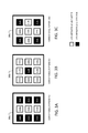
| TABLE 1 |
| Data Structure Identifying a Plurality of LED Groups |
| Group ID | LEDs in Group |
| Group 1 | (1,1), (1,2) (1,3), (2,1) |
| Group 2 | (2,2), (2,3), (3,1) |
| Group 3 | (3,2), (3,3) |
| TABLE 2 |
| A Data Structure Representing an Operational |
| Pattern for a |
| 0 | 0 | 0 |
| 0 | 1 | 0 |
| 0 | 0 | 0 |
Claims (20)
Priority Applications (10)
| Application Number | Priority Date | Filing Date | Title |
|---|---|---|---|
| US15/948,642 US10285236B2 (en) | 2017-09-08 | 2018-04-09 | Optoelectronic device and adaptive illumination system using the same |
| PCT/US2018/049533 WO2019050939A1 (en) | 2017-09-08 | 2018-09-05 | Optoelectronic device and adaptive illumination system using the same |
| TW107131485A TWI782084B (en) | 2017-09-08 | 2018-09-07 | Optoelectronic device and adaptive illumination system using the same |
| JP2018167616A JP6641435B2 (en) | 2017-09-08 | 2018-09-07 | Optoelectronic device and adaptive lighting system using same |
| KR1020180107183A KR102026613B1 (en) | 2017-09-08 | 2018-09-07 | Optoelectronic device and adaptive illumination system using the same |
| CN201811051885.2A CN109469839B (en) | 2017-09-08 | 2018-09-10 | Optoelectronic devices and adaptive lighting systems using the same |
| US16/365,876 US10813184B2 (en) | 2017-09-08 | 2019-03-27 | Optoelectronic device and adaptive illumination system using the same |
| JP2019237624A JP7000410B2 (en) | 2017-09-08 | 2019-12-27 | Optoelectronic devices and adaptive lighting systems that use them |
| US17/021,320 US11435225B2 (en) | 2017-09-08 | 2020-09-15 | Optoelectronic device and adaptive illumination system using the same |
| US17/873,792 US11959800B2 (en) | 2017-09-08 | 2022-07-26 | Optoelectronic device and adaptive illumination system using the same |
Applications Claiming Priority (2)
| Application Number | Priority Date | Filing Date | Title |
|---|---|---|---|
| US15/699,573 US9974135B1 (en) | 2017-09-08 | 2017-09-08 | Optoelectronic device and adaptive illumination system using the same |
| US15/948,642 US10285236B2 (en) | 2017-09-08 | 2018-04-09 | Optoelectronic device and adaptive illumination system using the same |
Related Parent Applications (1)
| Application Number | Title | Priority Date | Filing Date |
|---|---|---|---|
| US15/699,573 Continuation US9974135B1 (en) | 2017-09-08 | 2017-09-08 | Optoelectronic device and adaptive illumination system using the same |
Related Child Applications (1)
| Application Number | Title | Priority Date | Filing Date |
|---|---|---|---|
| US16/365,876 Continuation US10813184B2 (en) | 2017-09-08 | 2019-03-27 | Optoelectronic device and adaptive illumination system using the same |
Publications (2)
| Publication Number | Publication Date |
|---|---|
| US20190082508A1 US20190082508A1 (en) | 2019-03-14 |
| US10285236B2 true US10285236B2 (en) | 2019-05-07 |
Family
ID=62091448
Family Applications (5)
| Application Number | Title | Priority Date | Filing Date |
|---|---|---|---|
| US15/699,573 Active US9974135B1 (en) | 2017-09-08 | 2017-09-08 | Optoelectronic device and adaptive illumination system using the same |
| US15/948,642 Active US10285236B2 (en) | 2017-09-08 | 2018-04-09 | Optoelectronic device and adaptive illumination system using the same |
| US16/365,876 Active US10813184B2 (en) | 2017-09-08 | 2019-03-27 | Optoelectronic device and adaptive illumination system using the same |
| US17/021,320 Active 2037-11-14 US11435225B2 (en) | 2017-09-08 | 2020-09-15 | Optoelectronic device and adaptive illumination system using the same |
| US17/873,792 Active US11959800B2 (en) | 2017-09-08 | 2022-07-26 | Optoelectronic device and adaptive illumination system using the same |
Family Applications Before (1)
| Application Number | Title | Priority Date | Filing Date |
|---|---|---|---|
| US15/699,573 Active US9974135B1 (en) | 2017-09-08 | 2017-09-08 | Optoelectronic device and adaptive illumination system using the same |
Family Applications After (3)
| Application Number | Title | Priority Date | Filing Date |
|---|---|---|---|
| US16/365,876 Active US10813184B2 (en) | 2017-09-08 | 2019-03-27 | Optoelectronic device and adaptive illumination system using the same |
| US17/021,320 Active 2037-11-14 US11435225B2 (en) | 2017-09-08 | 2020-09-15 | Optoelectronic device and adaptive illumination system using the same |
| US17/873,792 Active US11959800B2 (en) | 2017-09-08 | 2022-07-26 | Optoelectronic device and adaptive illumination system using the same |
Country Status (1)
| Country | Link |
|---|---|
| US (5) | US9974135B1 (en) |
Cited By (3)
| Publication number | Priority date | Publication date | Assignee | Title |
|---|---|---|---|---|
| US10813184B2 (en) | 2017-09-08 | 2020-10-20 | Lumileds Llc | Optoelectronic device and adaptive illumination system using the same |
| US11489005B2 (en) | 2019-12-13 | 2022-11-01 | Lumileds Llc | Segmented LED arrays with diffusing elements |
| US11680696B2 (en) | 2019-12-13 | 2023-06-20 | Lumileds Llc | Segmented LED arrays with diffusing elements |
Families Citing this family (12)
| Publication number | Priority date | Publication date | Assignee | Title |
|---|---|---|---|---|
| JP7040144B2 (en) * | 2018-03-08 | 2022-03-23 | コニカミノルタ株式会社 | Optical writing device and image forming device |
| DE102018211929B4 (en) * | 2018-07-18 | 2025-09-25 | Bayerische Motoren Werke Aktiengesellschaft | Method for operating a lighting device in a motor vehicle |
| CN108709638B (en) * | 2018-07-27 | 2021-01-08 | 维沃移动通信有限公司 | A kind of LED circuit, electronic equipment and detection method |
| FR3088408B1 (en) * | 2018-11-09 | 2020-11-13 | Valeo Vision | LIGHT DEVICE FOR A MOTOR VEHICLE INCLUDING A MATRIX LIGHT SOURCE |
| JP7320970B2 (en) * | 2019-03-28 | 2023-08-04 | 株式会社ジャパンディスプレイ | Display device |
| EP3813487B1 (en) * | 2019-10-25 | 2021-12-15 | Lumileds LLC | Automotive led lighting module |
| KR102796591B1 (en) | 2019-12-23 | 2025-04-22 | 서울반도체 주식회사 | Head lamp device |
| FR3116409B1 (en) * | 2020-11-18 | 2022-12-16 | Valeo Vision | LIGHTING SYSTEM FOR MOTOR VEHICLES |
| US11718220B2 (en) * | 2021-01-19 | 2023-08-08 | Infineon Technologies Ag | Compensating for failed pixels in pixelated vehicle headlamps |
| US11671695B2 (en) * | 2021-04-08 | 2023-06-06 | Google Llc | Systems and methods for detecting tampering with privacy notifiers in recording systems |
| US12088909B2 (en) | 2022-06-15 | 2024-09-10 | Google Llc | Warning light thwart detection for recording devices |
| US12422135B2 (en) | 2023-05-03 | 2025-09-23 | Connaught Electronics Ltd. | Vehicle lighting system having illumination characteristics that vary based on detected object class |
Citations (15)
| Publication number | Priority date | Publication date | Assignee | Title |
|---|---|---|---|---|
| JPH0426159A (en) | 1990-05-22 | 1992-01-29 | Ricoh Co Ltd | Semiconductor light-integration device |
| JPH0485962A (en) | 1990-07-30 | 1992-03-18 | Ricoh Co Ltd | Semiconductor light emitter |
| US20060012986A1 (en) | 2004-07-19 | 2006-01-19 | Joseph Mazzochette | LED array package with internal feedback and control |
| JP2008300170A (en) | 2007-05-31 | 2008-12-11 | Hitachi Displays Ltd | LIGHTING DEVICE AND LIQUID CRYSTAL DISPLAY DEVICE USING THE LIGHTING DEVICE |
| JP2009134877A (en) | 2007-11-28 | 2009-06-18 | Sharp Corp | Lighting apparatus |
| JP2009187860A (en) | 2008-02-08 | 2009-08-20 | Denso Corp | Manufacturing method of organic EL element |
| US20100001300A1 (en) | 2008-06-25 | 2010-01-07 | Soraa, Inc. | COPACKING CONFIGURATIONS FOR NONPOLAR GaN AND/OR SEMIPOLAR GaN LEDs |
| US8258707B2 (en) | 2007-04-20 | 2012-09-04 | Koninklijke Philips Electronics N.V. | Lighting device with a LED used for sensing |
| US20140028197A1 (en) | 2012-07-30 | 2014-01-30 | Cree, Inc. | Lighting device with variable color rendering based on ambient light |
| JP2015018612A (en) | 2013-07-08 | 2015-01-29 | パナソニック株式会社 | Lighting device |
| US9041697B2 (en) | 2011-01-28 | 2015-05-26 | Broadcom Corporation | Apparatus and method for using an LED for backlighting and ambient light sensing |
| US20150219300A1 (en) | 2012-08-28 | 2015-08-06 | Mitsubishi Electric Corporation | Light source for head light and head light |
| US20170126944A1 (en) | 2014-06-26 | 2017-05-04 | Koninklijke Philips N.V. | Led lighting unit |
| US20170253172A1 (en) | 2016-03-02 | 2017-09-07 | Valeo Vision | Anti-dazzle headlamp |
| US9847446B2 (en) | 2013-03-28 | 2017-12-19 | Aledia | Electroluminescent device with integrated sensor and method for controlling the emission of the device |
Family Cites Families (17)
| Publication number | Priority date | Publication date | Assignee | Title |
|---|---|---|---|---|
| US8538636B2 (en) * | 1995-06-07 | 2013-09-17 | American Vehicular Sciences, LLC | System and method for controlling vehicle headlights |
| US7066628B2 (en) | 2001-03-29 | 2006-06-27 | Fiber Optic Designs, Inc. | Jacketed LED assemblies and light strings containing same |
| JP4085962B2 (en) | 2003-03-31 | 2008-05-14 | 松下電工株式会社 | Manufacturing method of fiber board |
| JP4247672B2 (en) | 2003-09-10 | 2009-04-02 | ソニー株式会社 | Mobile communication device and mobile communication method |
| EP1784055A3 (en) | 2005-10-17 | 2009-08-05 | Semiconductor Energy Laboratory Co., Ltd. | Lighting system |
| TW200816870A (en) | 2006-09-21 | 2008-04-01 | Beyond Innovation Tech Co Ltd | Circuit and method for driving light source |
| JP4607846B2 (en) | 2006-10-19 | 2011-01-05 | ソニー株式会社 | Light source device, light source driving device, light emission amount control device, and liquid crystal display device |
| JP4026159B1 (en) | 2007-01-19 | 2007-12-26 | 共和コンクリート工業株式会社 | Sea urchin migration prevention method and apparatus |
| JP2009196547A (en) | 2008-02-22 | 2009-09-03 | Toyota Motor Corp | Anti-dazzle device |
| TW201306643A (en) | 2011-07-20 | 2013-02-01 | Winstar Display Co Ltd | AC direct drive organic light emitting diode assembly |
| KR20140124824A (en) * | 2012-02-06 | 2014-10-27 | 애버리 데니슨 코포레이션 | Direction active projection |
| US9308858B2 (en) | 2012-07-13 | 2016-04-12 | Lg Innotek Co., Ltd. | Lamp unit and lighting system for vehicle |
| JP6171439B2 (en) | 2013-03-19 | 2017-08-02 | 三菱自動車工業株式会社 | Visible light communication apparatus and method |
| CN205149636U (en) | 2015-12-11 | 2016-04-13 | 长安大学 | Far and near fiber lamp automatic switching device of meeting at night |
| US11255663B2 (en) * | 2016-03-04 | 2022-02-22 | May Patents Ltd. | Method and apparatus for cooperative usage of multiple distance meters |
| WO2019050939A1 (en) | 2017-09-08 | 2019-03-14 | Lumileds Llc | Optoelectronic device and adaptive illumination system using the same |
| US9974135B1 (en) | 2017-09-08 | 2018-05-15 | Lumileds Llc | Optoelectronic device and adaptive illumination system using the same |
-
2017
- 2017-09-08 US US15/699,573 patent/US9974135B1/en active Active
-
2018
- 2018-04-09 US US15/948,642 patent/US10285236B2/en active Active
-
2019
- 2019-03-27 US US16/365,876 patent/US10813184B2/en active Active
-
2020
- 2020-09-15 US US17/021,320 patent/US11435225B2/en active Active
-
2022
- 2022-07-26 US US17/873,792 patent/US11959800B2/en active Active
Patent Citations (15)
| Publication number | Priority date | Publication date | Assignee | Title |
|---|---|---|---|---|
| JPH0426159A (en) | 1990-05-22 | 1992-01-29 | Ricoh Co Ltd | Semiconductor light-integration device |
| JPH0485962A (en) | 1990-07-30 | 1992-03-18 | Ricoh Co Ltd | Semiconductor light emitter |
| US20060012986A1 (en) | 2004-07-19 | 2006-01-19 | Joseph Mazzochette | LED array package with internal feedback and control |
| US8258707B2 (en) | 2007-04-20 | 2012-09-04 | Koninklijke Philips Electronics N.V. | Lighting device with a LED used for sensing |
| JP2008300170A (en) | 2007-05-31 | 2008-12-11 | Hitachi Displays Ltd | LIGHTING DEVICE AND LIQUID CRYSTAL DISPLAY DEVICE USING THE LIGHTING DEVICE |
| JP2009134877A (en) | 2007-11-28 | 2009-06-18 | Sharp Corp | Lighting apparatus |
| JP2009187860A (en) | 2008-02-08 | 2009-08-20 | Denso Corp | Manufacturing method of organic EL element |
| US20100001300A1 (en) | 2008-06-25 | 2010-01-07 | Soraa, Inc. | COPACKING CONFIGURATIONS FOR NONPOLAR GaN AND/OR SEMIPOLAR GaN LEDs |
| US9041697B2 (en) | 2011-01-28 | 2015-05-26 | Broadcom Corporation | Apparatus and method for using an LED for backlighting and ambient light sensing |
| US20140028197A1 (en) | 2012-07-30 | 2014-01-30 | Cree, Inc. | Lighting device with variable color rendering based on ambient light |
| US20150219300A1 (en) | 2012-08-28 | 2015-08-06 | Mitsubishi Electric Corporation | Light source for head light and head light |
| US9847446B2 (en) | 2013-03-28 | 2017-12-19 | Aledia | Electroluminescent device with integrated sensor and method for controlling the emission of the device |
| JP2015018612A (en) | 2013-07-08 | 2015-01-29 | パナソニック株式会社 | Lighting device |
| US20170126944A1 (en) | 2014-06-26 | 2017-05-04 | Koninklijke Philips N.V. | Led lighting unit |
| US20170253172A1 (en) | 2016-03-02 | 2017-09-07 | Valeo Vision | Anti-dazzle headlamp |
Cited By (5)
| Publication number | Priority date | Publication date | Assignee | Title |
|---|---|---|---|---|
| US10813184B2 (en) | 2017-09-08 | 2020-10-20 | Lumileds Llc | Optoelectronic device and adaptive illumination system using the same |
| US11435225B2 (en) | 2017-09-08 | 2022-09-06 | Lumileds Llc | Optoelectronic device and adaptive illumination system using the same |
| US11959800B2 (en) | 2017-09-08 | 2024-04-16 | Lumileds Llc | Optoelectronic device and adaptive illumination system using the same |
| US11489005B2 (en) | 2019-12-13 | 2022-11-01 | Lumileds Llc | Segmented LED arrays with diffusing elements |
| US11680696B2 (en) | 2019-12-13 | 2023-06-20 | Lumileds Llc | Segmented LED arrays with diffusing elements |
Also Published As
| Publication number | Publication date |
|---|---|
| US20200413500A1 (en) | 2020-12-31 |
| US20220364913A1 (en) | 2022-11-17 |
| US11435225B2 (en) | 2022-09-06 |
| US10813184B2 (en) | 2020-10-20 |
| US20190223267A1 (en) | 2019-07-18 |
| US11959800B2 (en) | 2024-04-16 |
| US20190082508A1 (en) | 2019-03-14 |
| US9974135B1 (en) | 2018-05-15 |
Similar Documents
| Publication | Publication Date | Title |
|---|---|---|
| US11959800B2 (en) | Optoelectronic device and adaptive illumination system using the same | |
| CN109469839B (en) | Optoelectronic devices and adaptive lighting systems using the same | |
| KR101457245B1 (en) | Light emitting module and method for the production of a light emitting module | |
| US6250774B1 (en) | Luminaire | |
| TWI863984B (en) | Led with active region disposed within an optical cavity defined by an embedded nanostructured layer and a reflector | |
| CN108713316B (en) | Optoelectronic lighting device, method for illuminating scene, camera and mobile terminal | |
| TWI742589B (en) | Color tunable light emitting diode (led) systems, led lighting systems, and methods | |
| US20060018512A1 (en) | Vehicle automatic exterior light control | |
| CN107631268B (en) | Lighting and/or signalling device for a motor vehicle | |
| KR20170017847A (en) | Lighting and/or signaling device for an automotive vehicle | |
| EP3399226B1 (en) | Light emitting device, optical module comprising same device, and vehicle comprising same module | |
| KR20150129408A (en) | Light emitting module and lighting apparatus having the same | |
| KR20230025492A (en) | Displays, display devices, and methods for operating displays | |
| US20230358373A1 (en) | Illumination device | |
| KR20230008921A (en) | Led array module | |
| CN114270545B (en) | LED DBR structure with reduced photodegradation | |
| JP7016875B2 (en) | Luminous module | |
| KR20160047060A (en) | Lighting apparatus | |
| JP7101785B2 (en) | Fluorescent material with a light barrier | |
| US20130201669A1 (en) | Led illumination apparatus with improved output uniformity | |
| US10766402B2 (en) | Lighting module having light-emitting elements with gradual cutoff | |
| WO2008081376A2 (en) | Lighting device with a plurality of oled units |
Legal Events
| Date | Code | Title | Description |
|---|---|---|---|
| FEPP | Fee payment procedure |
Free format text: ENTITY STATUS SET TO UNDISCOUNTED (ORIGINAL EVENT CODE: BIG.); ENTITY STATUS OF PATENT OWNER: LARGE ENTITY |
|
| AS | Assignment |
Owner name: LUMILEDS LLC, CALIFORNIA Free format text: ASSIGNMENT OF ASSIGNORS INTEREST;ASSIGNORS:NELSON, ERIK CHARLES;WILDESON, ISAAC;DEB, PARIJAT;AND OTHERS;SIGNING DATES FROM 20180110 TO 20180228;REEL/FRAME:046039/0931 |
|
| STPP | Information on status: patent application and granting procedure in general |
Free format text: AWAITING TC RESP, ISSUE FEE PAYMENT VERIFIED |
|
| STPP | Information on status: patent application and granting procedure in general |
Free format text: PUBLICATIONS -- ISSUE FEE PAYMENT VERIFIED |
|
| STCF | Information on status: patent grant |
Free format text: PATENTED CASE |
|
| MAFP | Maintenance fee payment |
Free format text: PAYMENT OF MAINTENANCE FEE, 4TH YEAR, LARGE ENTITY (ORIGINAL EVENT CODE: M1551); ENTITY STATUS OF PATENT OWNER: LARGE ENTITY Year of fee payment: 4 |
|
| AS | Assignment |
Owner name: DEUTSCHE BANK AG NEW YORK BRANCH, NEW YORK Free format text: PATENT SECURITY AGREEMENT;ASSIGNOR:LUMILEDS, LLC;REEL/FRAME:062114/0001 Effective date: 20221208 |
|
| AS | Assignment |
Owner name: SOUND POINT AGENCY LLC, NEW YORK Free format text: SECURITY INTEREST;ASSIGNORS:LUMILEDS LLC;LUMILEDS HOLDING B.V.;REEL/FRAME:062299/0338 Effective date: 20221230 |
|
| AS | Assignment |
Owner name: LUMILEDS HOLDING B.V., NETHERLANDS Free format text: RELEASE BY SECURED PARTY;ASSIGNOR:SOUND POINT AGENCY LLC;REEL/FRAME:070046/0001 Effective date: 20240731 Owner name: LUMILEDS LLC, CALIFORNIA Free format text: RELEASE BY SECURED PARTY;ASSIGNOR:SOUND POINT AGENCY LLC;REEL/FRAME:070046/0001 Effective date: 20240731 Owner name: LUMILEDS LLC, CALIFORNIA Free format text: RELEASE OF SECURITY INTEREST;ASSIGNOR:SOUND POINT AGENCY LLC;REEL/FRAME:070046/0001 Effective date: 20240731 Owner name: LUMILEDS HOLDING B.V., NETHERLANDS Free format text: RELEASE OF SECURITY INTEREST;ASSIGNOR:SOUND POINT AGENCY LLC;REEL/FRAME:070046/0001 Effective date: 20240731 |
|
| AS | Assignment |
Owner name: LUMILEDS SINGAPORE PTE. LTD., SINGAPORE Free format text: ASSIGNMENT OF ASSIGNORS INTEREST;ASSIGNOR:LUMILEDS LLC;REEL/FRAME:071888/0086 Effective date: 20250708 |