US10277005B2 - Pumped edge emitters with metallic coatings - Google Patents
Pumped edge emitters with metallic coatings Download PDFInfo
- Publication number
- US10277005B2 US10277005B2 US15/703,534 US201715703534A US10277005B2 US 10277005 B2 US10277005 B2 US 10277005B2 US 201715703534 A US201715703534 A US 201715703534A US 10277005 B2 US10277005 B2 US 10277005B2
- Authority
- US
- United States
- Prior art keywords
- metallic
- layer
- facet
- radiation
- reflective coating
- Prior art date
- Legal status (The legal status is an assumption and is not a legal conclusion. Google has not performed a legal analysis and makes no representation as to the accuracy of the status listed.)
- Active
Links
Images


Classifications
-
- H—ELECTRICITY
- H01—ELECTRIC ELEMENTS
- H01S—DEVICES USING THE PROCESS OF LIGHT AMPLIFICATION BY STIMULATED EMISSION OF RADIATION [LASER] TO AMPLIFY OR GENERATE LIGHT; DEVICES USING STIMULATED EMISSION OF ELECTROMAGNETIC RADIATION IN WAVE RANGES OTHER THAN OPTICAL
- H01S5/00—Semiconductor lasers
- H01S5/02—Structural details or components not essential to laser action
- H01S5/028—Coatings ; Treatment of the laser facets, e.g. etching, passivation layers or reflecting layers
- H01S5/0287—Facet reflectivity
-
- H—ELECTRICITY
- H01—ELECTRIC ELEMENTS
- H01S—DEVICES USING THE PROCESS OF LIGHT AMPLIFICATION BY STIMULATED EMISSION OF RADIATION [LASER] TO AMPLIFY OR GENERATE LIGHT; DEVICES USING STIMULATED EMISSION OF ELECTROMAGNETIC RADIATION IN WAVE RANGES OTHER THAN OPTICAL
- H01S3/00—Lasers, i.e. devices using stimulated emission of electromagnetic radiation in the infrared, visible or ultraviolet wave range
- H01S3/09—Processes or apparatus for excitation, e.g. pumping
- H01S3/0955—Processes or apparatus for excitation, e.g. pumping using pumping by high energy particles
- H01S3/0959—Processes or apparatus for excitation, e.g. pumping using pumping by high energy particles by an electron beam
-
- H—ELECTRICITY
- H01—ELECTRIC ELEMENTS
- H01S—DEVICES USING THE PROCESS OF LIGHT AMPLIFICATION BY STIMULATED EMISSION OF RADIATION [LASER] TO AMPLIFY OR GENERATE LIGHT; DEVICES USING STIMULATED EMISSION OF ELECTROMAGNETIC RADIATION IN WAVE RANGES OTHER THAN OPTICAL
- H01S5/00—Semiconductor lasers
- H01S5/04—Processes or apparatus for excitation, e.g. pumping, e.g. by electron beams
-
- H—ELECTRICITY
- H01—ELECTRIC ELEMENTS
- H01S—DEVICES USING THE PROCESS OF LIGHT AMPLIFICATION BY STIMULATED EMISSION OF RADIATION [LASER] TO AMPLIFY OR GENERATE LIGHT; DEVICES USING STIMULATED EMISSION OF ELECTROMAGNETIC RADIATION IN WAVE RANGES OTHER THAN OPTICAL
- H01S5/00—Semiconductor lasers
- H01S5/20—Structure or shape of the semiconductor body to guide the optical wave ; Confining structures perpendicular to the optical axis, e.g. index or gain guiding, stripe geometry, broad area lasers, gain tailoring, transverse or lateral reflectors, special cladding structures, MQW barrier reflection layers
- H01S5/2004—Confining in the direction perpendicular to the layer structure
- H01S5/2018—Optical confinement, e.g. absorbing-, reflecting- or waveguide-layers
-
- H—ELECTRICITY
- H01—ELECTRIC ELEMENTS
- H01S—DEVICES USING THE PROCESS OF LIGHT AMPLIFICATION BY STIMULATED EMISSION OF RADIATION [LASER] TO AMPLIFY OR GENERATE LIGHT; DEVICES USING STIMULATED EMISSION OF ELECTROMAGNETIC RADIATION IN WAVE RANGES OTHER THAN OPTICAL
- H01S5/00—Semiconductor lasers
- H01S5/30—Structure or shape of the active region; Materials used for the active region
- H01S5/32—Structure or shape of the active region; Materials used for the active region comprising PN junctions, e.g. hetero- or double- heterostructures
- H01S5/3211—Structure or shape of the active region; Materials used for the active region comprising PN junctions, e.g. hetero- or double- heterostructures characterised by special cladding layers, e.g. details on band-discontinuities
-
- H—ELECTRICITY
- H01—ELECTRIC ELEMENTS
- H01S—DEVICES USING THE PROCESS OF LIGHT AMPLIFICATION BY STIMULATED EMISSION OF RADIATION [LASER] TO AMPLIFY OR GENERATE LIGHT; DEVICES USING STIMULATED EMISSION OF ELECTROMAGNETIC RADIATION IN WAVE RANGES OTHER THAN OPTICAL
- H01S5/00—Semiconductor lasers
- H01S5/30—Structure or shape of the active region; Materials used for the active region
- H01S5/34—Structure or shape of the active region; Materials used for the active region comprising quantum well or superlattice structures, e.g. single quantum well [SQW] lasers, multiple quantum well [MQW] lasers or graded index separate confinement heterostructure [GRINSCH] lasers
- H01S5/343—Structure or shape of the active region; Materials used for the active region comprising quantum well or superlattice structures, e.g. single quantum well [SQW] lasers, multiple quantum well [MQW] lasers or graded index separate confinement heterostructure [GRINSCH] lasers in AIIIBV compounds, e.g. AlGaAs-laser, InP-based laser
- H01S5/34333—Structure or shape of the active region; Materials used for the active region comprising quantum well or superlattice structures, e.g. single quantum well [SQW] lasers, multiple quantum well [MQW] lasers or graded index separate confinement heterostructure [GRINSCH] lasers in AIIIBV compounds, e.g. AlGaAs-laser, InP-based laser with a well layer based on Ga(In)N or Ga(In)P, e.g. blue laser
-
- H—ELECTRICITY
- H01—ELECTRIC ELEMENTS
- H01S—DEVICES USING THE PROCESS OF LIGHT AMPLIFICATION BY STIMULATED EMISSION OF RADIATION [LASER] TO AMPLIFY OR GENERATE LIGHT; DEVICES USING STIMULATED EMISSION OF ELECTROMAGNETIC RADIATION IN WAVE RANGES OTHER THAN OPTICAL
- H01S5/00—Semiconductor lasers
- H01S5/40—Arrangement of two or more semiconductor lasers, not provided for in groups H01S5/02 - H01S5/30
- H01S5/4025—Array arrangements, e.g. constituted by discrete laser diodes or laser bar
- H01S5/4031—Edge-emitting structures
-
- H—ELECTRICITY
- H01—ELECTRIC ELEMENTS
- H01S—DEVICES USING THE PROCESS OF LIGHT AMPLIFICATION BY STIMULATED EMISSION OF RADIATION [LASER] TO AMPLIFY OR GENERATE LIGHT; DEVICES USING STIMULATED EMISSION OF ELECTROMAGNETIC RADIATION IN WAVE RANGES OTHER THAN OPTICAL
- H01S5/00—Semiconductor lasers
- H01S5/02—Structural details or components not essential to laser action
- H01S5/028—Coatings ; Treatment of the laser facets, e.g. etching, passivation layers or reflecting layers
- H01S5/0286—Coatings with a reflectivity that is not constant over the facets, e.g. apertures
Definitions
- UVR Ultraviolet radiation
- Semiconductor devices can be fabricated to emit radiation at various wavelengths, spanning the visible light spectrum to ultraviolet radiation.
- Ultraviolet radiation (UVR) emitting devices are of considerable interest for applications that include water purification, analytical devices for medical and biotechnology fields, UVR curing, and currency screening, among other applications.
- Radiation emitting devices that emit in spectral ranges suitable for these and other applications can be fabricated based on a variety of semiconductor material systems.
- An edge emitting structure includes an active region configured to generate radiation in response to excitation by a pumping beam incident on the structure.
- a front facet of the edge emitting structure is configured to emit the radiation generated by the active region.
- a metallic reflective coating disposed on at least one of the front and rear facets of the edge emitting structure. The metallic reflective coating is configured to reflect the radiation generated by the active region.
- Some embodiments are directed to a method for making an edge emitting structure.
- the method includes forming an active region configured to generate radiation in response to excitation by a pumping beam incident on the structure.
- One or both of the front and rear facets of the edge emitting structure are coated with a metallic reflective coating.
- the metallic reflective coating is configured to reflect the radiation generated by the active region.
- Some embodiments are directed to a method for operating a edge emitting structure.
- An active region is pumped with a pumping beam.
- the active region In response to the pumping, the active region generates radiation.
- the radiation is reflected from a metallic coating disposed on one or both of front and rear facets of the edge emitting structure. The radiation is emitted through the front facet.
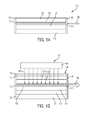
- FIG. 1A is a diagram that illustrates an edge emitting structure in accordance with some embodiments
- FIG. 1B is a diagram of a system that includes an edge emitting structure and an pump source that provides pumping radiation in accordance with some embodiments;
- FIGS. 2A and 2B are diagrams of a system that includes mesa structure in accordance with some embodiments
- FIG. 3 shows the reflectance, transmittance, and absorbance of an aluminum layer on an Al 0.8 Ga 0.2 N surface for a wavelength of 240 nm as a function of layer thickness;
- FIG. 4 shows the light-current (LI) curve for a UVR laser structure in accordance with some embodiments.
- FIG. 5 shows the laser emission spectrum of a laser structure in accordance with some embodiments.
- FIG. 1A is a diagram illustrating an edge emitting structure 101 configured to emit radiation in response to excitation by a pumping beam incident on the edge emitting structure 101 .
- An edge emitter is one in which the generated radiation propagates in a direction along the wafer surface of the semiconductor chip is coupled out at a cleaved edge, referred to herein as a facet.
- the structure 101 shown in FIG. 1A may be a spontaneous edge emitting structure that spontaneously emits radiation in response to the excitation beam pumping.
- the structure 101 may produce stimulated radiation emission in response to the excitation beam pumping.
- the radiation emitted by edge emitting structure 101 may be in the visible light wavelength range, e.g., between about 400 nm to about 700 nm or may be ultraviolet radiation (UVR), e.g., having wavelengths less than 400 nm, less than 300 nm, or even less than 280 nm, for example.
- UVR ultraviolet radiation
- the structure 101 includes an active region 140 optionally disposed on a substrate 110 .
- the substrate 110 may comprise AlN or an AlN template on sapphire or other materials such as Si, SiC, etc.
- AlN templates on sapphire substrates can be prepared by an epitaxial-lateral overgrowth (ELO) technique to achieve a low dislocation-density base layer.
- ELO epitaxial-lateral overgrowth
- the active region 140 may comprise a single layer of material.
- region 140 when the structure 101 is configured as a spontaneous radiation emitter, region 140 may be a single layer of radiation emitting material, such as AlGaN, having a thickness between about 50 nm to about 5 ⁇ m.
- the active region 140 of a spontaneous or stimulated radiation emitter may comprise quantum well structures that include one or more layers of radiation emitting material disposed between barrier layers.
- the active region 140 can include about ten quantum well structures, each quantum well structure comprising at least one quantum well layer disposed between barrier layers.
- the active region 140 comprises Al 0.56 Ga 0.44 N quantum well regions disposed between Al 0.9 Ga 0.1 N barrier layers.
- Such a active region may be grown by metal organic vapor phase epitaxy (MOVPE).
- MOVPE metal organic vapor phase epitaxy
- the thickness of the quantum well layers may be between about 0.5 nm to about 10 nm, e.g., about 1.5 nm, and the thickness of the barrier layers may be between about 2 to about 200 nm, e.g., about 40 nm in this embodiment.
- the total thickness of the active zone may be tailored to the energy deposition profile of the high energy electrons when electron beam pumping is used as excitation method. The optimal thickness is dependent on the energy of the e-beam and might range from about 50 nm to several microns.
- Suitable materials for radiation emission of the active region are group III-V, and II-VI compound semiconductors providing a direct band gap.
- group III-Nitrides e.g., AlGaInN, including B, BAlGaInN
- group III-Arsenides AlGaInAs
- group III-Phosphides AlGaInP
- group III-Sb group III-Sb
- various II-VI compounds such as ZnO, ZnS, ZnSe, and combinations thereof.
- Suitable materials also include diluted semiconductor materials, where part of the group V elements are mixed, e.g., GaNAs, etc.
- the radiation emitting structures disclosed herein may include III-N materials, such as GaN, as well as GaAs, AlGaAs, InGaAs, GaP, InGaP, InP, and GaInP.
- the active region 140 is configured to emit radiation 194 from a front facet 171 of the structure 101 in response to an excitation pump beam incident on the structure.
- Reflective coatings 161 , 162 can be disposed on one or both of the front facet 171 and the rear facet 172 of the structure 101 .
- the structure 101 is edge emitting and the facets 171 are non-parallel with the plane of the active region.
- the reflective coatings 161 , 162 may be metallic, including aluminum or aluminum alloys, or other types of metal.
- each reflective coating 161 , 162 is a single layer of metal, such as a single layer of non-annealed Al.
- the reflective coatings 161 , 162 may extend to cover only portions of the facets 171 , 172 , e.g., the edges of the emitting region 140 or the edges of the emitting region 140 and the edges of the waveguides. In some embodiments, the reflective coatings 161 , 162 may extend to cover substantially all of one or both facets 171 , 172 as shown in FIG. 1A . While aluminum has the highest reflectivity in the ultraviolet radiation range, other metals could be used for devices emitting in other wavelength regions (e.g. silver or gold for the infrared).
- Radiation generated by the active region 140 in response to the pumping is reflected by the reflective metallic coatings 161 , 162 .
- the high reflectivity of the metallic coatings is achieved when being deposited on smooth, mirror-like surfaces. High reflectivities exceeding 90% can be achieved with a single metal film due to the electrically conductive nature of the metal.
- the use of reflective metallic layers is much simpler than relying on constructive interference of multiple reflections at a multi-layered dielectric Distributed Bragg Reflector (DBR), for example.
- DBR Distributed Bragg Reflector
- the edge emitting structure 101 optionally includes a radiation guiding region comprising a lower waveguide 131 disposed over the substrate 110 and an upper waveguide 132 .
- the radiation waveguides 131 , 132 may be omitted if the edge emitting structure 101 is a spontaneous radiation emitter and may be included if the edge emitting structure 101 is a stimulated radiation emitter.
- the active region 140 may be disposed between the lower waveguide 131 and the upper waveguide 132 .
- FIG. 1B is a diagram of a system 100 that includes an edge emitting structure 105 and a pump source 190 that provides pumping beam 193 .
- the pump source 190 may be an optical source that provides an optical pumping beam or may be an electron beam source that provides an electron pumping beam.
- the edge emitting structure 105 comprises a substrate 110 , such as AlN or GaN.
- An optional lower cladding layer 121 is disposed on the substrate 110 .
- An upper cladding layer 122 may be disposed on the opposite side of the active region 140 . The lower may not be needed when the edge emitting structure 105 is a spontaneous emitter.
- the lower cladding layer 122 may comprise Al x Ga 1-x-y In y N, wherein x is between 0.6 and 1 and y is between 0 and 0.3.
- the lower cladding layer 121 comprises n doped Al 0.74 Ga 0.26 N.
- an optional upper cladding layer 122 is present.
- An optional lower waveguide 131 may be formed over the lower cladding layer 121 .
- the lower waveguide 131 comprises Al z Ga 1-z-y In y N where z is between 0.5 and 1, y is between 0 and 0.03, and z ⁇ x.
- the lower waveguide 131 may comprise n-doped Al 0.7 Ga 0.3 N having a thickness of about 40 nm.
- One or both of the lower waveguide 131 and the lower cladding layer 121 may be n-doped.
- the emitting region 140 may be a single layer emitter or a multiple quantum well (MQW) heterostructure formed over the lower waveguide 131 , for example.
- Active emitting region 140 may comprise quantum well-barrier pairs with the quantum well layers comprising Al x Ga 1-x N and the barrier layer comprising Al y Ga 1-y N. In some embodiments, the number of layer pairs is about 5, x is about 0.57 and y is about 0.62.
- the thickness of each quantum well layer may be about 5 nm and the thickness of each barrier layer may be about 9 nm.
- the active region may comprise at least one layer of Al u Ga 1-u-v In v N wherein v is between 0 and 0.03 and 0.4 ⁇ u ⁇ z.
- the barrier layers may be Al s Ga 1-s-t In t N, where 0.4 ⁇ u ⁇ z and s>u+0.04, and t is between 0 and 0.03.
- the quantum well layer thickness may be between 1 and 6 nm and the barrier layer thickness may be between 2 and 20 nm.
- the upper waveguide 132 comprises n-doped AlGaN.
- the upper waveguide 132 may comprise a layer of n-Al 0.7 Ga 0.3 N that is about 40 nm thick, for example.
- upper cladding layer 122 may be formed over upper waveguide 132 .
- the upper waveguide 132 may be relatively thick, e.g., on the order of about 200 nm for example.
- the layer 122 may comprise n-doped AlGaN (such as having at least 70% Al, for example an n-Al 0.78 Ga 0.22 N layer that is 220 nm thick).
- the upper cladding layer 122 may be undoped.
- at least one of the lower cladding layer 121 , lower waveguide layer 131 , emitting region 140 , upper waveguide layer 132 , and upper cladding layer 122 is doped n-type.
- At least one of the lower cladding layer 121 , lower waveguide layer 131 , emitting region 140 , upper waveguide layer 132 , and upper cladding layer 122 is a short-period superlattice.
- at least one of the lower cladding layer 121 , lower waveguide layer 131 , upper waveguide layer 132 , or upper cladding layer 122 may having a monotonically-varying alloy-compositional gradient, with the lower band gap composition of the graded layer nearest the radiation emitting layer.
- At least one of the lower cladding layer 121 , lower waveguide layer 131 , upper waveguide layer 132 , or upper cladding layer 122 may have a monotonically-varying alloy-compositional gradient, with the higher band gap composition of the graded layer nearest the radiation emitting layer.
- the structure 105 shown in FIG. 1B includes metallic reflective coatings 161 , 162 on one or both of the front 171 and rear facets 172 of the structure 105 .
- the reflectivity of the metallic reflective coating can be greater than about 20% and less than about 90% at wavelengths of the emitted radiation.
- a metallic coating may be disposed only on the rear facet or on both the front and rear facets.
- the coating on the rear facet may be an aluminum coating having a thickness of about 1 to about 300 nm, or between about 50 to about 200 nm, e.g., about 100 nm.
- the coating on the front facet is thin enough to allow the radiation generated in the device to exit the device.
- the coating on the front facet may be an aluminum coating having a thickness of about 1 nm to about 100 nm, or between about 5 nm to about 50 nm, or between about 10 to about 30 nm, e.g., about 20 nm.
- Each of the reflective coatings 161 , 162 may be coating applied in one single layer to the facet.
- a reflective coating may be disposed only on the rear facet, in some implementations a reflective coating may only be disposed on the front facet, and in some implementations, reflective coatings may be disposed on both front and rear facets.
- the thickness of the coating on the front facet may be less than the thickness of the coating on the front facet.
- the thickness of the front metallic coating is about 0.1 to about 0.2 times the thickness of the rear metallic coating.
- reflectivity of the metallic reflective coating on the rear facet at wavelengths of the emitted radiation may be between about 80% to about 90%. Reflectivity of the metallic reflective coating on the front facet at the wavelengths of the emitted radiation may be between about 20% to about 70%.
- Metal thicknesses on the front and rear facet can be varied depending on the desired reflectivity.
- the front facet could be uncoated.
- the metal thickness on the front facet is only limited by the light absorption which would totally block the radiation emission beyond a certain thickness.
- a reflective Al layer about 40 nm thick would block radiation at 250 nm emission wavelength.
- III-N material compositions described above are relevant for an example device that emits in the ultraviolet radiation range.
- metal reflective coatings on the front and/or rear facets of pumped, edge emitting devices of any wavelength range are useful, including devices emitting light in the visible range, e.g., green, blue, and red by spontaneous or stimulated emission.
- the semiconductor structures as disclosed herein may be pumped by an optical beam or an electron beam and thus do not rely on a p/n junction for carrier generation.
- the active regions of the edge emitting structures described herein are not embedded between the p and n-type layers of a p/n junction.
- Embodiments disclosed herein involve the use of an optical or electron beam as an excitation source to take advantage of the fact that generation of carriers by optical or beam means that carrier generation and injection does not rely on a p/n-junction. This obviates the challenge of forming a highly conductive (p-type) material in high band gap semiconductors that is able to carry the current densities necessary for radiation emission.
- Electron beam pumping produces a net charge within the device structure.
- light emitting structures disclosed herein include features to allow effective discharge of the structure.
- device structures may include conductive layers that are n-doped (and may include p-doped layers), metal films and/or contacts and connections to ground or the anode of the electron beam source.
- the light emitting device structure 101 , 105 may include a contact layer 151 over the cladding layer 122 , or over the upper waveguide layer 132 if no cladding layer is used, to provide a discharge path for excess charges accumulating due to electron beam pumping.
- the contact layer 151 may comprise n-(Al)GaN as one example.
- a suitable ohmic metal contact layer 152 such as a Ti layer, may be formed over contact layer 151 .
- the ohmic metal layer 152 is thin such that the electron beam can easily penetrate into the emitting region 140 of the structure 101 .
- the contact layer 151 and ohmic metal layer 152 permit conduction of charge from the structure 105 and do not induce extensive absorption losses for the laser mode.
- the edge emitting structure 201 a may not include a top contact layer and/or a top ohmic metal contact layer.
- the upper cladding layer 122 may comprise undoped AlN having a thickness of about 120 nm. Lower absorption losses may be obtained for a thinner upper cladding layer (about 120 nm) as compared to the thicker cladding layer (about 220 nm) described above as used in conjunction with the contact layer and ohmic metal contact layer ( FIGS. 1A and 1B ).
- the lack of a contact layer and ohmic metal contact layer means that the discharge of the device is provided not via these layers on the top side of the light emitting structure, but instead optionally through the n-AlGaN lower cladding layer 121 and/or optionally laterally via the front and rear contacts 271 , 272 disposed respectively on the front and rear sides (facets) 291 , 292 of the light emitting structure 201 a (shown in FIG. 2A ) or side contacts 273 , 274 disposed respectively on the right side and left sidewalls 293 , 294 of the light emitting structure 201 b shown in FIG. 2B ).
- the rear metal contact 272 may partially or fully cover the rear metal reflective coating 162 as shown in FIG. 2A .
- the front metal contact 271 if used, partially covers the front metal reflective coating 161 , with a suitable opening 271 a that allows the radiation generated by the structure 201 a to emerge.
- the discharge contacts 271 , 272 , 273 , 274 may comprise a layered metal structure such as Ti/Al/Ti/Au. According to some embodiment, the discharge contacts 271 , 272 , 273 , 274 are annealed at elevated temperatures to form a good ohmic contact.
- the AlGaN composition of the cladding layer may be limited to provide sufficiently high conductivity (e.g., the Al-composition may be about 78%).
- the upper cladding layer may be chosen to be relatively thick, on the order of 220 nm.
- the upper cladding layer 122 may be non-conductive, e.g., the upper cladding layer may be non-conductive AlN. Furthermore, by reducing the thickness of the AlN upper cladding layer, carrier generation and confinement within the quantum well active region may be enhanced. Thus, the upper cladding layer may be selected, as an example, to be on the order of 120 nm thick.
- the light emitting structure may be etched, e.g., to form a mesa 205 , as shown in FIGS. 2A and 2B , to expose the lower cladding layer 121 for electrical contact.
- Metal contacts 271 - 274 may be deposited on selected portions of the exposed surfaces of the mesa, either at the bottom of the etched region 205 a adjacent the mesa 205 or on one or more of the facets or sidewalls 291 - 294 of the mesa 205 , or both, for the discharge conduction path.
- a contact layer and/or top metal ohmic layer are not needed in this design.
- the pump source 190 is disposed over, and in some embodiments, spaced apart and/or separate from from a top surface of light emitting structure 101 , 105 , 201 .
- the pump source may be an optical beam or electron beam.
- the pump source 190 may be connected to a driving voltage such that it produces a line-pattern (e.g., 20 ⁇ m ⁇ 500 ⁇ m) electron beam 193 in a direction toward and into the top surface of light emitting structure 101 , 105 , 201 .
- Ultraviolet radiation emission wavelengths for such a structure may be obtained, depending upon materials and compositions, for example in the range of about 200 nm to about 385 nm.
- Some embodiments disclosed herein use aluminum coatings on one or both of the front and back facets of an electron beam pumped AlGaInN-based light emitting structure that emits radiation in the UV spectral range in response to the electron beam.
- the metallic coatings can be formed by e-beam deposition wherein the edge emitting structure is positioned at about 45° to the aluminum target to facilitate material deposition on the facet.
- Front and rear facets can be coated in two separate process steps differing in the orientation of the wafer and the deposited metal thickness.
- the facets may be positioned in the evaporator facing the metal source instead of the 45° angle described above.
- evaporation methods e.g. sputtering, thermal evaporation, plasma evaporation, etc.
- e-beam evaporation e.g. sputtering, thermal evaporation, plasma evaporation, etc.
- FIG. 3 shows the reflectance, transmittance, and absorbance of an aluminum layer on an Al 0.8 Ga 0.2 N surface for a wavelength of 240 nm as a function of layer thickness.
- an aluminum layer of about 100 nm is deposited on the rear facet to reach a high reflectivity.
- a thinner layer of about 10 to about 20 nm may be deposited, providing a reflectivity to about 40 to about 70% while still maintaining a transmissivity of about 50% to about 19% for the radiation emitted from the active region.
- FIG. 4 shows the light-current (LI) curve of integrated intensity (Integ. Int.) in arbitrary units vs. beam current in ⁇ A for a UVR laser device with a 200 ⁇ m cavity length, 100 nm thick Al coated rear facet and uncoated front facet.
- the e-beam voltage was 18 kV, 5 ⁇ sec pulses were emitted at a frequency of 1 kHz.
- Laser threshold current is about 174 ⁇ A under pulsed operation at low temperature.
- FIG. 5 shows the laser emission spectrum of the laser structure where the e-beam current was set to 400 ⁇ A.
- the full width half maximum (FWHM) of the laser line is 0.17 nm for this device.
- carrier injection into the active zone is typically problematic.
- the top-most quantum wells of the MQW region see a greater injection than the lower wells, and injection distribution in inhomogeneous. This often limits the number of quantum well layers formed in a semiconductor laser device, which affects device performance.
- a lasing structure may be produced requiring no p-type doping. Very homogeneous generation and deep injection into the active region be can be achieved.
- compositions e.g., AlGaN
- materials e.g., InGaN
- material systems group III-arsenides, group III-phosphides, group II-VI systems, etc.
- a relatively thick top waveguide optimized for electron beam energy deposition may be used without using a top cladding layer.
- the top cladding layer may be realized using low-loss non-epitaxial materials (e.g., Al 2 O 3 ).
Landscapes
- Physics & Mathematics (AREA)
- Electromagnetism (AREA)
- Optics & Photonics (AREA)
- Condensed Matter Physics & Semiconductors (AREA)
- General Physics & Mathematics (AREA)
- Geometry (AREA)
- High Energy & Nuclear Physics (AREA)
- Engineering & Computer Science (AREA)
- Plasma & Fusion (AREA)
- Semiconductor Lasers (AREA)
Abstract
Description
Claims (18)
Priority Applications (1)
| Application Number | Priority Date | Filing Date | Title |
|---|---|---|---|
| US15/703,534 US10277005B2 (en) | 2017-09-13 | 2017-09-13 | Pumped edge emitters with metallic coatings |
Applications Claiming Priority (1)
| Application Number | Priority Date | Filing Date | Title |
|---|---|---|---|
| US15/703,534 US10277005B2 (en) | 2017-09-13 | 2017-09-13 | Pumped edge emitters with metallic coatings |
Publications (2)
| Publication Number | Publication Date |
|---|---|
| US20190081457A1 US20190081457A1 (en) | 2019-03-14 |
| US10277005B2 true US10277005B2 (en) | 2019-04-30 |
Family
ID=65632309
Family Applications (1)
| Application Number | Title | Priority Date | Filing Date |
|---|---|---|---|
| US15/703,534 Active US10277005B2 (en) | 2017-09-13 | 2017-09-13 | Pumped edge emitters with metallic coatings |
Country Status (1)
| Country | Link |
|---|---|
| US (1) | US10277005B2 (en) |
Families Citing this family (2)
| Publication number | Priority date | Publication date | Assignee | Title |
|---|---|---|---|---|
| JP2021077669A (en) * | 2019-11-05 | 2021-05-20 | 住友電気工業株式会社 | Quantum cascade laser |
| CN112713500A (en) * | 2020-12-29 | 2021-04-27 | 深圳瑞波光电子有限公司 | Laser radar and laser thereof |
Citations (12)
| Publication number | Priority date | Publication date | Assignee | Title |
|---|---|---|---|---|
| US4731792A (en) * | 1983-06-29 | 1988-03-15 | Matsushita Electric Industrial Co., Ltd. | Semiconductor laser device with decreased light intensity noise |
| US4751710A (en) * | 1984-07-26 | 1988-06-14 | Nec Corporation | Semiconductor laser device |
| US20010043636A1 (en) * | 2000-04-07 | 2001-11-22 | Bewley William W. | Optical pumping injection cavity for optically pumped devices |
| US20030026312A1 (en) | 2001-07-31 | 2003-02-06 | Clayton Richard D. | Monolithically integrated optically-pumped edge-emitting semiconductor laser |
| US6611543B2 (en) | 2000-12-23 | 2003-08-26 | Applied Optoelectronics, Inc. | Vertical-cavity surface-emitting laser with metal mirror and method of fabrication of same |
| US20080089377A1 (en) * | 2006-09-01 | 2008-04-17 | Chie Fukuda | Method for forming a coating film on a facet of a semiconductor laser diode |
| US7800753B1 (en) * | 2004-10-05 | 2010-09-21 | Photon Systems | Spectroscopic chemical analysis methods and apparatus |
| US7856043B2 (en) | 2005-11-09 | 2010-12-21 | Samsung Electronics Co., Ltd. | Vertical external cavity surface emitting laser with pump beam reflector |
| US20130032825A1 (en) | 2010-08-31 | 2013-02-07 | John Gilmary Wasserbauer | Resonant Optical Cavity Semiconductor Light Emitting Device |
| US20140369367A1 (en) | 2013-06-18 | 2014-12-18 | Palo Alto Research Center Incorporated | Structure For Electron-Beam Pumped Edge-Emitting Device and Methods for Producing Same |
| US9118162B2 (en) | 2011-01-14 | 2015-08-25 | University Of Central Florida Research Foundation, Inc. | Composite semiconductor light source pumped by a spontaneous light emitter |
| US20160315449A1 (en) * | 2015-04-27 | 2016-10-27 | Sensor Electronic Technology, Inc. | Electron Beam Pumping for Light Emission |
-
2017
- 2017-09-13 US US15/703,534 patent/US10277005B2/en active Active
Patent Citations (13)
| Publication number | Priority date | Publication date | Assignee | Title |
|---|---|---|---|---|
| US4731792A (en) * | 1983-06-29 | 1988-03-15 | Matsushita Electric Industrial Co., Ltd. | Semiconductor laser device with decreased light intensity noise |
| US4751710A (en) * | 1984-07-26 | 1988-06-14 | Nec Corporation | Semiconductor laser device |
| US20010043636A1 (en) * | 2000-04-07 | 2001-11-22 | Bewley William W. | Optical pumping injection cavity for optically pumped devices |
| US6611543B2 (en) | 2000-12-23 | 2003-08-26 | Applied Optoelectronics, Inc. | Vertical-cavity surface-emitting laser with metal mirror and method of fabrication of same |
| US20030026312A1 (en) | 2001-07-31 | 2003-02-06 | Clayton Richard D. | Monolithically integrated optically-pumped edge-emitting semiconductor laser |
| US7800753B1 (en) * | 2004-10-05 | 2010-09-21 | Photon Systems | Spectroscopic chemical analysis methods and apparatus |
| US7856043B2 (en) | 2005-11-09 | 2010-12-21 | Samsung Electronics Co., Ltd. | Vertical external cavity surface emitting laser with pump beam reflector |
| US20080089377A1 (en) * | 2006-09-01 | 2008-04-17 | Chie Fukuda | Method for forming a coating film on a facet of a semiconductor laser diode |
| US20130032825A1 (en) | 2010-08-31 | 2013-02-07 | John Gilmary Wasserbauer | Resonant Optical Cavity Semiconductor Light Emitting Device |
| US9118162B2 (en) | 2011-01-14 | 2015-08-25 | University Of Central Florida Research Foundation, Inc. | Composite semiconductor light source pumped by a spontaneous light emitter |
| US20140369367A1 (en) | 2013-06-18 | 2014-12-18 | Palo Alto Research Center Incorporated | Structure For Electron-Beam Pumped Edge-Emitting Device and Methods for Producing Same |
| US8964796B2 (en) | 2013-06-18 | 2015-02-24 | Palo Alto Research Center Incorporated | Structure for electron-beam pumped edge-emitting device and methods for producing same |
| US20160315449A1 (en) * | 2015-04-27 | 2016-10-27 | Sensor Electronic Technology, Inc. | Electron Beam Pumping for Light Emission |
Non-Patent Citations (1)
| Title |
|---|
| Tabata-Vakili et al., "Dominance of radiative recombination from electron-beam-pumped deep-UV AlGaN multi-quantum-well heterostructures", Applied Physics Letters 109, 2016, 181105-181105-5. |
Also Published As
| Publication number | Publication date |
|---|---|
| US20190081457A1 (en) | 2019-03-14 |
Similar Documents
| Publication | Publication Date | Title |
|---|---|---|
| Choquette et al. | Vertical-cavity surface emitting lasers: moving from research to manufacturing | |
| US9153938B2 (en) | Laser diode assembly and semiconductor optical amplifier assembly | |
| US5995529A (en) | Infrared light sources with semimetal electron injection | |
| EP1304778A2 (en) | Laser diode | |
| US10153616B2 (en) | Electron beam pumped vertical cavity surface emitting laser | |
| US7030407B2 (en) | Photon emitter and data transmission device | |
| KR101608542B1 (en) | Optoelectronic component | |
| CN102195232B (en) | Mode-locked semiconductor laser device and driving method thereof | |
| US8964796B2 (en) | Structure for electron-beam pumped edge-emitting device and methods for producing same | |
| US20070223549A1 (en) | High-Power Optoelectronic Device with Improved Beam Quality Incorporating A Lateral Mode Filtering Section | |
| JP7479506B2 (en) | Semiconductor laser, LIDAR system, and laser system having semiconductor laser | |
| US10418785B2 (en) | Electron beam pumped non-c-plane UV emitters | |
| US6500688B2 (en) | Interband cascade light emitting device and method of making same | |
| US8513683B2 (en) | Optical integrated semiconductor light emitting device | |
| US10277005B2 (en) | Pumped edge emitters with metallic coatings | |
| US20220102935A1 (en) | Semiconductor device and fabrication method | |
| US11221446B2 (en) | Laser device assembly | |
| US12506323B2 (en) | Semiconductor laser with a horizontal laser element and a vertical laser element, lidar system and production method | |
| WO2010022526A2 (en) | Superluminescent diode, or amplifier chip | |
| US20060023764A1 (en) | Semiconductor laser and method of manufacturing the same | |
| Maximov et al. | Superluminescent Diodes Based on Chirped InGaAs/GaAs Quantum Well-Dot Layers. Photonics 2023, 10, 1090 | |
| JPH09102630A (en) | II-VI group semiconductor light emitting device and semiconductor surface emitting laser | |
| Getty et al. | Segmented 1.55/spl mu/m laser with 400% differential quantum efficiency | |
| Lochner et al. | DARPA CMUVT Contract FA2386-10-1-4152 Final Report Phase II | |
| Narui et al. | Low-noise and low-operation current AlGaAs separated-double-heterostructure lasers |
Legal Events
| Date | Code | Title | Description |
|---|---|---|---|
| FEPP | Fee payment procedure |
Free format text: ENTITY STATUS SET TO UNDISCOUNTED (ORIGINAL EVENT CODE: BIG.); ENTITY STATUS OF PATENT OWNER: LARGE ENTITY |
|
| AS | Assignment |
Owner name: PALO ALTO RESEARCH CENTER INCORPORATED, CALIFORNIA Free format text: ASSIGNMENT OF ASSIGNORS INTEREST;ASSIGNORS:JESCHKE, JORG;WUNDERER, THOMAS;TEEPE, MARK;SIGNING DATES FROM 20170825 TO 20170911;REEL/FRAME:043587/0058 |
|
| STPP | Information on status: patent application and granting procedure in general |
Free format text: PUBLICATIONS -- ISSUE FEE PAYMENT VERIFIED |
|
| STCF | Information on status: patent grant |
Free format text: PATENTED CASE |
|
| MAFP | Maintenance fee payment |
Free format text: PAYMENT OF MAINTENANCE FEE, 4TH YEAR, LARGE ENTITY (ORIGINAL EVENT CODE: M1551); ENTITY STATUS OF PATENT OWNER: LARGE ENTITY Year of fee payment: 4 |
|
| AS | Assignment |
Owner name: XEROX CORPORATION, CONNECTICUT Free format text: ASSIGNMENT OF ASSIGNORS INTEREST;ASSIGNOR:PALO ALTO RESEARCH CENTER INCORPORATED;REEL/FRAME:064038/0001 Effective date: 20230416 |
|
| AS | Assignment |
Owner name: CITIBANK, N.A., AS COLLATERAL AGENT, NEW YORK Free format text: SECURITY INTEREST;ASSIGNOR:XEROX CORPORATION;REEL/FRAME:064760/0389 Effective date: 20230621 |
|
| AS | Assignment |
Owner name: XEROX CORPORATION, CONNECTICUT Free format text: CORRECTIVE ASSIGNMENT TO CORRECT THE REMOVAL OF US PATENTS 9356603, 10026651, 10626048 AND INCLUSION OF US PATENT 7167871 PREVIOUSLY RECORDED ON REEL 064038 FRAME 0001. ASSIGNOR(S) HEREBY CONFIRMS THE ASSIGNMENT;ASSIGNOR:PALO ALTO RESEARCH CENTER INCORPORATED;REEL/FRAME:064161/0001 Effective date: 20230416 |
|
| AS | Assignment |
Owner name: JEFFERIES FINANCE LLC, AS COLLATERAL AGENT, NEW YORK Free format text: SECURITY INTEREST;ASSIGNOR:XEROX CORPORATION;REEL/FRAME:065628/0019 Effective date: 20231117 |
|
| AS | Assignment |
Owner name: XEROX CORPORATION, CONNECTICUT Free format text: TERMINATION AND RELEASE OF SECURITY INTEREST IN PATENTS RECORDED AT RF 064760/0389;ASSIGNOR:CITIBANK, N.A., AS COLLATERAL AGENT;REEL/FRAME:068261/0001 Effective date: 20240206 Owner name: CITIBANK, N.A., AS COLLATERAL AGENT, NEW YORK Free format text: SECURITY INTEREST;ASSIGNOR:XEROX CORPORATION;REEL/FRAME:066741/0001 Effective date: 20240206 |
|
| AS | Assignment |
Owner name: U.S. BANK TRUST COMPANY, NATIONAL ASSOCIATION, AS COLLATERAL AGENT, CONNECTICUT Free format text: FIRST LIEN NOTES PATENT SECURITY AGREEMENT;ASSIGNOR:XEROX CORPORATION;REEL/FRAME:070824/0001 Effective date: 20250411 |
|
| AS | Assignment |
Owner name: U.S. BANK TRUST COMPANY, NATIONAL ASSOCIATION, AS COLLATERAL AGENT, CONNECTICUT Free format text: SECOND LIEN NOTES PATENT SECURITY AGREEMENT;ASSIGNOR:XEROX CORPORATION;REEL/FRAME:071785/0550 Effective date: 20250701 |
|
| AS | Assignment |
Owner name: GENESEE VALLEY INNOVATIONS, LLC, CALIFORNIA Free format text: ASSIGNMENT OF ASSIGNORS INTEREST;ASSIGNOR:XEROX CORPORATION;REEL/FRAME:073562/0677 Effective date: 20250922 |