US10270042B2 - Compound for organic optoelectric device and organic optoelectric device and display device - Google Patents

Compound for organic optoelectric device and organic optoelectric device and display device Download PDF

Info

Publication number
US10270042B2
US10270042B2 US15/461,620 US201715461620A US10270042B2 US 10270042 B2 US10270042 B2 US 10270042B2 US 201715461620 A US201715461620 A US 201715461620A US 10270042 B2 US10270042 B2 US 10270042B2
Authority
US
United States
Prior art keywords
group
substituted
unsubstituted
compound
independently
Prior art date
Legal status (The legal status is an assumption and is not a legal conclusion. Google has not performed a legal analysis and makes no representation as to the accuracy of the status listed.)
Active, expires
Application number
US15/461,620
Other versions
US20170346019A1 (en
Inventor
Hanill LEE
Dongkyu RYU
Dong Min Kang
Eun Sun Yu
Byoungkwan LEE
Sung-Hyun Jung
Sujin HAN
Current Assignee (The listed assignees may be inaccurate. Google has not performed a legal analysis and makes no representation or warranty as to the accuracy of the list.)
Samsung Electronics Co Ltd
Samsung SDI Co Ltd
Original Assignee
Samsung SDI Co Ltd
Priority date (The priority date is an assumption and is not a legal conclusion. Google has not performed a legal analysis and makes no representation as to the accuracy of the date listed.)
Filing date
Publication date
Application filed by Samsung SDI Co Ltd filed Critical Samsung SDI Co Ltd
Assigned to SAMSUNG SDI CO., LTD. reassignment SAMSUNG SDI CO., LTD. ASSIGNMENT OF ASSIGNORS INTEREST (SEE DOCUMENT FOR DETAILS). Assignors: HAN, Sujin, JUNG, SUNG-HYUN, KANG, DONG MIN, LEE, Byoungkwan, RYU, DONGKYU, YU, EUN SUN, LEE, Hanill
Publication of US20170346019A1 publication Critical patent/US20170346019A1/en
Application granted granted Critical
Publication of US10270042B2 publication Critical patent/US10270042B2/en
Assigned to SAMSUNG ELECTRONICS CO., LTD., SAMSUNG SDI CO., LTD. reassignment SAMSUNG ELECTRONICS CO., LTD. ASSIGNMENT OF ASSIGNORS INTEREST (SEE DOCUMENT FOR DETAILS). Assignors: SAMSUNG SDI CO., LTD.
Active legal-status Critical Current
Adjusted expiration legal-status Critical

Links

Images

Classifications

    • H01L51/0072
    • CCHEMISTRY; METALLURGY
    • C07ORGANIC CHEMISTRY
    • C07DHETEROCYCLIC COMPOUNDS
    • C07D401/00Heterocyclic compounds containing two or more hetero rings, having nitrogen atoms as the only ring hetero atoms, at least one ring being a six-membered ring with only one nitrogen atom
    • C07D401/14Heterocyclic compounds containing two or more hetero rings, having nitrogen atoms as the only ring hetero atoms, at least one ring being a six-membered ring with only one nitrogen atom containing three or more hetero rings
    • CCHEMISTRY; METALLURGY
    • C07ORGANIC CHEMISTRY
    • C07DHETEROCYCLIC COMPOUNDS
    • C07D403/00Heterocyclic compounds containing two or more hetero rings, having nitrogen atoms as the only ring hetero atoms, not provided for by group C07D401/00
    • C07D403/02Heterocyclic compounds containing two or more hetero rings, having nitrogen atoms as the only ring hetero atoms, not provided for by group C07D401/00 containing two hetero rings
    • C07D403/04Heterocyclic compounds containing two or more hetero rings, having nitrogen atoms as the only ring hetero atoms, not provided for by group C07D401/00 containing two hetero rings directly linked by a ring-member-to-ring-member bond
    • CCHEMISTRY; METALLURGY
    • C07ORGANIC CHEMISTRY
    • C07DHETEROCYCLIC COMPOUNDS
    • C07D487/00Heterocyclic compounds containing nitrogen atoms as the only ring hetero atoms in the condensed system, not provided for by groups C07D451/00 - C07D477/00
    • C07D487/02Heterocyclic compounds containing nitrogen atoms as the only ring hetero atoms in the condensed system, not provided for by groups C07D451/00 - C07D477/00 in which the condensed system contains two hetero rings
    • C07D487/04Ortho-condensed systems
    • CCHEMISTRY; METALLURGY
    • C07ORGANIC CHEMISTRY
    • C07DHETEROCYCLIC COMPOUNDS
    • C07D487/00Heterocyclic compounds containing nitrogen atoms as the only ring hetero atoms in the condensed system, not provided for by groups C07D451/00 - C07D477/00
    • C07D487/12Heterocyclic compounds containing nitrogen atoms as the only ring hetero atoms in the condensed system, not provided for by groups C07D451/00 - C07D477/00 in which the condensed system contains three hetero rings
    • C07D487/14Ortho-condensed systems
    • CCHEMISTRY; METALLURGY
    • C07ORGANIC CHEMISTRY
    • C07DHETEROCYCLIC COMPOUNDS
    • C07D519/00Heterocyclic compounds containing more than one system of two or more relevant hetero rings condensed among themselves or condensed with a common carbocyclic ring system not provided for in groups C07D453/00 or C07D455/00
    • CCHEMISTRY; METALLURGY
    • C09DYES; PAINTS; POLISHES; NATURAL RESINS; ADHESIVES; COMPOSITIONS NOT OTHERWISE PROVIDED FOR; APPLICATIONS OF MATERIALS NOT OTHERWISE PROVIDED FOR
    • C09KMATERIALS FOR MISCELLANEOUS APPLICATIONS, NOT PROVIDED FOR ELSEWHERE
    • C09K11/00Luminescent, e.g. electroluminescent, chemiluminescent materials
    • C09K11/02Use of particular materials as binders, particle coatings or suspension media therefor
    • C09K11/025Use of particular materials as binders, particle coatings or suspension media therefor non-luminescent particle coatings or suspension media
    • CCHEMISTRY; METALLURGY
    • C09DYES; PAINTS; POLISHES; NATURAL RESINS; ADHESIVES; COMPOSITIONS NOT OTHERWISE PROVIDED FOR; APPLICATIONS OF MATERIALS NOT OTHERWISE PROVIDED FOR
    • C09KMATERIALS FOR MISCELLANEOUS APPLICATIONS, NOT PROVIDED FOR ELSEWHERE
    • C09K11/00Luminescent, e.g. electroluminescent, chemiluminescent materials
    • C09K11/06Luminescent, e.g. electroluminescent, chemiluminescent materials containing organic luminescent materials
    • H01L51/0067
    • HELECTRICITY
    • H10SEMICONDUCTOR DEVICES; ELECTRIC SOLID-STATE DEVICES NOT OTHERWISE PROVIDED FOR
    • H10KORGANIC ELECTRIC SOLID-STATE DEVICES
    • H10K50/00Organic light-emitting devices
    • H10K50/10OLEDs or polymer light-emitting diodes [PLED]
    • H10K50/11OLEDs or polymer light-emitting diodes [PLED] characterised by the electroluminescent [EL] layers
    • HELECTRICITY
    • H10SEMICONDUCTOR DEVICES; ELECTRIC SOLID-STATE DEVICES NOT OTHERWISE PROVIDED FOR
    • H10KORGANIC ELECTRIC SOLID-STATE DEVICES
    • H10K85/00Organic materials used in the body or electrodes of devices covered by this subclass
    • H10K85/60Organic compounds having low molecular weight
    • H10K85/649Aromatic compounds comprising a hetero atom
    • H10K85/654Aromatic compounds comprising a hetero atom comprising only nitrogen as heteroatom
    • HELECTRICITY
    • H10SEMICONDUCTOR DEVICES; ELECTRIC SOLID-STATE DEVICES NOT OTHERWISE PROVIDED FOR
    • H10KORGANIC ELECTRIC SOLID-STATE DEVICES
    • H10K85/00Organic materials used in the body or electrodes of devices covered by this subclass
    • H10K85/60Organic compounds having low molecular weight
    • H10K85/649Aromatic compounds comprising a hetero atom
    • H10K85/657Polycyclic condensed heteroaromatic hydrocarbons
    • H10K85/6572Polycyclic condensed heteroaromatic hydrocarbons comprising only nitrogen in the heteroaromatic polycondensed ring system, e.g. phenanthroline or carbazole
    • CCHEMISTRY; METALLURGY
    • C09DYES; PAINTS; POLISHES; NATURAL RESINS; ADHESIVES; COMPOSITIONS NOT OTHERWISE PROVIDED FOR; APPLICATIONS OF MATERIALS NOT OTHERWISE PROVIDED FOR
    • C09KMATERIALS FOR MISCELLANEOUS APPLICATIONS, NOT PROVIDED FOR ELSEWHERE
    • C09K2211/00Chemical nature of organic luminescent or tenebrescent compounds
    • C09K2211/10Non-macromolecular compounds
    • C09K2211/1003Carbocyclic compounds
    • C09K2211/1011Condensed systems
    • CCHEMISTRY; METALLURGY
    • C09DYES; PAINTS; POLISHES; NATURAL RESINS; ADHESIVES; COMPOSITIONS NOT OTHERWISE PROVIDED FOR; APPLICATIONS OF MATERIALS NOT OTHERWISE PROVIDED FOR
    • C09KMATERIALS FOR MISCELLANEOUS APPLICATIONS, NOT PROVIDED FOR ELSEWHERE
    • C09K2211/00Chemical nature of organic luminescent or tenebrescent compounds
    • C09K2211/10Non-macromolecular compounds
    • C09K2211/1018Heterocyclic compounds
    • C09K2211/1025Heterocyclic compounds characterised by ligands
    • C09K2211/1029Heterocyclic compounds characterised by ligands containing one nitrogen atom as the heteroatom
    • CCHEMISTRY; METALLURGY
    • C09DYES; PAINTS; POLISHES; NATURAL RESINS; ADHESIVES; COMPOSITIONS NOT OTHERWISE PROVIDED FOR; APPLICATIONS OF MATERIALS NOT OTHERWISE PROVIDED FOR
    • C09KMATERIALS FOR MISCELLANEOUS APPLICATIONS, NOT PROVIDED FOR ELSEWHERE
    • C09K2211/00Chemical nature of organic luminescent or tenebrescent compounds
    • C09K2211/10Non-macromolecular compounds
    • C09K2211/1018Heterocyclic compounds
    • C09K2211/1025Heterocyclic compounds characterised by ligands
    • C09K2211/1044Heterocyclic compounds characterised by ligands containing two nitrogen atoms as heteroatoms
    • H01L51/5016
    • HELECTRICITY
    • H10SEMICONDUCTOR DEVICES; ELECTRIC SOLID-STATE DEVICES NOT OTHERWISE PROVIDED FOR
    • H10KORGANIC ELECTRIC SOLID-STATE DEVICES
    • H10K2101/00Properties of the organic materials covered by group H10K85/00
    • H10K2101/10Triplet emission

Definitions

  • a compound for an organic optoelectric device, an organic optoelectric device, and a display device are disclosed.
  • organic optoelectric device is a device that converts electrical energy into photoenergy, and vice versa.
  • An organic optoelectric device may be classified as follows in accordance with its driving principles.
  • One is a photoelectric device where excitons are generated by photoenergy, separated into electrons and holes, and are transferred to different electrodes to generate electrical energy
  • the other is a light emitting device where a voltage or a current is supplied to an electrode to generate photoenergy from electrical energy.
  • Examples of the organic optoelectric device may be an organic photoelectric device, an organic light emitting diode, an organic solar cell, and an organic photo conductor drum.
  • an organic light emitting diode (OLED) has recently drawn attention due to an increase in demand for flat panel displays.
  • the organic light emitting diode converts electrical energy into light by applying current to an organic light emitting material and has a structure in which an organic layer is disposed between an anode and a cathode.
  • the organic layer may include a light-emitting layer and optionally an auxiliary layer, and the auxiliary layer may be, for example at least one selected from a hole injection layer, a hole transport layer, an electron blocking layer, an electron transport layer, an electron injection layer, and a hole blocking layer for improving efficiency and stability of an organic light emitting diode.
  • Performance of an organic light emitting diode may be affected by characteristics of the organic layer, and among them, may be mainly affected by characteristics of an organic material of the organic layer.
  • An embodiment provides a compound for an organic optoelectric device capable of realizing an organic optoelectric device having high efficiency and a long life-span.
  • Another embodiment provides an organic optoelectric device including the compound for an organic optoelectric device.
  • Yet another embodiment provides a display device including the organic optoelectric device.
  • a compound for an organic optoelectric device represented by Chemical Formula I is provided.
  • a 1 * to a 4 * are independently C or CR c ,
  • R 1 to R 12 and R c are independently hydrogen, deuterium, a substituted or unsubstituted C1 to C10 alkyl group, a substituted or unsubstituted C6 to C20 aryl group, a substituted or unsubstituted C2 to C30 heteroaryl group, or a combination thereof,
  • R 5 to R 12 are independently present or R 5 and R 6 , R 6 and R 7 , R 7 and R 8 , R 9 and R 10 , R 10 and R 11 , and R 11 and R 12 are optionally fused to form a ring,
  • L 1 and L 2 are independently a single bond, a substituted or unsubstituted C6 to C30 arylene group, or a substituted or unsubstituted C2 to C30 heteroarylene group,
  • R a and R b are independently a substituted or unsubstituted C6 to C30 aryl group, a substituted or unsubstituted C2 to C30 heteroaryl group, or a combination thereof,
  • n1 and n2 are independently an integer of 0 or 1
  • substituted refers to replacement of at least one hydrogen by deuterium, a C1 to C30 alkyl group, a C6 to C30 aryl group, or C2 to C30 heteroaryl group.
  • an organic optoelectric device includes an anode and a cathode facing each other and at least one organic layer disposed between the anode and the cathode, wherein the organic layer includes the compound for an organic optoelectric device.
  • a display device including the organic optoelectric device is provided.
  • An organic optoelectric device having high efficiency and a long life-span may be realized.
  • FIGS. 1 and 2 are cross-sectional views showing organic light emitting diodes according to embodiments.
  • substituted refers to replacement of at least one hydrogen of a substituent or a compound by deuterium, a halogen, a hydroxyl group, an amino group, a substituted or unsubstituted C1 to C30 amine group, a nitro group, a substituted or unsubstituted C1 to C40 silyl group, a C1 to C30 alkyl group, a C1 to C10 alkylsilyl group, a C6 to C30 arylsilyl group, a C3 to C30 cycloalkyl group, a C3 to C30 heterocycloalkyl group, a C6 to C30 aryl group, a C6 to C30 heteroaryl group, a C1 to C20 alkoxy group, a fluoro group, a C1 to C10 trifluoroalkyl group, or a cyano group.
  • hetero refers to one including one to three heteroatoms selected from N, O, S, P, and Si, and remaining carbons in one functional group.
  • alkyl group refers to an aliphatic hydrocarbon group.
  • the alkyl group may be “a saturated alkyl group” without any double bond or triple bond.
  • the alkyl group may be a C1 to C30 alkyl group. More specifically, the alkyl group may be a C1 to C20 alkyl group or a C1 to C10 alkyl group.
  • a C1 to C4 alkyl group may have 1 to 4 carbon atoms in alkyl chain which may be selected from methyl, ethyl, propyl, iso-propyl, n-butyl, iso-butyl, sec-butyl, and t-butyl.
  • alkyl group may be a methyl group, an ethyl group, a propyl group, an isopropyl group, a butyl group, an isobutyl group, a t-butyl group, a pentyl group, a hexyl group, a cyclopropyl group, a cyclobutyl group, a cyclopentyl group, a cyclohexyl group, and the like.
  • aryl group refers to a group including at least one hydrocarbon aromatic moiety
  • two or more hydrocarbon aromatic moieties may be linked by a sigma bond and may be, for example a biphenyl group, a terphenyl group, a quarterphenyl group, and the like, and
  • two or more hydrocarbon aromatic moieties are fused directly or indirectly to provide a non-aromatic fused ring.
  • a non-aromatic fused ring may be a fluorenyl group.
  • the aryl group may include a monocyclic, polycyclic or fused ring polycyclic (i.e., rings sharing adjacent pairs of carbon atoms) functional group.
  • a “heteroaryl group” may refer to an aryl group including one to three heteroatoms selected from N, O, S, P, and Si and remaining carbon. Two or more heteroaryl groups are linked by a sigma bond directly, or when the heteroaryl group includes two or more rings, the two or more rings may be fused. When the heteroaryl group is a fused ring, each ring may include one to three heteroatoms.
  • heteroaryl group may be a pyridinyl group, a pyrimidinyl group, a pyrazinyl group, a pyridazinyl group, a triazinyl group, a quinolinyl group, an isoquinolinyl group, and the like.
  • the substituted or unsubstituted C6 to C30 aryl group and/or the substituted or unsubstituted C2 to C30 heteroaryl group may be a substituted or unsubstituted phenyl group, a substituted or unsubstituted naphthyl group, a substituted or unsubstituted anthracenyl group, a substituted or unsubstituted phenanthryl group, a substituted or unsubstituted naphthacenyl group, a substituted or unsubstituted pyrenyl group, a substituted or unsubstituted biphenyl group, a substituted or unsubstituted p-terphenyl group, a substituted or unsubstituted m-terphenyl group, a substituted or unsubstituted chrysenyl group, a substituted or unsubstituted triphenylenyl group, a
  • hole characteristics refer to an ability to donate an electron to form a hole when an electric field is applied, and that a hole formed in the anode may be easily injected into a light-emitting layer, and a hole formed in a light-emitting layer may be easily transported into an anode and transported in a light-emitting layer due to conductive characteristics according to a highest occupied molecular orbital (HOMO) level.
  • HOMO highest occupied molecular orbital
  • electron characteristics refer to an ability to accept an electron when an electric field is applied, and that an electron formed in a cathode may be easily injected into a light-emitting layer, and an electron formed in a light-emitting layer may be easily transported into a cathode and transported in a light-emitting layer due to conductive characteristics according to a lowest unoccupied molecular orbital (LUMO) level.
  • LUMO lowest unoccupied molecular orbital
  • a compound for an organic optoelectric device according to one embodiment is represented by Chemical Formula I.
  • a 1 * to a 4 * are independently C or CR c ,
  • R 1 to R 12 and R c are independently hydrogen, deuterium, a substituted or unsubstituted C1 to C10 alkyl group, a substituted or unsubstituted C6 to C20 aryl group, a substituted or unsubstituted C2 to C30 heteroaryl group, or a combination thereof.
  • R 5 to R 12 are independently present or R 5 and R 6 , R 6 and R 7 , R 7 and R 8 , R 9 and R 10 , R 10 and R 11 , and R 11 and R 12 are optionally fused to form a ring,
  • L 1 and L 2 are independently a single bond, a substituted or unsubstituted C6 to C30 arylene group, or a substituted or unsubstituted C2 to C30 heteroarylene group,
  • R a and R b are independently a substituted or unsubstituted C6 to C30 aryl group, a substituted or unsubstituted C2 to C30 heteroaryl group, or a combination thereof,
  • n1 and n2 are independently an integer of 0 or 1
  • substituted refers to replacement of at least one hydrogen by deuterium, a C1 to C30 alkyl group, a C6 to C30 aryl group, or a C2 to C30 heteroaryl group.
  • the compound for an organic optoelectric device represented by Chemical Formula I forms an asymmetric steric structure where an azatriphenylene including a “nitrogen (N)” unit is fused with carbazole.
  • linked with b 1 *” or “linked with b 2 *” refers to linking with “N” through “b 1 *” or “b 2 *” and herein b 1 * and b 2 * are single bonds and a 1 * to a 4 * linked with b 1 * or b 2 * may be C.
  • a 1 * to a 4 * that are not linked with b 1 * and b 2 * may be CR c wherein a definition of R c is the same as described above.
  • the “nitrogen(N)” unit of the compound for an organic optoelectric device represented by Chemical Formula I has polarity and interacts with an electrode, and charges may be easily injected and mobility increases, and thereby a driving voltage may be reduced.
  • an intermolecular interaction may be small due to the steric structure of molecules, crystallization of molecules may be suppressed and thereby yield improvement and long life-span of an organic light emitting diode may be expected.
  • the asymmetric structure may make deposition at a low temperature possible, and thus decomposition during deposition may be suppressed and a long life-span may be obtained.
  • the compound for an organic optoelectric device may be, for example represented by one of Chemical Formula I-A, I-B, I-C, I-D, and I-E according to a fused position of the carbazole and additional fusion of the carbazole.
  • R 1 , R 2 , and R 4 to R 12 are independently hydrogen, deuterium, a substituted or unsubstituted C to C10 alkyl group, a substituted or unsubstituted C6 to C20 aryl group, a substituted or unsubstituted C2 to C30 heteroaryl group, or a combination thereof,
  • L 1 and L 2 are independently a single bond, a substituted or unsubstituted C6 to C30 arylene group, or a substituted or unsubstituted C2 to C30 heteroarylene group,
  • R a and R b are independently a substituted or unsubstituted C6 to C30 aryl group, a substituted or unsubstituted C2 to C30 heteroaryl group, or a combination thereof, and
  • the “substituted” refers to replacement of at least one hydrogen by deuterium, a C1 to C30 alkyl group, a C6 to C30 aryl group, or a C2 to C30 heteroaryl group.
  • L 1 and L 2 of Chemical Formula I may independently be a single bond, a substituted or unsubstituted C6 to C30 arylene group, or a substituted or unsubstituted C2 to C30 heteroarylene group, and specifically a single bond, or a substituted or unsubstituted C6 to C30 arylene group.
  • L 1 and L 2 are a substituted or unsubstituted C6 to C30 arylene group, for example, one to four phenyl groups may be linked.
  • L 1 and L 2 may be a single bond, a phenylene group, a biphenylene group, a terphenylene group, a quaterphenylene group, or a combination thereof, and specific examples thereof may be selected from linking groups of Group 1.
  • R a and R b of Chemical Formula I may independently be a substituted or unsubstituted C6 to C30 aryl group, a substituted or unsubstituted C2 to C30 heteroaryl group, or a combination thereof, specifically a substituted or unsubstituted phenyl group, a substituted or unsubstituted biphenyl group, a substituted or unsubstituted terphenyl group, a substituted or unsubstituted quaterphenyl group, a substituted or unsubstituted pyridinyl group, a substituted or unsubstituted pyrimidinyl group, a substituted or unsubstituted triazinyl group, a substituted or unsubstituted quinolinyl group, a substituted or unsubstituted isoquinolinyl group, a substituted or unsubstituted indolyl group, a substituted
  • * is a linking site with an adjacent atom.
  • R 1 to R 12 of Chemical Formula I may independently be hydrogen, deuterium, a substituted or unsubstituted C1 to C10 alkyl group, a substituted or unsubstituted C6 to C20 aryl group, a substituted or unsubstituted C2 to C30 heteroaryl group, or a combination thereof, and specifically hydrogen, deuterium, or a substituted or unsubstituted C6 to C30 aryl group.
  • R 1 to R 12 of Chemical Formula I may independently be hydrogen, deuterium, a substituted or unsubstituted phenyl group, a substituted or unsubstituted naphthyl group, a substituted or unsubstituted biphenyl group, a substituted or unsubstituted terphenyl group, or a substituted or unsubstituted triphenylene group.
  • R 1 , R 2 , and R 5 to R 12 may be all hydrogen, R 3 and R 4 may independently be hydrogen, a phenyl group, a biphenyl group, or a terphenyl group.
  • the compound for an organic optoelectric device may be, for example selected from compounds of Group 3, but is not limited thereto.
  • the organic optoelectric device may be any device to convert electrical energy into photoenergy and vice versa without particular limitation, and may be, for example an organic photoelectric device, an organic light emitting diode, an organic solar cell, and an organic photo-conductor drum.
  • the organic optoelectric device may include an anode and a cathode facing each other, and at least one organic layer between the anode and the cathode, wherein the organic layer includes the compound for an organic optoelectric device.
  • FIGS. 1 and 2 are cross-sectional views showing organic light emitting diodes according to embodiments.
  • an organic light emitting diode 100 includes an anode 120 and a cathode 110 facing each other and an organic layer 105 between the anode 120 and the cathode 110 .
  • the anode 120 may be made of a conductor having a large work function to help hole injection, and may be for example metal, metal oxide and/or a conductive polymer.
  • the anode 120 may be, for example a metal nickel, platinum, vanadium, chromium, copper, zinc, gold, and the like or an alloy thereof; metal oxide such as zinc oxide, indium oxide, indium tin oxide (ITO), indium zinc oxide (IZO), and the like; a combination of metal and oxide such as ZnO and Al or SnO 2 and Sb; a conductive polymer such as poly(3-methylthiophene), poly(3,4-(ethylene-1,2-dioxy)thiophene) (PEDT), polypyrrole, and polyaniline, but is not limited thereto.
  • the cathode 110 may be made of a conductor having a small work function to help electron injection, and may be for example metal, metal oxide and/or a conductive polymer.
  • the cathode 110 may be for example a metal or an alloy thereof such as magnesium, calcium, sodium, potassium, titanium, indium, yttrium, lithium, gadolinium, aluminum silver, tin, lead, cesium, barium, and the like; a multi-layer structure material such as LiF/Al, LiO 2 /Al, LiF/Ca, LiF/Al and BaF 2 /Ca, but is not limited thereto.
  • the organic layer 105 includes a light-emitting layer 130 including the compound for an organic optoelectric device.
  • the light-emitting layer 130 may include, for example the compound for an organic optoelectric device alone, or at least two of the compound for an organic optoelectric device.
  • the compound for an organic optoelectric device may be, for example included as a host of a light-emitting layer and may be, for example included as a green host.
  • an organic light emitting diode 200 further includes a hole auxiliary layer 140 in addition to the light-emitting layer 130 .
  • the hole auxiliary layer 140 may further increase hole injection and/or hole mobility and block electrons between the anode 120 and the light-emitting layer 130 .
  • the hole auxiliary layer 140 may be, for example a hole transport layer, a hole injection layer, and/or an electron blocking layer, and may include at least one layer.
  • the compound for an organic optoelectric device may be included in the light-emitting layer 130 .
  • an organic light emitting diode may further an electron transport layer, an electron injection layer, a hole injection layer, and the like as an organic layer 105 .
  • the organic light emitting diodes 100 and 200 may be manufactured by forming an anode or a cathode on a substrate, forming an organic layer using a dry film formation method such as a vacuum deposition method (evaporation), sputtering, plasma plating, and ion plating, and forming a cathode or an anode thereon.
  • a dry film formation method such as a vacuum deposition method (evaporation), sputtering, plasma plating, and ion plating, and forming a cathode or an anode thereon.
  • the organic light emitting diode may be applied to an organic light emitting display device.
  • 2-chloro-4,6-diphenyl-1,3,5-triazine (100 g, 374 mmol) purchased from Tokyo Chemical Industry Co., Ltd. was dissolved in tetrahydrofuran (THF, 0.8 L) under a nitrogen environment, 3-chlorophenylboronic acid (64.3 g, 411 mmol) purchased from Tokyo Chemical Industry Co., Ltd., tetrakis(triphenylphosphine)palladium (4.32 g, 3.74 mmol), and potassium carbonate saturated in water (129 g, 935 mmol) were added thereto, and the mixture was heated and refluxed at 80° C. for 8 hours.
  • Iodobenzene (9.08 g, 44.5 mmol) purchased from Tokyo Chemical Industry Co., Ltd. was dissolved in toluene (0.15 L) under a nitrogen environment, Intermediate I-15 (20 g, 49.0 mmol), tris(diphenylideneacetone)dipalladium (0) (0.41 g, 0.45 mmol), tris-tert butylphosphine (0.45 g, 2.23 mmol), and sodium tert-butoxide (5.13 g, 53.4 mmol) were sequentially added thereto, and the mixture was heated and refluxed at 110° C. for 12 hours.
  • Intermediate I-8 (10 g, 31.3 mmol) was dissolved in toluene (0.1 L) under a nitrogen environment, intermediate I-11 (13.1 g, 31.3 mmol), tris(diphenylideneacetone)dipalladium(0) (0.28 g, 0.31 mmol), tris-tert butylphosphine (0.32 g, 1.57 mmol), and sodium tert-butoxide (3.61 g, 37.6 mmol) were sequentially added thereto, and the mixture was heated and refluxed at 110° C. for 10 hours.
  • Intermediate I-4 (10 g, 31.3 mmol) was dissolved in toluene (0.1 L) under a nitrogen environment, intermediate I-11 (13.1 g, 31.3 mmol), tris(diphenylideneacetone)dipalladium(0) (0.28 g, 0.31 mmol), tris-tert butylphosphine (0.32 g, 1.57 mmol), and sodium tert-butoxide (3.61 g, 37.6 mmol) were sequentially added thereto, and the mixture was heated and refluxed at 110° C. for 30 hours.
  • Host 1 was synthesized with a reference to Patent KR1196093.
  • Host 2 was synthesized with a reference to KR1486096.
  • Host 3 was synthesized with a reference to KR2011-0042004.
  • An organic light emitting diode was manufactured by using Compound 1 according to Synthesis Example 17 as a host and Ir(PPy) 3 as a dopant.
  • a 1000 ⁇ -thick ITO was used as an anode, and a 1000 ⁇ -thick aluminum (Al) as a cathode.
  • the organic light emitting diode was manufactured in a method of cutting an ITO glass substrate having sheet resistance of 15 ⁇ /cm 2 into a size of 50 mm ⁇ 50 mm ⁇ 0.7 mm, ultrasonic wave-cleaning it in acetone, isopropyl alcohol, and pure water respectively for 15 minutes, and UV ozone-cleaning it for 30 minutes.
  • an 800 ⁇ -thick hole transport layer was formed by depositing N4,N4′-di(naphthalen-1-yl)-N4,N4′-diphenylbiphenyl-4,4′-diamine (NPB) (80 nm) under a vacuum degree of 650 ⁇ 10 ⁇ 7 Pa at a deposition rate of 0.1 to 0.3 nm/s.
  • a 300 ⁇ -thick light-emitting layer was formed by using Compound 1 according to Synthesis Example 16 under the same vacuum deposition condition as above, and herein, Ir(PPy) 3 as a phosphorescent dopant was simultaneously deposited.
  • the phosphorescent dopant was deposited in an amount of 7 wt % based on 100 wt % of the total amount of the light-emitting layer by adjusting a deposition rate.
  • a 50 ⁇ -thick hole blocking layer was formed by depositing bis(2-methyl-8-quinolinolate)-4-(phenylphenolato)aluminum (BAlq) under the same vacuum deposition condition as above.
  • BAlq bis(2-methyl-8-quinolinolate)-4-(phenylphenolato)aluminum
  • a 200 ⁇ -thick electron transport layer was formed by depositing Alq3 under the same vacuum deposition condition as above.
  • LiF and Al were sequentially deposited as a cathode, manufacturing the organic photoelectric device.
  • the organic photoelectric device had a structure of ITO/NPB (80 nm)/EML (Compound 1 (93 wt %)+Ir(PPy)3 (7 wt %), 30 nm)/Balq (5 nm)/Alq3 (20 nm)/LiF (1 nm)/Al (100 nm).
  • Organic light emitting diodes were manufactured according to the same method as Example 1 by respectively using Compound 5, Compound 18, Compound 22, Compound 97 and Compound 141 of Synthesis Example 18 to Synthesis Example 22 instead of Compound 1 of Synthesis Example 17.
  • An organic light emitting diode was manufactured according to the same method as Example 1 except for using CBP instead of Compound 1 of Synthesis Example 17.
  • Organic light emitting diodes were manufactured according to the same method as Example 1 by respectively using Host 1, Host 2, and Host 3 of Synthesis Examples 23 to 25 instead of Compound 1 of Synthesis Example 17.
  • NPB, BAlq, CBP, and Ir(PPy)3 used in the organic light emitting diodes respectively have the following structures.
  • a current density change, a luminance change, and luminous efficiency of each organic light emitting diode according to Examples 1 to 6 and Comparative Examples 1 to 4 were measured.
  • the obtained organic light emitting diodes were measured regarding a current value flowing in the unit device, while increasing the voltage from 0 V to 10 V using a current-voltage meter (Keithley 2400), and the measured current value was divided by area to provide the results.
  • Luminance was measured by using a luminance meter (Minolta Cs-1000A), while the voltage of the organic light emitting diodes was increased from 0 V to 10 V.
  • Example 1 to Example 6 exhibit superbly low driving voltage and high efficiency compared with device results of Comparative Examples 1 to 4.

Landscapes

  • Chemical & Material Sciences (AREA)
  • Organic Chemistry (AREA)
  • Engineering & Computer Science (AREA)
  • Materials Engineering (AREA)
  • Physics & Mathematics (AREA)
  • Spectroscopy & Molecular Physics (AREA)
  • Optics & Photonics (AREA)
  • Electroluminescent Light Sources (AREA)

Abstract

A compound for an organic optoelectric device represented by Chemical Formula I, an organic optoelectric device including the same, and a display device are disclosed. Details of Chemical Formula I are defined in the specification.

Description

CROSS-REFERENCE TO RELATED APPLICATION
This application claims priority to and the benefit of Korean Patent Application No. 10-2016-0067440 filed in the Korean Intellectual Property Office on May 31, 2016, the entire contents of which are incorporated herein by reference.
BACKGROUND OF THE INVENTION (a) Field of the Invention
A compound for an organic optoelectric device, an organic optoelectric device, and a display device are disclosed.
(b) Description of the Related Art
An organic optoelectric device (organic optoelectric diode) is a device that converts electrical energy into photoenergy, and vice versa.
An organic optoelectric device may be classified as follows in accordance with its driving principles. One is a photoelectric device where excitons are generated by photoenergy, separated into electrons and holes, and are transferred to different electrodes to generate electrical energy, and the other is a light emitting device where a voltage or a current is supplied to an electrode to generate photoenergy from electrical energy.
Examples of the organic optoelectric device may be an organic photoelectric device, an organic light emitting diode, an organic solar cell, and an organic photo conductor drum.
Of these, an organic light emitting diode (OLED) has recently drawn attention due to an increase in demand for flat panel displays. The organic light emitting diode converts electrical energy into light by applying current to an organic light emitting material and has a structure in which an organic layer is disposed between an anode and a cathode. Herein, the organic layer may include a light-emitting layer and optionally an auxiliary layer, and the auxiliary layer may be, for example at least one selected from a hole injection layer, a hole transport layer, an electron blocking layer, an electron transport layer, an electron injection layer, and a hole blocking layer for improving efficiency and stability of an organic light emitting diode.
Performance of an organic light emitting diode may be affected by characteristics of the organic layer, and among them, may be mainly affected by characteristics of an organic material of the organic layer.
Particularly, development for an organic material being capable of increasing hole and electron mobility and simultaneously increasing electrochemical stability is needed so that the organic light emitting diode may be applied to a large-size flat panel display.
SUMMARY OF THE INVENTION
An embodiment provides a compound for an organic optoelectric device capable of realizing an organic optoelectric device having high efficiency and a long life-span.
Another embodiment provides an organic optoelectric device including the compound for an organic optoelectric device.
Yet another embodiment provides a display device including the organic optoelectric device.
According to an embodiment, a compound for an organic optoelectric device represented by Chemical Formula I is provided.
Figure US10270042-20190423-C00001
In Chemical Formula I,
a1* to a4* are independently C or CRc,
a1* or a2* is linked with b1*,
a3* or a4* is linked with b2*,
R1 to R12 and Rc are independently hydrogen, deuterium, a substituted or unsubstituted C1 to C10 alkyl group, a substituted or unsubstituted C6 to C20 aryl group, a substituted or unsubstituted C2 to C30 heteroaryl group, or a combination thereof,
R5 to R12 are independently present or R5 and R6, R6 and R7, R7 and R8, R9 and R10, R10 and R11, and R11 and R12 are optionally fused to form a ring,
L1 and L2 are independently a single bond, a substituted or unsubstituted C6 to C30 arylene group, or a substituted or unsubstituted C2 to C30 heteroarylene group,
Ra and Rb are independently a substituted or unsubstituted C6 to C30 aryl group, a substituted or unsubstituted C2 to C30 heteroaryl group, or a combination thereof,
n1 and n2 are independently an integer of 0 or 1, and
1≤n1+n2≤2.
The “substituted” refers to replacement of at least one hydrogen by deuterium, a C1 to C30 alkyl group, a C6 to C30 aryl group, or C2 to C30 heteroaryl group.
According to another embodiment, an organic optoelectric device includes an anode and a cathode facing each other and at least one organic layer disposed between the anode and the cathode, wherein the organic layer includes the compound for an organic optoelectric device.
According to another embodiment, a display device including the organic optoelectric device is provided.
An organic optoelectric device having high efficiency and a long life-span may be realized.
BRIEF DESCRIPTION OF THE DRAWINGS
FIGS. 1 and 2 are cross-sectional views showing organic light emitting diodes according to embodiments.
DETAILED DESCRIPTION
Hereinafter, embodiments of the present disclosure are described in detail. However, these embodiments are exemplary, the present invention is not limited thereto and the present invention is defined by the scope of claims.
As used herein, when a definition is not otherwise provided, “substituted” refers to replacement of at least one hydrogen of a substituent or a compound by deuterium, a halogen, a hydroxyl group, an amino group, a substituted or unsubstituted C1 to C30 amine group, a nitro group, a substituted or unsubstituted C1 to C40 silyl group, a C1 to C30 alkyl group, a C1 to C10 alkylsilyl group, a C6 to C30 arylsilyl group, a C3 to C30 cycloalkyl group, a C3 to C30 heterocycloalkyl group, a C6 to C30 aryl group, a C6 to C30 heteroaryl group, a C1 to C20 alkoxy group, a fluoro group, a C1 to C10 trifluoroalkyl group, or a cyano group.
In the present specification, when specific definition is not otherwise provided, “hetero” refers to one including one to three heteroatoms selected from N, O, S, P, and Si, and remaining carbons in one functional group.
In the present specification, when a definition is not otherwise provided, “alkyl group” refers to an aliphatic hydrocarbon group. The alkyl group may be “a saturated alkyl group” without any double bond or triple bond.
The alkyl group may be a C1 to C30 alkyl group. More specifically, the alkyl group may be a C1 to C20 alkyl group or a C1 to C10 alkyl group. For example, a C1 to C4 alkyl group may have 1 to 4 carbon atoms in alkyl chain which may be selected from methyl, ethyl, propyl, iso-propyl, n-butyl, iso-butyl, sec-butyl, and t-butyl.
Specific examples of the alkyl group may be a methyl group, an ethyl group, a propyl group, an isopropyl group, a butyl group, an isobutyl group, a t-butyl group, a pentyl group, a hexyl group, a cyclopropyl group, a cyclobutyl group, a cyclopentyl group, a cyclohexyl group, and the like.
In the present specification, “aryl group” refers to a group including at least one hydrocarbon aromatic moiety, and
all the elements of the hydrocarbon aromatic moiety have p-orbitals which form conjugation, for example a phenyl group, a naphthyl group, and the like,
two or more hydrocarbon aromatic moieties may be linked by a sigma bond and may be, for example a biphenyl group, a terphenyl group, a quarterphenyl group, and the like, and
two or more hydrocarbon aromatic moieties are fused directly or indirectly to provide a non-aromatic fused ring. For example, it may be a fluorenyl group.
The aryl group may include a monocyclic, polycyclic or fused ring polycyclic (i.e., rings sharing adjacent pairs of carbon atoms) functional group.
In the present specification, a “heteroaryl group” may refer to an aryl group including one to three heteroatoms selected from N, O, S, P, and Si and remaining carbon. Two or more heteroaryl groups are linked by a sigma bond directly, or when the heteroaryl group includes two or more rings, the two or more rings may be fused. When the heteroaryl group is a fused ring, each ring may include one to three heteroatoms.
Specific examples of the heteroaryl group may be a pyridinyl group, a pyrimidinyl group, a pyrazinyl group, a pyridazinyl group, a triazinyl group, a quinolinyl group, an isoquinolinyl group, and the like.
More specifically, the substituted or unsubstituted C6 to C30 aryl group and/or the substituted or unsubstituted C2 to C30 heteroaryl group may be a substituted or unsubstituted phenyl group, a substituted or unsubstituted naphthyl group, a substituted or unsubstituted anthracenyl group, a substituted or unsubstituted phenanthryl group, a substituted or unsubstituted naphthacenyl group, a substituted or unsubstituted pyrenyl group, a substituted or unsubstituted biphenyl group, a substituted or unsubstituted p-terphenyl group, a substituted or unsubstituted m-terphenyl group, a substituted or unsubstituted chrysenyl group, a substituted or unsubstituted triphenylenyl group, a substituted or unsubstituted perylenyl group, a substituted or unsubstituted fluorenyl group, a substituted or unsubstituted indenyl group, a substituted or unsubstituted furanyl group, a substituted or unsubstituted thiophenyl group, a substituted or unsubstituted pyrrolyl group, a substituted or unsubstituted pyrazolyl group, a substituted or unsubstituted imidazolyl group, a substituted or unsubstituted triazolyl group, a substituted or unsubstituted oxazolyl group, a substituted or unsubstituted thiazolyl group, a substituted or unsubstituted oxadiazolyl group, a substituted or unsubstituted thiadiazolyl group, a substituted or unsubstituted pyridyl group, a substituted or unsubstituted pyrimidinyl group, a substituted or unsubstituted pyrazinyl group, a substituted or unsubstituted triazinyl group, a substituted or unsubstituted benzofuranyl group, a substituted or unsubstituted benzothiophenyl group, a substituted or unsubstituted benzimidazolyl group, a substituted or unsubstituted indolyl group, a substituted or unsubstituted quinolinyl group, a substituted or unsubstituted isoquinolinyl group, a substituted or unsubstituted quinazolinyl group, a substituted or unsubstituted quinoxalinyl group, a substituted or unsubstituted naphthyridinyl group, a substituted or unsubstituted benzoxazinyl group, a substituted or unsubstituted benzthiazinyl group, a substituted or unsubstituted acridinyl group, a substituted or unsubstituted phenazinyl group, a substituted or unsubstituted phenothiazinyl group, a substituted or unsubstituted phenoxazinyl group, a substituted or unsubstituted dibenzofuranyl group, or a substituted or unsubstituted dibenzothiophenyl group, or a combination thereof, but are not limited thereto.
In the present specification, hole characteristics refer to an ability to donate an electron to form a hole when an electric field is applied, and that a hole formed in the anode may be easily injected into a light-emitting layer, and a hole formed in a light-emitting layer may be easily transported into an anode and transported in a light-emitting layer due to conductive characteristics according to a highest occupied molecular orbital (HOMO) level.
In addition, electron characteristics refer to an ability to accept an electron when an electric field is applied, and that an electron formed in a cathode may be easily injected into a light-emitting layer, and an electron formed in a light-emitting layer may be easily transported into a cathode and transported in a light-emitting layer due to conductive characteristics according to a lowest unoccupied molecular orbital (LUMO) level.
Hereinafter, a compound for an organic optoelectric device according to an embodiment is described.
A compound for an organic optoelectric device according to one embodiment is represented by Chemical Formula I.
Figure US10270042-20190423-C00002
In Chemical Formula I,
a1* to a4* are independently C or CRc,
a1* or a2* is linked with b1*,
a3* or a4* is linked with b2*,
R1 to R12 and Rc are independently hydrogen, deuterium, a substituted or unsubstituted C1 to C10 alkyl group, a substituted or unsubstituted C6 to C20 aryl group, a substituted or unsubstituted C2 to C30 heteroaryl group, or a combination thereof.
R5 to R12 are independently present or R5 and R6, R6 and R7, R7 and R8, R9 and R10, R10 and R11, and R11 and R12 are optionally fused to form a ring,
L1 and L2 are independently a single bond, a substituted or unsubstituted C6 to C30 arylene group, or a substituted or unsubstituted C2 to C30 heteroarylene group,
Ra and Rb are independently a substituted or unsubstituted C6 to C30 aryl group, a substituted or unsubstituted C2 to C30 heteroaryl group, or a combination thereof,
n1 and n2 are independently an integer of 0 or 1, and
1≤n+n2≤2.
The “substituted” refers to replacement of at least one hydrogen by deuterium, a C1 to C30 alkyl group, a C6 to C30 aryl group, or a C2 to C30 heteroaryl group.
The compound for an organic optoelectric device represented by Chemical Formula I forms an asymmetric steric structure where an azatriphenylene including a “nitrogen (N)” unit is fused with carbazole.
In the present specification, “linked with b1*” or “linked with b2*” refers to linking with “N” through “b1*” or “b2*” and herein b1* and b2* are single bonds and a1* to a4* linked with b1* or b2* may be C.
On the other hand, a1* to a4* that are not linked with b1* and b2* may be CRc wherein a definition of Rc is the same as described above.
The “nitrogen(N)” unit of the compound for an organic optoelectric device represented by Chemical Formula I has polarity and interacts with an electrode, and charges may be easily injected and mobility increases, and thereby a driving voltage may be reduced.
In addition, an intermolecular interaction may be small due to the steric structure of molecules, crystallization of molecules may be suppressed and thereby yield improvement and long life-span of an organic light emitting diode may be expected.
The asymmetric structure may make deposition at a low temperature possible, and thus decomposition during deposition may be suppressed and a long life-span may be obtained.
The compound for an organic optoelectric device may be, for example represented by one of Chemical Formula I-A, I-B, I-C, I-D, and I-E according to a fused position of the carbazole and additional fusion of the carbazole.
Figure US10270042-20190423-C00003
Figure US10270042-20190423-C00004
In Chemical Formulae I-A to I-E,
R1, R2, and R4 to R12 are independently hydrogen, deuterium, a substituted or unsubstituted C to C10 alkyl group, a substituted or unsubstituted C6 to C20 aryl group, a substituted or unsubstituted C2 to C30 heteroaryl group, or a combination thereof,
L1 and L2 are independently a single bond, a substituted or unsubstituted C6 to C30 arylene group, or a substituted or unsubstituted C2 to C30 heteroarylene group,
Ra and Rb are independently a substituted or unsubstituted C6 to C30 aryl group, a substituted or unsubstituted C2 to C30 heteroaryl group, or a combination thereof, and
the “substituted” refers to replacement of at least one hydrogen by deuterium, a C1 to C30 alkyl group, a C6 to C30 aryl group, or a C2 to C30 heteroaryl group.
According to an embodiment, L1 and L2 of Chemical Formula I may independently be a single bond, a substituted or unsubstituted C6 to C30 arylene group, or a substituted or unsubstituted C2 to C30 heteroarylene group, and specifically a single bond, or a substituted or unsubstituted C6 to C30 arylene group.
When L1 and L2 are a substituted or unsubstituted C6 to C30 arylene group, for example, one to four phenyl groups may be linked.
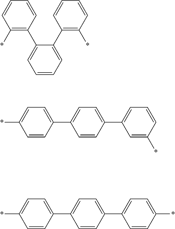
That is, L1 and L2 may be a single bond, a phenylene group, a biphenylene group, a terphenylene group, a quaterphenylene group, or a combination thereof, and specific examples thereof may be selected from linking groups of Group 1.
Figure US10270042-20190423-C00005
Figure US10270042-20190423-C00006
Figure US10270042-20190423-C00007
In Group 1, * is a linking site with an adjacent atom.
According to an embodiment, Ra and Rb of Chemical Formula I may independently be a substituted or unsubstituted C6 to C30 aryl group, a substituted or unsubstituted C2 to C30 heteroaryl group, or a combination thereof, specifically a substituted or unsubstituted phenyl group, a substituted or unsubstituted biphenyl group, a substituted or unsubstituted terphenyl group, a substituted or unsubstituted quaterphenyl group, a substituted or unsubstituted pyridinyl group, a substituted or unsubstituted pyrimidinyl group, a substituted or unsubstituted triazinyl group, a substituted or unsubstituted quinolinyl group, a substituted or unsubstituted isoquinolinyl group, a substituted or unsubstituted indolyl group, a substituted or unsubstituted azaindolyl group, a substituted or unsubstituted benzoxazolyl group, a substituted or unsubstituted benzthiazolyl group, a substituted or unsubstituted azatriphenylenyl group, a substituted or unsubstituted azaphenanthrenyl group, a substituted or unsubstituted quinazolinyl group, or a combination thereof, and specific examples thereof may be linking groups of Group 2.
Figure US10270042-20190423-C00008
Figure US10270042-20190423-C00009
Figure US10270042-20190423-C00010
Figure US10270042-20190423-C00011
In Group 2, * is a linking site with an adjacent atom.
According to an embodiment, R1 to R12 of Chemical Formula I may independently be hydrogen, deuterium, a substituted or unsubstituted C1 to C10 alkyl group, a substituted or unsubstituted C6 to C20 aryl group, a substituted or unsubstituted C2 to C30 heteroaryl group, or a combination thereof, and specifically hydrogen, deuterium, or a substituted or unsubstituted C6 to C30 aryl group.
According to an embodiment, R1 to R12 of Chemical Formula I may independently be hydrogen, deuterium, a substituted or unsubstituted phenyl group, a substituted or unsubstituted naphthyl group, a substituted or unsubstituted biphenyl group, a substituted or unsubstituted terphenyl group, or a substituted or unsubstituted triphenylene group.
For example, R1, R2, and R5 to R12 may be all hydrogen, R3 and R4 may independently be hydrogen, a phenyl group, a biphenyl group, or a terphenyl group.
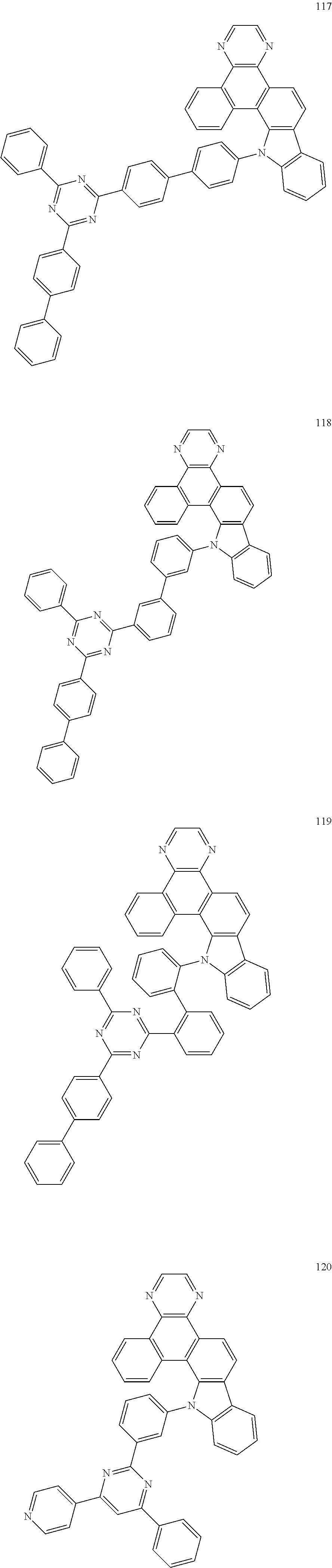
The compound for an organic optoelectric device may be, for example selected from compounds of Group 3, but is not limited thereto.
Figure US10270042-20190423-C00012
Figure US10270042-20190423-C00013
Figure US10270042-20190423-C00014
Figure US10270042-20190423-C00015
Figure US10270042-20190423-C00016
Figure US10270042-20190423-C00017
Figure US10270042-20190423-C00018
Figure US10270042-20190423-C00019
Figure US10270042-20190423-C00020
Figure US10270042-20190423-C00021
Figure US10270042-20190423-C00022
Figure US10270042-20190423-C00023
Figure US10270042-20190423-C00024
Figure US10270042-20190423-C00025
Figure US10270042-20190423-C00026
Figure US10270042-20190423-C00027
Figure US10270042-20190423-C00028
Figure US10270042-20190423-C00029
Figure US10270042-20190423-C00030
Figure US10270042-20190423-C00031
Figure US10270042-20190423-C00032
Figure US10270042-20190423-C00033
Figure US10270042-20190423-C00034
Figure US10270042-20190423-C00035
Figure US10270042-20190423-C00036
Figure US10270042-20190423-C00037
Figure US10270042-20190423-C00038
Figure US10270042-20190423-C00039
Figure US10270042-20190423-C00040
Figure US10270042-20190423-C00041
Figure US10270042-20190423-C00042
Figure US10270042-20190423-C00043
Figure US10270042-20190423-C00044
Figure US10270042-20190423-C00045
Figure US10270042-20190423-C00046
Figure US10270042-20190423-C00047
Hereinafter, an organic optoelectric device including the compound for an organic optoelectric device is described.
The organic optoelectric device may be any device to convert electrical energy into photoenergy and vice versa without particular limitation, and may be, for example an organic photoelectric device, an organic light emitting diode, an organic solar cell, and an organic photo-conductor drum.
The organic optoelectric device may include an anode and a cathode facing each other, and at least one organic layer between the anode and the cathode, wherein the organic layer includes the compound for an organic optoelectric device.
Herein, an organic light emitting diode as one example of an organic optoelectric device is described referring to drawings.
FIGS. 1 and 2 are cross-sectional views showing organic light emitting diodes according to embodiments.
Referring to FIG. 1, an organic light emitting diode 100 according to an embodiment includes an anode 120 and a cathode 110 facing each other and an organic layer 105 between the anode 120 and the cathode 110.
The anode 120 may be made of a conductor having a large work function to help hole injection, and may be for example metal, metal oxide and/or a conductive polymer. The anode 120 may be, for example a metal nickel, platinum, vanadium, chromium, copper, zinc, gold, and the like or an alloy thereof; metal oxide such as zinc oxide, indium oxide, indium tin oxide (ITO), indium zinc oxide (IZO), and the like; a combination of metal and oxide such as ZnO and Al or SnO2 and Sb; a conductive polymer such as poly(3-methylthiophene), poly(3,4-(ethylene-1,2-dioxy)thiophene) (PEDT), polypyrrole, and polyaniline, but is not limited thereto.
The cathode 110 may be made of a conductor having a small work function to help electron injection, and may be for example metal, metal oxide and/or a conductive polymer. The cathode 110 may be for example a metal or an alloy thereof such as magnesium, calcium, sodium, potassium, titanium, indium, yttrium, lithium, gadolinium, aluminum silver, tin, lead, cesium, barium, and the like; a multi-layer structure material such as LiF/Al, LiO2/Al, LiF/Ca, LiF/Al and BaF2/Ca, but is not limited thereto.
The organic layer 105 includes a light-emitting layer 130 including the compound for an organic optoelectric device.
The light-emitting layer 130 may include, for example the compound for an organic optoelectric device alone, or at least two of the compound for an organic optoelectric device.
The compound for an organic optoelectric device according to an embodiment may be, for example included as a host of a light-emitting layer and may be, for example included as a green host.
Referring to FIG. 2, an organic light emitting diode 200 further includes a hole auxiliary layer 140 in addition to the light-emitting layer 130. The hole auxiliary layer 140 may further increase hole injection and/or hole mobility and block electrons between the anode 120 and the light-emitting layer 130. The hole auxiliary layer 140 may be, for example a hole transport layer, a hole injection layer, and/or an electron blocking layer, and may include at least one layer. The compound for an organic optoelectric device may be included in the light-emitting layer 130.
In an embodiment of the present invention, in FIG. 1 or 2, an organic light emitting diode may further an electron transport layer, an electron injection layer, a hole injection layer, and the like as an organic layer 105.
The organic light emitting diodes 100 and 200 may be manufactured by forming an anode or a cathode on a substrate, forming an organic layer using a dry film formation method such as a vacuum deposition method (evaporation), sputtering, plasma plating, and ion plating, and forming a cathode or an anode thereon.
The organic light emitting diode may be applied to an organic light emitting display device.
Hereinafter, the embodiments are illustrated in more detail with reference to examples. These examples, however, are not in any sense to be interpreted as limiting the scope of the invention
(Synthesis of Compound for Organic Optoelectric Device)
Hereinafter, starting materials and reactants used in Examples and Synthesis Examples were purchased from Sigma-Aldrich Co. Ltd. or TCI Inc. as far as there in no particular comment.
Synthesis Example 1: Synthesis of Intermediate I-1
Figure US10270042-20190423-C00048
An intermediate, 3-bromophenanthrene-9,10-dione (50 g, 174 mmol) purchased from Chemirex Co., Ltd. (http://chemirex.com/) was dissolved in 0.5 L of toluene under a nitrogen environment, ethylene diamine (12.6 g, 209 mmol) was added thereto, and the mixture was heated and refluxed for 5 hours. After the reaction was complete, water was added to the reaction solution, the mixture was extracted with dichloromethane (DCM) and treated with anhydrous MgSO4 to remove moisture, and the resultant was filtered and concentrated under a reduced pressure. The obtained residue was separated and purified through flash column chromatography to obtain Intermediate I-1 (40.3 g, 75%).
HRMS (70 eV, EI+): m/z calcd for C16H9BrN2: 307.9949, found: 308.
Elemental Analysis: C, 62%; H, 3%
Synthesis Example 2: Synthesis of Intermediate I-2
Figure US10270042-20190423-C00049
Intermediate I-1 (35 g, 113 mmol) was dissolved in dimethylforamide (DMF, 0.35 L) under a nitrogen environment, bis(pinacolato)diboron (34.5 g, 136 mmol), (1,1′-bis(diphenylphosphine)ferrocene)dichloropalladium (II) (0.92 g, 1.13 mmol), and potassium acetate (33.3 g, 339 mmol) were added thereto, and the mixture was heated and refluxed at 150° C. for 12 hours. When the reaction was complete, water was added to the reaction solution, and the mixture was filtered, and dried in a vacuum oven. The obtained residue was separated and purified through flash column chromatography to obtain Intermediate I-2 (27.8 g, 69%).
HRMS (70 eV, EI+): m/z calcd for C22H21BN2O2: 356.1696, found: 356.
Elemental Analysis: C, 74%; H, 6%
Synthesis Example 3: Synthesis of Intermediate I-3
Figure US10270042-20190423-C00050
Intermediate I-2 (25 g, 70.2 mmol) was dissolved in tetrahydrofuran (THF, 0.2 L) under a nitrogen environment, 1-bromo-2-nitrobenzene (14.2 g, 70.2 mmol) purchased from Tokyo Chemical Industry Co., Ltd., tetrakis(triphenylphosphine)palladium (0.81 g, 0.70 mmol), and potassium carbonate saturated in water (24.3 g, 176 mmol) were added thereto, and the mixture is heated and refluxed at 80° C. for 13 hours. After the reaction was complete, water was added to the reaction solution, the mixture was extracted with dichloromethane (DCM) and treated with anhydrous MgSO4 to remove moisture, and the resultant was filtered and concentrated under a reduced pressure. The obtained residue was separated and purified through flash column chromatography to obtain Intermediate I-3 (20.0 g, 81%).
HRMS (70 eV, EI+): m/z calcd for C22H13N3O2: 351.1008, found: 351.
Elemental Analysis: C, 75%; H, 4%
Synthesis Example 4: Synthesis of Intermediate I-4
Figure US10270042-20190423-C00051
Intermediate I-3 (15 g, 42.7 mmol) was dissolved in triethylphosphite (0.1 L) purchased from Sigma Aldrich Co., Ltd. under a nitrogen environment and then, heated and refluxed at 180° C. for 3 hours. After the reaction was complete, water was added to the reaction solution, the mixture was extracted with dichloromethane (DCM) and treated with anhydrous MgSO4 to remove moisture, and the resultant was filtered and concentrated under a reduced pressure. The obtained residue was separated and purified through flash column chromatography to obtain Intermediate I-4 (8.45 g, 62%).
HRMS (70 eV. EI+): m/z calcd for C22H13N3: 319.1109, found: 319.
Elemental Analysis: C, 83%; H, 4%
Synthesis Example 5: Synthesis of Intermediate I-5
Figure US10270042-20190423-C00052
An intermediate, 3-bromophenanthrene-9,10-dione (100 g, 299 mmol) purchased from Chemirex Co., Ltd. was dissolved in dimethylforamide (DMF, 1.0 L) under a nitrogen environment, bis(pinacolato)diboron (91.2 g, 359 mmol), (1,1′-bis(diphenylphosphine)ferrocene)dichloropalladium (II) (2.44 g, 2.99 mmol), and potassium acetate (88.0 g, 897 mmol) were added thereto, and the mixture was heated and refluxed at 150° C. for 11 hours. When the reaction was complete, water was added to the reaction solution, and the mixture was filtered, and dried in a vacuum oven. The obtained residue was separated and purified through flash column chromatography to obtain Intermediate I-5 (82.9 g, 83%).
HRMS (70 eV, EI+): m/z calcd for C20H19BO4: 334.1376, found: 334.
Elemental Analysis: C, 72%; H, 6%
Synthesis Example 6: Synthesis of Intermediate I-6
Figure US10270042-20190423-C00053
Intermediate I-5 (80 g, 239 mmol) was dissolved in tetrahydrofuran (THF, 0.4 L) under a nitrogen environment, 1-bromo-2-nitrobenzene (48.4 g, 239 mmol) purchased from Tokyo Chemical Industry Co., Ltd., tetrakis(triphenylphosphine)palladium (2.76 g, 2.39 mmol), and potassium carbonate saturated in water (82.6 g, 598 mmol) were added thereto, and the mixture was heated and refluxed at 80° C. for 19 hours. After the reaction was complete, water was added to the reaction solution, the mixture was extracted with dichloromethane (DCM) and treated with anhydrous MgSO4 to remove moisture, and the resultant was filtered and concentrated under a reduced pressure. The obtained residue was separated and purified through flash column chromatography to obtain Intermediate I-6 (23.6 g, 30%).
HRMS (70 eV, EI+): m/z calcd for C20H11NO4: 329.0688, found: 329.
Elemental Analysis: C, 73%; H, 3%
Synthesis Example 7: Synthesis of Intermediate I-7
Figure US10270042-20190423-C00054
Intermediate I-6 (21 g, 63.8 mmol) was dissolved in triethylphosphite (0.1 L) purchased from Sigma Aldrich Co., Ltd. under a nitrogen environment and then, heated and refluxed at 180° C. for 3 hours. After the reaction was complete, water was added to the reaction solution, the mixture was extracted with dichloromethane (DCM) and treated with anhydrous MgSO4 to remove moisture, and the resultant was filtered and concentrated under a reduced pressure. The obtained residue was separated and purified through flash column chromatography to obtain Intermediate I-7 (9.10 g, 48%).
HRMS (70 eV, EI+): m/z calcd for C20H11NO2: 297.0790, found: 297.
Elemental Analysis: C, 81%; H, 4%
Synthesis Example 8: Synthesis of Intermediate I-8
Figure US10270042-20190423-C00055
Intermediate I-7 (8 g, 26.9 mmol) was dissolved in toluene (0.08 L) under a nitrogen environment, ethylene diamine (2.43 g, 40.4 mmol) was added thereto, and the mixture was heated and refluxed for 5 hours. After the reaction was complete, water was added to the reaction solution, the mixture was extracted with dichloromethane (DCM) and treated with anhydrous MgSO4 to remove moisture, and the resultant was filtered and concentrated under a reduced pressure. The obtained residue was separated an purified through flash column chromatography to obtain Intermediate I-8 (6.01 g, 70%).
HRMS (70 eV, EI+): m/z calcd for C22H13N3: 319.1109, found: 319.
Elemental Analysis: C, 83%; H, 4%
Synthesis Example 9: Synthesis of Intermediate I-9
Figure US10270042-20190423-C00056
2-chloro-4,6-diphenyl-1,3,5-triazine (100 g, 374 mmol) purchased from Tokyo Chemical Industry Co., Ltd. was dissolved in tetrahydrofuran (THF, 0.8 L) under a nitrogen environment, 3-chlorophenylboronic acid (64.3 g, 411 mmol) purchased from Tokyo Chemical Industry Co., Ltd., tetrakis(triphenylphosphine)palladium (4.32 g, 3.74 mmol), and potassium carbonate saturated in water (129 g, 935 mmol) were added thereto, and the mixture was heated and refluxed at 80° C. for 8 hours. After the reaction was complete, water was added to the reaction solution, the mixture was extracted with dichloromethane (DCM) and treated with anhydrous MgSO4 to remove moisture, and the resultant was filtered and concentrated under a reduced pressure. The obtained residue was separated and purified through flash column chromatography to obtain Intermediate I-9 (116 g, 90%).
HRMS (70 eV, EI+): m/z calcd for C21H14ClN3: 343.0876, found: 343.
Elemental Analysis: C, 73%; H, 4%
Synthesis Example 10: Synthesis of Intermediate I-10
Figure US10270042-20190423-C00057
Intermediate I-9 (110 g, 320 mmol) was dissolved in dimethylforamide (DMF, 1.0 L) under a nitrogen environment, bis(pinacolato)diboron (97.5 g, 384 mmol), (1,1′-bis(diphenylphosphine)ferrocene)dichloropalladium (II) (2.61 g, 3.20 mmol), and potassium acetate (94.2 g, 960 mmol) were added thereto, and the mixture was heated and refluxed at 150° C. for 24 hours. When the reaction was complete, water was added to the reaction solution, and the mixture was filtered, and dried in a vacuum oven. The obtained residue was separated and purified through flash column chromatography to obtain Intermediate I-10 (97.5 g, 70%).
HRMS (70 eV, EI+): m/z calcd for C27H26BN3O2: 435.2118, found: 435.
Elemental Analysis: C, 74%; H, 6%
Synthesis Example 11: Synthesis of Intermediate I-11
Figure US10270042-20190423-C00058
Intermediate I-10 (95 g, 218 mmol) was dissolved in tetrahydrofuran (THF, 0.7 L) under a nitrogen environment, 1-bromo-3-chlorobenzene (41.8 g, 218 mmol) purchased from Tokyo Chemical Industry Co., Ltd., tetrakis(triphenylphosphine)palladium (2.52 g, 2.18 mmol), and potassium carbonate saturated in water (75.3 g, 545 mmol) were added thereto, and the mixture was heated and refluxed at 80° C. for 10 hours. After the reaction was complete, water was added to the reaction solution, the mixture was extracted with dichloromethane (DCM) and treated with anhydrous MgSO4 to remove moisture, and the resultant was filtered and concentrated under a reduced pressure. The obtained residue was separated and purified through flash column chromatography to obtain Intermediate I-11 (77.8 g, 85%).
HRMS (70 eV, EI+): m/z calcd for C27H18ClN3: 419.1189, found: 419.
Elemental Analysis: C, 77%; H, 4%
Synthesis Example 12: Synthesis of Intermediate I-12
Figure US10270042-20190423-C00059
3,6-dibromophenanthrene-9,10-dione (100 g, 273 mmol) purchased from Chemirex Co., Ltd. was dissolved in dimethylforamide (DMF, 1.4 L) under a nitrogen environment, bis(pinacolato)diboron (173 g, 683 mmol), (1,1′-bis(diphenylphosphine)ferrocene)dichloropalladium (II) (4.46 g, 5.46 mmol), and potassium acetate (134 g, 1,365 mmol) were added thereto, and the mixture was heated and refluxed at 150° C. for 10 hours. When the reaction was complete, water was added to the reaction solution, and the mixture was filtered, and dried in a vacuum oven. The obtained residue was separated and purified through flash column chromatography to obtain Intermediate I-12 (113 g, 90%).
HRMS (70 eV, EI+): m/z calcd for C26H30B2O6: 460.2228, found: 460.
Elemental Analysis: C, 68%; H, 7%
Synthesis Example 13: Synthesis of Intermediate I-13
Figure US10270042-20190423-C00060
Intermediate I-12 (110 g, 239 mmol) was dissolved in tetrahydrofuran (THF, 1.1 L) under a nitrogen environment, 1-bromo-2-nitrobenzene (105 g, 526 mmol) purchased from Tokyo Chemical Industry Co., Ltd., tetrakis(triphenylphosphine)palladium (5.52 g, 4.78 mmol), and potassium carbonate saturated in water (165 g, 1,195 mmol) were added thereto, and the mixture was heated and refluxed at 80° C. for 25 hours. After the reaction was complete, water was added to the reaction solution, the mixture was extracted with dichloromethane (DCM) and treated with anhydrous MgSO4 to remove moisture, and the resultant was filtered and concentrated under a reduced pressure. The obtained residue was separated and purified through flash column chromatography to obtain Intermediate I-13 (38.8 g, 36%).
HRMS (70 eV, EI+): m/z calcd for C26H14N2O6: 450.0852, found: 450.
Elemental Analysis: C, 69%; H, 3%
Synthesis Example 14: Synthesis of Intermediate I-14
Figure US10270042-20190423-C00061
Intermediate I-13 (35 g, 15.8 mmol) was dissolved in triethylphosphite (0.2 L) purchased from Sigma Aldrich Co., Ltd. under a nitrogen environment and then, heated and refluxed at 180° C. for 3 hours. After the reaction was complete, water was added to the reaction solution, the mixture was extracted with dichloromethane (DCM) and treated with anhydrous MgSO4 to remove moisture, and the resultant was filtered and concentrated under a reduced pressure. The obtained residue was separated and purified through flash column chromatography to obtain Intermediate I-14 (9.10 g, 48%).
HRMS (70 eV, EI+): m/z calcd for C26H14N2O2: 386.1055, found: 386.
Elemental Analysis: C, 81%; H, 4%
Synthesis Example 15: Synthesis of Intermediate I-15
Figure US10270042-20190423-C00062
Intermediate I-14 (8 g, 20.7 mmol) was dissolved in toluene (0.08 L) under a nitrogen environment, ethylene diamine (1.87 g, 31.1 mmol) was added thereto, and the mixture was heated and refluxed for 5 hours. After the reaction was complete, water was added to the reaction solution, the mixture was extracted with dichloromethane (DCM) and treated with anhydrous MgSO4 to remove moisture, and the resultant was filtered and concentrated under a reduced pressure. The obtained residue was separated and purified through flash column chromatography to obtain Intermediate I-15 (6.34 g, 75%).
HRMS (70 eV, EI+): m/z calcd for C28H16N4: 408.1375, found: 408.
Elemental Analysis: C, 82%; H, 4%
Synthesis Example 16: Synthesis of Intermediate I-16
Figure US10270042-20190423-C00063
Iodobenzene (9.08 g, 44.5 mmol) purchased from Tokyo Chemical Industry Co., Ltd. was dissolved in toluene (0.15 L) under a nitrogen environment, Intermediate I-15 (20 g, 49.0 mmol), tris(diphenylideneacetone)dipalladium (0) (0.41 g, 0.45 mmol), tris-tert butylphosphine (0.45 g, 2.23 mmol), and sodium tert-butoxide (5.13 g, 53.4 mmol) were sequentially added thereto, and the mixture was heated and refluxed at 110° C. for 12 hours. After the reaction was complete, water was added to the reaction solution, the mixture was extracted with dichloromethane (DCM) and treated with anhydrous MgSO4 to remove moisture, and the resultant was filtered and concentrated under a reduced pressure. The obtained residue was separated and purified through flash column chromatography to obtain Intermediate I-16 (19.4 g, 90%).
HRMS (70 eV, EI+): m/z calcd for C34H20N4: 484.1688, found: 484.
Elemental Analysis: C, 84%; H, 4%
Synthesis Example 17: Synthesis of Compound 1
Figure US10270042-20190423-C00064
Intermediate I-8 (10 g, 31.3 mmol) was dissolved in toluene (0.1 L) under a nitrogen environment, 2-chloro-4,6-diphenyl-1,3,5-triazine (8.38 g, 31.3 mmol) purchased from Tokyo Chemical Industry Co., Ltd., tris(diphenylideneacetone)dipalladium(0) (0.28 g, 0.31 mmol), tris-tert butylphosphine (0.32 g, 1.57 mmol), and sodium tert-butoxide (3.61 g, 37.6 mmol) were sequentially added thereto, and the mixture was heated and refluxed at 110° C. for 13 hours. After the reaction was complete, water was added to the reaction solution, the mixture was extracted with dichloromethane (DCM) and treated with anhydrous MgSO4 to remove moisture, and the resultant was filtered and concentrated under a reduced pressure. The obtained residue was separated and purified through flash column chromatography to obtain Compound 1 (15.2 g, 88%).
HRMS (70 eV, EI+): m/z calcd for C37H22N6: 550.1906, found: 550.
Elemental Analysis: C, 81%; H, 4%
Synthesis Example 18: Synthesis of Compound 5
Figure US10270042-20190423-C00065
Intermediate I-4 (10 g, 31.3 mmol) was dissolved in toluene (0.1 L) under a nitrogen environment, 2-chloro-4,6-diphenyl-1,3,5-triazine (8.38 g, 31.3 mmol) purchased from Tokyo Chemical Industry Co., Ltd., tris(diphenylideneacetone)dipalladium(0) (0.28 g, 0.31 mmol), tris-tert butylphosphine (0.32 g, 1.57 mmol), and sodium tert-butoxide (3.61 g, 37.6 mmol) were sequentially added thereto, and the mixture was heated and refluxed at 110° C. for 25 hours. After the reaction was complete, water was added to the reaction solution, the mixture was extracted with dichloromethane (DCM) and treated with anhydrous MgSO4 to remove moisture, and the resultant was filtered and concentrated under a reduced pressure. The obtained residue was separated and purified through flash column chromatography to obtain Compound 5 (5.51 g, 32%).
HRMS (70 eV, EI+): m/z calcd for C37H22N6: 550.1906, found: 550.
Elemental Analysis: C, 81%; H, 4%
Synthesis Example 19: Synthesis of Compound 18
Figure US10270042-20190423-C00066
Intermediate I-8 (10 g, 31.3 mmol) was dissolved in toluene (0.1 L) under a nitrogen environment, intermediate I-11 (13.1 g, 31.3 mmol), tris(diphenylideneacetone)dipalladium(0) (0.28 g, 0.31 mmol), tris-tert butylphosphine (0.32 g, 1.57 mmol), and sodium tert-butoxide (3.61 g, 37.6 mmol) were sequentially added thereto, and the mixture was heated and refluxed at 110° C. for 10 hours. After the reaction was complete, water was added to the reaction solution, the mixture was extracted with dichloromethane (DCM) and treated with anhydrous MgSO4 to remove moisture, and the resultant was filtered and concentrated under a reduced pressure. The obtained residue was separated and purified through flash column chromatography to obtain Compound 18 (20.5 g, 93%).
HRMS (70 eV, EI+): m/z calcd for C49H30N6: 702.2532, found: 702.
Elemental Analysis: C, 84%; H, 4%
Synthesis Example 20: Synthesis of Compound 22
Figure US10270042-20190423-C00067
Intermediate I-4 (10 g, 31.3 mmol) was dissolved in toluene (0.1 L) under a nitrogen environment, intermediate I-11 (13.1 g, 31.3 mmol), tris(diphenylideneacetone)dipalladium(0) (0.28 g, 0.31 mmol), tris-tert butylphosphine (0.32 g, 1.57 mmol), and sodium tert-butoxide (3.61 g, 37.6 mmol) were sequentially added thereto, and the mixture was heated and refluxed at 110° C. for 30 hours. After the reaction was complete, water was added to the reaction solution, the mixture was extracted with dichloromethane (DCM) and treated with anhydrous MgSO4 to remove moisture, and the resultant was filtered and concentrated under a reduced pressure. The obtained residue was separated and purified through flash column chromatography to obtain Compound 22 (4.40 g, 20%).
HRMS (70 eV, EI+): m/z calcd for C49H30N6: 702.2532, found: 702.
Elemental Analysis: C, 84%; H, 4%
Synthesis Example 21: Synthesis of Compound 97
Figure US10270042-20190423-C00068
Intermediate I-15 (10 g, 24.5 mmol) was dissolved in toluene (0.1 L) under a nitrogen environment, bromobenzene (8.46 g, 53.9 mmol) purchased from Tokyo Chemical Industry Co., Ltd., tris(diphenylideneacetone)dipalladium(0) (0.45 g, 0.49 mmol), tris-tert butylphosphine (0.50 g, 2.45 mmol), and sodium tert-butoxide (4.71 g, 49.0 mmol) were sequentially added thereto, and the mixture was heated and refluxed at 110° C. for 18 hours. After the reaction was complete, water was added to the reaction solution, the mixture was extracted with dichloromethane (DCM) and treated with anhydrous MgSO4 to remove moisture, and the resultant was filtered and concentrated under a reduced pressure. The obtained residue was separated and purified through flash column chromatography to obtain Compound 97 (11.7 g, 85%).
HRMS (70 eV, EI+): m/z calcd for C40H24N4: 560.2001, found: 560.
Elemental Analysis: C, 86%; H, 4%
Synthesis Example 22: Synthesis of Compound 141
Figure US10270042-20190423-C00069
Intermediate I-16 (10 g, 20.6 mmol) was dissolved in toluene (0.1 L) under a nitrogen environment, 2-chloro-4,6-diphenyl-1,3,5-triazine (5.52 g, 20.6 mmol) purchased from Tokyo Chemical Industry Co., Ltd., tris(diphenylideneacetone)dipalladium(0) (0.20 g, 0.21 mmol), tris-tert butylphosphine (0.21 g, 1.03 mmol), and sodium tert-butoxide (2.38 g, 24.7 mmol) were sequentially added thereto, and the mixture was heated and refluxed at 110° C. for 15 hours. After the reaction was complete, water was added to the reaction solution, the mixture was extracted with dichloromethane (DCM) and treated with anhydrous MgSO4 to remove moisture, and the resultant was filtered and concentrated under a reduced pressure. The obtained residue was separated and purified through flash column chromatography to obtain Compound 141 (13.4 g, 91%).
HRMS (70 eV, EI+): m/z calcd for C49H29N7: 715.2484, found: 715.
Elemental Analysis: C, 82%; H, 4%
Synthesis Example 23: Synthesis of Compound Host 1
Figure US10270042-20190423-C00070
Host 1 was synthesized with a reference to Patent KR1196093.
HRMS (70 eV, EI+): m/z calcd for C45H28N4: 624.2314, found: 624.
Elemental Analysis: C, 87%; H, 5%
Synthesis Example 24: Synthesis of Compound Host 2
Figure US10270042-20190423-C00071
Host 2 was synthesized with a reference to KR1486096.
HRMS (70 eV, EI+): m/z calcd for C56H34N6: 790.2845, found: 790.
Elemental Analysis: C, 85%; H, 4%
Synthesis Example 25: Synthesis of Compound Host 3
Figure US10270042-20190423-C00072
Host 3 was synthesized with a reference to KR2011-0042004.
HRMS (70 eV, EI+): m/z calcd for C24H14N6: 386.1280, found: 386.
Elemental Analysis: C, 75%; H, 4%
Manufacture of Organic Light Emitting Diode Example 1
An organic light emitting diode was manufactured by using Compound 1 according to Synthesis Example 17 as a host and Ir(PPy)3 as a dopant.
A 1000 Å-thick ITO was used as an anode, and a 1000 Å-thick aluminum (Al) as a cathode. Specifically, the organic light emitting diode was manufactured in a method of cutting an ITO glass substrate having sheet resistance of 15 Ω/cm2 into a size of 50 mm×50 mm×0.7 mm, ultrasonic wave-cleaning it in acetone, isopropyl alcohol, and pure water respectively for 15 minutes, and UV ozone-cleaning it for 30 minutes.
On the substrate, an 800 Å-thick hole transport layer was formed by depositing N4,N4′-di(naphthalen-1-yl)-N4,N4′-diphenylbiphenyl-4,4′-diamine (NPB) (80 nm) under a vacuum degree of 650×10−7 Pa at a deposition rate of 0.1 to 0.3 nm/s. Subsequently, a 300 Å-thick light-emitting layer was formed by using Compound 1 according to Synthesis Example 16 under the same vacuum deposition condition as above, and herein, Ir(PPy)3 as a phosphorescent dopant was simultaneously deposited. Herein, the phosphorescent dopant was deposited in an amount of 7 wt % based on 100 wt % of the total amount of the light-emitting layer by adjusting a deposition rate.
On the light-emitting layer, a 50 Å-thick hole blocking layer was formed by depositing bis(2-methyl-8-quinolinolate)-4-(phenylphenolato)aluminum (BAlq) under the same vacuum deposition condition as above. Subsequently, a 200 Å-thick electron transport layer was formed by depositing Alq3 under the same vacuum deposition condition as above. On the electron transport layer, LiF and Al were sequentially deposited as a cathode, manufacturing the organic photoelectric device.
The organic photoelectric device had a structure of ITO/NPB (80 nm)/EML (Compound 1 (93 wt %)+Ir(PPy)3 (7 wt %), 30 nm)/Balq (5 nm)/Alq3 (20 nm)/LiF (1 nm)/Al (100 nm).
Examples 2 to 6
Organic light emitting diodes were manufactured according to the same method as Example 1 by respectively using Compound 5, Compound 18, Compound 22, Compound 97 and Compound 141 of Synthesis Example 18 to Synthesis Example 22 instead of Compound 1 of Synthesis Example 17.
Comparative Example 1
An organic light emitting diode was manufactured according to the same method as Example 1 except for using CBP instead of Compound 1 of Synthesis Example 17.
Comparative Examples 2 to 4
Organic light emitting diodes were manufactured according to the same method as Example 1 by respectively using Host 1, Host 2, and Host 3 of Synthesis Examples 23 to 25 instead of Compound 1 of Synthesis Example 17.
NPB, BAlq, CBP, and Ir(PPy)3 used in the organic light emitting diodes respectively have the following structures.
Figure US10270042-20190423-C00073

Evaluation
A current density change, a luminance change, and luminous efficiency of each organic light emitting diode according to Examples 1 to 6 and Comparative Examples 1 to 4 were measured.
Specific measurement methods are as follows, and the results are shown in Table 1.
(1) Measurement of Current Density Change Depending on Voltage Change
The obtained organic light emitting diodes were measured regarding a current value flowing in the unit device, while increasing the voltage from 0 V to 10 V using a current-voltage meter (Keithley 2400), and the measured current value was divided by area to provide the results.
(2) Measurement of Luminance Change Depending on Voltage Change
Luminance was measured by using a luminance meter (Minolta Cs-1000A), while the voltage of the organic light emitting diodes was increased from 0 V to 10 V.
(3) Measurement of Luminous Efficiency
Current efficiency (cd/A) at the same current density (10 mA/cm2) were calculated by using the luminance, current density, and voltages (V) from the items (1) and (2).
TABLE 1
Driving Color Efficiency
Nos. Compounds voltage (V) (EL color) (cd/A)
Example 1 1 3.68 Green 52.6
Example 2 5 3.65 Green 50.0
Example 3 18 3.81 Green 56.2
Example 4 22 3.77 Green 55.0
Example 5 97 4.15 Green 58.1
Example 6 141 3.60 Green 53.8
Comparative CBP 4.80 Green 31.4
Example 1
Comparative Host 1 4.55 Green 48.3
Example 2
Comparative Host 2 4.21 Green 38.9
Example 3
Comparative Host 3 4.60 Green 40.5
Example 4
Referring to Table 1, the device results of Example 1 to Example 6 exhibit superbly low driving voltage and high efficiency compared with device results of Comparative Examples 1 to 4.
DESCRIPTION OF SYMBOLS
    • 100, 200: organic light emitting diode
    • 105: organic layer
    • 110: cathode
    • 120: anode
    • 130: light-emitting layer
    • 140: hole auxiliary layer

Claims (11)

What is claimed is:
1. A compound for an organic optoelectric device represented by Chemical Formula I:
Figure US10270042-20190423-C00074
wherein, in Chemical Formula I,
a1* to a4* are independently C or CRc,
a1* or a2* is linked with b1*,
a3* or a4* is linked with b2*,
R1 to R12 and Rc are independently hydrogen, deuterium, a substituted or unsubstituted C1 to C10 alkyl group, a substituted or unsubstituted C6 to C20 aryl group, a substituted or unsubstituted C2 to C30 heteroaryl group, or a combination thereof,
R5 to R12 are independently present or R5 and R6, R6 and R7, R7 and R8, R9 and R10, R10 and R11, and R11 and R12 are optionally fused to form a ring,
L1 and L2 are independently a single bond, a substituted or unsubstituted C6 to C30 arylene group, or a substituted or unsubstituted C2 to C30 heteroarylene group,
Ra and Rb are independently a substituted or unsubstituted C6 to C30 aryl group, a substituted or unsubstituted C2 to C30 heteroaryl group, or a combination thereof,
n1 and n2 are independently an integer of 0 or 1, and
1≤n1+n2≤2,
wherein the “substituted” refers to replacement of at least one hydrogen by deuterium, a C1 to C30 alkyl group, a C6 to C30 aryl group, or a C2 to C30 heteroaryl group.
2. The compound for an organic optoelectric device of claim 1, which is represented by one of Chemical Formulae I-A to I-E:
Figure US10270042-20190423-C00075
Figure US10270042-20190423-C00076
wherein, in Chemical Formulae I-A to I-E,
R1, R2, and R4 to R12 are independently hydrogen, deuterium, a substituted or unsubstituted C1 to C10 alkyl group, a substituted or unsubstituted C6 to C20 aryl group, a substituted or unsubstituted C2 to C30 heteroaryl group, or a combination thereof,
L1 and L2 are independently a single bond, a substituted or unsubstituted C6 to C30 arylene group, or a substituted or unsubstituted C2 to C30 heteroarylene group,
Ra and Rb are independently a substituted or unsubstituted C6 to C30 aryl group, a substituted or unsubstituted C2 to C30 heteroaryl group, or a combination thereof, and
the “substituted” refers to replacement of at least one hydrogen by deuterium, a C1 to C30 alkyl group, a C6 to C30 aryl group, or a C2 to C30 heteroaryl group.
3. The compound for an organic optoelectric device of claim 1, wherein L1 and L2 are independently a single bond, a phenylene group, a biphenylene group, a terphenylene group, a quaterphenylene group, or a combination thereof.
4. The compound for an organic optoelectric device of claim 3, wherein L1 and L2 are independently a single bond or selected from linking groups of Group 1:
Figure US10270042-20190423-C00077
Figure US10270042-20190423-C00078
Figure US10270042-20190423-C00079
wherein, in Group 1,
* is a linking site with an adjacent atom.
5. The compound for an organic optoelectric device of claim 1, wherein Ra and Rb are independently a substituted or unsubstituted phenyl group, a substituted or unsubstituted biphenyl group, a substituted or unsubstituted terphenyl group, a substituted or unsubstituted quaterphenyl group, a substituted or unsubstituted pyridinyl group, a substituted or unsubstituted pyrimidinyl group, a substituted or unsubstituted triazinyl group, a substituted or unsubstituted quinolinyl group, a substituted or unsubstituted isoquinolinyl group, a substituted or unsubstituted indolyl group, a substituted or unsubstituted azaindolyl group, a substituted or unsubstituted benzoxazolyl group, a substituted or unsubstituted benzthiazolyl group, a substituted or unsubstituted azatriphenylenyl group, a substituted or unsubstituted azaphenanthrenyl group, a substituted or unsubstituted quinazolinyl group, or a combination thereof, and
the “substituted” refers to replacement of at least one hydrogen by deuterium, C1 to C30 alkyl group, C6 to C30 aryl group, or C2 to C30 heteroaryl group.
6. The compound for an organic optoelectric device of claim 5, wherein Ra and Rb are independently selected from substituents of Group 2:
Figure US10270042-20190423-C00080
Figure US10270042-20190423-C00081
Figure US10270042-20190423-C00082
Figure US10270042-20190423-C00083
wherein, in Group 2,
* is a linking site with an adjacent atom.
7. The compound for an organic optoelectric device of claim 1, which is selected from compounds of Group 3:
Figure US10270042-20190423-C00084
Figure US10270042-20190423-C00085
Figure US10270042-20190423-C00086
Figure US10270042-20190423-C00087
Figure US10270042-20190423-C00088
Figure US10270042-20190423-C00089
Figure US10270042-20190423-C00090
Figure US10270042-20190423-C00091
Figure US10270042-20190423-C00092
Figure US10270042-20190423-C00093
Figure US10270042-20190423-C00094
Figure US10270042-20190423-C00095
Figure US10270042-20190423-C00096
Figure US10270042-20190423-C00097
Figure US10270042-20190423-C00098
Figure US10270042-20190423-C00099
Figure US10270042-20190423-C00100
Figure US10270042-20190423-C00101
Figure US10270042-20190423-C00102
Figure US10270042-20190423-C00103
Figure US10270042-20190423-C00104
Figure US10270042-20190423-C00105
Figure US10270042-20190423-C00106
Figure US10270042-20190423-C00107
Figure US10270042-20190423-C00108
Figure US10270042-20190423-C00109
Figure US10270042-20190423-C00110
Figure US10270042-20190423-C00111
Figure US10270042-20190423-C00112
Figure US10270042-20190423-C00113
Figure US10270042-20190423-C00114
Figure US10270042-20190423-C00115
Figure US10270042-20190423-C00116
Figure US10270042-20190423-C00117
Figure US10270042-20190423-C00118
8. An organic optoelectric device, comprising
an anode and a cathode facing each other, and
at least one organic layer disposed between the anode and the cathode,
wherein the organic layer includes the compound for an organic optoelectric device of claim 1.
9. The organic optoelectric device of claim 8, wherein the organic layer includes a light-emitting layer, and
the light-emitting layer includes the compound for an organic optoelectric device.
10. The organic optoelectric device of claim 9, wherein the compound for an organic optoelectric device is included as a host of the light-emitting layer.
11. A display device comprising the organic optoelectric device of claim 8.
US15/461,620 2016-05-31 2017-03-17 Compound for organic optoelectric device and organic optoelectric device and display device Active 2037-09-13 US10270042B2 (en)

Applications Claiming Priority (2)

Application Number Priority Date Filing Date Title
KR10-2016-0067440 2016-05-31
KR1020160067440A KR102008895B1 (en) 2016-05-31 2016-05-31 Organic compound for optoelectric device and organic optoelectric device and display device

Publications (2)

Publication Number Publication Date
US20170346019A1 US20170346019A1 (en) 2017-11-30
US10270042B2 true US10270042B2 (en) 2019-04-23

Family

ID=60419020

Family Applications (1)

Application Number Title Priority Date Filing Date
US15/461,620 Active 2037-09-13 US10270042B2 (en) 2016-05-31 2017-03-17 Compound for organic optoelectric device and organic optoelectric device and display device

Country Status (3)

Country Link
US (1) US10270042B2 (en)
KR (1) KR102008895B1 (en)
CN (1) CN107445962B (en)

Cited By (1)

* Cited by examiner, † Cited by third party
Publication number Priority date Publication date Assignee Title
US12156465B2 (en) 2018-06-01 2024-11-26 Lg Display Co., Ltd. Space-through charge transfer compound, and organic light emitting diode and organic light emitting display device including the same

Families Citing this family (2)

* Cited by examiner, † Cited by third party
Publication number Priority date Publication date Assignee Title
KR102600624B1 (en) * 2020-04-28 2023-11-08 삼성에스디아이 주식회사 Compound for organic optoelectronic device, composition for organic optoelectronic device and organic optoelectronic device and display device
CN119638717B (en) * 2023-09-18 2025-11-11 中国石油化工股份有限公司 Carbazolo thiophene compound, preparation method thereof and application of carbazolo thiophene compound as undoped hole transport material in perovskite solar cell

Citations (13)

* Cited by examiner, † Cited by third party
Publication number Priority date Publication date Assignee Title
JP2001002377A (en) 1999-06-22 2001-01-09 Kobelco Contstruction Machinery Ltd Outrigger device for mobile crane
JP2003040873A (en) 2001-07-25 2003-02-13 Idemitsu Kosan Co Ltd Novel quinoxaline derivative and organic electroluminescent device using the same
US20100109514A1 (en) 2007-03-29 2010-05-06 Schaefer Thomas Heterocyclic bridged biphenyls
KR20110042004A (en) 2009-10-16 2011-04-22 에스에프씨 주식회사 Condensed aromatic compound and organic light emitting device comprising the same
CN102482222A (en) 2009-05-12 2012-05-30 通用显示公司 2-azatriphenylene materials for organic light emitting diodes
KR101196093B1 (en) 2010-05-06 2012-11-01 주식회사 두산 Organic electroluminescence derivative and device using the phenanthrocarbazole
KR20140135524A (en) 2013-05-16 2014-11-26 제일모직주식회사 Organic compound and organic optoelectric device and display device
WO2016024675A1 (en) 2014-08-13 2016-02-18 삼성에스디아이 주식회사 Organic photoelectronic device and display device
WO2016060332A1 (en) 2014-10-15 2016-04-21 삼성에스디아이 주식회사 Organic optoelectronic device and display device
US20160141512A1 (en) 2014-11-19 2016-05-19 Samsung Display Co., Ltd. Organic light-emitting device
CN106029831A (en) 2014-02-21 2016-10-12 三星Sdi株式会社 Organic optoelectric device and display apparatus
CN106104838A (en) 2014-03-18 2016-11-09 默克专利有限公司 Organic electroluminescence device
WO2016204375A1 (en) 2015-06-17 2016-12-22 삼성에스디아이 주식회사 Compound for organic optoelectric device, organic optoelectric device and display device

Family Cites Families (2)

* Cited by examiner, † Cited by third party
Publication number Priority date Publication date Assignee Title
KR101354638B1 (en) * 2011-06-20 2014-01-22 제일모직주식회사 MATERIAL for organic OPTOELECTRONIC device, ORGANIC LIGHT EMITTING DIODE INCLUDING THE SAME and DISPLAY INCLUDING THE organic LIGHT EMITTING DIODE
KR101474800B1 (en) * 2011-08-19 2014-12-19 제일모직 주식회사 Compound for organic OPTOELECTRONIC device, ORGANIC LIGHT EMITTING DIODE INCLUDING THE SAME and DISPLAY INCLUDING THE organic LIGHT EMITTING DIODE

Patent Citations (16)

* Cited by examiner, † Cited by third party
Publication number Priority date Publication date Assignee Title
JP2001002377A (en) 1999-06-22 2001-01-09 Kobelco Contstruction Machinery Ltd Outrigger device for mobile crane
JP2003040873A (en) 2001-07-25 2003-02-13 Idemitsu Kosan Co Ltd Novel quinoxaline derivative and organic electroluminescent device using the same
US20100109514A1 (en) 2007-03-29 2010-05-06 Schaefer Thomas Heterocyclic bridged biphenyls
KR101486096B1 (en) 2007-03-29 2015-01-23 바스프 에스이 Heterocyclic bridged biphenyls
CN102482222A (en) 2009-05-12 2012-05-30 通用显示公司 2-azatriphenylene materials for organic light emitting diodes
KR20110042004A (en) 2009-10-16 2011-04-22 에스에프씨 주식회사 Condensed aromatic compound and organic light emitting device comprising the same
KR101196093B1 (en) 2010-05-06 2012-11-01 주식회사 두산 Organic electroluminescence derivative and device using the phenanthrocarbazole
US20130048975A1 (en) 2010-05-06 2013-02-28 Doosan Corporation Phenanthrocarbazole compound, and organic electroluminescent device using same
KR20140135524A (en) 2013-05-16 2014-11-26 제일모직주식회사 Organic compound and organic optoelectric device and display device
US20150349269A1 (en) 2013-05-16 2015-12-03 Cheil Industries Inc. Luminescent material for organic optoelectric device and organic optoelectric device and display device
CN106029831A (en) 2014-02-21 2016-10-12 三星Sdi株式会社 Organic optoelectric device and display apparatus
CN106104838A (en) 2014-03-18 2016-11-09 默克专利有限公司 Organic electroluminescence device
WO2016024675A1 (en) 2014-08-13 2016-02-18 삼성에스디아이 주식회사 Organic photoelectronic device and display device
WO2016060332A1 (en) 2014-10-15 2016-04-21 삼성에스디아이 주식회사 Organic optoelectronic device and display device
US20160141512A1 (en) 2014-11-19 2016-05-19 Samsung Display Co., Ltd. Organic light-emitting device
WO2016204375A1 (en) 2015-06-17 2016-12-22 삼성에스디아이 주식회사 Compound for organic optoelectric device, organic optoelectric device and display device

Non-Patent Citations (1)

* Cited by examiner, † Cited by third party
Title
Chinese Office Action dated Dec. 29, 2018.

Cited By (1)

* Cited by examiner, † Cited by third party
Publication number Priority date Publication date Assignee Title
US12156465B2 (en) 2018-06-01 2024-11-26 Lg Display Co., Ltd. Space-through charge transfer compound, and organic light emitting diode and organic light emitting display device including the same

Also Published As

Publication number Publication date
CN107445962B (en) 2020-03-27
KR102008895B1 (en) 2019-08-08
CN107445962A (en) 2017-12-08
US20170346019A1 (en) 2017-11-30
KR20170135467A (en) 2017-12-08

Similar Documents

Publication Publication Date Title
US9735369B2 (en) Luminescent material for organic optoelectric device and organic optoelectric device and display device
US9520567B2 (en) Luminescent material for organic optoelectric device and organic optoelectric device and display device
US10538510B2 (en) Compound for organic optoelectronic device, composition for organic optoelectronic device and organic optoelectronic device and display device
US10032990B2 (en) Organic composition, and organic optoelectronic element and display device
US10147891B2 (en) Organic compound, organic optoelectronic device, and display device
US10050212B2 (en) Organic optoelectric device and display device
US10873033B2 (en) Organic compound, composition, organic optoelectronic diode, and display device
US10944059B2 (en) Compound for organic optoelectronic device, organic optoelectronic device, and display device
US10276804B2 (en) Compound for organic optoelectronic element, organic optoelectronic element comprising same, and display device
US10312454B2 (en) Compound for organic optoelectric device, organic optoelectric device and display device
EP3016169B1 (en) Organic optoelectric device and display device
US9899607B2 (en) Compound for organic optoelectronic device, organic light emitting diode including the same and display including the organic light emitting diode
US20170104163A1 (en) Composition for organic optoelectric diode, organic optoelectric diode, and display device
US20210013426A1 (en) Composition for organic optoelectric device and organic optoelectric device and display device
US10672990B2 (en) Compound for organic optoelectronic device, composition for organic optoelectronic device and organic optoelectronic device and display device
CN111009612B (en) Composition for organic optoelectronic device, organic optoelectronic device and display device
US20240292749A1 (en) Compound for organic optoelectronic device, organic optoelectronic device and display device
US10516114B2 (en) Compound for organic optoelectric device, composition for organic optoelectric device and organic optoelectric device and display device
US10270042B2 (en) Compound for organic optoelectric device and organic optoelectric device and display device
KR102162401B1 (en) Composition for organic optoelectronic device and organic optoelectronic device and display device
US20230123757A1 (en) Compound for organic optoelectronic device, organic optoelectronic device, and display device
US11453659B2 (en) Compound for organic optoelectronic device, composition for organic optoelectronic device, organic optoelectronic device and display device
US11056655B2 (en) Organic compound for optoelectric device and organic optoelectric device and display device

Legal Events

Date Code Title Description
AS Assignment

Owner name: SAMSUNG SDI CO., LTD., KOREA, REPUBLIC OF

Free format text: ASSIGNMENT OF ASSIGNORS INTEREST;ASSIGNORS:LEE, HANILL;RYU, DONGKYU;KANG, DONG MIN;AND OTHERS;SIGNING DATES FROM 20170308 TO 20170309;REEL/FRAME:041605/0757

STPP Information on status: patent application and granting procedure in general

Free format text: PUBLICATIONS -- ISSUE FEE PAYMENT VERIFIED

STCF Information on status: patent grant

Free format text: PATENTED CASE

AS Assignment

Owner name: SAMSUNG ELECTRONICS CO., LTD., KOREA, REPUBLIC OF

Free format text: ASSIGNMENT OF ASSIGNORS INTEREST;ASSIGNOR:SAMSUNG SDI CO., LTD.;REEL/FRAME:051275/0718

Effective date: 20191204

Owner name: SAMSUNG SDI CO., LTD., KOREA, REPUBLIC OF

Free format text: ASSIGNMENT OF ASSIGNORS INTEREST;ASSIGNOR:SAMSUNG SDI CO., LTD.;REEL/FRAME:051275/0718

Effective date: 20191204

MAFP Maintenance fee payment

Free format text: PAYMENT OF MAINTENANCE FEE, 4TH YEAR, LARGE ENTITY (ORIGINAL EVENT CODE: M1551); ENTITY STATUS OF PATENT OWNER: LARGE ENTITY

Year of fee payment: 4