US10269792B2 - Structure and method for FINFET device - Google Patents
Structure and method for FINFET device Download PDFInfo
- Publication number
- US10269792B2 US10269792B2 US15/225,480 US201615225480A US10269792B2 US 10269792 B2 US10269792 B2 US 10269792B2 US 201615225480 A US201615225480 A US 201615225480A US 10269792 B2 US10269792 B2 US 10269792B2
- Authority
- US
- United States
- Prior art keywords
- fin structure
- semiconductor material
- width
- layer
- semiconductor device
- Prior art date
- Legal status (The legal status is an assumption and is not a legal conclusion. Google has not performed a legal analysis and makes no representation as to the accuracy of the status listed.)
- Active, expires
Links
- 238000000034 method Methods 0.000 title description 88
- 239000004065 semiconductor Substances 0.000 claims abstract description 134
- 239000000463 material Substances 0.000 claims abstract description 107
- 239000000758 substrate Substances 0.000 claims abstract description 30
- 229910052751 metal Inorganic materials 0.000 claims description 18
- 239000002184 metal Substances 0.000 claims description 18
- 229910000577 Silicon-germanium Inorganic materials 0.000 claims description 12
- 229910052710 silicon Inorganic materials 0.000 claims description 10
- 239000010703 silicon Substances 0.000 claims description 8
- LEVVHYCKPQWKOP-UHFFFAOYSA-N [Si].[Ge] Chemical compound [Si].[Ge] LEVVHYCKPQWKOP-UHFFFAOYSA-N 0.000 claims description 7
- 239000010410 layer Substances 0.000 description 151
- 230000008569 process Effects 0.000 description 46
- 238000005530 etching Methods 0.000 description 16
- 239000003989 dielectric material Substances 0.000 description 10
- WGTYBPLFGIVFAS-UHFFFAOYSA-M tetramethylammonium hydroxide Chemical compound [OH-].C[N+](C)(C)C WGTYBPLFGIVFAS-UHFFFAOYSA-M 0.000 description 10
- 238000005229 chemical vapour deposition Methods 0.000 description 9
- 238000000151 deposition Methods 0.000 description 9
- 238000009966 trimming Methods 0.000 description 8
- 238000000231 atomic layer deposition Methods 0.000 description 7
- 238000004519 manufacturing process Methods 0.000 description 6
- JBRZTFJDHDCESZ-UHFFFAOYSA-N AsGa Chemical compound [As]#[Ga] JBRZTFJDHDCESZ-UHFFFAOYSA-N 0.000 description 5
- VYPSYNLAJGMNEJ-UHFFFAOYSA-N Silicium dioxide Chemical compound O=[Si]=O VYPSYNLAJGMNEJ-UHFFFAOYSA-N 0.000 description 5
- XUIMIQQOPSSXEZ-UHFFFAOYSA-N Silicon Chemical compound [Si] XUIMIQQOPSSXEZ-UHFFFAOYSA-N 0.000 description 5
- 229920002120 photoresistant polymer Polymers 0.000 description 5
- 229910052814 silicon oxide Inorganic materials 0.000 description 5
- QTBSBXVTEAMEQO-UHFFFAOYSA-N Acetic acid Chemical compound CC(O)=O QTBSBXVTEAMEQO-UHFFFAOYSA-N 0.000 description 4
- 229910001218 Gallium arsenide Inorganic materials 0.000 description 4
- FTWRSWRBSVXQPI-UHFFFAOYSA-N alumanylidynearsane;gallanylidynearsane Chemical compound [As]#[Al].[As]#[Ga] FTWRSWRBSVXQPI-UHFFFAOYSA-N 0.000 description 4
- 238000001312 dry etching Methods 0.000 description 4
- 229910052732 germanium Inorganic materials 0.000 description 4
- 238000011065 in-situ storage Methods 0.000 description 4
- 229910052581 Si3N4 Inorganic materials 0.000 description 3
- 230000015572 biosynthetic process Effects 0.000 description 3
- 239000011248 coating agent Substances 0.000 description 3
- 238000000576 coating method Methods 0.000 description 3
- 229910052802 copper Inorganic materials 0.000 description 3
- 239000010949 copper Substances 0.000 description 3
- 230000008021 deposition Effects 0.000 description 3
- 238000002513 implantation Methods 0.000 description 3
- 238000005240 physical vapour deposition Methods 0.000 description 3
- 229910021332 silicide Inorganic materials 0.000 description 3
- FVBUAEGBCNSCDD-UHFFFAOYSA-N silicide(4-) Chemical compound [Si-4] FVBUAEGBCNSCDD-UHFFFAOYSA-N 0.000 description 3
- 239000002356 single layer Substances 0.000 description 3
- OKTJSMMVPCPJKN-UHFFFAOYSA-N Carbon Chemical compound [C] OKTJSMMVPCPJKN-UHFFFAOYSA-N 0.000 description 2
- ZAMOUSCENKQFHK-UHFFFAOYSA-N Chlorine atom Chemical compound [Cl] ZAMOUSCENKQFHK-UHFFFAOYSA-N 0.000 description 2
- HEDRZPFGACZZDS-UHFFFAOYSA-N Chloroform Chemical compound ClC(Cl)Cl HEDRZPFGACZZDS-UHFFFAOYSA-N 0.000 description 2
- RYGMFSIKBFXOCR-UHFFFAOYSA-N Copper Chemical compound [Cu] RYGMFSIKBFXOCR-UHFFFAOYSA-N 0.000 description 2
- 229910004129 HfSiO Inorganic materials 0.000 description 2
- GRYLNZFGIOXLOG-UHFFFAOYSA-N Nitric acid Chemical compound O[N+]([O-])=O GRYLNZFGIOXLOG-UHFFFAOYSA-N 0.000 description 2
- 229910002370 SrTiO3 Inorganic materials 0.000 description 2
- 229910002113 barium titanate Inorganic materials 0.000 description 2
- 230000008901 benefit Effects 0.000 description 2
- 229910052799 carbon Inorganic materials 0.000 description 2
- 239000000460 chlorine Substances 0.000 description 2
- 229910052801 chlorine Inorganic materials 0.000 description 2
- 238000000708 deep reactive-ion etching Methods 0.000 description 2
- 238000005516 engineering process Methods 0.000 description 2
- 230000005669 field effect Effects 0.000 description 2
- GNPVGFCGXDBREM-UHFFFAOYSA-N germanium atom Chemical compound [Ge] GNPVGFCGXDBREM-UHFFFAOYSA-N 0.000 description 2
- BHEPBYXIRTUNPN-UHFFFAOYSA-N hydridophosphorus(.) (triplet) Chemical compound [PH] BHEPBYXIRTUNPN-UHFFFAOYSA-N 0.000 description 2
- 239000007943 implant Substances 0.000 description 2
- 239000011229 interlayer Substances 0.000 description 2
- 229910001092 metal group alloy Inorganic materials 0.000 description 2
- 238000001451 molecular beam epitaxy Methods 0.000 description 2
- 229910017604 nitric acid Inorganic materials 0.000 description 2
- 230000003647 oxidation Effects 0.000 description 2
- 238000007254 oxidation reaction Methods 0.000 description 2
- 238000000206 photolithography Methods 0.000 description 2
- 238000001020 plasma etching Methods 0.000 description 2
- 238000005498 polishing Methods 0.000 description 2
- HQVNEWCFYHHQES-UHFFFAOYSA-N silicon nitride Chemical compound N12[Si]34N5[Si]62N3[Si]51N64 HQVNEWCFYHHQES-UHFFFAOYSA-N 0.000 description 2
- 239000000126 substance Substances 0.000 description 2
- VZGDMQKNWNREIO-UHFFFAOYSA-N tetrachloromethane Chemical compound ClC(Cl)(Cl)Cl VZGDMQKNWNREIO-UHFFFAOYSA-N 0.000 description 2
- OGIDPMRJRNCKJF-UHFFFAOYSA-N titanium oxide Inorganic materials [Ti]=O OGIDPMRJRNCKJF-UHFFFAOYSA-N 0.000 description 2
- 229910052721 tungsten Inorganic materials 0.000 description 2
- 238000000038 ultrahigh vacuum chemical vapour deposition Methods 0.000 description 2
- 238000000927 vapour-phase epitaxy Methods 0.000 description 2
- 238000001039 wet etching Methods 0.000 description 2
- 229910002938 (Ba,Sr)TiO3 Inorganic materials 0.000 description 1
- ITWBWJFEJCHKSN-UHFFFAOYSA-N 1,4,7-triazonane Chemical compound C1CNCCNCCN1 ITWBWJFEJCHKSN-UHFFFAOYSA-N 0.000 description 1
- AIRCTMFFNKZQPN-UHFFFAOYSA-N AlO Inorganic materials [Al]=O AIRCTMFFNKZQPN-UHFFFAOYSA-N 0.000 description 1
- 229910017121 AlSiO Inorganic materials 0.000 description 1
- VHUUQVKOLVNVRT-UHFFFAOYSA-N Ammonium hydroxide Chemical compound [NH4+].[OH-] VHUUQVKOLVNVRT-UHFFFAOYSA-N 0.000 description 1
- 229910015844 BCl3 Inorganic materials 0.000 description 1
- ZOXJGFHDIHLPTG-UHFFFAOYSA-N Boron Chemical compound [B] ZOXJGFHDIHLPTG-UHFFFAOYSA-N 0.000 description 1
- KZBUYRJDOAKODT-UHFFFAOYSA-N Chlorine Chemical compound ClCl KZBUYRJDOAKODT-UHFFFAOYSA-N 0.000 description 1
- YCKRFDGAMUMZLT-UHFFFAOYSA-N Fluorine atom Chemical compound [F] YCKRFDGAMUMZLT-UHFFFAOYSA-N 0.000 description 1
- XPDWGBQVDMORPB-UHFFFAOYSA-N Fluoroform Chemical compound FC(F)F XPDWGBQVDMORPB-UHFFFAOYSA-N 0.000 description 1
- 229910018245 LaO Inorganic materials 0.000 description 1
- -1 LaSiO Inorganic materials 0.000 description 1
- CBENFWSGALASAD-UHFFFAOYSA-N Ozone Chemical compound [O-][O+]=O CBENFWSGALASAD-UHFFFAOYSA-N 0.000 description 1
- 229910004166 TaN Inorganic materials 0.000 description 1
- 229910004200 TaSiN Inorganic materials 0.000 description 1
- 229910010037 TiAlN Inorganic materials 0.000 description 1
- ATJFFYVFTNAWJD-UHFFFAOYSA-N Tin Chemical compound [Sn] ATJFFYVFTNAWJD-UHFFFAOYSA-N 0.000 description 1
- GWEVSGVZZGPLCZ-UHFFFAOYSA-N Titan oxide Chemical compound O=[Ti]=O GWEVSGVZZGPLCZ-UHFFFAOYSA-N 0.000 description 1
- NRTOMJZYCJJWKI-UHFFFAOYSA-N Titanium nitride Chemical compound [Ti]#N NRTOMJZYCJJWKI-UHFFFAOYSA-N 0.000 description 1
- GEIAQOFPUVMAGM-UHFFFAOYSA-N ZrO Inorganic materials [Zr]=O GEIAQOFPUVMAGM-UHFFFAOYSA-N 0.000 description 1
- 230000004913 activation Effects 0.000 description 1
- 229910045601 alloy Inorganic materials 0.000 description 1
- 239000000956 alloy Substances 0.000 description 1
- 230000004075 alteration Effects 0.000 description 1
- 229910052782 aluminium Inorganic materials 0.000 description 1
- PNEYBMLMFCGWSK-UHFFFAOYSA-N aluminium oxide Inorganic materials [O-2].[O-2].[O-2].[Al+3].[Al+3] PNEYBMLMFCGWSK-UHFFFAOYSA-N 0.000 description 1
- 238000000137 annealing Methods 0.000 description 1
- QVGXLLKOCUKJST-UHFFFAOYSA-N atomic oxygen Chemical compound [O] QVGXLLKOCUKJST-UHFFFAOYSA-N 0.000 description 1
- 229910052796 boron Inorganic materials 0.000 description 1
- 230000000295 complement effect Effects 0.000 description 1
- 150000001875 compounds Chemical class 0.000 description 1
- 239000004020 conductor Substances 0.000 description 1
- 238000010276 construction Methods 0.000 description 1
- 229910052593 corundum Inorganic materials 0.000 description 1
- 230000003247 decreasing effect Effects 0.000 description 1
- 238000011161 development Methods 0.000 description 1
- 230000018109 developmental process Effects 0.000 description 1
- RWRIWBAIICGTTQ-UHFFFAOYSA-N difluoromethane Chemical compound FCF RWRIWBAIICGTTQ-UHFFFAOYSA-N 0.000 description 1
- 230000009977 dual effect Effects 0.000 description 1
- 238000010894 electron beam technology Methods 0.000 description 1
- 238000011049 filling Methods 0.000 description 1
- 229910052731 fluorine Inorganic materials 0.000 description 1
- 239000011737 fluorine Substances 0.000 description 1
- 239000012212 insulator Substances 0.000 description 1
- 238000010884 ion-beam technique Methods 0.000 description 1
- 238000002955 isolation Methods 0.000 description 1
- 238000001459 lithography Methods 0.000 description 1
- 229910052748 manganese Inorganic materials 0.000 description 1
- 230000007246 mechanism Effects 0.000 description 1
- 229910052760 oxygen Inorganic materials 0.000 description 1
- 239000001301 oxygen Substances 0.000 description 1
- BPUBBGLMJRNUCC-UHFFFAOYSA-N oxygen(2-);tantalum(5+) Chemical compound [O-2].[O-2].[O-2].[O-2].[O-2].[Ta+5].[Ta+5] BPUBBGLMJRNUCC-UHFFFAOYSA-N 0.000 description 1
- 238000000059 patterning Methods 0.000 description 1
- 238000000926 separation method Methods 0.000 description 1
- HBMJWWWQQXIZIP-UHFFFAOYSA-N silicon carbide Chemical compound [Si+]#[C-] HBMJWWWQQXIZIP-UHFFFAOYSA-N 0.000 description 1
- 229910010271 silicon carbide Inorganic materials 0.000 description 1
- 229910052709 silver Inorganic materials 0.000 description 1
- 238000006467 substitution reaction Methods 0.000 description 1
- SFZCNBIFKDRMGX-UHFFFAOYSA-N sulfur hexafluoride Chemical compound FS(F)(F)(F)(F)F SFZCNBIFKDRMGX-UHFFFAOYSA-N 0.000 description 1
- 229910003468 tantalcarbide Inorganic materials 0.000 description 1
- MZLGASXMSKOWSE-UHFFFAOYSA-N tantalum nitride Chemical compound [Ta]#N MZLGASXMSKOWSE-UHFFFAOYSA-N 0.000 description 1
- 229910001936 tantalum oxide Inorganic materials 0.000 description 1
- PBCFLUZVCVVTBY-UHFFFAOYSA-N tantalum pentoxide Inorganic materials O=[Ta](=O)O[Ta](=O)=O PBCFLUZVCVVTBY-UHFFFAOYSA-N 0.000 description 1
- TXEYQDLBPFQVAA-UHFFFAOYSA-N tetrafluoromethane Chemical compound FC(F)(F)F TXEYQDLBPFQVAA-UHFFFAOYSA-N 0.000 description 1
- 229910052718 tin Inorganic materials 0.000 description 1
- 239000010936 titanium Substances 0.000 description 1
- 229910052719 titanium Inorganic materials 0.000 description 1
- FAQYAMRNWDIXMY-UHFFFAOYSA-N trichloroborane Chemical compound ClB(Cl)Cl FAQYAMRNWDIXMY-UHFFFAOYSA-N 0.000 description 1
- WFKWXMTUELFFGS-UHFFFAOYSA-N tungsten Chemical compound [W] WFKWXMTUELFFGS-UHFFFAOYSA-N 0.000 description 1
- 239000010937 tungsten Substances 0.000 description 1
- 238000009736 wetting Methods 0.000 description 1
- 229910001845 yogo sapphire Inorganic materials 0.000 description 1
- RUDFQVOCFDJEEF-UHFFFAOYSA-N yttrium(III) oxide Inorganic materials [O-2].[O-2].[O-2].[Y+3].[Y+3] RUDFQVOCFDJEEF-UHFFFAOYSA-N 0.000 description 1
- 229910052726 zirconium Inorganic materials 0.000 description 1
Images


Classifications
-
- H—ELECTRICITY
- H01—ELECTRIC ELEMENTS
- H01L—SEMICONDUCTOR DEVICES NOT COVERED BY CLASS H10
- H01L27/00—Devices consisting of a plurality of semiconductor or other solid-state components formed in or on a common substrate
- H01L27/02—Devices consisting of a plurality of semiconductor or other solid-state components formed in or on a common substrate including semiconductor components specially adapted for rectifying, oscillating, amplifying or switching and having at least one potential-jump barrier or surface barrier; including integrated passive circuit elements with at least one potential-jump barrier or surface barrier
- H01L27/04—Devices consisting of a plurality of semiconductor or other solid-state components formed in or on a common substrate including semiconductor components specially adapted for rectifying, oscillating, amplifying or switching and having at least one potential-jump barrier or surface barrier; including integrated passive circuit elements with at least one potential-jump barrier or surface barrier the substrate being a semiconductor body
- H01L27/08—Devices consisting of a plurality of semiconductor or other solid-state components formed in or on a common substrate including semiconductor components specially adapted for rectifying, oscillating, amplifying or switching and having at least one potential-jump barrier or surface barrier; including integrated passive circuit elements with at least one potential-jump barrier or surface barrier the substrate being a semiconductor body including only semiconductor components of a single kind
- H01L27/085—Devices consisting of a plurality of semiconductor or other solid-state components formed in or on a common substrate including semiconductor components specially adapted for rectifying, oscillating, amplifying or switching and having at least one potential-jump barrier or surface barrier; including integrated passive circuit elements with at least one potential-jump barrier or surface barrier the substrate being a semiconductor body including only semiconductor components of a single kind including field-effect components only
- H01L27/088—Devices consisting of a plurality of semiconductor or other solid-state components formed in or on a common substrate including semiconductor components specially adapted for rectifying, oscillating, amplifying or switching and having at least one potential-jump barrier or surface barrier; including integrated passive circuit elements with at least one potential-jump barrier or surface barrier the substrate being a semiconductor body including only semiconductor components of a single kind including field-effect components only the components being field-effect transistors with insulated gate
- H01L27/0886—Devices consisting of a plurality of semiconductor or other solid-state components formed in or on a common substrate including semiconductor components specially adapted for rectifying, oscillating, amplifying or switching and having at least one potential-jump barrier or surface barrier; including integrated passive circuit elements with at least one potential-jump barrier or surface barrier the substrate being a semiconductor body including only semiconductor components of a single kind including field-effect components only the components being field-effect transistors with insulated gate including transistors with a horizontal current flow in a vertical sidewall of a semiconductor body, e.g. FinFET, MuGFET
-
- H—ELECTRICITY
- H01—ELECTRIC ELEMENTS
- H01L—SEMICONDUCTOR DEVICES NOT COVERED BY CLASS H10
- H01L21/00—Processes or apparatus adapted for the manufacture or treatment of semiconductor or solid state devices or of parts thereof
- H01L21/70—Manufacture or treatment of devices consisting of a plurality of solid state components formed in or on a common substrate or of parts thereof; Manufacture of integrated circuit devices or of parts thereof
- H01L21/77—Manufacture or treatment of devices consisting of a plurality of solid state components or integrated circuits formed in, or on, a common substrate
- H01L21/78—Manufacture or treatment of devices consisting of a plurality of solid state components or integrated circuits formed in, or on, a common substrate with subsequent division of the substrate into plural individual devices
- H01L21/82—Manufacture or treatment of devices consisting of a plurality of solid state components or integrated circuits formed in, or on, a common substrate with subsequent division of the substrate into plural individual devices to produce devices, e.g. integrated circuits, each consisting of a plurality of components
- H01L21/822—Manufacture or treatment of devices consisting of a plurality of solid state components or integrated circuits formed in, or on, a common substrate with subsequent division of the substrate into plural individual devices to produce devices, e.g. integrated circuits, each consisting of a plurality of components the substrate being a semiconductor, using silicon technology
- H01L21/8232—Field-effect technology
- H01L21/8234—MIS technology, i.e. integration processes of field effect transistors of the conductor-insulator-semiconductor type
- H01L21/8238—Complementary field-effect transistors, e.g. CMOS
- H01L21/823821—Complementary field-effect transistors, e.g. CMOS with a particular manufacturing method of transistors with a horizontal current flow in a vertical sidewall of a semiconductor body, e.g. FinFET, MuGFET
-
- H—ELECTRICITY
- H01—ELECTRIC ELEMENTS
- H01L—SEMICONDUCTOR DEVICES NOT COVERED BY CLASS H10
- H01L27/00—Devices consisting of a plurality of semiconductor or other solid-state components formed in or on a common substrate
- H01L27/02—Devices consisting of a plurality of semiconductor or other solid-state components formed in or on a common substrate including semiconductor components specially adapted for rectifying, oscillating, amplifying or switching and having at least one potential-jump barrier or surface barrier; including integrated passive circuit elements with at least one potential-jump barrier or surface barrier
- H01L27/04—Devices consisting of a plurality of semiconductor or other solid-state components formed in or on a common substrate including semiconductor components specially adapted for rectifying, oscillating, amplifying or switching and having at least one potential-jump barrier or surface barrier; including integrated passive circuit elements with at least one potential-jump barrier or surface barrier the substrate being a semiconductor body
- H01L27/08—Devices consisting of a plurality of semiconductor or other solid-state components formed in or on a common substrate including semiconductor components specially adapted for rectifying, oscillating, amplifying or switching and having at least one potential-jump barrier or surface barrier; including integrated passive circuit elements with at least one potential-jump barrier or surface barrier the substrate being a semiconductor body including only semiconductor components of a single kind
- H01L27/085—Devices consisting of a plurality of semiconductor or other solid-state components formed in or on a common substrate including semiconductor components specially adapted for rectifying, oscillating, amplifying or switching and having at least one potential-jump barrier or surface barrier; including integrated passive circuit elements with at least one potential-jump barrier or surface barrier the substrate being a semiconductor body including only semiconductor components of a single kind including field-effect components only
- H01L27/088—Devices consisting of a plurality of semiconductor or other solid-state components formed in or on a common substrate including semiconductor components specially adapted for rectifying, oscillating, amplifying or switching and having at least one potential-jump barrier or surface barrier; including integrated passive circuit elements with at least one potential-jump barrier or surface barrier the substrate being a semiconductor body including only semiconductor components of a single kind including field-effect components only the components being field-effect transistors with insulated gate
- H01L27/092—Devices consisting of a plurality of semiconductor or other solid-state components formed in or on a common substrate including semiconductor components specially adapted for rectifying, oscillating, amplifying or switching and having at least one potential-jump barrier or surface barrier; including integrated passive circuit elements with at least one potential-jump barrier or surface barrier the substrate being a semiconductor body including only semiconductor components of a single kind including field-effect components only the components being field-effect transistors with insulated gate complementary MIS field-effect transistors
- H01L27/0924—Devices consisting of a plurality of semiconductor or other solid-state components formed in or on a common substrate including semiconductor components specially adapted for rectifying, oscillating, amplifying or switching and having at least one potential-jump barrier or surface barrier; including integrated passive circuit elements with at least one potential-jump barrier or surface barrier the substrate being a semiconductor body including only semiconductor components of a single kind including field-effect components only the components being field-effect transistors with insulated gate complementary MIS field-effect transistors including transistors with a horizontal current flow in a vertical sidewall of a semiconductor body, e.g. FinFET, MuGFET
-
- H01L27/10879—
-
- H—ELECTRICITY
- H01—ELECTRIC ELEMENTS
- H01L—SEMICONDUCTOR DEVICES NOT COVERED BY CLASS H10
- H01L29/00—Semiconductor devices adapted for rectifying, amplifying, oscillating or switching, or capacitors or resistors with at least one potential-jump barrier or surface barrier, e.g. PN junction depletion layer or carrier concentration layer; Details of semiconductor bodies or of electrodes thereof ; Multistep manufacturing processes therefor
- H01L29/02—Semiconductor bodies ; Multistep manufacturing processes therefor
- H01L29/06—Semiconductor bodies ; Multistep manufacturing processes therefor characterised by their shape; characterised by the shapes, relative sizes, or dispositions of the semiconductor regions ; characterised by the concentration or distribution of impurities within semiconductor regions
- H01L29/10—Semiconductor bodies ; Multistep manufacturing processes therefor characterised by their shape; characterised by the shapes, relative sizes, or dispositions of the semiconductor regions ; characterised by the concentration or distribution of impurities within semiconductor regions with semiconductor regions connected to an electrode not carrying current to be rectified, amplified or switched and such electrode being part of a semiconductor device which comprises three or more electrodes
- H01L29/1025—Channel region of field-effect devices
- H01L29/1029—Channel region of field-effect devices of field-effect transistors
- H01L29/1033—Channel region of field-effect devices of field-effect transistors with insulated gate, e.g. characterised by the length, the width, the geometric contour or the doping structure
- H01L29/1054—Channel region of field-effect devices of field-effect transistors with insulated gate, e.g. characterised by the length, the width, the geometric contour or the doping structure with a variation of the composition, e.g. channel with strained layer for increasing the mobility
-
- H—ELECTRICITY
- H01—ELECTRIC ELEMENTS
- H01L—SEMICONDUCTOR DEVICES NOT COVERED BY CLASS H10
- H01L29/00—Semiconductor devices adapted for rectifying, amplifying, oscillating or switching, or capacitors or resistors with at least one potential-jump barrier or surface barrier, e.g. PN junction depletion layer or carrier concentration layer; Details of semiconductor bodies or of electrodes thereof ; Multistep manufacturing processes therefor
- H01L29/02—Semiconductor bodies ; Multistep manufacturing processes therefor
- H01L29/12—Semiconductor bodies ; Multistep manufacturing processes therefor characterised by the materials of which they are formed
- H01L29/16—Semiconductor bodies ; Multistep manufacturing processes therefor characterised by the materials of which they are formed including, apart from doping materials or other impurities, only elements of Group IV of the Periodic System
- H01L29/161—Semiconductor bodies ; Multistep manufacturing processes therefor characterised by the materials of which they are formed including, apart from doping materials or other impurities, only elements of Group IV of the Periodic System including two or more of the elements provided for in group H01L29/16, e.g. alloys
- H01L29/165—Semiconductor bodies ; Multistep manufacturing processes therefor characterised by the materials of which they are formed including, apart from doping materials or other impurities, only elements of Group IV of the Periodic System including two or more of the elements provided for in group H01L29/16, e.g. alloys in different semiconductor regions, e.g. heterojunctions
-
- H—ELECTRICITY
- H01—ELECTRIC ELEMENTS
- H01L—SEMICONDUCTOR DEVICES NOT COVERED BY CLASS H10
- H01L29/00—Semiconductor devices adapted for rectifying, amplifying, oscillating or switching, or capacitors or resistors with at least one potential-jump barrier or surface barrier, e.g. PN junction depletion layer or carrier concentration layer; Details of semiconductor bodies or of electrodes thereof ; Multistep manufacturing processes therefor
- H01L29/40—Electrodes ; Multistep manufacturing processes therefor
- H01L29/41—Electrodes ; Multistep manufacturing processes therefor characterised by their shape, relative sizes or dispositions
- H01L29/423—Electrodes ; Multistep manufacturing processes therefor characterised by their shape, relative sizes or dispositions not carrying the current to be rectified, amplified or switched
- H01L29/42312—Gate electrodes for field effect devices
- H01L29/42316—Gate electrodes for field effect devices for field-effect transistors
- H01L29/4232—Gate electrodes for field effect devices for field-effect transistors with insulated gate
- H01L29/42356—Disposition, e.g. buried gate electrode
-
- H—ELECTRICITY
- H01—ELECTRIC ELEMENTS
- H01L—SEMICONDUCTOR DEVICES NOT COVERED BY CLASS H10
- H01L29/00—Semiconductor devices adapted for rectifying, amplifying, oscillating or switching, or capacitors or resistors with at least one potential-jump barrier or surface barrier, e.g. PN junction depletion layer or carrier concentration layer; Details of semiconductor bodies or of electrodes thereof ; Multistep manufacturing processes therefor
- H01L29/66—Types of semiconductor device ; Multistep manufacturing processes therefor
- H01L29/66007—Multistep manufacturing processes
- H01L29/66075—Multistep manufacturing processes of devices having semiconductor bodies comprising group 14 or group 13/15 materials
- H01L29/66227—Multistep manufacturing processes of devices having semiconductor bodies comprising group 14 or group 13/15 materials the devices being controllable only by the electric current supplied or the electric potential applied, to an electrode which does not carry the current to be rectified, amplified or switched, e.g. three-terminal devices
- H01L29/66409—Unipolar field-effect transistors
- H01L29/66477—Unipolar field-effect transistors with an insulated gate, i.e. MISFET
- H01L29/66787—Unipolar field-effect transistors with an insulated gate, i.e. MISFET with a gate at the side of the channel
- H01L29/66795—Unipolar field-effect transistors with an insulated gate, i.e. MISFET with a gate at the side of the channel with a horizontal current flow in a vertical sidewall of a semiconductor body, e.g. FinFET, MuGFET
-
- H—ELECTRICITY
- H01—ELECTRIC ELEMENTS
- H01L—SEMICONDUCTOR DEVICES NOT COVERED BY CLASS H10
- H01L29/00—Semiconductor devices adapted for rectifying, amplifying, oscillating or switching, or capacitors or resistors with at least one potential-jump barrier or surface barrier, e.g. PN junction depletion layer or carrier concentration layer; Details of semiconductor bodies or of electrodes thereof ; Multistep manufacturing processes therefor
- H01L29/66—Types of semiconductor device ; Multistep manufacturing processes therefor
- H01L29/68—Types of semiconductor device ; Multistep manufacturing processes therefor controllable by only the electric current supplied, or only the electric potential applied, to an electrode which does not carry the current to be rectified, amplified or switched
- H01L29/76—Unipolar devices, e.g. field effect transistors
- H01L29/772—Field effect transistors
- H01L29/78—Field effect transistors with field effect produced by an insulated gate
- H01L29/7801—DMOS transistors, i.e. MISFETs with a channel accommodating body or base region adjoining a drain drift region
- H01L29/7802—Vertical DMOS transistors, i.e. VDMOS transistors
- H01L29/7812—Vertical DMOS transistors, i.e. VDMOS transistors with a substrate comprising an insulating layer, e.g. SOI-VDMOS transistors
-
- H—ELECTRICITY
- H01—ELECTRIC ELEMENTS
- H01L—SEMICONDUCTOR DEVICES NOT COVERED BY CLASS H10
- H01L29/00—Semiconductor devices adapted for rectifying, amplifying, oscillating or switching, or capacitors or resistors with at least one potential-jump barrier or surface barrier, e.g. PN junction depletion layer or carrier concentration layer; Details of semiconductor bodies or of electrodes thereof ; Multistep manufacturing processes therefor
- H01L29/66—Types of semiconductor device ; Multistep manufacturing processes therefor
- H01L29/68—Types of semiconductor device ; Multistep manufacturing processes therefor controllable by only the electric current supplied, or only the electric potential applied, to an electrode which does not carry the current to be rectified, amplified or switched
- H01L29/76—Unipolar devices, e.g. field effect transistors
- H01L29/772—Field effect transistors
- H01L29/78—Field effect transistors with field effect produced by an insulated gate
- H01L29/7801—DMOS transistors, i.e. MISFETs with a channel accommodating body or base region adjoining a drain drift region
- H01L29/7802—Vertical DMOS transistors, i.e. VDMOS transistors
- H01L29/7813—Vertical DMOS transistors, i.e. VDMOS transistors with trench gate electrode, e.g. UMOS transistors
-
- H—ELECTRICITY
- H01—ELECTRIC ELEMENTS
- H01L—SEMICONDUCTOR DEVICES NOT COVERED BY CLASS H10
- H01L29/00—Semiconductor devices adapted for rectifying, amplifying, oscillating or switching, or capacitors or resistors with at least one potential-jump barrier or surface barrier, e.g. PN junction depletion layer or carrier concentration layer; Details of semiconductor bodies or of electrodes thereof ; Multistep manufacturing processes therefor
- H01L29/66—Types of semiconductor device ; Multistep manufacturing processes therefor
- H01L29/68—Types of semiconductor device ; Multistep manufacturing processes therefor controllable by only the electric current supplied, or only the electric potential applied, to an electrode which does not carry the current to be rectified, amplified or switched
- H01L29/76—Unipolar devices, e.g. field effect transistors
- H01L29/772—Field effect transistors
- H01L29/78—Field effect transistors with field effect produced by an insulated gate
- H01L29/7842—Field effect transistors with field effect produced by an insulated gate means for exerting mechanical stress on the crystal lattice of the channel region, e.g. using a flexible substrate
- H01L29/7849—Field effect transistors with field effect produced by an insulated gate means for exerting mechanical stress on the crystal lattice of the channel region, e.g. using a flexible substrate the means being provided under the channel
-
- H—ELECTRICITY
- H01—ELECTRIC ELEMENTS
- H01L—SEMICONDUCTOR DEVICES NOT COVERED BY CLASS H10
- H01L29/00—Semiconductor devices adapted for rectifying, amplifying, oscillating or switching, or capacitors or resistors with at least one potential-jump barrier or surface barrier, e.g. PN junction depletion layer or carrier concentration layer; Details of semiconductor bodies or of electrodes thereof ; Multistep manufacturing processes therefor
- H01L29/66—Types of semiconductor device ; Multistep manufacturing processes therefor
- H01L29/68—Types of semiconductor device ; Multistep manufacturing processes therefor controllable by only the electric current supplied, or only the electric potential applied, to an electrode which does not carry the current to be rectified, amplified or switched
- H01L29/76—Unipolar devices, e.g. field effect transistors
- H01L29/772—Field effect transistors
- H01L29/78—Field effect transistors with field effect produced by an insulated gate
- H01L29/785—Field effect transistors with field effect produced by an insulated gate having a channel with a horizontal current flow in a vertical sidewall of a semiconductor body, e.g. FinFET, MuGFET
- H01L29/7853—Field effect transistors with field effect produced by an insulated gate having a channel with a horizontal current flow in a vertical sidewall of a semiconductor body, e.g. FinFET, MuGFET the body having a non-rectangular crossection
-
- H—ELECTRICITY
- H10—SEMICONDUCTOR DEVICES; ELECTRIC SOLID-STATE DEVICES NOT OTHERWISE PROVIDED FOR
- H10B—ELECTRONIC MEMORY DEVICES
- H10B12/00—Dynamic random access memory [DRAM] devices
- H10B12/01—Manufacture or treatment
- H10B12/02—Manufacture or treatment for one transistor one-capacitor [1T-1C] memory cells
- H10B12/05—Making the transistor
- H10B12/056—Making the transistor the transistor being a FinFET
Definitions
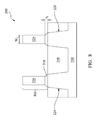
- FIG. 1 is a flow chart of an example method for fabricating a FinFET device in accordance with some embodiments.
- first and second features are formed in direct contact
- additional features may be formed between the first and second features, such that the first and second features may not be in direct contact
- present disclosure may repeat reference numerals and/or letters in the various examples. This repetition is for the purpose of simplicity and clarity and does not in itself dictate a relationship between the various embodiments and/or configurations discussed.
- spatially relative terms such as “beneath,” “below,” “lower,” “above,” “upper” and the like, may be used herein for ease of description to describe one element or feature's relationship to another element(s) or feature(s) as illustrated in the figures.
- the spatially relative terms are intended to encompass different orientations of the device in use or operation in addition to the orientation depicted in the figures.
- the apparatus may be otherwise oriented (rotated 90 degrees or at other orientations) and the spatially relative descriptors used herein may likewise be interpreted accordingly.
- the present disclosure is directed to, but not otherwise limited to, a FinFET device.
- the FinFET device may be a complementary metal-oxide-semiconductor (CMOS) device comprising a P-type metal-oxide-semiconductor (PMOS) FinFET device and an N-type metal-oxide-semiconductor (NMOS) FinFET device.
- CMOS complementary metal-oxide-semiconductor
- PMOS P-type metal-oxide-semiconductor
- NMOS N-type metal-oxide-semiconductor
- FIG. 1 is a flowchart of a method 100 for fabricating a FinFET device 200 according to aspects of the present disclosure.
- FIGS. 2-13 are cross-section views of the FinFET device 200 at fabrication stages constructed according to the method 100 of FIG. 1 .
- the FinFET device 200 is collectively described with reference to FIGS. 1-9 . It is understood that additional steps can be provided before, during, and after the method 100 , and some of the steps described can be replaced or eliminated for other embodiments of the method.
- the method 100 begins at step 102 by forming first fin structures 220 in a substrate 210 .
- the substrate 210 includes silicon.
- the substrate may include germanium, silicon germanium, gallium arsenide or other appropriate semiconductor materials.
- the substrate 210 may include an epitaxial layer.
- the substrate 210 may have an epitaxial layer overlying a bulk semiconductor.
- the substrate 210 may be strained for performance enhancement.
- the epitaxial layer may include a semiconductor material different from those of the bulk semiconductor such as a layer of silicon germanium overlying bulk silicon or a layer of silicon overlying a bulk silicon germanium formed by a process including selective epitaxial growth (SEG).
- SEG selective epitaxial growth
- the substrate 210 may include a semiconductor-on-insulator (SOI) structure such as a buried dielectric layer.
- SOI semiconductor-on-insulator
- the substrate 210 may include a buried dielectric layer such as a buried oxide (BOX) layer, such as that formed by a method referred to as separation by implantation of oxygen (SIMOX) technology, wafer bonding, SEG, or other appropriate methods.
- SOI semiconductor-on-insulator
- BOX buried oxide
- SIMOX separation by implantation of oxygen
- various embodiments may include any of a variety of substrate structures and materials.
- the photolithography exposing process is implemented or replaced by other proper methods such as maskless photolithography, electron-beam writing, direct-writing, and/or ion-beam writing.
- the HM layer is then etched through the pattern photoresist layer to form a patterned HM layer 215 .
- the substrate 210 is then etched through the patterned HM layer to form first fin structures 220 .
- the method 100 proceeds to step 104 by depositing a dielectric layer 240 over the substrate 210 , including filling in spaces between each of first fin structures 220 .
- the dielectric layer 240 between each of the first fin structures 220 serves as an isolation region to separate various device regions in the substrate 210 .
- the dielectric layer 240 may include silicon oxide, silicon nitride, oxynitride, a dielectric material having a dielectric constant (k) lower than thermal silicon oxide (therefore referred to as low-k dielectric material layer), or other suitable dielectric material layer.
- the dielectric layer 240 may include a single layer or multiple layers.
- the dielectric layer 240 may be deposited by chemical vapor deposition (CVD), atomic layer deposition (ALD) or spin-on coating. Additionally, a chemical mechanical polishing (CMP) process may be performed to planarize top surfaces of the dielectric layer 240 (and removed the patterned HM layer as well).
- CVD chemical vapor deposition
- ALD atomic layer deposition
- CMP chemical mechanical polishing
- the method 100 proceeds to step 106 by recessing the first fin structures 220 to form a trench 250 in the dielectric layer 240 .
- a chemical mechanical polishing (CMP) process is performed first to remove excessive the dielectric layer 240 and expose a top surface of the first fin structure 220 .
- the first fin structures 220 is then recessed by a selectively etch, which does not substantially etch the dielectric layer 240 .
- the recessing process may include a selective wet etch or a selective dry etch, or combination thereof.
- a selective wet etching solution includes a tetramethylammonium hydroxide (TMAH), a HF/HNO3/CH3COOH solution, or other suitable solution.
- Dry etching process may include a biased plasma etching process that uses a chlorine-based chemistry, such as such as Cl 2 , CHCl 3 , CCl 4 , and/or BCl 3 .
- the first trench 250 is formed to have the recessed first fin structure 220 at its bottom and the dielectric layer 240 as its sidewalls. In the other words, the recessed first fin structure 220 is exposed in the trench 250 .
- the method 100 proceeds to step 108 by enlarging the trench 250 to form an enlarged trench 260 .
- the enlarged trench 260 has a substantially vertical profile.
- the enlarged trench 260 has a first width w 1 .
- the enlarged trench 260 is formed by etching the dielectric layer 240 through a patterned photoresist layer.
- the etching process includes an anisotropic etch.
- the anisotropic dielectric etch may include a plasma dry etching process using a fluorine-based chemistry, such as CF 4 , SF 6 , CH 2 F 2 , CHF 3 , and/or C 2 F 6 .
- the anisotropic dielectric etch selectively removes the dielectric layer 240 but does not substantially etch the recessed first fin structures 220 .
- the method 100 proceeds to step 110 by conformably depositing a first semiconductor material layer 310 along sidewalls and bottom of the enlarged trench 260 .
- the first semiconductor material layer 310 may include element semiconductor material such as germanium (Ge) or silicon (Si); or compound semiconductor materials, such as gallium arsenide (GaAs), aluminum gallium arsenide (AlGaAs); or semiconductor alloy, such as silicon germanium (SiGe), gallium arsenide phosphide (GaAsP).
- the first semiconductor material layer 310 may be deposited by epitaxial processes including CVD deposition techniques (e.g., vapor-phase epitaxy (VPE) and/or ultra-high vacuum CVD (UHV-CVD)), molecular beam epitaxy, and/or other suitable processes.
- the first semiconductor material layer 310 includes epitaxial Si layer.
- the first semiconductor material layer 310 may be in-situ doped during the epi process.
- the epitaxially grown semiconductor material layer 310 may be doped with boron.
- the epitaxially grown Si layer 310 may be doped with carbon, or phosphorous, or both carbon and phosphorous.
- the first semiconductor layer 310 is not in-situ doped, an implantation process (i.e., a junction implant process) is performed.
- the semiconductor material layer 310 is conformably covers vertical sidewalls of the enlarged trench 260 with a first thickness t 1 and the bottom of the enlarged trench 260 with a second thickness t 2 .
- the second thickness t 2 is thinner than the first thickness t 1 .
- the second thickness t 2 may be substantial same as the first thickness t 1 .
- the method 100 proceeds to step 112 by epitaxially growing a second semiconductor layer 320 from bottom of the remaining enlarged trench 260 .
- the second semiconductor layer 320 may include Ge, Si, GaAs, AlGaAs, SiGe, GaAsP, or other suitable materials.
- the second semiconductor layer 320 includes SiGe.
- the second semiconductor material layer 320 may be epitaxially grown by epitaxial processes including CVD, molecular beam epitaxy, and/or other suitable processes.
- the epitaxially grown second semiconductor material layer 320 fully fills in the remaining enlarged trench 260 .
- Another CMP process is then performed to remove excessive the second and first semiconductor material layer, 310 and 320 , and planarize the top surface of the second and first semiconductor material layer, 310 and 320 , with the top surface of the dielectric layer.
- the method 100 has two paths after step 112 , identified by the suffix “A” and “B,” respectively. Both paths are separately discussed below.
- the method 100 proceeds along path A to step 114 A by recessing the dielectric layer 240 to laterally expose the first semiconductor material layers 310 .
- the dielectric layer 240 is recessed by a proper etching process, such as a selective wet etch, or a selective dry etch, or a combination thereof.
- the etching selectively removes dielectric layer 240 but does not substantially etch the first and second semiconductor material layers, 310 and 320 .
- the recessing processes are controlled to make a top surface 240 a of the recessed dielectric material layer 240 below a bottom surface 310 a of the semiconductor material layers 310 .
- the second semiconductor material layer 320 combining with the remaining the first semiconductor material layer 310 underneath of it forms a second fin structure 410 .
- the second fin structure 410 has the second semiconductor material layer 320 as its upper portion and the first semiconductor material layer 310 as its lower portion.
- the second semiconductor material layer 320 of the upper portion has vertical sidewall profiles, while the first semiconductor material layer 310 of the lower portion has non-vertical sidewall profile, such as it has a wider width at its bottom.
- the non-vertical sidewall profile of the first semiconductor material layer 310 of the lower portion is sloped and/or tapered.
- a width of the upper portion, referred to as a width of the second fin structure 410 is the second width w 2 .
- w 2 w 1 ⁇ (2 ⁇ t 1 ). Therefore a targeted small fin structure width can be achieved by choosing the first width w 1 and the first thickness t 1 .
- a width of the lower portion is equal or less than the second width w 2 .
- the method 100 proceeds along path B to step 114 B (instead of 114 A) by recessing the dielectric layer 240 to laterally expose the second semiconductor material layer 320 .
- the recess is similar in many respects to those discussed above in step 114 A. But the recessing depth is controlled to make a top surface 240 a of the recessed dielectric material layer 240 to be positioned above the bottom surface 310 a of the first semiconductor material layer 310 .
- the top surface 240 a of the recessed dielectric material layer 240 is at the same horizontal level as a top surface 310 b of the first semiconductor material layers 310 that opposes the bottom surface 310 a of the first semiconductor material layer 310 .
- the method 100 proceeds to step 116 B by etching the exposed first semiconductor material layer 310 .
- the step 116 B is similar in many respects to step 116 A.
- a selective etching process is performed and the exposed first semiconductor material layer 310 along sidewalls of the second semiconductor material layer 320 is removed while the second semiconductor material layer 320 remains un-etched.
- the vertical sidewall profile of the second semiconductor material layer 320 remains intact.
- a portion of the first semiconductor material layer 310 which is underneath the second semiconductor material layer 320 remains intact during the recessing process.
- the method 100 proceeds to step 118 B by recessing the dielectric layer 240 further to expose the remaining portion of the first semiconductor material layer 310 underneath the second semiconductor material layer 320 .
- the recessing process is similar in many respects to those discussed above in step 114 B.
- the method 100 proceeds to step 120 B by trimming the remaining portion of the first semiconductor material layer 310 .
- the trimming process is similar in many respects to those discussed above in step 116 A.
- the trimming process is a selective etch, which selective trims the remaining portion of the first semiconductor material layer 310 but does not substantially etch second semiconductor material layer 330 .
- the vertical sidewall profile of the second semiconductor material layer 320 remains intact.
- the second fin structure 410 is formed having the second semiconductor material layer 320 as its upper portion and the first semiconductor material layer 310 as its lower portion.
- the upper portion has vertical sidewall profiles and the second width w 2 .
- the lower portion has non-vertical sidewall profile.
- trimming process such as trimming time, trimming process conditions
- various shapes of the lower portion of the second fin structure 410 can be achieved to meet various device requirements.
- the lower portion of the second fin structure 410 is formed with a keystone shape, which has a wider width at its bottom, as shown in FIG. 12A .
- the lower portion of the second fin structure 410 is formed with a necking-shape, which has a narrowest width in the middle, as shown in FIG. 12B .
- the necking-shape lower portion of the second fin structure 410 is trimmed further to make the second fin structure have a ⁇ -shape 415 , as shown in FIG. 12C .
- a gate-all-around (GAA) gate will be formed over the ⁇ -shape second fin structure 410 , which will be described later.
- the FinFET device 200 may also undergo further CMOS or MOS technology processing to form various features, such as source/drain (S/D) features and gate stacks.
- the second fin structure 410 includes source/drain (S/D) regions and gate regions. S/D features are formed in the S/D regions and gate stacks are formed in the gate regions of the second fin structure 410 .
- a dummy gate stacks are formed first on the substrate 210 and is partially disposed over the second fin structure 410 in the gate regions. The dummy gate stacks will be replaced by the final gate stack at a subsequent stage. Particularly, the dummy gate stacks are to be replaced later by a high-k dielectric layer (HK) and metal gate electrode (MG) after high thermal temperature processes, such as thermal annealing for S/D activation during the sources/drains formation.
- HK high-k dielectric layer
- MG metal gate electrode
- the S/D features are then formed over the S/D regions in the second fin structure 410 .
- the upper portion of the second fin structure 410 in the S/D region is recessed and the S/D features then epitaxially grow on the recessed second fin structure 410 .
- the S/D features include Ge, Si, GaAs, AlGaAs, SiGe, GaAsP, or other suitable material.
- the S/D features may also be doped, such as being in-situ doped during the epitaxial growing processes. Alternatively, the S/D features are not in-situ doped and implantation processes (i.e., a junction implant process) are performed to dope the S/D features.
- an interlayer dielectric (ILD) layer 510 is formed over the substrate 210 between the second fin structures 410 .
- the ILD layer 510 includes silicon oxide, silicon oxynitride, low k dielectric material or other suitable dielectric materials.
- the ILD layer 510 may include a single layer or alternative multiple layers.
- the ILD layer 510 is formed by a suitable technique, such as CVD, ALD and spin-on (SOG). A CMP process may be performed thereafter to remove excessive ILD layer 510 and planarize the top surface of the FinFET device 200 .
- the dummy gate stacks are then replaced by high-k/metal gate (HK/MG) stacks 610 are formed over the substrate 210 , including wrapping over a portion of the second fin structure 410 .
- the HK/MG stacks 610 may include gate dielectric layer and gate electrode on the gate dielectric.
- the gate dielectric layer includes a dielectric material layer having a high dielectric constant (HK dielectric layer-greater than that of the thermal silicon oxide in the present embodiment) and the gate electrode includes metal, metal alloy or metal silicide.
- the formation of the HK/MG stacks 610 includes depositions to form various gate materials and a CMP process to remove the excessive gate materials and planarize the top surface of the FinFET device 200 .
- the gate dielectric layer includes an interfacial layer (IL) 620 deposited by a suitable method, such as atomic layer deposition (ALD), CVD, thermal oxidation or ozone oxidation.
- the IL 620 may include oxide, HfSiO and oxynitride.
- a HK dielectric layer 630 is deposited on the IL 620 by a suitable technique, such as ALD, CVD, metal-organic CVD (MOCVD), physical vapor deposition (PVD), other suitable technique, or a combination thereof.
- the HK dielectric layer 630 may include LaO, AlO, ZrO, TiO, Ta 2 O 5 , Y 2 O 3 , SrTiO 3 (STO), BaTiO 3 (BTO), BaZrO, HfZrO, HfLaO, HfSiO, LaSiO, AlSiO, HfTaO, HfTiO, (Ba,Sr)TiO 3 (BST), Al 2 O 3 , Si 3 N 4 , oxynitride (SiON), or other suitable materials.
- the gate dielectric layers wrap over the second fin structures 410 in the gate region.
- Metal gate (MG) electrodes 640 are formed over the HK dielectric layer 630 .
- the MG electrodes 640 may include a single layer or alternatively a multi-layer structure, such as various combinations of a metal layer with a work function to enhance the device performance (work function metal layer), liner layer, wetting layer, adhesion layer and a conductive layer of metal, metal alloy or metal silicide).
- the MG electrode may include Ti, Ag, Al, TiAlN, TaC, TaCN, TaSiN, Mn, Zr, TiN, TaN, Ru, Mo, Al, WN, Cu, W, any suitable materials or a combination thereof.
- the MG electrode 640 may be formed by ALD, PVD, CVD, or other suitable process.
- a CMP process may be performed to remove excessive MG electrode 640 .
- Subsequent processing may also form various contacts/vias/lines and multilayers interconnect features (e.g., metal layers and interlayer dielectrics) on the substrate 210 , configured to connect the various features or structures of the FinFET device 200 .
- a multilayer interconnection includes vertical interconnects, such as conventional vias or contacts, and horizontal interconnects, such as metal lines.
- the various interconnection features may implement various conductive materials including copper, tungsten, and/or silicide.
- a damascene and/or dual damascene process is used to form a copper related multilayer interconnection structure.
- the present disclosure offers methods and structures for a FinFET device.
- the method employs forming a fin structure with a quite small width without trimming the fin structure itself to improve fin structure shape and critical dimension (CD) control.
- the method also employs forming the fin structure with a desirable vertical profile at its upper portion.
- the method also employs forming various shape of the lower portion of the fin structure to meet various device requirements, such as for a gate-all-around device.
- a method for fabricating a FinFET device includes forming a first fin structure over a substrate, forming a dielectric layer over the first fin structure, forming a trench within the dielectric layer, wherein the first fin structure is exposed in a bottom of the trench, depositing a first semiconductor material layer within the trench, depositing a second semiconductor material layer over the first semiconductor material layer within the trench, recessing the dielectric layer to laterally expose the first semiconductor material layer and etching the exposed first semiconductor material layer to reveal the second semiconductor material layer, wherein at least a portion of the first semiconductor material layer underneath the second semiconductor material layer remains intact.
- a method for fabricating a FinFET device includes A method for fabricating a fin-type field-effect transistor (FinFET) device, the method includes forming a first fin structure, surrounding by a dielectric layer, over a substrate, recessing the first fin structure to form a trench in the dielectric layer, enlarging the trench to have a vertical sidewall profile, depositing conformably a first semiconductor material layer over sidewalls and bottom of the trench, epitaxially growing a second semiconductor material from bottom of the remaining trench, recessing the dielectric layer to laterally expose the first semiconductor material layer, removing the exposed first semiconductor material layer along the sidewall of the second semiconductor material layer, but does not substantially etch the second semiconductor material layer. At least a portion of the first semiconductor material layer underneath the second semiconductor material layer remains intact.
- the method also includes forming a high-k/metal gate over the substrate, including wrapping over the second semiconductor material layer and the remaining first semiconductor material layer underneath the second semiconductor material layer.
- a FinFET device in another embodiment, includes a first fin structure disposed over a substrate, a second fin structure disposed over the first fin structure.
- the second fin structure includes a first semiconductor material layer as its lower portion and a second semiconductor material layer having a vertical sidewall profile as its upper portion.
- the device also includes a high-k/metal gate (HK/MG) disposed over the substrate, including wrapping over the second fin structure.
- HK/MG high-k/metal gate
Abstract
A semiconductor device includes a first fin structure extending from a semiconductor substrate. A second fin structure is disposed over the first fin structure. The second fin structure includes a first layer including a first semiconductor material. The second fin structure further includes a second layer including a second semiconductor material disposed over the first layer. The second layer has a vertical sidewall. The second semiconductor material is different from the first semiconductor material. A gate structure is disposed over the semiconductor substrate and wraps around the first and second layers of the second fin structure.
Description
The present application is a continuation application of U.S. patent application Ser. No. 14/318,140, filed Jun. 27, 2014, now U.S. Pat. No. 9,406,782, entitled “STRUCTURE AND METHOD FOR FINFET DEVICE”, which is hereby incorporated by reference in its entirety.
The semiconductor integrated circuit (IC) industry has experienced exponential growth. Technological advances in IC materials and design have produced generations of ICs where each generation has smaller and more complex circuits than the previous generation. In the course of IC evolution, functional density (i.e., the number of interconnected devices per chip area) has generally increased while geometry size (i.e., the smallest component (or line) that can be created using a fabrication process) has decreased. This scaling down process generally provides benefits by increasing production efficiency and lowering associated costs.
Such scaling down has also increased the complexity of processing and manufacturing ICs and, for these advances to be realized, similar developments in IC processing and manufacturing are needed. For example, a three dimensional transistor, such as a fin-type field-effect transistor (FinFET), has been introduced to replace a planar transistor. Although existing FinFET devices and methods of fabricating FinFET devices have been generally adequate for their intended purposes, they have not been entirely satisfactory in all respects. It is desired to have improvements in this area.
Aspects of the present disclosure are best understood from the following detailed description when read with the accompanying figures. It is noted that, in accordance with the standard practice in the industry, various features are not drawn to scale. In fact, the dimensions of the various features may be arbitrarily increased or reduced for clarity of discussion.
The following disclosure provides many different embodiments, or examples, for implementing different features of the invention. Specific examples of components and arrangements are described below to simplify the present disclosure. These are, of course, merely examples and are not intended to be limiting. For example, the formation of a first feature over or on a second feature in the description that follows may include embodiments in which the first and second features are formed in direct contact, and may also include embodiments in which additional features may be formed between the first and second features, such that the first and second features may not be in direct contact. In addition, the present disclosure may repeat reference numerals and/or letters in the various examples. This repetition is for the purpose of simplicity and clarity and does not in itself dictate a relationship between the various embodiments and/or configurations discussed.
Further, spatially relative terms, such as “beneath,” “below,” “lower,” “above,” “upper” and the like, may be used herein for ease of description to describe one element or feature's relationship to another element(s) or feature(s) as illustrated in the figures. The spatially relative terms are intended to encompass different orientations of the device in use or operation in addition to the orientation depicted in the figures. The apparatus may be otherwise oriented (rotated 90 degrees or at other orientations) and the spatially relative descriptors used herein may likewise be interpreted accordingly.
The present disclosure is directed to, but not otherwise limited to, a FinFET device. The FinFET device, for example, may be a complementary metal-oxide-semiconductor (CMOS) device comprising a P-type metal-oxide-semiconductor (PMOS) FinFET device and an N-type metal-oxide-semiconductor (NMOS) FinFET device. The following disclosure will continue with a FinFET example to illustrate various embodiments of the present invention. It is understood, however, that the application should not be limited to a particular type of device, except as specifically claimed.
Referring to FIGS. 1 and 2 , the method 100 begins at step 102 by forming first fin structures 220 in a substrate 210. The substrate 210 includes silicon. In another embodiment, the substrate may include germanium, silicon germanium, gallium arsenide or other appropriate semiconductor materials. Alternatively and for some embodiments, the substrate 210 may include an epitaxial layer. For example, the substrate 210 may have an epitaxial layer overlying a bulk semiconductor. Further, the substrate 210 may be strained for performance enhancement. For example, the epitaxial layer may include a semiconductor material different from those of the bulk semiconductor such as a layer of silicon germanium overlying bulk silicon or a layer of silicon overlying a bulk silicon germanium formed by a process including selective epitaxial growth (SEG). Furthermore, the substrate 210 may include a semiconductor-on-insulator (SOI) structure such as a buried dielectric layer. Also alternatively, the substrate 210 may include a buried dielectric layer such as a buried oxide (BOX) layer, such as that formed by a method referred to as separation by implantation of oxygen (SIMOX) technology, wafer bonding, SEG, or other appropriate methods. In fact various embodiments may include any of a variety of substrate structures and materials.
The first fin structures 220 may be formed by one or more procedures such as deposition, lithography and etching. In one embodiment, a hard mask (HM) layer is formed over the substrate 210. The HM layer may include may include silicon nitride, silicon oxide, silicon carbide, titanium oxide, titanium nitride, tantalum oxide, tantalum nitride, or any suitable materials. A patterned photoresist layer is then formed over the HM layer to define first fin structures 220. Generally, a patterning process may include photoresist coating (e.g., spin-on coating), exposing, developing the photoresist, other suitable processes, or combinations thereof. Alternatively, the photolithography exposing process is implemented or replaced by other proper methods such as maskless photolithography, electron-beam writing, direct-writing, and/or ion-beam writing. The HM layer is then etched through the pattern photoresist layer to form a patterned HM layer 215. The substrate 210 is then etched through the patterned HM layer to form first fin structures 220.
The substrate 210 may be etched by various methods, including a dry etch, a wet etch, or a combination of thereof. In one embodiment, the wet etching solution includes a tetramethylammonium hydroxide (TMAH), a HF/HNO3/CH3COOH solution, or other suitable solution. The respective etch process may be tuned with various etching parameters, such as etchant used, etching temperature, etching solution concentration, etching pressure, source power, RF bias voltage, RF bias power, etchant flow rate, and/or other suitable parameters. Dry etching processes may include a biased plasma etching process that uses a chlorine-based chemistry. Other dry etchant gasses include CF4, NF3, SF6, and He. Dry etching may also be performed anisotropically using such mechanism as DRIE (deep reactive-ion etching).
Referring also to FIGS. 1 and 2 , the method 100 proceeds to step 104 by depositing a dielectric layer 240 over the substrate 210, including filling in spaces between each of first fin structures 220. In one embodiment, the dielectric layer 240 between each of the first fin structures 220 serves as an isolation region to separate various device regions in the substrate 210. The dielectric layer 240 may include silicon oxide, silicon nitride, oxynitride, a dielectric material having a dielectric constant (k) lower than thermal silicon oxide (therefore referred to as low-k dielectric material layer), or other suitable dielectric material layer. The dielectric layer 240 may include a single layer or multiple layers. The dielectric layer 240 may be deposited by chemical vapor deposition (CVD), atomic layer deposition (ALD) or spin-on coating. Additionally, a chemical mechanical polishing (CMP) process may be performed to planarize top surfaces of the dielectric layer 240 (and removed the patterned HM layer as well).
Referring to FIGS. 1 and 3 , the method 100 proceeds to step 106 by recessing the first fin structures 220 to form a trench 250 in the dielectric layer 240. In one embodiment, a chemical mechanical polishing (CMP) process is performed first to remove excessive the dielectric layer 240 and expose a top surface of the first fin structure 220. The first fin structures 220 is then recessed by a selectively etch, which does not substantially etch the dielectric layer 240. The recessing process may include a selective wet etch or a selective dry etch, or combination thereof. In one embodiment, a selective wet etching solution includes a tetramethylammonium hydroxide (TMAH), a HF/HNO3/CH3COOH solution, or other suitable solution. Dry etching process may include a biased plasma etching process that uses a chlorine-based chemistry, such as such as Cl2, CHCl3, CCl4, and/or BCl3. The first trench 250 is formed to have the recessed first fin structure 220 at its bottom and the dielectric layer 240 as its sidewalls. In the other words, the recessed first fin structure 220 is exposed in the trench 250.
Referring to FIGS. 1 and 4 , the method 100 proceeds to step 108 by enlarging the trench 250 to form an enlarged trench 260. In the present embodiment, the enlarged trench 260 has a substantially vertical profile. The enlarged trench 260 has a first width w1. In one embodiment, the enlarged trench 260 is formed by etching the dielectric layer 240 through a patterned photoresist layer. The etching process includes an anisotropic etch. The anisotropic dielectric etch may include a plasma dry etching process using a fluorine-based chemistry, such as CF4, SF6, CH2F2, CHF3, and/or C2F6. The anisotropic dielectric etch selectively removes the dielectric layer 240 but does not substantially etch the recessed first fin structures 220.
Referring to FIGS. 1 and 5 , the method 100 proceeds to step 110 by conformably depositing a first semiconductor material layer 310 along sidewalls and bottom of the enlarged trench 260. The first semiconductor material layer 310 may include element semiconductor material such as germanium (Ge) or silicon (Si); or compound semiconductor materials, such as gallium arsenide (GaAs), aluminum gallium arsenide (AlGaAs); or semiconductor alloy, such as silicon germanium (SiGe), gallium arsenide phosphide (GaAsP). The first semiconductor material layer 310 may be deposited by epitaxial processes including CVD deposition techniques (e.g., vapor-phase epitaxy (VPE) and/or ultra-high vacuum CVD (UHV-CVD)), molecular beam epitaxy, and/or other suitable processes. In present embodiment, the first semiconductor material layer 310 includes epitaxial Si layer. The first semiconductor material layer 310 may be in-situ doped during the epi process. For example, the epitaxially grown semiconductor material layer 310 may be doped with boron. For another example, the epitaxially grown Si layer 310 may be doped with carbon, or phosphorous, or both carbon and phosphorous. In another embodiment, the first semiconductor layer 310 is not in-situ doped, an implantation process (i.e., a junction implant process) is performed.
In the present embodiment, the semiconductor material layer 310 is conformably covers vertical sidewalls of the enlarged trench 260 with a first thickness t1 and the bottom of the enlarged trench 260 with a second thickness t2. In one embodiment, the second thickness t2 is thinner than the first thickness t1. In another embodiment, the second thickness t2 may be substantial same as the first thickness t1. After deposition the first semiconductor material layer 310, the first width w1 of the enlarged trench 260 is reduced to a second width w2, which is w2=w1−(2×t1). By choosing the first width w1 and the thickness t, the second width w2 is a targeted fin width, which will be described later.
Referring to FIGS. 1 and 6 , the method 100 proceeds to step 112 by epitaxially growing a second semiconductor layer 320 from bottom of the remaining enlarged trench 260. The second semiconductor layer 320 may include Ge, Si, GaAs, AlGaAs, SiGe, GaAsP, or other suitable materials. In the present embodiment, the second semiconductor layer 320 includes SiGe. The second semiconductor material layer 320 may be epitaxially grown by epitaxial processes including CVD, molecular beam epitaxy, and/or other suitable processes. The epitaxially grown second semiconductor material layer 320 fully fills in the remaining enlarged trench 260. Another CMP process is then performed to remove excessive the second and first semiconductor material layer, 310 and 320, and planarize the top surface of the second and first semiconductor material layer, 310 and 320, with the top surface of the dielectric layer.
The method 100 has two paths after step 112, identified by the suffix “A” and “B,” respectively. Both paths are separately discussed below.
Referring to FIGS. 1 and 7 , the method 100 proceeds along path A to step 114A by recessing the dielectric layer 240 to laterally expose the first semiconductor material layers 310. The dielectric layer 240 is recessed by a proper etching process, such as a selective wet etch, or a selective dry etch, or a combination thereof. The etching selectively removes dielectric layer 240 but does not substantially etch the first and second semiconductor material layers, 310 and 320. In present embodiment, the recessing processes are controlled to make a top surface 240 a of the recessed dielectric material layer 240 below a bottom surface 310 a of the semiconductor material layers 310.
Referring to FIGS. 1 and 8 , the method 100 proceeds to step 116A by etching the exposed first semiconductor material layer 310. In the present embodiment, the exposed first semiconductor material layer 310 is etched by a selective etch such that the etching process does not substantially etch the second semiconductor material layer 320. Thus, the vertical sidewall profile of the second semiconductor material layer 320 remains intact. In one embodiment, the Si layer 310 is etched by a wet etch solution of NH4OH:H2O2, with a high selectivity with respect to the SiGe layer 320. In another embodiment, the Si layer 310 is etched by a wet etch solution of TMAH. The etching process is controlled that the exposed first semiconductor material layer 310 along sidewalls of the second semiconductor material layer 320 are fully removed while at least a portion of the first semiconductor material layer 310 underneath the second semiconductor material layer 320 partially remains intact.
In the present embodiment, the second semiconductor material layer 320 combining with the remaining the first semiconductor material layer 310 underneath of it forms a second fin structure 410. Thus, the second fin structure 410 has the second semiconductor material layer 320 as its upper portion and the first semiconductor material layer 310 as its lower portion. The second semiconductor material layer 320 of the upper portion has vertical sidewall profiles, while the first semiconductor material layer 310 of the lower portion has non-vertical sidewall profile, such as it has a wider width at its bottom. Here, the non-vertical sidewall profile of the first semiconductor material layer 310 of the lower portion is sloped and/or tapered. A width of the upper portion, referred to as a width of the second fin structure 410, is the second width w2. As mentioned previously, w2=w1−(2×t1). Therefore a targeted small fin structure width can be achieved by choosing the first width w1 and the first thickness t1. A width of the lower portion is equal or less than the second width w2.
Referring to FIGS. 1 and 9 , alternatively, after completing the step 112, the method 100 proceeds along path B to step 114B (instead of 114A) by recessing the dielectric layer 240 to laterally expose the second semiconductor material layer 320. The recess is similar in many respects to those discussed above in step 114A. But the recessing depth is controlled to make a top surface 240 a of the recessed dielectric material layer 240 to be positioned above the bottom surface 310 a of the first semiconductor material layer 310. Here, the top surface 240 a of the recessed dielectric material layer 240 is at the same horizontal level as a top surface 310 b of the first semiconductor material layers 310 that opposes the bottom surface 310 a of the first semiconductor material layer 310.
Referring to FIGS. 1 and 10 , the method 100 proceeds to step 116B by etching the exposed first semiconductor material layer 310. The step 116B is similar in many respects to step 116A. A selective etching process is performed and the exposed first semiconductor material layer 310 along sidewalls of the second semiconductor material layer 320 is removed while the second semiconductor material layer 320 remains un-etched. Thus, the vertical sidewall profile of the second semiconductor material layer 320 remains intact. Also, with an adequate selective etching of the first semiconductor material layer 310 with respect to the second semiconductor material layer 320 and the dielectric layer 240, a portion of the first semiconductor material layer 310, which is underneath the second semiconductor material layer 320 remains intact during the recessing process.
Referring to FIGS. 1 and 11 , the method 100 proceeds to step 118B by recessing the dielectric layer 240 further to expose the remaining portion of the first semiconductor material layer 310 underneath the second semiconductor material layer 320. The recessing process is similar in many respects to those discussed above in step 114B.
Referring to FIGS. 1 and 12A-12C , the method 100 proceeds to step 120B by trimming the remaining portion of the first semiconductor material layer 310. The trimming process is similar in many respects to those discussed above in step 116A. In the present embodiment, the trimming process is a selective etch, which selective trims the remaining portion of the first semiconductor material layer 310 but does not substantially etch second semiconductor material layer 330. Thus, the vertical sidewall profile of the second semiconductor material layer 320 remains intact.
As mentioned in step 116A, the second fin structure 410 is formed having the second semiconductor material layer 320 as its upper portion and the first semiconductor material layer 310 as its lower portion. The upper portion has vertical sidewall profiles and the second width w2. The lower portion has non-vertical sidewall profile. By controlling trimming process, such as trimming time, trimming process conditions, various shapes of the lower portion of the second fin structure 410 can be achieved to meet various device requirements. In one embodiment, the lower portion of the second fin structure 410 is formed with a keystone shape, which has a wider width at its bottom, as shown in FIG. 12A . In another embodiment, with a longer trimming time, the lower portion of the second fin structure 410 is formed with a necking-shape, which has a narrowest width in the middle, as shown in FIG. 12B . In yet another embodiment, the necking-shape lower portion of the second fin structure 410 is trimmed further to make the second fin structure have a Ω-shape 415, as shown in FIG. 12C . A gate-all-around (GAA) gate will be formed over the Ω-shape second fin structure 410, which will be described later.
The FinFET device 200 may also undergo further CMOS or MOS technology processing to form various features, such as source/drain (S/D) features and gate stacks. The second fin structure 410 includes source/drain (S/D) regions and gate regions. S/D features are formed in the S/D regions and gate stacks are formed in the gate regions of the second fin structure 410. In one embodiment, a dummy gate stacks are formed first on the substrate 210 and is partially disposed over the second fin structure 410 in the gate regions. The dummy gate stacks will be replaced by the final gate stack at a subsequent stage. Particularly, the dummy gate stacks are to be replaced later by a high-k dielectric layer (HK) and metal gate electrode (MG) after high thermal temperature processes, such as thermal annealing for S/D activation during the sources/drains formation.
The S/D features are then formed over the S/D regions in the second fin structure 410. In one embodiment, the upper portion of the second fin structure 410 in the S/D region is recessed and the S/D features then epitaxially grow on the recessed second fin structure 410. The S/D features include Ge, Si, GaAs, AlGaAs, SiGe, GaAsP, or other suitable material. The S/D features may also be doped, such as being in-situ doped during the epitaxial growing processes. Alternatively, the S/D features are not in-situ doped and implantation processes (i.e., a junction implant process) are performed to dope the S/D features.
The following descriptions will be directed to the embodiment of FIG. 12C , for the sake of example. It is understood that similar processes can be implemented on embodiments of FIGS. 8 and 12A-12B .
Now referring to FIG. 13 , an interlayer dielectric (ILD) layer 510 is formed over the substrate 210 between the second fin structures 410. The ILD layer 510 includes silicon oxide, silicon oxynitride, low k dielectric material or other suitable dielectric materials. The ILD layer 510 may include a single layer or alternative multiple layers. The ILD layer 510 is formed by a suitable technique, such as CVD, ALD and spin-on (SOG). A CMP process may be performed thereafter to remove excessive ILD layer 510 and planarize the top surface of the FinFET device 200.
The dummy gate stacks are then replaced by high-k/metal gate (HK/MG) stacks 610 are formed over the substrate 210, including wrapping over a portion of the second fin structure 410. The HK/MG stacks 610 may include gate dielectric layer and gate electrode on the gate dielectric. In one embodiment, the gate dielectric layer includes a dielectric material layer having a high dielectric constant (HK dielectric layer-greater than that of the thermal silicon oxide in the present embodiment) and the gate electrode includes metal, metal alloy or metal silicide. The formation of the HK/MG stacks 610 includes depositions to form various gate materials and a CMP process to remove the excessive gate materials and planarize the top surface of the FinFET device 200.
In one embodiment, the gate dielectric layer includes an interfacial layer (IL) 620 deposited by a suitable method, such as atomic layer deposition (ALD), CVD, thermal oxidation or ozone oxidation. The IL 620 may include oxide, HfSiO and oxynitride. A HK dielectric layer 630 is deposited on the IL 620 by a suitable technique, such as ALD, CVD, metal-organic CVD (MOCVD), physical vapor deposition (PVD), other suitable technique, or a combination thereof. The HK dielectric layer 630 may include LaO, AlO, ZrO, TiO, Ta2O5, Y2O3, SrTiO3 (STO), BaTiO3 (BTO), BaZrO, HfZrO, HfLaO, HfSiO, LaSiO, AlSiO, HfTaO, HfTiO, (Ba,Sr)TiO3 (BST), Al2O3, Si3N4, oxynitride (SiON), or other suitable materials. The gate dielectric layers wrap over the second fin structures 410 in the gate region.
Metal gate (MG) electrodes 640 are formed over the HK dielectric layer 630. The MG electrodes 640 may include a single layer or alternatively a multi-layer structure, such as various combinations of a metal layer with a work function to enhance the device performance (work function metal layer), liner layer, wetting layer, adhesion layer and a conductive layer of metal, metal alloy or metal silicide). The MG electrode may include Ti, Ag, Al, TiAlN, TaC, TaCN, TaSiN, Mn, Zr, TiN, TaN, Ru, Mo, Al, WN, Cu, W, any suitable materials or a combination thereof. The MG electrode 640 may be formed by ALD, PVD, CVD, or other suitable process. A CMP process may be performed to remove excessive MG electrode 640.
Subsequent processing may also form various contacts/vias/lines and multilayers interconnect features (e.g., metal layers and interlayer dielectrics) on the substrate 210, configured to connect the various features or structures of the FinFET device 200. For example, a multilayer interconnection includes vertical interconnects, such as conventional vias or contacts, and horizontal interconnects, such as metal lines. The various interconnection features may implement various conductive materials including copper, tungsten, and/or silicide. In one example, a damascene and/or dual damascene process is used to form a copper related multilayer interconnection structure.
Additional steps can be provided before, during, and after the method 100, and some of the steps described can be replaced or eliminated for other embodiments of the method.
Based on the above, the present disclosure offers methods and structures for a FinFET device. The method employs forming a fin structure with a quite small width without trimming the fin structure itself to improve fin structure shape and critical dimension (CD) control. The method also employs forming the fin structure with a desirable vertical profile at its upper portion. The method also employs forming various shape of the lower portion of the fin structure to meet various device requirements, such as for a gate-all-around device.
The present disclosure provides many different embodiments of fabricating a FinFET device that provide one or more improvements over the prior art. In one embodiment, a method for fabricating a FinFET device includes forming a first fin structure over a substrate, forming a dielectric layer over the first fin structure, forming a trench within the dielectric layer, wherein the first fin structure is exposed in a bottom of the trench, depositing a first semiconductor material layer within the trench, depositing a second semiconductor material layer over the first semiconductor material layer within the trench, recessing the dielectric layer to laterally expose the first semiconductor material layer and etching the exposed first semiconductor material layer to reveal the second semiconductor material layer, wherein at least a portion of the first semiconductor material layer underneath the second semiconductor material layer remains intact.
In yet another embodiment, a method for fabricating a FinFET device includes A method for fabricating a fin-type field-effect transistor (FinFET) device, the method includes forming a first fin structure, surrounding by a dielectric layer, over a substrate, recessing the first fin structure to form a trench in the dielectric layer, enlarging the trench to have a vertical sidewall profile, depositing conformably a first semiconductor material layer over sidewalls and bottom of the trench, epitaxially growing a second semiconductor material from bottom of the remaining trench, recessing the dielectric layer to laterally expose the first semiconductor material layer, removing the exposed first semiconductor material layer along the sidewall of the second semiconductor material layer, but does not substantially etch the second semiconductor material layer. At least a portion of the first semiconductor material layer underneath the second semiconductor material layer remains intact. The method also includes forming a high-k/metal gate over the substrate, including wrapping over the second semiconductor material layer and the remaining first semiconductor material layer underneath the second semiconductor material layer.
In another embodiment, a FinFET device includes a first fin structure disposed over a substrate, a second fin structure disposed over the first fin structure. The second fin structure includes a first semiconductor material layer as its lower portion and a second semiconductor material layer having a vertical sidewall profile as its upper portion. The device also includes a high-k/metal gate (HK/MG) disposed over the substrate, including wrapping over the second fin structure.
The foregoing outlines features of several embodiments so that those skilled in the art may better understand the aspects of the present disclosure. Those skilled in the art should appreciate that they may readily use the present disclosure as a basis for designing or modifying other processes and structures for carrying out the same purposes and/or achieving the same advantages of the embodiments introduced herein. Those skilled in the art should also realize that such equivalent constructions do not depart from the spirit and scope of the present disclosure, and that they may make various changes, substitutions, and alterations herein without departing from the spirit and scope of the present disclosure.
Claims (20)
1. A semiconductor device comprising:
a first fin structure extending from a semiconductor substrate;
a second fin structure disposed over the first fin structure, the second fin structure including:
a first layer including a first semiconductor material; and
a second layer including a second semiconductor material disposed over the first layer, the second layer having a vertical sidewall, wherein the second semiconductor material is different from the first semiconductor material; and
a gate structure disposed over the semiconductor substrate, the gate structure wrapping around the first and second layers of the second fin structure.
2. The semiconductor device of claim 1 , wherein the first semiconductor material includes silicon and the second semiconductor material includes silicon germanium.
3. The semiconductor device of claim 1 , wherein the first layer has a tapered sidewall.
4. The semiconductor device of claim 1 , wherein the first layer provides a first width of the second fin structure, and the second layer provides a second width of the second fin structure, and
wherein the first width is less than the second width.
5. The semiconductor device of claim 4 , wherein a top portion of the first layer provides the first width of the second fin structure,
wherein a bottom portion of the first layer provides a third width of the second fin structure, and
wherein the third width is less than the second width.
6. The semiconductor device of claim 5 , wherein the first width is less than the third width.
7. The semiconductor device of claim 5 , wherein the first width is greater than the third width.
8. A semiconductor device comprising:
a first fin structure extending from a substrate;
a second fin structure disposed over the first fin structure, the second fin structure including:
a lower portion including a first semiconductor material, wherein the lower portion has a tapered sidewall; and
an upper portion including a second semiconductor material, wherein the second semiconductor material is different from the first semiconductor material; and
a gate structure disposed over the first and second fin structures.
9. The semiconductor device of claim 8 , wherein the first semiconductor material is silicon and the second semiconductor material is silicon germanium.
10. The semiconductor device of claim 8 , wherein the gate structure includes:
a gate dielectric layer wrapping around the second fin structure; and
a metal gate electrode wrapping around the gate dielectric layer.
11. The semiconductor device of claim 10 , wherein a portion of the metal gate electrode is disposed vertically under a bottom surface of the upper portion of the second fin structure.
12. The semiconductor device of claim 11 , wherein the portion of the metal gate electrode is disposed vertically over a top surface of the first fin structure.
13. The semiconductor device of claim 8 , wherein the upper portion of the second fin structure has a vertical profile.
14. The semiconductor device of claim 13 , wherein a widest width of the lower portion is less than a width of the upper portion.
15. The semiconductor device of claim 13 , wherein a widest width of the lower portion is greater than a width of the upper portion.
16. A semiconductor device comprising:
a first fin structure extending from a substrate;
a second fin structure disposed over the first fin structure, the second fin structure including:
a lower portion including a first semiconductor material, wherein the lower portion has a tapered sidewall; and
an upper portion including a second semiconductor material, wherein the second semiconductor material is different from the first semiconductor material; and
a gate structure disposed over the substrate, wherein a portion of the gate structure is disposed vertically under a bottom surface of the upper portion of the second fin structure.
17. The semiconductor device of claim 16 , wherein the first semiconductor material is silicon and the second semiconductor material is silicon germanium.
18. The semiconductor device of claim 16 , wherein the lower portion provides a first width of the second fin structure, and the upper portion provides a second width of the second fin structure, and
wherein the first width is less than the second width.
19. The semiconductor device of claim 16 , wherein the portion of the gate structure includes a metal gate electrode disposed vertically under the bottom surface of the upper portion of the second fin structure.
20. The semiconductor device of claim 19 , wherein the metal gate electrode is disposed vertically over a top surface of the first fin structure.
Priority Applications (1)
| Application Number | Priority Date | Filing Date | Title |
|---|---|---|---|
| US15/225,480 US10269792B2 (en) | 2014-06-27 | 2016-08-01 | Structure and method for FINFET device |
Applications Claiming Priority (2)
| Application Number | Priority Date | Filing Date | Title |
|---|---|---|---|
| US14/318,140 US9406782B2 (en) | 2014-06-27 | 2014-06-27 | Structure and method for FinFET device |
| US15/225,480 US10269792B2 (en) | 2014-06-27 | 2016-08-01 | Structure and method for FINFET device |
Related Parent Applications (1)
| Application Number | Title | Priority Date | Filing Date |
|---|---|---|---|
| US14/318,140 Continuation US9406782B2 (en) | 2014-06-27 | 2014-06-27 | Structure and method for FinFET device |
Publications (2)
| Publication Number | Publication Date |
|---|---|
| US20160343710A1 US20160343710A1 (en) | 2016-11-24 |
| US10269792B2 true US10269792B2 (en) | 2019-04-23 |
Family
ID=54931410
Family Applications (2)
| Application Number | Title | Priority Date | Filing Date |
|---|---|---|---|
| US14/318,140 Active 2034-08-16 US9406782B2 (en) | 2014-06-27 | 2014-06-27 | Structure and method for FinFET device |
| US15/225,480 Active 2035-06-12 US10269792B2 (en) | 2014-06-27 | 2016-08-01 | Structure and method for FINFET device |
Family Applications Before (1)
| Application Number | Title | Priority Date | Filing Date |
|---|---|---|---|
| US14/318,140 Active 2034-08-16 US9406782B2 (en) | 2014-06-27 | 2014-06-27 | Structure and method for FinFET device |
Country Status (3)
| Country | Link |
|---|---|
| US (2) | US9406782B2 (en) |
| KR (1) | KR101706432B1 (en) |
| CN (1) | CN105280558B (en) |
Families Citing this family (7)
| Publication number | Priority date | Publication date | Assignee | Title |
|---|---|---|---|---|
| US11121238B2 (en) * | 2018-11-29 | 2021-09-14 | Taiwan Semiconductor Manufacturing Co., Ltd. | Semiconductor device and manufacturing method thereof |
| US11195759B2 (en) * | 2018-11-30 | 2021-12-07 | Taiwan Semiconductor Manufacturing Company Limited | Semiconductor arrangement and method for making |
| CN111834208A (en) * | 2019-04-16 | 2020-10-27 | 中芯国际集成电路制造(上海)有限公司 | Metal gate forming method and semiconductor device |
| KR20210018573A (en) | 2019-08-05 | 2021-02-18 | 삼성전자주식회사 | Semiconductor device including active region and gate structure |
| US11901457B2 (en) * | 2019-12-02 | 2024-02-13 | Intel Corporation | Fin shaping and integrated circuit structures resulting therefrom |
| US20230268345A1 (en) * | 2022-02-22 | 2023-08-24 | International Business Machines Corporation | Integration of stacked nanosheets and finfet |
| CN115863252B (en) * | 2023-01-29 | 2023-05-23 | 合肥晶合集成电路股份有限公司 | Preparation method of semiconductor structure |
Citations (16)
| Publication number | Priority date | Publication date | Assignee | Title |
|---|---|---|---|---|
| US8395195B2 (en) | 2010-02-09 | 2013-03-12 | Taiwan Semiconductor Manufacturing Company, Ltd. | Bottom-notched SiGe FinFET formation using condensation |
| US8614127B1 (en) | 2013-01-18 | 2013-12-24 | Taiwan Semiconductor Manufacturing Company, Ltd. | Method of making a FinFET device |
| US8618556B2 (en) | 2011-06-30 | 2013-12-31 | Taiwan Semiconductor Manufacturing Company, Ltd. | FinFET design and method of fabricating same |
| US20140197458A1 (en) | 2013-01-14 | 2014-07-17 | Taiwan Semiconductor Manufacturing Company, Ltd. | FinFET Device and Method of Fabricating Same |
| US8901607B2 (en) | 2013-01-14 | 2014-12-02 | Taiwan Semiconductor Manufacturing Company, Ltd. | Semiconductor device and fabricating the same |
| US20150179768A1 (en) | 2013-12-20 | 2015-06-25 | Taiwan Semiconductor Manufacturing Company, Ltd. | Fin Structure of Semiconductor Device |
| US9093302B2 (en) | 2013-11-13 | 2015-07-28 | Globalfoundries Inc. | Methods of forming substantially self-aligned isolation regions on FinFET semiconductor devices and the resulting devices |
| US20150263159A1 (en) | 2014-03-17 | 2015-09-17 | Taiwan Semiconductor Manufacturing Company, Ltd. | FINFET Structure and Method for Fabricating the Same |
| US9142676B2 (en) | 2013-12-30 | 2015-09-22 | Taiwan Semiconductor Manufacturing Company, Ltd. | Semiconductor liner of semiconductor device |
| US9142651B1 (en) | 2014-03-26 | 2015-09-22 | Globalfoundries Inc. | Methods of forming a FinFET semiconductor device so as to reduce punch-through leakage currents and the resulting device |
| US9214553B2 (en) | 2014-03-07 | 2015-12-15 | Globalfoundries Inc. | Methods of forming stressed channel regions for a FinFET semiconductor device and the resulting device |
| US9236478B2 (en) * | 2013-03-01 | 2016-01-12 | Stmicroelectronics Sa | Method for manufacturing a fin MOS transistor |
| US9306069B2 (en) | 2013-09-11 | 2016-04-05 | Taiwan Semiconductor Manufacturing Company, Ltd. | Isolation structure of fin field effect transistor |
| US9318606B2 (en) | 2013-01-14 | 2016-04-19 | Taiwan Semiconductor Manufacturing Company, Ltd. | FinFET device and method of fabricating same |
| US9472446B2 (en) * | 2014-06-18 | 2016-10-18 | Globalfoundries Inc. | Methods of forming a FinFET semiconductor device with a unique gate configuration, and the resulting FinFET device |
| US9559181B2 (en) * | 2013-11-26 | 2017-01-31 | Taiwan Semiconductor Manufacturing Company, Ltd. | Structure and method for FinFET device with buried sige oxide |
Family Cites Families (3)
| Publication number | Priority date | Publication date | Assignee | Title |
|---|---|---|---|---|
| US7485520B2 (en) * | 2007-07-05 | 2009-02-03 | International Business Machines Corporation | Method of manufacturing a body-contacted finfet |
| US8901537B2 (en) * | 2010-12-21 | 2014-12-02 | Intel Corporation | Transistors with high concentration of boron doped germanium |
| US9318431B2 (en) * | 2011-11-04 | 2016-04-19 | Taiwan Semiconductor Manufacturing Company, Ltd. | Integrated circuit having a MOM capacitor and method of making same |
-
2014
- 2014-06-27 US US14/318,140 patent/US9406782B2/en active Active
- 2014-12-23 KR KR1020140186815A patent/KR101706432B1/en active IP Right Grant
-
2015
- 2015-05-29 CN CN201510288647.3A patent/CN105280558B/en active Active
-
2016
- 2016-08-01 US US15/225,480 patent/US10269792B2/en active Active
Patent Citations (16)
| Publication number | Priority date | Publication date | Assignee | Title |
|---|---|---|---|---|
| US8395195B2 (en) | 2010-02-09 | 2013-03-12 | Taiwan Semiconductor Manufacturing Company, Ltd. | Bottom-notched SiGe FinFET formation using condensation |
| US8618556B2 (en) | 2011-06-30 | 2013-12-31 | Taiwan Semiconductor Manufacturing Company, Ltd. | FinFET design and method of fabricating same |
| US20140197458A1 (en) | 2013-01-14 | 2014-07-17 | Taiwan Semiconductor Manufacturing Company, Ltd. | FinFET Device and Method of Fabricating Same |
| US8901607B2 (en) | 2013-01-14 | 2014-12-02 | Taiwan Semiconductor Manufacturing Company, Ltd. | Semiconductor device and fabricating the same |
| US9318606B2 (en) | 2013-01-14 | 2016-04-19 | Taiwan Semiconductor Manufacturing Company, Ltd. | FinFET device and method of fabricating same |
| US8614127B1 (en) | 2013-01-18 | 2013-12-24 | Taiwan Semiconductor Manufacturing Company, Ltd. | Method of making a FinFET device |
| US9236478B2 (en) * | 2013-03-01 | 2016-01-12 | Stmicroelectronics Sa | Method for manufacturing a fin MOS transistor |
| US9306069B2 (en) | 2013-09-11 | 2016-04-05 | Taiwan Semiconductor Manufacturing Company, Ltd. | Isolation structure of fin field effect transistor |
| US9093302B2 (en) | 2013-11-13 | 2015-07-28 | Globalfoundries Inc. | Methods of forming substantially self-aligned isolation regions on FinFET semiconductor devices and the resulting devices |
| US9559181B2 (en) * | 2013-11-26 | 2017-01-31 | Taiwan Semiconductor Manufacturing Company, Ltd. | Structure and method for FinFET device with buried sige oxide |
| US20150179768A1 (en) | 2013-12-20 | 2015-06-25 | Taiwan Semiconductor Manufacturing Company, Ltd. | Fin Structure of Semiconductor Device |
| US9142676B2 (en) | 2013-12-30 | 2015-09-22 | Taiwan Semiconductor Manufacturing Company, Ltd. | Semiconductor liner of semiconductor device |
| US9214553B2 (en) | 2014-03-07 | 2015-12-15 | Globalfoundries Inc. | Methods of forming stressed channel regions for a FinFET semiconductor device and the resulting device |
| US20150263159A1 (en) | 2014-03-17 | 2015-09-17 | Taiwan Semiconductor Manufacturing Company, Ltd. | FINFET Structure and Method for Fabricating the Same |
| US9142651B1 (en) | 2014-03-26 | 2015-09-22 | Globalfoundries Inc. | Methods of forming a FinFET semiconductor device so as to reduce punch-through leakage currents and the resulting device |
| US9472446B2 (en) * | 2014-06-18 | 2016-10-18 | Globalfoundries Inc. | Methods of forming a FinFET semiconductor device with a unique gate configuration, and the resulting FinFET device |
Also Published As
| Publication number | Publication date |
|---|---|
| US20150380525A1 (en) | 2015-12-31 |
| CN105280558A (en) | 2016-01-27 |
| KR101706432B1 (en) | 2017-02-13 |
| US9406782B2 (en) | 2016-08-02 |
| US20160343710A1 (en) | 2016-11-24 |
| KR20160001588A (en) | 2016-01-06 |
| CN105280558B (en) | 2018-11-27 |
Similar Documents
| Publication | Publication Date | Title |
|---|---|---|
| US11670717B2 (en) | Structure of S/D contact and method of making same | |
| US11735650B2 (en) | Structure and method for FinFET device with buried sige oxide | |
| US11158637B2 (en) | Method and structure for FinFET device | |
| US20210202743A1 (en) | FinFET Device With High-K Metal Gate Stack | |
| US10325816B2 (en) | Structure and method for FinFET device | |
| US20220359307A1 (en) | Method and Structure for FinFET Device | |
| US11889674B2 (en) | Structure and method for SRAM FinFET device having an oxide feature | |
| US9620633B2 (en) | Quantum well fin-like field effect transistor (QWFinFET) having a two-section combo QW structure | |
| US10269792B2 (en) | Structure and method for FINFET device | |
| US9349866B2 (en) | Structure and method for FinFET device | |
| US9847329B2 (en) | Structure of fin feature and method of making same | |
| US9564363B1 (en) | Method of forming butted contact |
Legal Events
| Date | Code | Title | Description |
|---|---|---|---|
| AS | Assignment |
Owner name: TAIWAN SEMICONDUCTOR MANUFACTURING COMPANY, LTD., Free format text: ASSIGNMENT OF ASSIGNORS INTEREST;ASSIGNORS:YU, CHIH-HAO;YU, SHAO-MING;REEL/FRAME:039557/0575 Effective date: 20140619 |
|
| STPP | Information on status: patent application and granting procedure in general |
Free format text: PUBLICATIONS -- ISSUE FEE PAYMENT VERIFIED |
|
| STCF | Information on status: patent grant |
Free format text: PATENTED CASE |
|
| MAFP | Maintenance fee payment |
Free format text: PAYMENT OF MAINTENANCE FEE, 4TH YEAR, LARGE ENTITY (ORIGINAL EVENT CODE: M1551); ENTITY STATUS OF PATENT OWNER: LARGE ENTITY Year of fee payment: 4 |